


Abstract
Transmission Electron Microscopy (TEM) requires electron-transparent samples with thickness below 100 nm, and conventional preparation methods involving mechanical polishing followed by electropolishing or ion milling are time-consuming and prone to preparation-induced defects. In this study, an electrothinning process was proposed as an alternative intermediate TEM sample preparation technique. Electrothinning was carried out on 1 mm thick equiatomic NiTi alloy using H2SO4 (20%) and methanol (80%) electrolyte at an operating voltage of 10–15 V for 20 min. The sample thickness was reduced from 1 mm to 55 μm through controlled anodic dissolution without mechanical deformation. Uniform thinning behaviour was observed under optimized conditions, while lower voltages resulted in insufficient dissolution and higher voltages caused localized pitting. TEM analysis confirmed the absence of noticeable mechanically induced defects or deformation features in the electrothinned samples. The proposed method is a cost-effective and efficient alternative for TEM sample preparation in research and industry.
1. Introduction
TEM is extensively used in materials science and engineering for nano- to atomic-level microstructural analysis of materials across a broad spectrum of fields, spanning materials science, chemistry, and microbiology [1]. Compared to other microscopy techniques like Scanning Electron Microscopy (SEM) and Optical Microscopy (OM), TEM stands out for its high-resolution capabilities [2]. It is used to capture image with finer details, including defects and nano-precipitates, which are difficult to capture even using high-resolution SEM. As a result, TEM is considered one of the most important and useful characterization techniques. However, preparing a sample for TEM is one of the most difficult tasks, as the region of interest of a sample is generally less than 100 nm (electron-transparent) in thickness [3,4].
There are two primary techniques to prepare a TEM sample from a bulk material, namely the focus ion beam (FIB) technique and conventional mechanical polishing followed by electropolishing or ion-milling technique. The FIB technique is a sophisticated method used in the preparation of samples for TEM, and it allows precise and controlled material removal through the use of focused ions, like gallium ions [5]. It is a direct lift-out technique, which does not require any pre-mechanical polishing [6]. Using this technique, the TEM sample will be directly lifted by removing a 10 × 10 × 0.1 μm3 section from the material [7]. Some methods for preparing TEM samples using the FIB technique have been proposed by researchers in this field.
The H-bar technique involves extracting a thicker specimen (usually 3–4 μm thick) directly from the bulk material, rather than obtaining an electron-transparent specimen. This extracted specimen, which contains the specific feature of interest, is subsequently affixed to a carrier using a micromanipulator and then thinned within a FIB microscope [8]. By combining a wedge-polishing technique with an increased ion beam flow, plan-view TEM samples were prepared [9]. The sample preparation speed was found to be increased using Xe plasma instead of Ga ions [10,11]. In addition, parameters in the sample preparation process, including accelerated voltage, working temperature, and beam overlap, play a vital role in determining the quality of the final sample [12].
Despite the FIB technique’s ability to directly obtain an electron-transparent sample, its major drawback is its high cost. As a result, many of the research laboratories lack access to this facility. In addition, the ion bombardment used for material removal can introduce strain and, in some cases, cause damage to the sample [13,14]. Therefore, the best way to prepare a TEM sample is to thin it without inducing artefacts/defects, with minimal human effort. On the other hand, the conventional method of preparing a TEM sample avoids material damage but requires significant human effort and a notably long preparation time.
In the conventional technique, the first step of the sample preparation is relatively straightforward, involving the selection and removal of the region of interest from the bulk material. This is typically accomplished using a wire-cut electrical discharge machine (EDM) or a low-speed diamond cutter to minimize stress introduction during cutting. The second step is the most tedious process of manual polishing of a thick sample, usually from ~1 mm, to reduce its thickness to less than 100 μm. Typically, emery sheets with finer grades, such as 800 or 1000 grit, are employed for this purpose [15].
During mechanical polishing, the sample thickness gradually decreases due to the abrasive action of fine silicon carbide (SiC) particles on the emery sheet. The rate of material removal, occurring layer by layer, is gradual and depends on the material’s hardness. Typically, softer materials, such as Al and Cu, are more conducive to thinning, whereas highly hard materials, such as W and Mo, exhibit greater resistance to abrasion. As a consequence, thinning a sample becomes time-consuming when dealing with hard materials [5,16].
Furthermore, there is a risk of introducing stress into the sample at high polishing speeds. For accurate/quantitative analysis, the specimen must be carefully thinned to achieve electron transparency without altering its properties or introducing artefacts into its microstructure [17]. Hence, these issues need to be addressed, and it is essential to provide a solution for this so that the productive time and considerable human effort can be minimized. Therefore, the primary objective of this work is to address issues in the second stage of TEM sample preparation, i.e., mechanical thinning.
The aforementioned problems can be addressed by adopting an electrothinning technique. Conventionally, electropolishing is widely used to polish metallic surfaces to a high degree of surface finish and low surface roughness [18,19]. Generally, electropolishing involves the controlled removal of material from the surface to achieve a smooth surface. In this work, the same electrochemical working principle is adopted to thin the sample instead of polishing. Therefore, this process is named the electrothinning process. Using this approach, the sample thickness can be reduced gradually without abrupt material loss. However, suitable optimized process parameters are required for different materials.
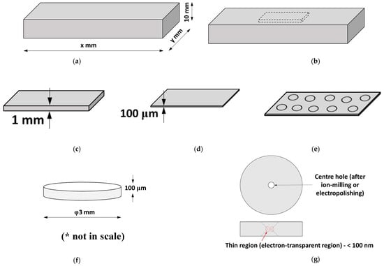
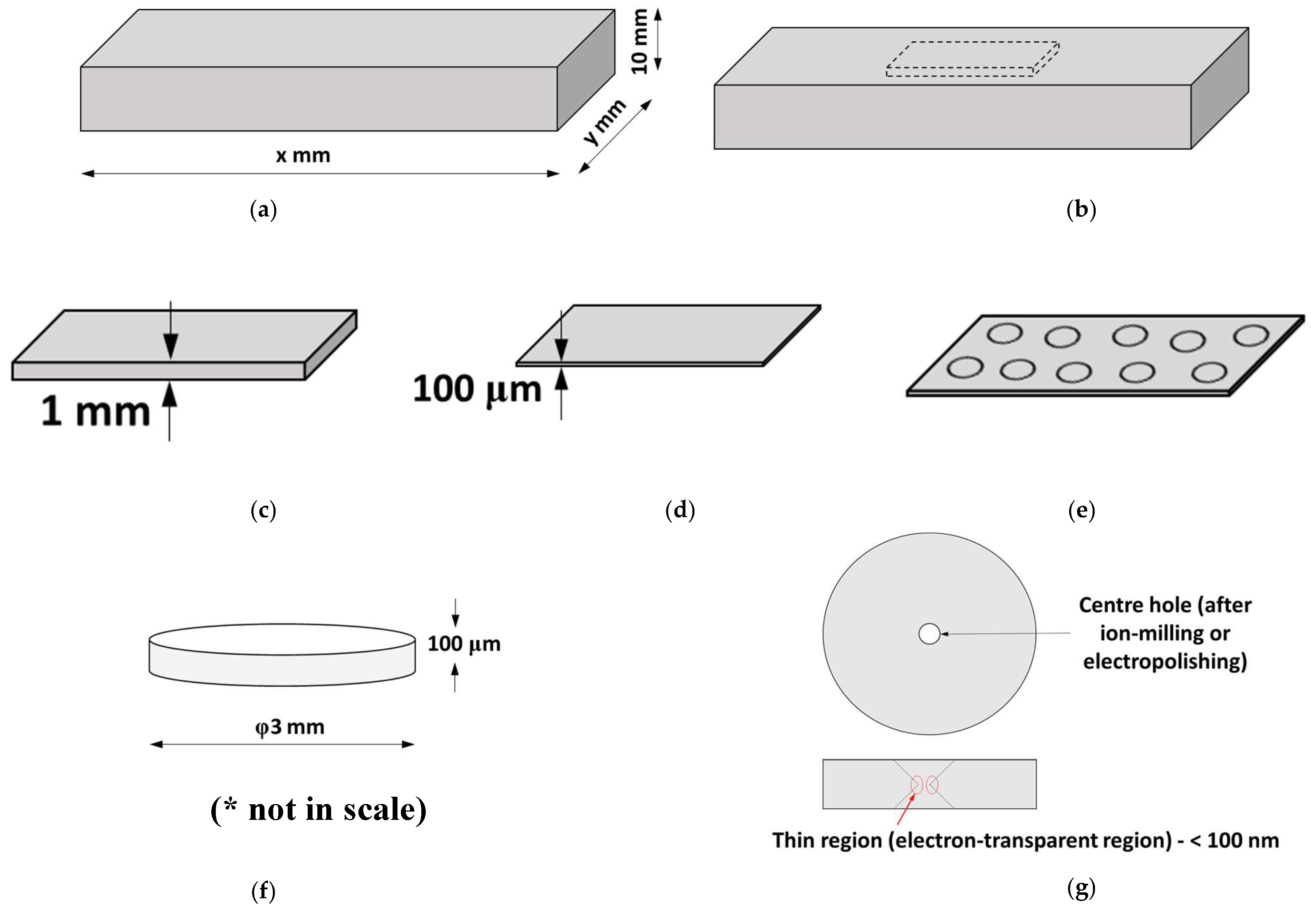
The process of TEM sample preparation involves several key steps to ensure the material is thinned down to an electron-transparent region suitable for high-resolution imaging. First, the material to be characterized is selected (Figure 1a), and the specific region of interest within the material is identified (Figure 1b). A thin slice of the sample, typically with a thickness of 1 mm or less, is then cut from the bulk material using a precision cutting tool (Figure 1c). Traditionally, mechanical polishing is used to reduce the sample thickness to less than 100 μm (Figure 1d); however, in this study, this step is replaced by electrothinning to minimize deformation during thinning. Once the desired thickness is obtained, 3 mm discs are punched from the sample using a disc-punch device (Figure 1e,f). The final step involves electropolishing or ion milling of the discs to create a hole at the centre, with thin regions around the hole where the thickness is less than 100 nm, making the sample suitable for TEM analysis (Figure 1g). Electropolishing is commonly used for surface finishing; however, in the present work, the same principle is used for thickness reduction during TEM sample preparation.
Figure 1.
Schematic of various steps involved in the TEM sample preparation process (sample dimensions are not to scale): (a) bulk material; (b) region of interest; (c) initial sample preparation; (d) mechanical polishing up to 100 μm; (e) disc punching; (f) 3 mm disc (* indicates the given dimensions are not in scale); (g) electron-transparent region.
Furthermore, when materials undergo deformation processes such as cold-rolling, cold-forming, cold-forging, and severe plastic deformation, they develop microstructural defects, primarily dislocations. Typically, TEM microstructural analysis is conducted on these materials to quantify the dislocation density generated by the deformation process. Under these circumstances, during the preparation of TEM samples from these materials, the mechanical polishing step can introduce additional defects if the polishing rate is slightly higher. Consequently, preparing TEM samples from these deformed materials remains a challenge for researchers. However, the proposed electrothinning process does not involve any deformation during material removal. As a result, it may improve the precision of defect-density measurements in TEM microstructural analysis. Furthermore, this process eliminates the generation of internal stresses, as no deformation occurs during material removal.
2. Electrothinning Process
The proposed technique in this study addresses the step c to step d process, i.e., an alternative to mechanical thinning from 1 mm to less than 100 μm, as shown in Figure 1. Before starting TEM sample preparation, it is essential to ensure that the samples are thoroughly cleaned with acetone. Following this, a thick section, approximately 1 mm in thickness, is extracted from the bulk material using either a wire-cut EDM technique or a low-speed diamond cutter to minimize stress and damage.
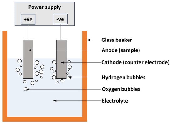
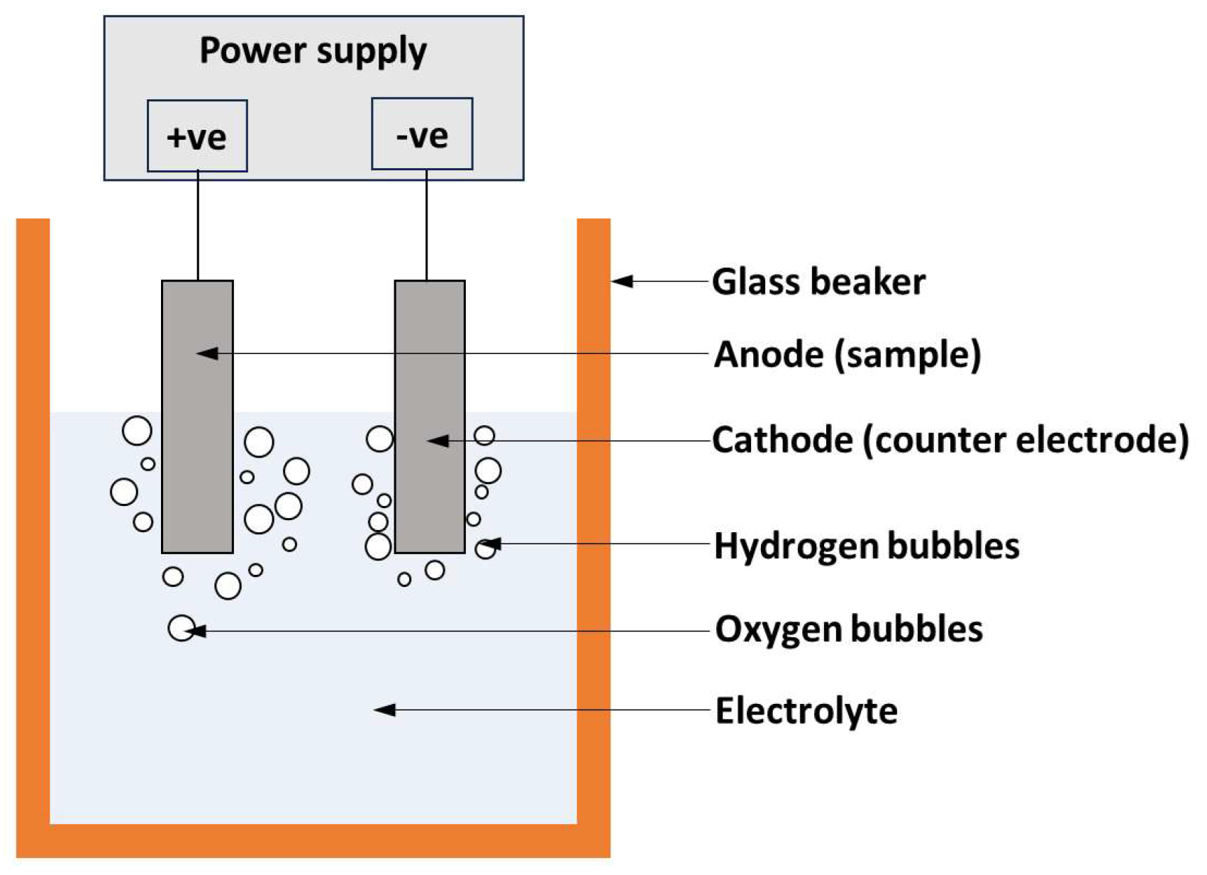
The electrothinning process is an electrochemical method used to remove material layer by layer, allowing precise thinning to the required thickness. In this process, the sample is connected to the positive terminal (anode) of a power supply, while the cathode (counter electrode) is connected to the negative terminal, as illustrated in Figure 2. When an electric current is applied, metal ions are released from the anode and enter the electrolyte solution. The anode (sample) undergoes anodic dissolution, where metal ions are selectively removed from the surface.
Figure 2.
Schematic of the electrothinning process.
In this study, for NiTi alloy, sulfuric acid promotes anodic dissolution by enhancing the electrochemical reaction at the sample surface, while methanol helps in reducing excessive heating and improves dissolution stability during the electrothinning process. The selected electrolyte system helps in obtaining comparatively even thinning across the sample. This results in a highly controlled and uniform material removal process. Several factors, including electrolyte composition, applied voltage, temperature, current density, and processing time, can be adjusted to achieve the desired sample thickness.
As this process is electrochemical in nature, it can also be applied to other conductive metallic materials after optimization of process parameters. This technique can be employed for thinning various pure metals and alloys, given that the processing parameters are optimized. Additionally, electrothinning significantly reduces the need for manual intervention, making it a faster and more efficient alternative compared to conventional mechanical polishing or ion milling techniques.
3. Experimental Methodology for Electrothinning Process
In this study, the electrothinning process was performed on an equiatomic NiTi alloy sheet of thickness 1 mm in annealed condition (sample) as the anode and stainless steel (316L) as the cathode to obtain a sample thickness of less than 100 μm. This was further subjected to electropolishing to get the electron-transparent region in the sample for TEM microstructural imaging. The NiTi sample, initially 1 mm thick, was thinned down to 55 μm (Figure 1b) using an electrolyte solution of H2SO4 (20%) and methanol (80%), at an operating voltage of 10–15V for 20 min. Preliminary trials were carried out at different voltage ranges. At lower voltages (<10V), the material removal rate was very slow and non-uniform thinning was observed. At higher voltages (>15 V), electroxcessive anodic dissolution and localized pitting were noticed. More stable thinning behaviour was observed between 10 and 15 V for the NiTi alloy.
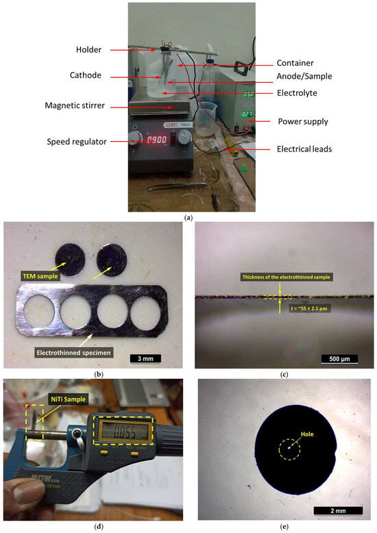
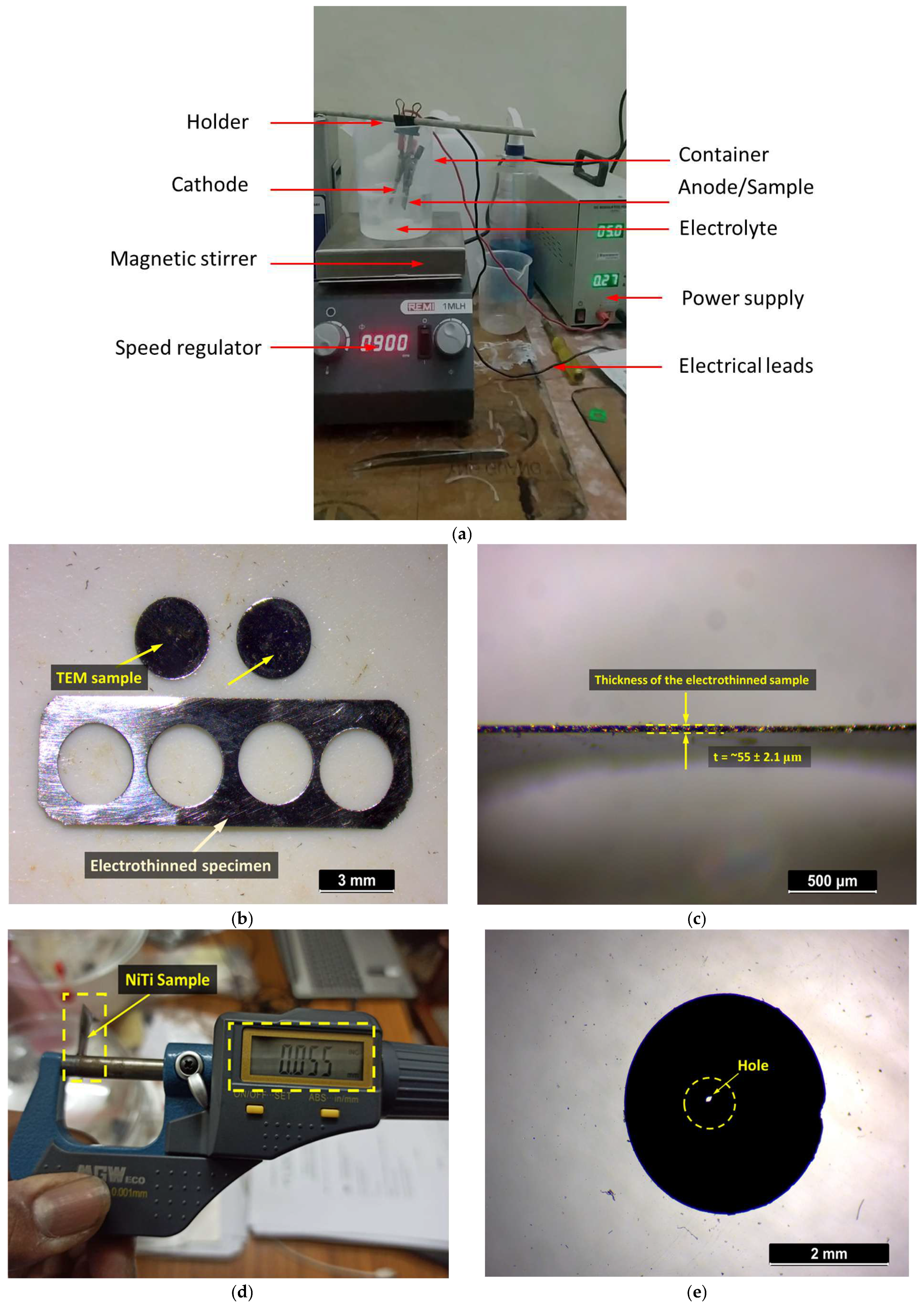
The electrochemical cell setup ensured uniform anodic dissolution, with the NiTi alloy serving as the material to be thinned and the 316L stainless steel acting as the counter electrode, as shown in Figure 3a. A magnetic stirrer (5MLH Model, Remi Elektrotechnik Limited, Mumbai, India) was used to maintain electrolyte homogeneity and prevent the adhesion of the removed material onto the electrodes The experiments were repeated under similar conditions, and comparable thinning behaviour was observed. After the electrothinning process, the samples were cleaned with acetone, then punched into 3 mm discs for TEM imaging, as shown in Figure 3b. The final thinning step was carried out by twin-jet electropolishing using an electrolyte consisting of 15% H2SO4 and 85% methanol at an applied voltage of 12.5 V and a temperature of −30 °C. Electropolishing was continued until a hole formed nearer to the centre, and the region near the hole became electron-transparent, which is suitable for TEM observation. TEM analysis was conducted using a Tecnai 20 model (Thermo Fisher Scientific, Eindhoven, The Netherlands) transmission electron microscope, equipped with selected-area electron diffraction for crystallographic analysis.
Figure 3.
(a) Lab-scale electrothinning setup, (b) TEM specimens punched from the electro-thinned sample, (c) side view showing the thickness of the electro-thinned sample, (d) electro-thinned NiTi sample with a final thickness of 55 μm and (e) NiTi sample after twin-jet electropolishing suitable for TEM observation.
4. Results and Discussions
Effectiveness of Electrothinning in Sample Preparation
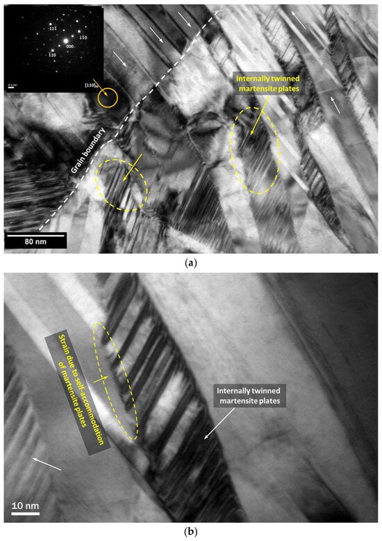
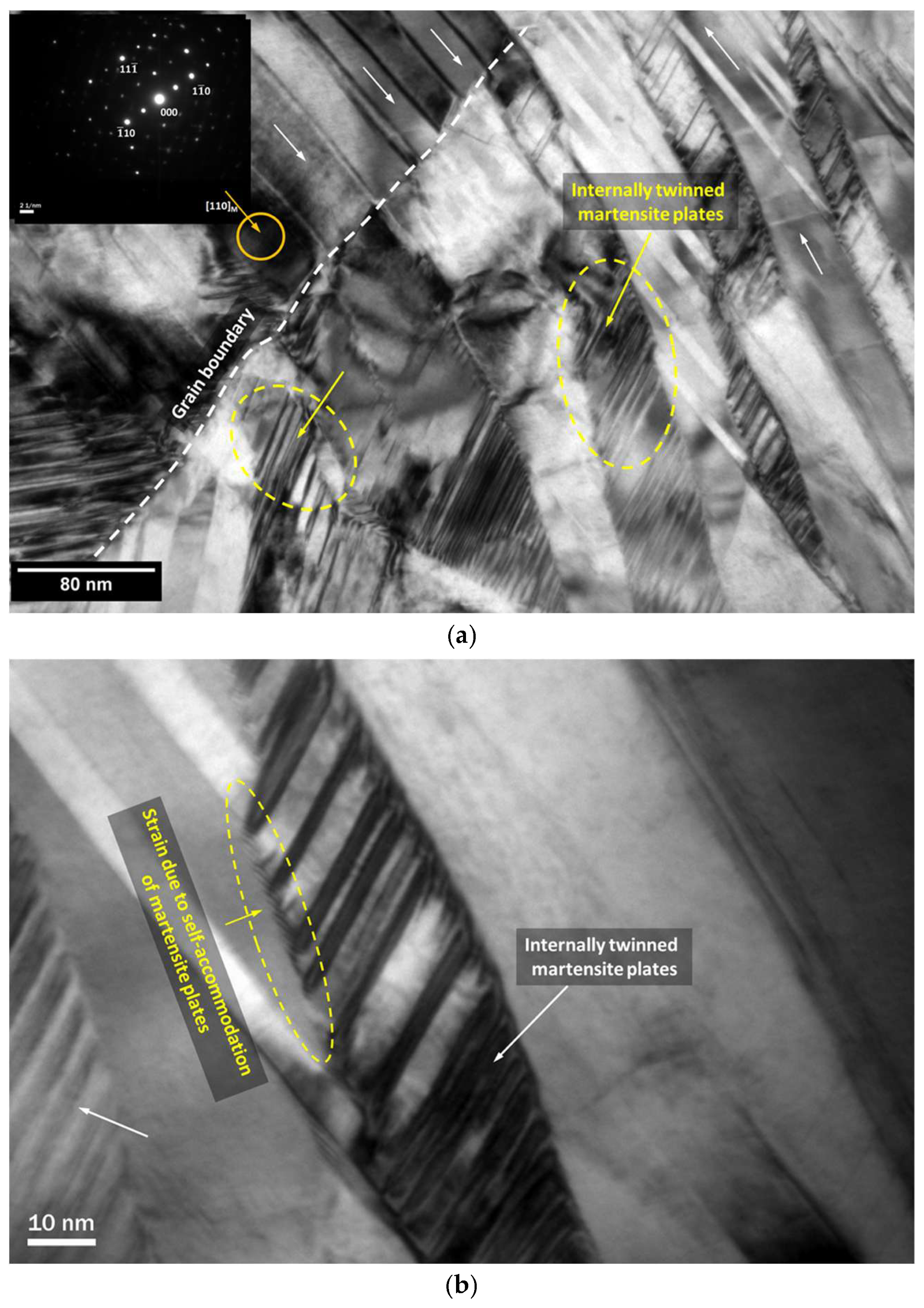
The electrothinning process successfully reduced the thickness of the NiTi alloy sample from 1 mm to 55 μm without causing mechanical stress or defects in about 20 min. The thickness measurements taken at different locations showed comparatively uniform thinning within the standard deviation of about 2.1 μm, as shown in Figure 3c,d. During electrothinning, hydrogen and oxygen bubble formation may affect local current density and material removal uniformity. Continuous stirring by magnetic stirrer was used to minimize bubble adhesion on the sample surface. Unlike conventional mechanical polishing, which uses abrasive forces that can create dislocations or harden the material, electrothinning provides a smooth and stress-free thinning method. TEM images of the electrothinned sample, shown in Figure 4, confirm that there are no signs of deformation or damage, proving that this method is effective for preparing high-quality samples for microstructural analysis. Unlike mechanical polishing, the proposed process did not introduce noticeable deformation during thinning. TEM analysis shows that the electrothinned sample maintains its original microstructure, with no dislocation networks or plastic deformation. Since no mechanical defects are introduced, the sample remains unchanged from its original form, making it suitable for accurate crystallographic and microstructural studies.
Figure 4.
TEM images of the NiTi alloy prepared through electrothinning process (The arrow marks indicate different features of NiTi alloy).
The controlled electrochemical dissolution mechanism of electrothinning yields uniform thinning across the sample. According to literature reports, ion milling and FIB-based preparation may introduce preferential thinning and ion-induced defects [20,21], whereas electrothinning provides a homogeneous material removal rate. During electrothinning, passivation and oxide layer formation can influence the uniformity of material removal. In NiTi alloys, the formation of a stable oxide layer on the surface may reduce the dissolution rate and affect thinning uniformity. The acidic electrolyte environment provided by H2SO4 assists in minimizing excessive oxide build-up and promotes continuous anodic dissolution. In addition, methanol helps in maintaining process stability and reducing localized heating during electrothinning. Under the selected operating conditions (10–15 V), stable material removal was achieved without significant passivation during the thinning process.
The application of optimized voltage (10–15V) and electrolyte composition (H2SO4 and methanol) for NiTi alloy ensured smooth, layer-by-layer thinning, preventing local variations in thickness that could impact TEM imaging. TEM observations did not show noticeable preparation-induced defects in the electrothinned samples. This indicates that the electrothinning process provides stress-free material removal suitable for accurate microstructural characterization. The comparison of the proposed technique with the other methods are shown in Table 1.
Table 1.
Comparative analysis of electrothinning process with other methods.
5. Challenges in the Electrothinning Process
Although electrothinning offers a promising alternative for TEM sample preparation, some challenges must be addressed for its effective implementation. One of the primary challenges is the optimization of process parameters, including voltage, electrolyte composition, temperature, and processing time. Improper parameter selection can lead to uneven thinning, pitting, or excessive material removal, affecting sample quality. Additionally, different materials exhibit unique electrochemical behaviour, making it necessary to customize electrolyte formulations and process conditions for each material to ensure uniform thinning. At lower voltages (<10 V), insufficient anodic dissolution resulted in incomplete and non-uniform thinning. In contrast, voltages above 15 V caused localized heating, unstable dissolution behaviour, surface irregularities, and excessive edge thinning.
The choice and handling of electrolytes also present challenges, as many contain strong acids that pose safety hazards due to their corrosive and toxic nature. Proper handling, storage, and disposal of these chemicals must be considered to minimize environmental impact. Furthermore, while electrothinning generally provides a smooth surface finish, minor irregularities or thickness variations can still occur, necessitating additional electropolishing to achieve a fully electron-transparent region suitable for TEM imaging. Another limitation of electrothinning is its applicability mainly to conductive materials, restricting its use for non-metallic samples, such as ceramics and polymers. For such materials, alternative methods like ion milling may still be necessary. Additionally, achieving precise control over the final sample thickness is critical, as over-thinning can result in sample rupture, while under-thinning may require further processing.
The requirement for a controlled experimental setup, including a stable power supply, optimized electrodes, and electrolyte circulation, adds another layer of complexity. Any inconsistencies in these factors can affect reproducibility and overall reliability. Despite these challenges, electrothinning remains a highly valuable technique for TEM sample preparation, particularly for researchers who require a stress-free thinning method without mechanically induced defects. Although the present work is limited to NiTi shape memory alloy, the proposed electrothinning methodology can be extended to other metallic materials through appropriate optimization of electrolyte composition and operating parameters.
6. Conclusions
The present study showed the feasibility of using the electrothinning process as an alternative technique for intermediate TEM sample preparation. The proposed process reduced the thickness of the NiTi alloy sample from 1 mm to 55 μm through controlled anodic dissolution using an H2SO4–methanol electrolyte system. The operating voltage range of 10–15 V resulted in stable and comparatively uniform thinning behaviour without excessive pitting or localized damage. The electrothinning process avoided mechanically induced stress and deformation that are commonly associated with conventional grinding and polishing techniques. TEM analysis confirmed that the electrothinned samples retained the original microstructure without noticeable preparation-induced defects or deformation features. The process also reduced manual effort and sample preparation time when compared to conventional mechanical thinning methods. The results of the present work indicate that electrothinning can be used for conductive metallic materials after selecting appropriate electrolyte and operating conditions. The present approach can reduce manual effort and preparation time during TEM sample preparation suitable for accurate microstructural characterization. Further studies can be carried out to optimize the process for different metallic alloys and to improve thickness control and process repeatability.
Author Contributions
Conceptualization, S.G. and B.P.; Methodology, S.G.; Writing—Original Draft, B.P., Investigation, S.G. and B.P.; Formal analysis, S.K., B.L., M.A. and S.K.S., Writing—review and editing, S.K., B.L., S.K.S. and M.A. All authors have read and agreed to the published version of the manuscript.
Funding
This research received no external funding.
Data Availability Statement
All data necessary to reproduce the results presented in this study are included within the manuscript. No additional datasets were generated or analyzed during the current study.
Conflicts of Interest
The authors confirm that there are no conflicts of interest associated with this publication and that there has been no significant financial support that could have influenced the outcome of this research.
References
- Zuo, J.M.; Spence, J.C.H. Advanced Transmission Electron Microscopy, 1st ed.; Springer: New York, NY, USA, 2017. [Google Scholar]
- Inkson, B.J. Scanning electron microscopy (SEM) and transmission electron microscopy (TEM) for materials characterization. In Materials Characterization Using Nondestructive Evaluation (NDE) Methods; Elsevier: Amsterdam, The Netherlands, 2016; pp. 17–43. [Google Scholar]
- Nowakowski, P.; Bonifacio, C.; Ray, M.; Fischione, P. Combining emerging sample preparation methods, SEM, and TEM investigations for microelectronics device characterization at multiple scales. Microsc. Microanal. 2019, 25, 688–689. [Google Scholar] [CrossRef] [Scilit]
- Singh, R. Fundamentals of TEM Sample Preparation. In Transmission Electron Microscopy Sample Preparation: From Specimen to Micrograph; Springer: Berlin/Heidelberg, Germany, 2025; pp. 21–42. [Google Scholar]
- Ayache, J.; Beaunier, L.; Boumendil, J.; Ehret, G.; Laub, D. Sample Preparation Handbook for Transmission Electron Microscopy: Techniques; Springer Science Business Media: Berlin/Heidelberg, Germany, 2010; Volume 2. [Google Scholar]
- Rajput, N.S.; Sloyan, K.; Anjum, D.H.; Chiesa, M.; Al Ghaferi, A. A user-friendly FIB lift-out technique to prepare plan-view TEM sample of 2D thin film materials. Ultramicroscopy 2022, 235, 113496. [Google Scholar] [CrossRef] [Scilit] [PubMed]
- Sezen, M.; Janecek, M. Focused Ion Beams (FIB)—Novel methodologies and recent applications for multidisciplinary sciences. In Modern Electron Microscopy in Physical and Life Sciences; InTech: London, UK, 2016; pp. 121–140. [Google Scholar]
- Li, J.; Malis, T.; Dionne, S. Recent advances in FIB-TEM specimen preparation techniques. Mater. Charact. 2006, 57, 64–70. [Google Scholar] [CrossRef] [Scilit]
- Minenkov, A.; Šantić, N.; Truglas, T.; Aberl, J.; Vukušić, L.; Brehm, M.; Groiss, H. Advanced preparation of plan-view specimens on a MEMS chip for in situ TEM heating experiments. MRS Bull. 2022, 47, 359–370. [Google Scholar] [CrossRef] [Scilit] [PubMed]
- Delobbe, A.; Salord, O.; Hrncir, T.; David, A.; Sudraud, P.; Lopour, F. High speed TEM sample preparation by Xe FIB. Microsc. Microanal. 2014, 20, 298–299. [Google Scholar] [CrossRef] [Scilit]
- Zhong, X.; Wade, C.A.; Withers, P.J.; Zhou, X.; Cai, C.; Haigh, S.J.; Burke, M.G. Comparing Xe+ pFIB and Ga+ FIB for TEM sample preparation of Al alloys: Minimising FIB-induced artefacts. J. Microsc. 2021, 282, 101–112. [Google Scholar] [CrossRef] [Scilit] [PubMed]
- Bassim, N.D.; De Gregorio, B.T.; Kilcoyne, A.L.D.; Scott, K.; Chou, T.; Wirick, S.; Cody, G.; Stroud, R.M. Minimizing damage during FIB sample preparation of soft materials. J. Microsc. 2012, 245, 288–301. [Google Scholar] [CrossRef] [Scilit]
- Liu, J.; Niu, R.; Gu, J.; Cabral, M.; Song, M.; Liao, X. Effect of ion irradiation introduced by focused ion-beam milling on the mechanical behaviour of sub-micron-sized samples. Sci. Rep. 2020, 10, 10324. [Google Scholar] [CrossRef] [Scilit] [PubMed]
- Baxter, F.; Garner, A.; Topping, M.; Hulme, H.; Preuss, M.; Frankel, P. Phase stability of zirconium oxide films during focused ion beam milling. J. Nucl. Mater. 2018, 504, 176–180. [Google Scholar] [CrossRef] [Scilit]
- Rao, D.V.S.; Muraleedharan, K.; Humphreys, C.J. TEM specimen preparation techniques. Microsc. Sci. Technol. Appl. Educ. 2010, 2, 1232. [Google Scholar]
- Franken, L.E.; Boekema, E.J.; Stuart, M.C.A. Transmission electron microscopy as a tool for the characterization of soft materials: Application and interpretation. Adv. Sci. 2017, 4, 1600476. [Google Scholar] [CrossRef] [Scilit] [PubMed]
- Singh, R. Sample Preparation for Quantitative Analysis Under TEM. In Transmission Electron Microscopy Sample Preparation: From Specimen to Micrograph; Springer: Berlin/Heidelberg, Germany, 2025; pp. 187–223. [Google Scholar]
- Yang, G.; Wang, B.; Tawfiq, K.; Wei, H.; Zhou, S.; Chen, G. Electropolishing of surfaces: Theory and applications. Surf. Eng. 2017, 33, 149–166. [Google Scholar] [CrossRef] [Scilit]
- Han, W.; Fang, F. Fundamental aspects and recent developments in electropolishing. Int. J. Mach. Tools Manuf. 2019, 139, 1–23. [Google Scholar] [CrossRef] [Scilit]
- Uzuhashi, J.; Ohkubo, T. Systematic study of FIB-induced damage for the high-quality TEM sample preparation. Ultramicroscopy 2024, 262, 113980. [Google Scholar] [CrossRef] [Scilit] [PubMed]
- Zhong, X.; Zhou, X.; Haigh, S.J.; Withers, P.J.; Burke, M.G. Challenges in FIB TEM sample preparation: Damage issues and solutions. Microsc. Microanal. 2022, 28, 60–62. [Google Scholar] [CrossRef] [Scilit]

Disclaimer/Publisher’s Note: The statements, opinions and data contained in all publications are solely those of the individual author(s) and contributor(s) and not of MDPI and/or the editor(s). MDPI and/or the editor(s) disclaim responsibility for any injury to people or property resulting from any ideas, methods, instructions or products referred to in the content. |
© 2026 by the authors. Licensee MDPI, Basel, Switzerland. This article is an open access article distributed under the terms and conditions of the Creative Commons Attribution (CC BY) license.