


Abstract
This study investigates the effects of deposition angle and arc current on the surface morphology and optical response of Ti coatings obtained by unfiltered cathodic arc evaporation for spectrally selective solar-thermal applications. 100 nm-thick Ti films were deposited at normal (0°) and oblique (80°) angles of incidence, with arc currents of 65 A and 90 A, respectively. The SEM measurements revealed the characteristic arc-generated microdroplet population. At normal incidence (0°), droplets are predominantly spherical and relatively uniformly distributed, whereas at 80° incidence, many droplets exhibit elongated footprints aligned with the incoming flux from the Ti cathode. This behavior is consistent with oblique-angle deposition (OAD), where the arrival geometry can promote self-shadowing and transient droplet spreading before solidification. AFM confirms an increase in nanoscale roughness, whereas GIXRD indicates nanocrystalline α-Ti and cubic TiO, with maximum crystallinity for 0°/65 A. Contact-angle measurements demonstrate a transition from hydrophobic 316L (~103°) to moderately hydrophilic Ti-coated surfaces (~68–72°), with only minor dependence on deposition geometry. Optical reflectance in the 400–800 nm range is significantly lower for Ti-coated glass and is further reduced for OAD films, indicating enhanced solar absorptance.
1. Introduction
Solar thermal collectors are among the most efficient ways to convert solar radiation into thermal energy. In principle, a solar thermal collector concentrates sunlight on an absorbing surface, converts it into heat, and transfers it to a heat-transfer fluid, which is then used to produce domestic hot water for space heating, or for industrial processes at low-to-medium temperatures [1]. There are several types of solar thermal collectors, such as glazed flat-plate collectors, evacuated tube collectors, and parabolic or Fresnel concentrating collectors, etc., which can reach higher temperatures for industrial applications [2]. All these technologies aim to maximize the amount of solar energy captured and to reduce heat losses to the environment by using optimized combinations of absorber materials, cover glazing, thermal insulation, and complex geometric configurations [3,4]. In this context, the design and fabrication of spectrally selective coatings are currently among the most active research directions for performance optimization. In general, the spectral selectivity of such coatings for solar collectors can be achieved through different optical structures [2], as follows: intrinsic/textured/photonic absorber coatings [5,6,7], semiconductor-metal tandem structures [8], ceramic metal (cermet) type structures [9] or transition-metal oxides with spinel-type structures [10]. Spectral tailoring at the boundary between the visible and infrared spectral ranges can be achieved through structural or architectural design methods, such as multilayers, cermets, and oblique-angle-deposited nanostructures [11,12,13]. These approaches modify the effective optical constants and the interaction between light and matter. Additionally, spectral tailoring can be achieved through compositional tuning, including alloying and chemical doping (both cationic and anionic) [14,15,16]. This is especially relevant in semiconductors, where adjustments to the electronic structure can be directly made [11,12]. In this context, oblique angle deposition (OAD) is of interest because it allows the engineering of nanostructured coatings for energy-harvesting and optoelectronic applications, owing to its ability to generate highly porous, columnar architectures whose morphology is strongly dependent on the deposition angle and process conditions [17].
Among materials relevant to solar-thermal coatings, titanium is a promising candidate for oblique-angle nano-structuring due to its tunable optical response, surface plasmon behavior, and thermal stability. In textured forms, Ti can exhibit reduced visible reflectance and enhanced solar absorptance, making it suitable not only as an intrinsic absorber but also as a base layer within multilayer structures. Moreover, titanium and its compounds are already used in high-temperature solar-selective coatings due to their tunable optical constants, high melting point, and chemical stability [18,19]. According to Ref. [20], for Ti thin films deposited by electron-beam evaporation at a high incidence angle of 84° and varying substrate temperatures, the observed morphology changes are consistent with a competition between shadowing length and adatom diffusion length, with porous, inclined microcolumns forming in all cases where shadowing dominates over surface diffusion. Dervaux et al. reported on Ti thin films grown by glancing-angle magnetron sputtering (MS-GLAD) [21], in which the combined use of experiments and kinetic Monte Carlo simulations showed that increasing the deposition angle results in highly porous films. These films are made of well-separated tilted columns, whose tilt angle β is systematically lower than the geometrical angle α due to parallel-momentum conservation and anisotropic adatom diffusion along the vapor beam [21]. In the study of M. Bordbari et al. on Ba0.5Sr0.5TiO3 thin films grown by oblique angle deposition [22], it was shown that large incident angles (≈70–75°) strongly enhance nanocolumnar growth, increase surface roughness, and lead to marked changes in optical constants (higher refractive index and reduced band gap) compared with normal incidence. At 75°, the films exhibited well-aligned nanostructures and a clear modification of texture, indicating that the incident angle can be used as an efficient control parameter for both morphology and optics [22]. In the case of thermal evaporation, the kinetic energy of the vapor species arriving at the surface is very low (~0.2 eV), so growth is practically influenced by geometric shadowing and competitive growth effects, with no significant kinetic-energy-driven processes at the substrate [23]. Most studies on oblique angle deposition (OAD) have been carried out using low-energy vapor fluxes generated by thermal evaporation, magnetron sputtering or ion-beam sputtering [23,24], where nanocolumnar growth is influenced by geometric shadowing and limited adatom mobility. On the other hand, cathodic arc evaporation produces a highly ionized metal plasma in which Ti ions exhibit much higher kinetic energies, with energy distributions extending up to 200 eV and average energies situated in the tens-of-eV range, depending on pressure and cathode composition [25]. This energetic regime is expected to modify the evaporation-based OAD by coupling the incidence angle to both shadowing-driven nanocolumnar growth and ion-bombardment-driven microstructural changes. Despite the extensive use of Ti-based coatings deposited by cathodic arc in hard-coating and tooling applications [26,27], few studies of Ti thin films grown by oblique-angle cathodic arc deposition and their potential as solar-thermal absorbers have been reported [28,29]. In this work, we address this gap by investigating Ti thin films deposited by unfiltered cathodic arc at normal (0°) and oblique (80°) incidence for two arc currents (65 A and 90 A), on Si(100), 316L stainless steel, and microscope glass substrates. For a thickness of ~100 nm, we correlate the incidence angle and arc current with film thickness uniformity, surface morphology (SEM, AFM), composition (EDS), structure (GIXRD), wetting behavior (distilled water contact angle), and UV–Vis reflectance.
2. Materials and Methods
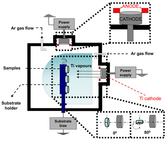
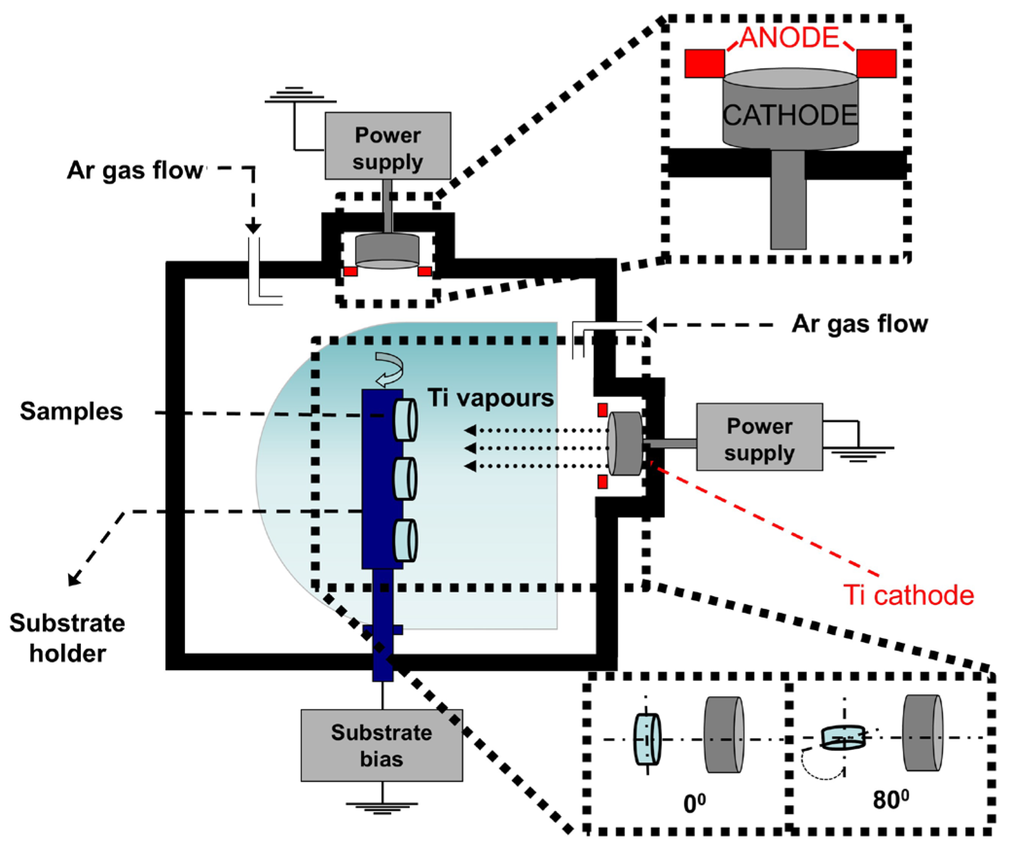
Titanium thin films were deposited by unfiltered cathodic arc evaporation using a Ti cathode (Kurt Lesker, Jefferson Hills, PA, USA, 99.99% purity). The films were grown on three types of substrates: mechanically polished 316L stainless steel discs (Ø25 mm, thickness ≈ 0.5 mm), Si(100) wafers of 10 × 10 mm pieces (thickness ≈ 0.5 mm) and microscope glass slides (10 × 15 mm, thickness ≈ 1 mm). Two arc-discharge current values, 65 A and 90 A, were used to evaluate the effects of plasma energy and ion flux on film growth. The base pressure in the deposition chamber was ~10−3 Pa, while the working pressure during deposition was 10−3 Pa. The target-to-substrate distance was kept at ~30 cm, and no external substrate heating was applied. Before deposition, the substrate holder was biased at −850 V, and substrates were sputter-etched in an Ar+ plasma for 3 min. For each current, coatings were deposited in two geometries: at normal incidence (0°) and at an oblique incidence angle of 80°, by tilting the substrate holder with respect to the cathode–substrate axis (Figure 1). A substrate bias of −15 V was applied during deposition. The deposition times were adjusted to obtain continuous Ti layers with a thickness of approximately 100 nm, namely 53 s (316L/Ti 0°, 65 A), 13 s (316L/Ti 0°, 90 A), 56 s (316L/Ti 80°, 65 A) and 87 s (316L/Ti 80°, 90 A) under otherwise identical process conditions. A Jasco V-670 spectrophotometer (Jasco, Tokyo, Japan) was used to characterize the optical properties of the Ti thin films in the UV–visible–near-IR range. Reflectance spectra were measured with an ARSN-733 accessory, which combines a single concave mirror with a 60 mm-diameter integrating sphere; according to the manufacturer, the relative error in absolute reflectance measurements is 1.5% at an incidence angle of 5°. Spectra were recorded between 200 and 800 nm with a scan speed of 400 nm/min. Surface topography was investigated by atomic force microscopy (AFM, Veeco–Bruker, Billerica, MA, USA) in intermittent-contact mode on 5 µm × 5 µm areas, with a scan rate of 0.3 Hz and an in-plane resolution of 1.95 nm/pixel (512 × 512 pixels). The AFM measurements were performed using an RTESPA probe (tip radius ~8 nm, resonance frequency ~300 kHz, spring constant 40 N/m). The film morphology and elemental composition were further examined by scanning electron microscopy (SEM, Hitachi TM3030Plus, Tokyo, Japan) equipped with an energy-dispersive X-ray spectroscopy (EDS) system (Quantax 70, Bruker, Billerica, MA, USA). The static water contact angle (CA) was measured by the sessile drop method using a KSV-Instruments Attention TL101 goniometer (Biolin Scientific, Stockholm, Sweden). All measurements were performed at room conditions (22 ± 0.5 °C, 40% relative humidity) with distilled water as the probe liquid. A 5 μL droplet was dispensed onto the sample surface using a Hamilton micro-syringe, and a TL101 integrated CCD camera recorded its profile. For each sample, three measurements were taken and the results are expressed as average values ± standard deviation (SD).
Figure 1.
Schematic representation of the cathodic arc deposition setup at normal incidence (0°) and oblique incidence (80°).
The crystalline structure was investigated using a SmartLab diffractometer (Rigaku, Tokyo, Japan) equipped with a five-axis vertical goniometer, a high-resolution incident-beam optical system, and a 9 kW Cu rotating anode (λ = 1.540597 Å). The thin films were analyzed in parallel-beam geometry, and data were collected over a 2θ range of 30–100°, with an incidence angle of 1° and a scanning speed of 3°/min. The thickness of the films was determined by surface profilometry, measuring the step height between the substrate and the film surface. For this purpose, a Dektak 150 profilometer from Veeco (Veeco Instruments, Plainview, NY, USA) equipped with a 2.5 µm stylus tip was used. To meet the requirements of each characterization technique, Ti films were deposited in the same run on three substrates mounted on the same holder: 316L stainless steel discs, Si(100) wafers, and microscope glass slides. Unless otherwise stated, SEM/EDS/wettability results refer to coatings deposited on 316L substrates; AFM/GIXRD/thickness results refer to coatings obtained on Si(100); and optical reflectance spectra refer to coatings on microscope glass slides.
3. Results
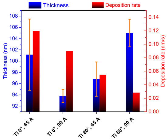
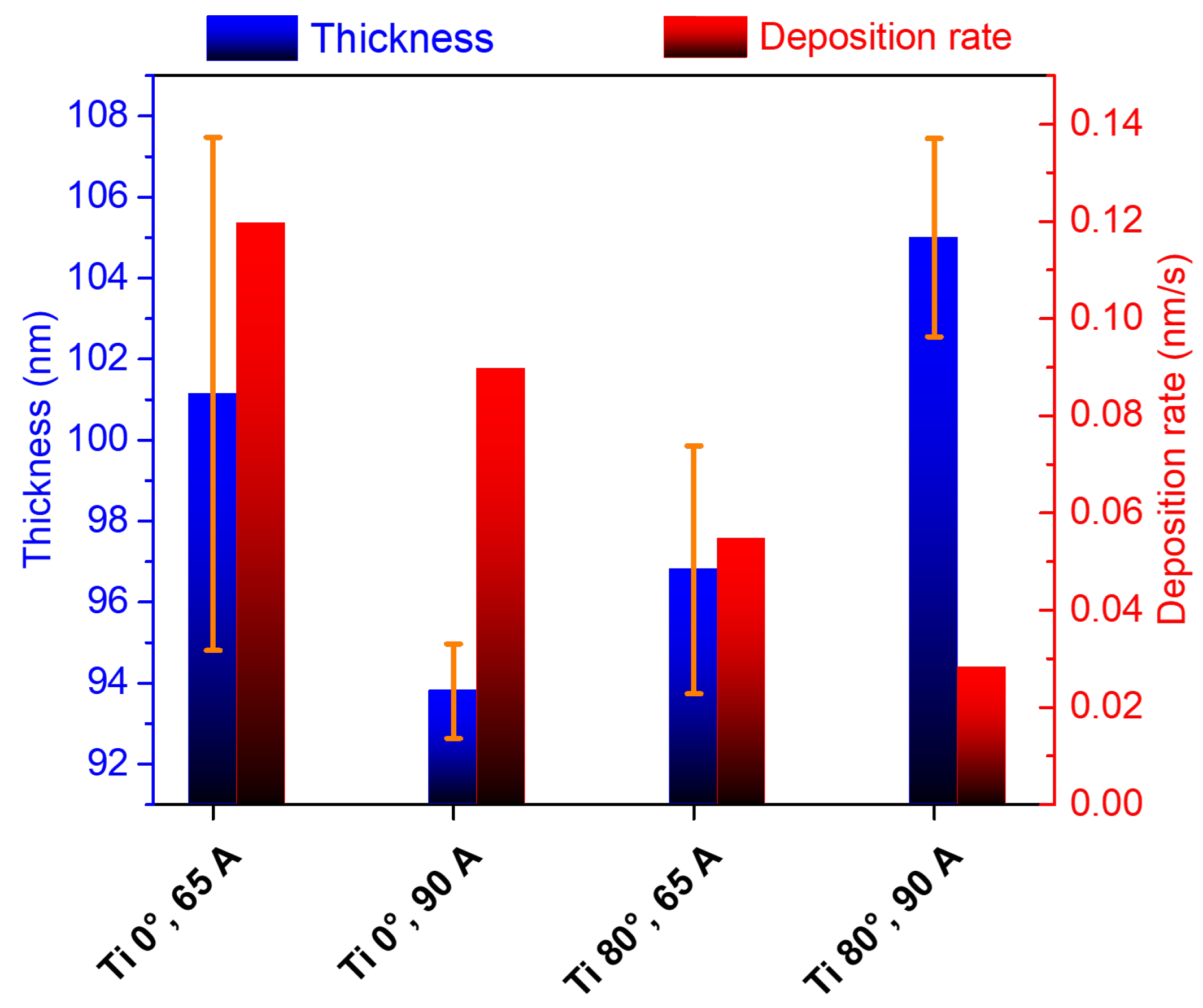
For the Ti layers, the deposition time was adjusted to ensure all coatings reached approximately 100 nm in thickness, regardless of arc current or incidence angle. As summarized in Figure 2, the measured thickness values range from 94 to 105 nm, with standard deviations of ~1–6 nm, in good agreement with the profilometer’s accuracy (±5%). As shown, the calculated deposition rates depend on both the incidence angle and the arc current. At normal incidence, the rate decreases from ~0.12 nm/s (65 A) to ~0.09 nm/s (90 A), while for oblique deposition at 80° it drops further to ~0.055 nm/s (65 A) and ~0.028 nm/s (90 A), i.e., to less than one third of the normal-incidence rate at 90 A. This monotonic decrease in deposition rate with increasing incidence angle is consistent with oblique-angle deposition, where geometric shadowing and a reduced projected collection area lower the effective flux at the substrate. Similar trends have been reported for highly ionized PVD plasmas, in particular in high power impulse magnetron sputtering (HiPIMS), where an increased peak discharge current and ionization degree lead to a loss in deposition rate due to self-sputtering and back-attraction of metal ions to the target [30].
Figure 2.
Film thickness (blue) and deposition rate (red) of Ti thin films deposited by cathodic arc at normal (0°) on Si100 substrates and oblique (80°) incidence for arc currents of 65 A and 90 A.
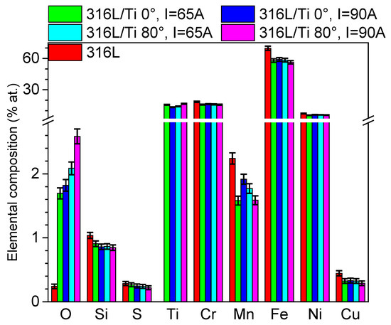
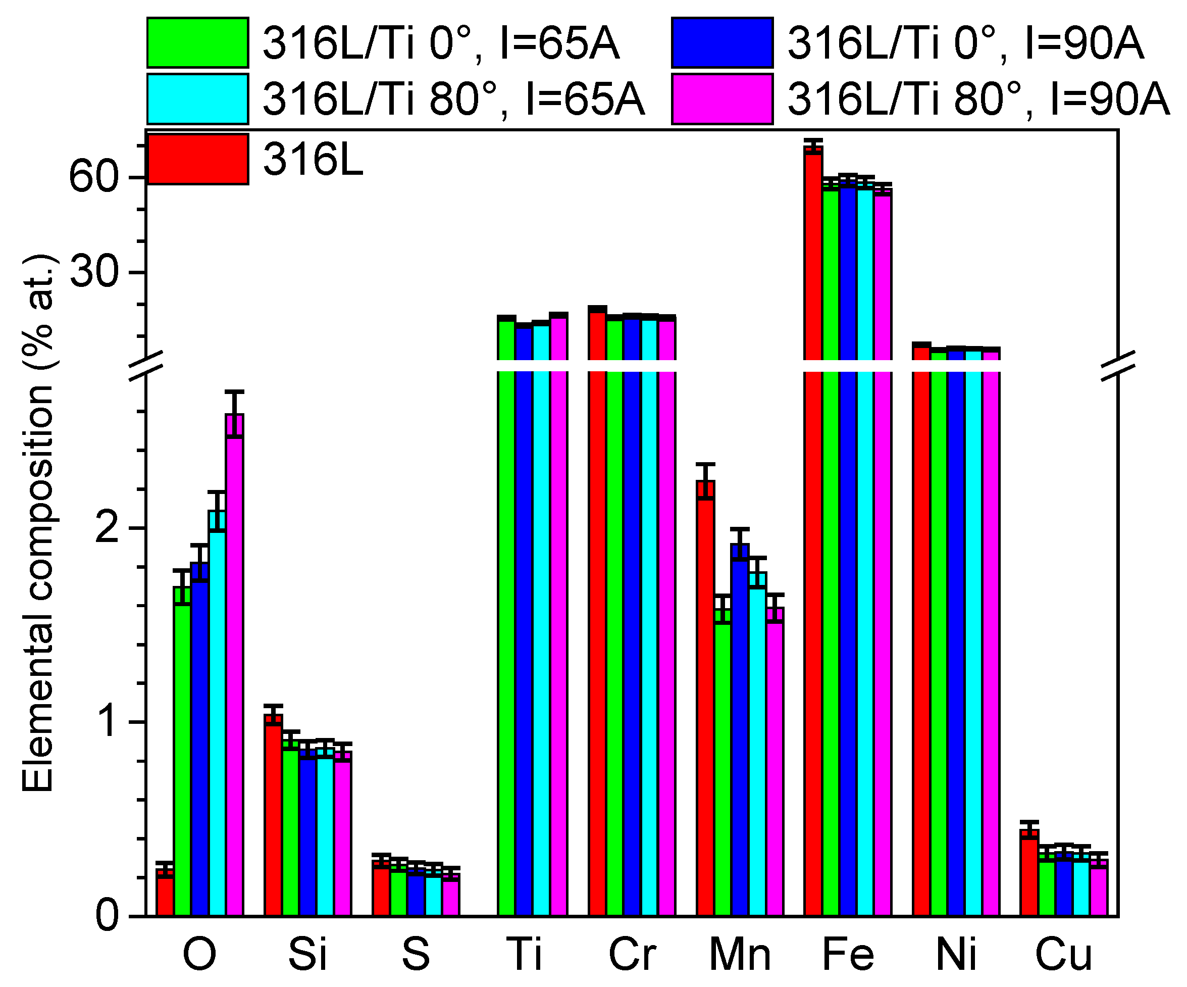
The EDS compositional analysis (Figure 3) shows that all single Ti layers deposited on 316L contain, in addition to titanium, a measurable fraction of oxygen. However, the O content is systematically higher for the samples deposited at 90 A—both at 0° and 80°—compared with those deposited at 65 A. At 90 °A, the density and size of the microdroplets increase slightly, and the surface roughness becomes more pronounced, thereby increasing the specific area exposed to air oxidation and facilitating oxygen diffusion along the droplet boundaries and the underlying Ti layer. For the bare 316L substrate, the EDS results confirm the typical stainless-steel composition: Fe ~70 at.%, Cr ~18–19 at.%, Ni ~7 at.%. After Ti deposition at normal incidence (0°), a significant Ti fraction appears in the EDS spectrum (~13–16 at.%), while Fe decreases to ~56 at.%, Cr to ~16–17 at.%, and Ni to ~6 at.%. In parallel, the oxygen content increases by nearly an order of magnitude, from ~0.2 at.% to ~1.7–2.5 at.%, indicating partial oxidation of the Ti film. For all samples, Ti remains a secondary element, with values of 13–17 at.%, varying slightly with the physical thickness (Figure 2). The relatively high Fe, Cr, and Ni contents reflect the fact that the EDS penetration depth exceeds the ~100 nm film thickness, thus producing a significant contribution from the 316L substrate.
Figure 3.
Atomic concentrations corresponding to Ti layers deposited on 316L substrates at 0° and 80°, with ITi = 65 A and 90 A.
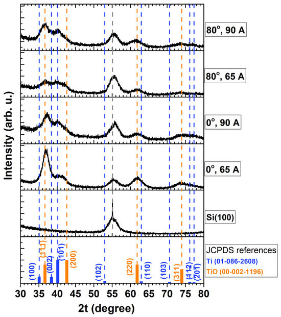
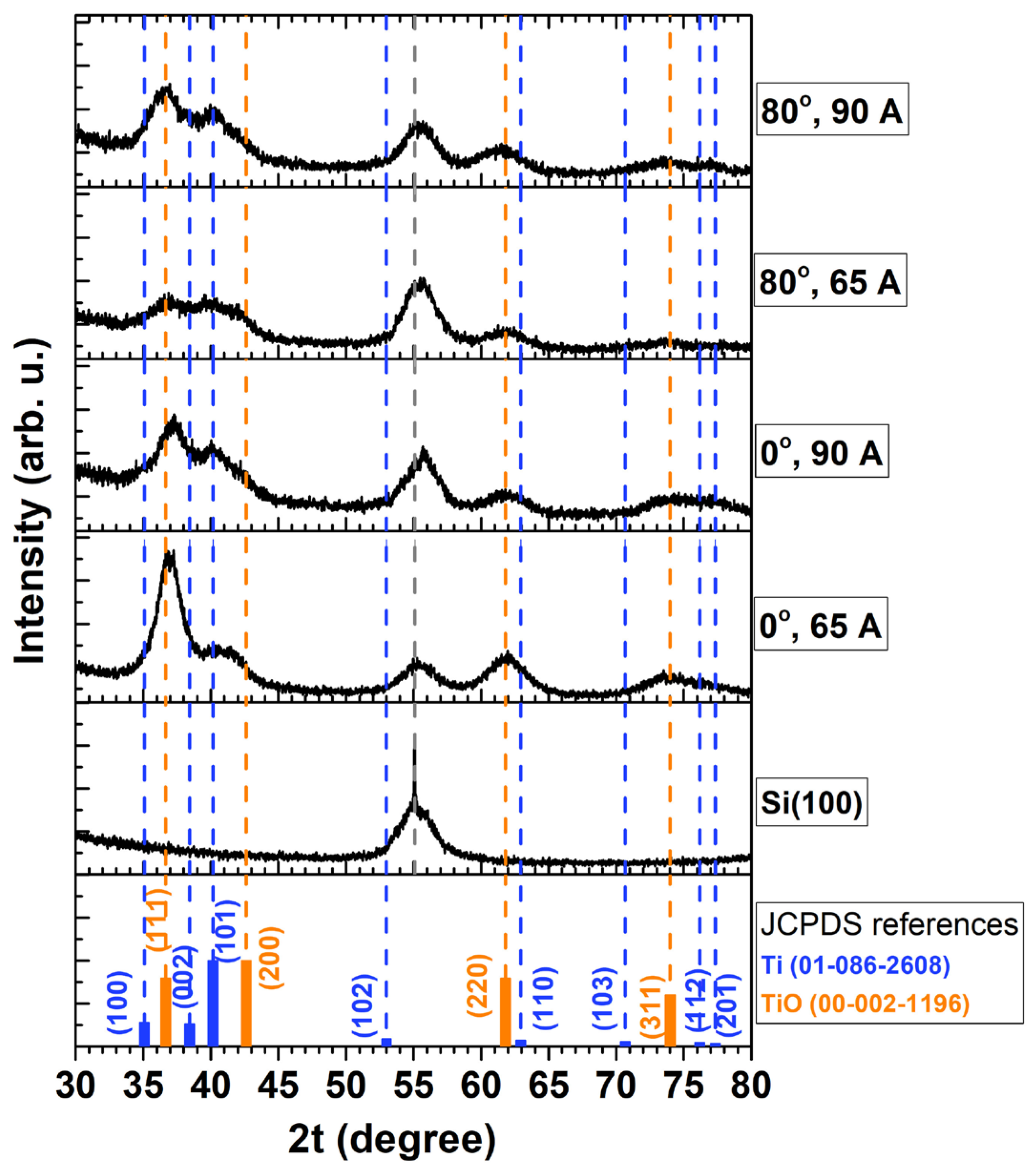
The GIXRD patterns shown in Figure 4 correspond to Ti thin films deposited on Si(100) substrates at incident angles of 0° and 80°, using cathode currents of 65 A and 90 A, respectively. Under all deposition conditions, a weak diffraction peak originating from the Si substrate is observed at about 2θ = 55.0°. Besides this feature, the GIXRD patterns reveal contributions that can be attributed to the hexagonal close-packed (hcp) α-Ti phase and the cubic TiO phase, c-TiO, in agreement with the reference data JCPDS 1-084-3903 and JCPDS 0-002-1196, respectively.
Figure 4.
Grazing-incidence XRD patterns corresponding to Ti/Si(100) thin films and Si(100) substrate.
In the low-angle region (2θ ≈ 34–43°), two main diffraction features are observed, resulting from overlapping reflections of α-Ti and c-TiO phases: α-Ti(100), c-TiO(111), α-Ti(002), α-Ti(101), and c-TiO(200). The peak located at about 2θ = 36.8° is predominantly due to x-ray diffraction from c-TiO(111) planes, while the peak near 2θ = 40.1° mainly arises from α-Ti(101) planes. In the 2θ range 2θ = 60–65°, the observed diffraction feature is associated with the superposition of c-TiO(220) and α-Ti(110) reflections. At higher angles, 2θ = 70–80°, the diffraction pattern exhibits overlapping contributions from α-Ti(103), c-TiO(311), α-Ti(112) and α-Ti(201).
The low intensity and considerable broadening of these reflections indicate that the Ti-based thin films are nanocrystalline, with small crystallite sizes and a high density of structural defects [31].
We note that the 2ϴ/ϴ diffraction patterns, recorded in symmetric geometry, show no distinct diffraction features for all samples, except for the Ti-0°-65A sample, which exhibits a single peak corresponding to c-TiO(111). These results are consistent with the small thickness and the low crystallinity of the films, which hinder the detection of weak diffraction signals in symmetric geometry, but also, it indicates that the films are textured, as suggested by differences in the relative peak intensities compared to the JCPDS reference data (Figure 4).
From Figure 3 data, we concluded that the oxygen content of the films increases systematically with both substrate tilt angle and discharge current, from sample Ti-0°-65A to Ti-80°-90A. Lattice parameter refinement indicates that the increasing oxygen concentration slightly affects the c-TiO phase, whose lattice parameters increase from about a = 4.256 Å (sample Ti-0°-65A) to about a = 4.268 Å (sample Ti-80°-90A). In contrast, the lattice parameters of the α-Ti phase show no significant change, varying only from about a = 2.930 Å, c = 4.70 Å (sample Ti-0°-65A) to about a = 2.941 Å, c = 4.680 Å (sample Ti-80°-90A).
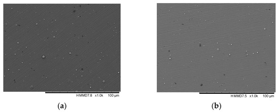
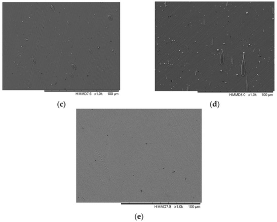
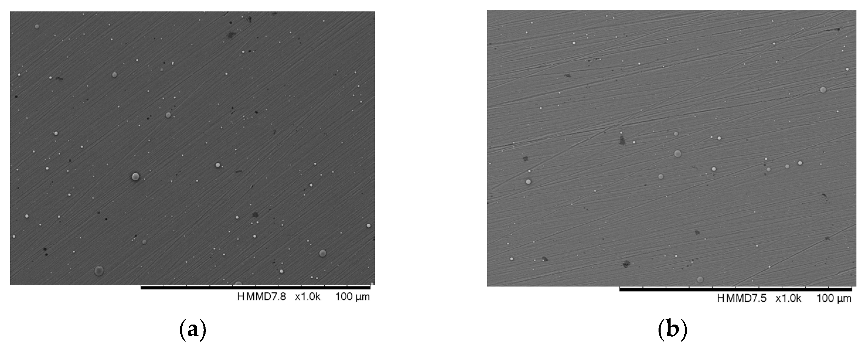
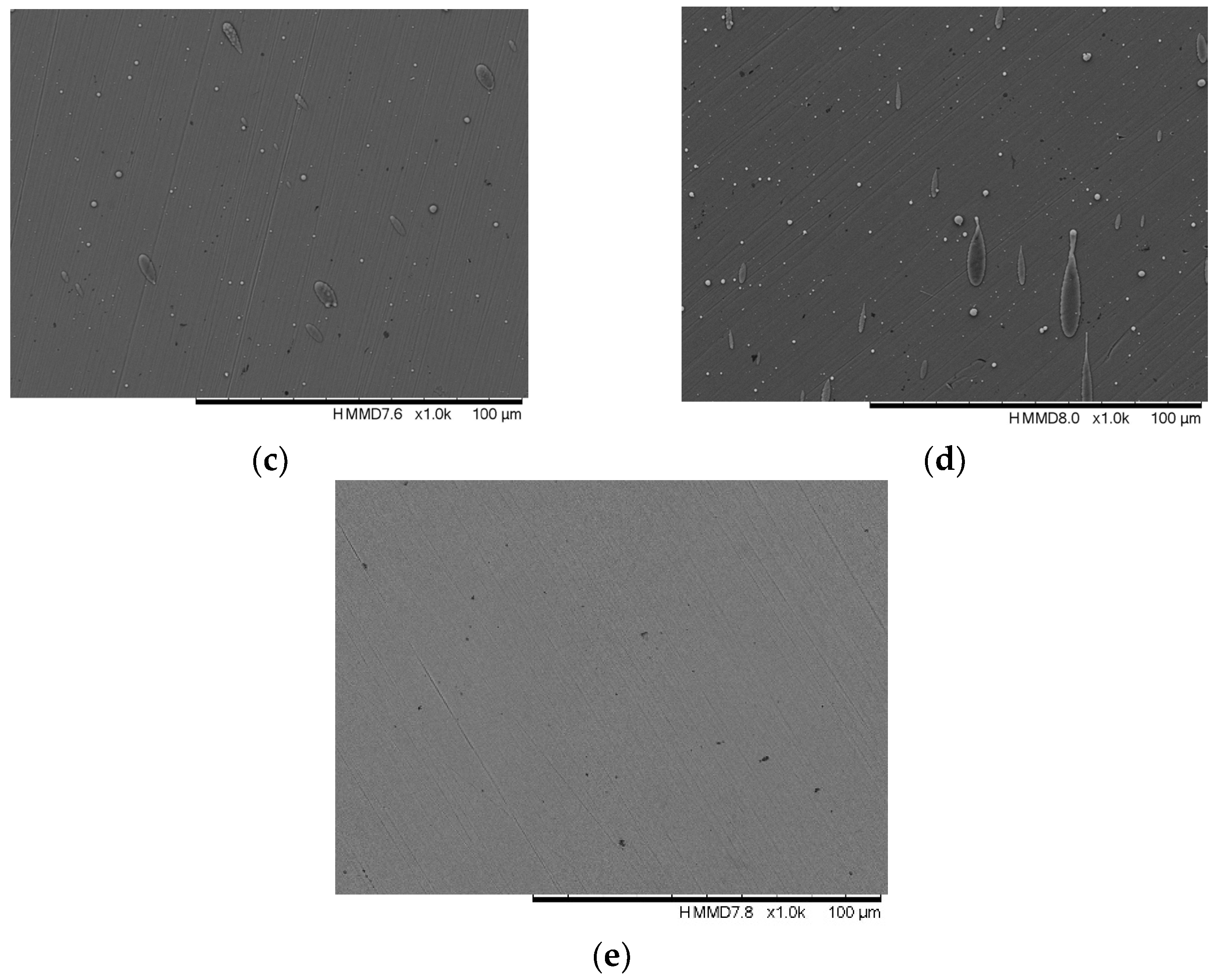
Figure 5 presents SEM images at 1000× magnification of the Ti-coated 316L surfaces, showing the presence of microdroplets characteristic of unfiltered cathodic arc evaporation. For the samples deposited at normal incidence (0°), both at 65 A and 90 A, the droplets exhibit predominantly spherical shapes with relatively symmetric footprints, indicating rapid solidification upon impact on a trajectory nearly perpendicular to the substrate. However, for films deposited at an oblique angle of 80°, the droplet morphology changes: in addition to nearly spherical droplets, elongated droplets frequently appear, aligned with the direction of the incoming particle flux. This morphology results from the combination of the oblique deposition geometry and the thermal state of the material ejected from the Ti cathode. Droplets that reach the substrate at higher temperatures retain mobility for a short time after impact, allowing them to deform and elongate before solidifying. At the same time, cooler droplets preserve a more symmetric shape. These shape and orientation differences observed in the 80° films provide insight into the local solidification conditions and the influence of OAD geometry on the final microstructure of the coating, with a direct impact on roughness and, consequently, on the optical properties.
Figure 5.
SEM images at 1000× magnification of the Ti-coated 316L surfaces as a function of incidence angle and arc current: (a) 316L/Ti 0°, I = 65 A; (b) 316L/Ti 0°, I = 90 A; (c) 316L/Ti 80°, I = 65 A; (d) 316L/Ti 80°, I = 90 A; (e) 316L substrate.
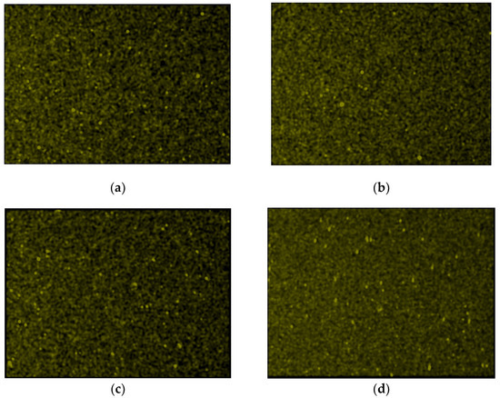
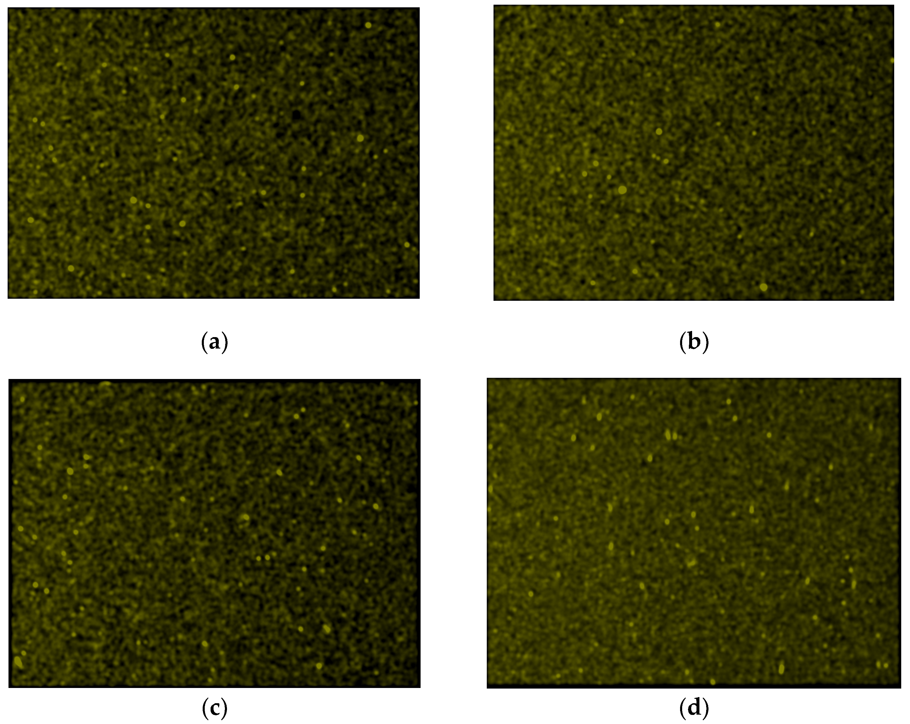
The Ti EDS elemental maps (Figure 6) at 100× magnification confirm that all deposited coatings form a continuous Ti layer on the 316L substrate, regardless of the incidence angle (0° or 80°) or arc current (65 A or 90 A). For all deposition conditions, Ti is uniformly distributed across the scanned area, with only minor intensity fluctuations, indicating no Ti-depleted regions or uncovered substrate areas at the investigated microscale.
Figure 6.
EDS Ti elemental maps at 100× magnification (HV: 15 kV, WD: 7.6 mm) of the Ti-coated 316L surfaces as a function of incidence angle and arc current: (a) 316L/Ti 0°, I = 65 A; (b) 316L/Ti 0°, I = 90 A; (c) 316L/Ti 80°, I = 65 A; (d) 316L/Ti 80°, I = 90 A.
The brighter spots visible in the maps correspond to the microdroplets identified in the SEM images and exhibit Ti intensities comparable to or higher than the surrounding matrix. This confirms that the droplets are Ti-rich entities produced by the cathodic arc process, rather than defects that expose the steel substrate or incorporate foreign contaminants. Comparing normal and oblique incidence, as well as 65 A and 90 A, no large-scale segregation or clustering of Ti is observed, which suggests that changes in current and incidence angle primarily affect droplet size and surface morphology rather than the overall uniformity of Ti coverage.
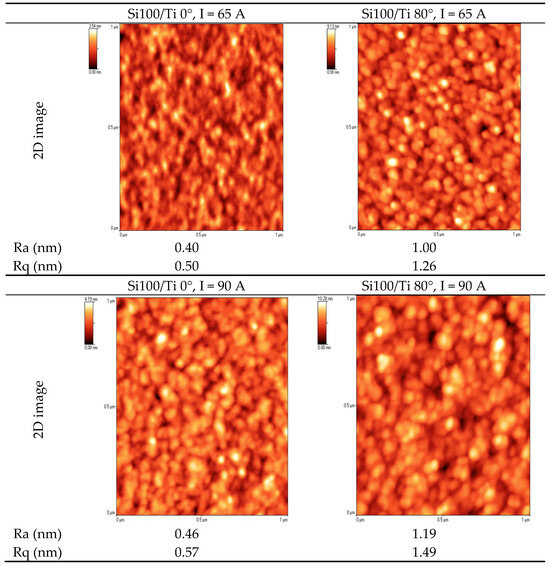
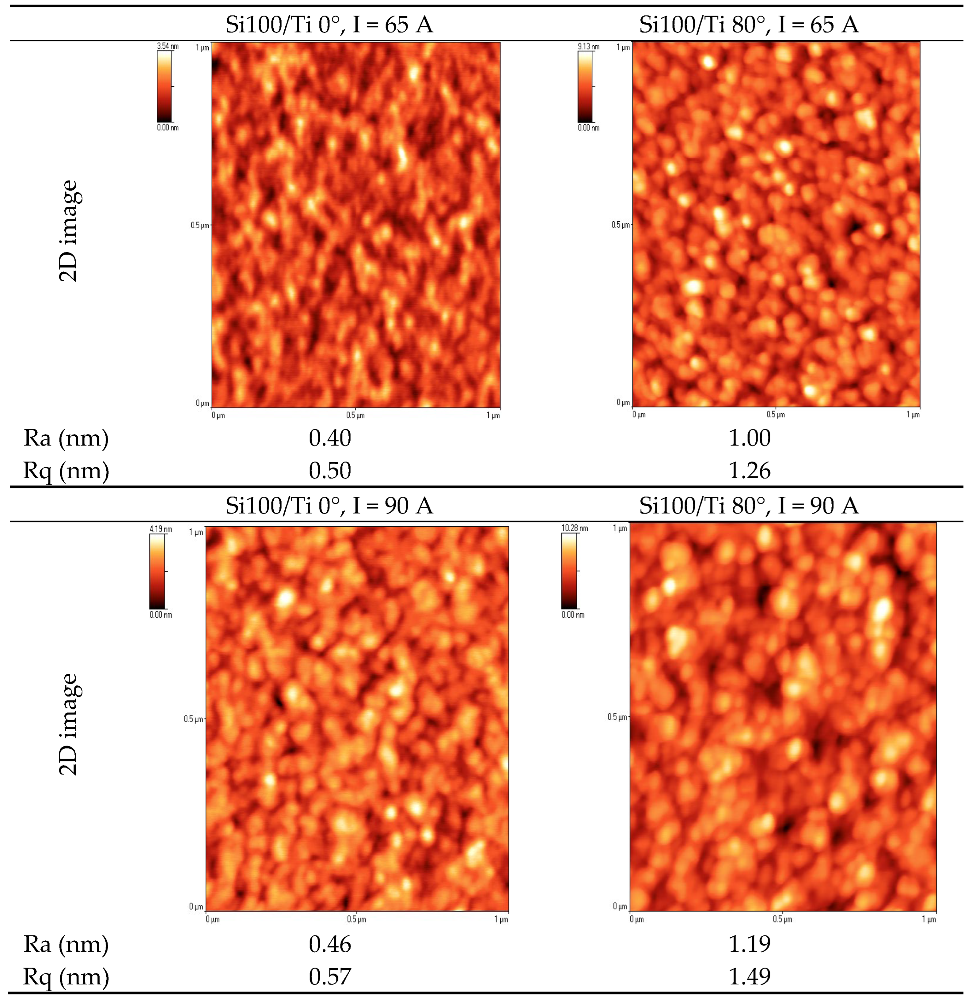
The AFM images in Figure 7 show that Ti films deposited at normal incidence (0°) exhibit a very smooth surface, with Ra ~0.40–0.46 nm and Rq ~0.50–0.57 nm, indicating a continuous, homogeneous layer. However, the films deposited at 80° exhibit pronounced surface texturing, with roughness increasing by approximately a factor of 2 (Ra ~1.00–1.19 nm, Rq ~1.26–1.49 nm). This increase in roughness is consistent with the SEM observations, which show elongated features and possible self-shadowing effects characteristic of oblique-angle deposition. It supports the hypothesis that OAD geometry results in a more textured surface. The Ti films deposited at normal incidence (0°) on Si(100) show a compact, fine-grained morphology, with small, closely packed hillocks and valleys confirming the deposition of a thin, continuous film.
Figure 7.
AFM images of the Ti film surfaces deposited on Si(100) substrates at 0° and 80°, with ITi = 65 A and 90 A.
For the films deposited at 80°, the topography becomes visibly more textured. The bright features are larger and more elongated, and the contrast between high and low areas is stronger. This gives the surface a more pronounced, “corrugated” appearance, with local features that tend to be slightly aligned, consistent with the oblique arrival of the Ti vapor flux. Note that the area scanned by AFM is significantly smaller than the one visible in the SEM images. Therefore, the features observed and the roughness correspond to the continuous Ti layer observed between the droplets in the SEM images.
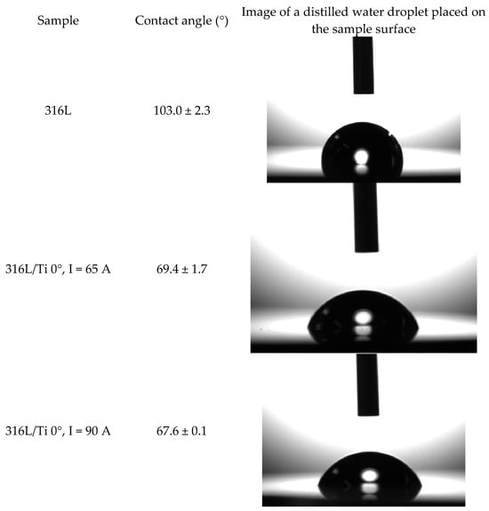
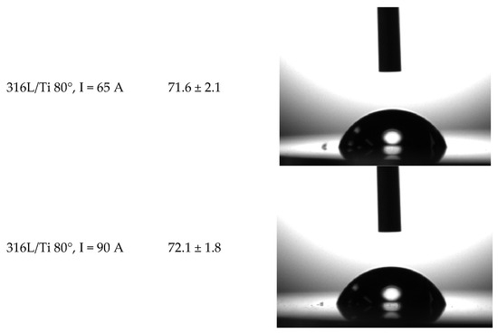
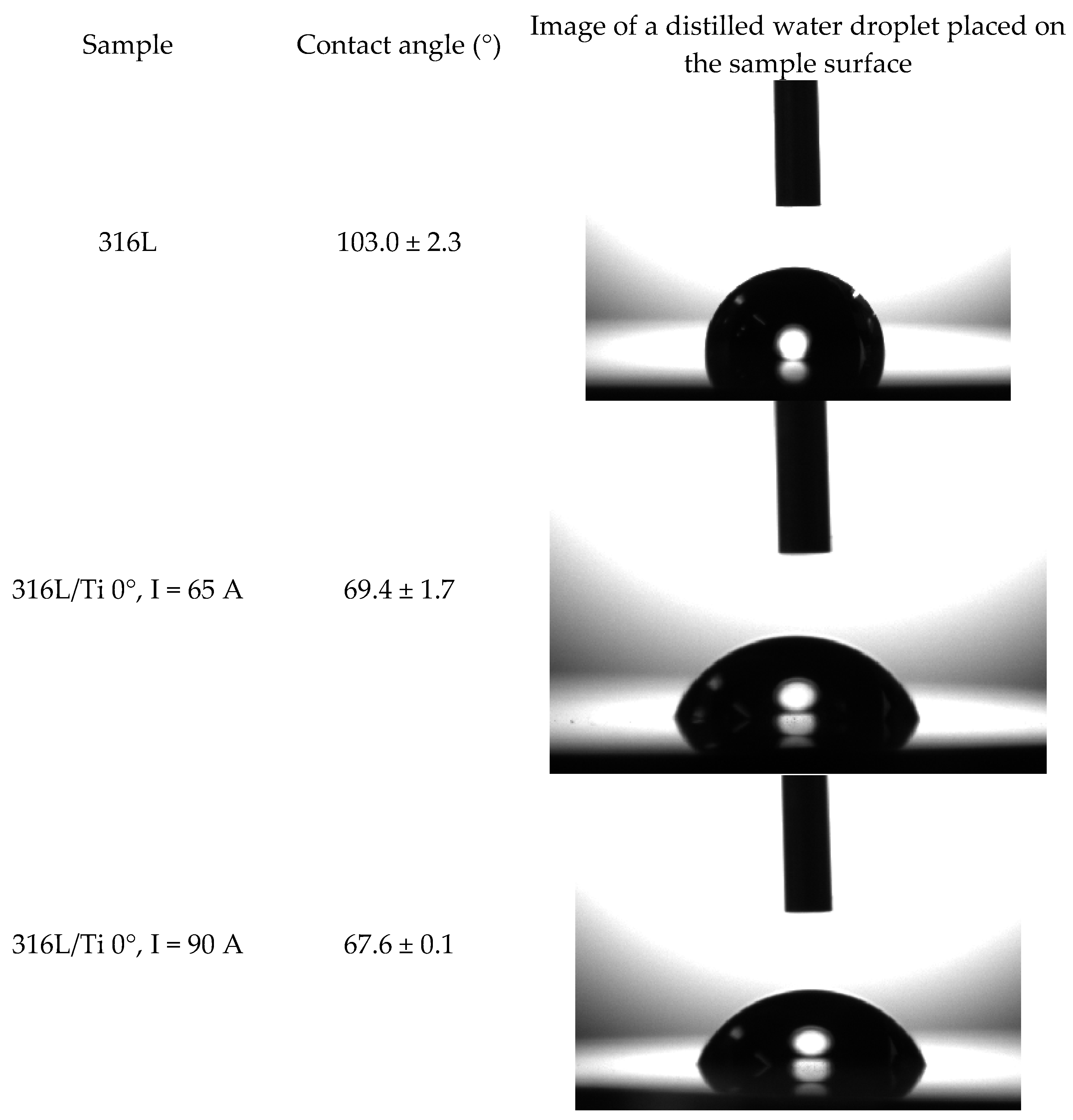
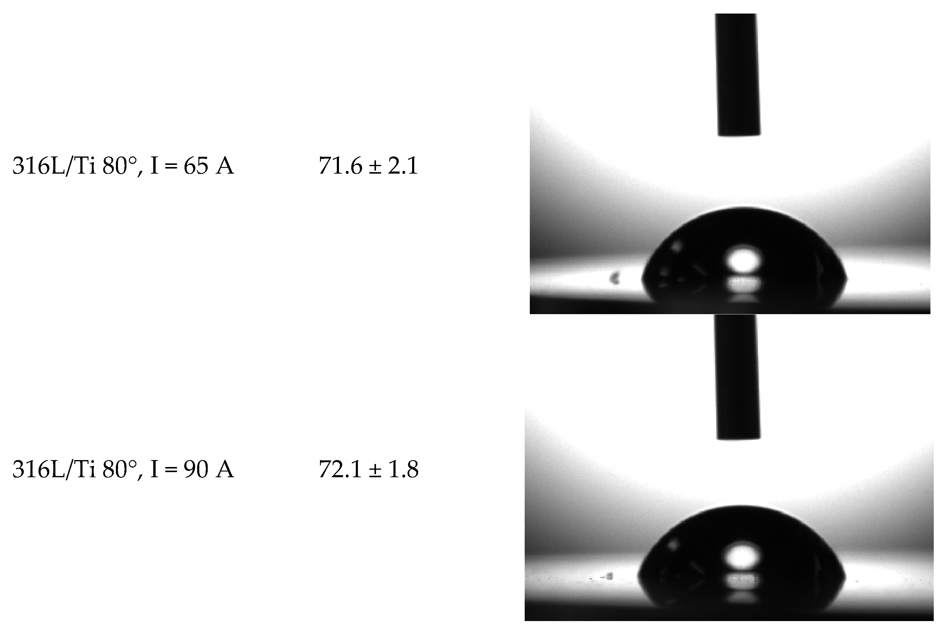
The contact angle measurement results are presented in Figure 8, showing a transition from the hydrophobic behavior of the bare 316L substrate to a more moderate, hydrophilic character for the Ti-coated surfaces. The differences between the samples deposited at 0° and 80°, as well as between 65 A and 90 A, are relatively small and lie within the experimental uncertainty. Films deposited at 0° are slightly more wettable, whereas coatings deposited at 80° exhibit contact angles that are about 2–4° higher, consistent with the increased roughness observed by AFM. Overall, the results indicate that the deposition of a single Ti layer significantly alters the surface character compared with bare 316L. At the same time, variations in process parameters have only a secondary influence on wettability. Because roughness affects apparent wettability, the contact angle results reported here are compared only within the same substrate type (316L), so that differences reflect coating-growth conditions rather than substrate-to-substrate variations.
Figure 8.
Contact angle values for a distilled water droplet placed on the surface of the 316L substrate and on the Ti films deposited at 0° and 80°, for ITi = 65 A and 90 A.
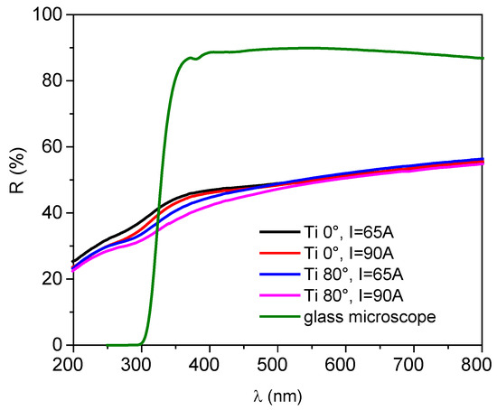
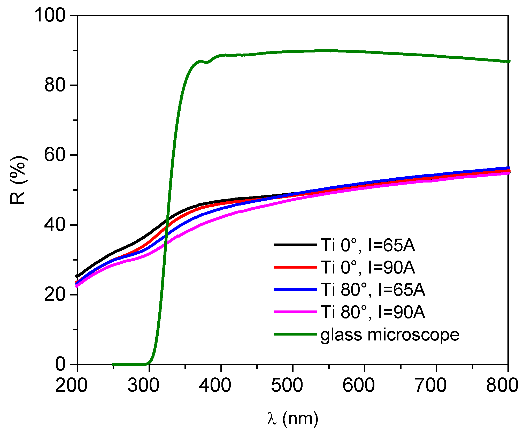
The optical analysis revealed that in the visible spectral range (~400–800 nm), all Ti thin films deposited on 1 mm-thick microscope glass exhibit a lower reflectance than the bare glass substrate (Figure 9). Analysis of the reflectance spectra shows that depositing a ~100 nm Ti layer reduces reflectance in the UV-Vis range and increases the solar absorption coefficient. In addition, oblique-angle deposition (80°) showed the highest anti-reflective character among the investigated metallic films, in agreement with the increased surface texturing observed by AFM.
Figure 9.
Reflectance spectra in the UV–Vis range obtained for Ti thin films deposited on microscope glass substrate.
4. Discussion
The present study examined the influence of incidence angle and arc current on the structure, morphology, composition, surface properties, and optical response of Ti thin films deposited by unfiltered cathodic arc evaporation. Because cathodic arc plasmas differ fundamentally from the low-energy vapor fluxes typically employed in OAD research (thermal evaporation, magnetron sputtering, IBS, PLD), the results provide new insights into how energetic ion–assisted growth modifies classical oblique-angle deposition mechanisms. The combined GIXRD, SEM/EDS, AFM, wettability, and optical measurements reflect the interplay among geometric shadowing, ion-induced densification/defect formation, and microdroplets generated intrinsically by the arc process. Substrate characteristics, including surface condition, nucleation behavior, and thermal-mechanical mismatch, can influence film growth. Therefore, the microstructural evidence and optical properties presented here should be interpreted in relation to the specific substrate used for each measurement. In this study, we emphasize the effects of deposition angle and arc current as key process parameters. Consequently, the conclusions presented are specific to each substrate.
Among all samples, the film deposited at 0° and 65 A exhibits the most intense and well-defined reflections, corresponding to c-TiO(111) and indicating a higher degree of crystallinity. With the cathodic current increased to 90 A, the GIXRD peaks become broader and less intense, suggesting a more disordered microstructure, which may be related to the higher energy of the incident particle flux and to the increased oxygen content revealed by the EDS analysis. As a secondary observation, some diffraction maxima are slightly shifted toward higher 2θ angles compared with their standard positions. This behavior can be consistent with growth-related lattice distortion (e.g., compressive stress [32] and/or point-defect incorporation) promoted by ion bombardment in an OAD-CAE process [23], and it may also be affected by interstitial oxygen in hcp Ti [33].
AFM analyses indicate that the microstructure transitions from fine, isotropic grains at 0° to more textured, elongated features at 80°. However, unlike sputtered OAD films, which form well-separated columns at extreme angles [34], CAE films remain relatively compact, highlighting the role of higher-energy ions, which enhance adatom mobility and partially suppress extreme columnar porosity. One of the significant differences between CAE and all other PVD processes is the generation of molten droplets and particulates ejected from the cathode [35]. The presence of Ti-rich droplets is clearly observed in both SEM images and EDS maps, which show bright zones. The droplet density increases slightly with higher arc currents, while elongated droplets are specifically formed only at a deposition angle of 80°. This observation suggests that the angle of deposition influences not only droplet morphology but also their distribution and shape, highlighting the effects of process parameters on Ti coating characteristics. These observations agree with the established arc-cathode-spot behavior, where higher arc currents increase spot velocity and ejection rate [36]. Microdroplets also affect the oxidation state at the sample’s surface [37], roughness (especially at 90 A), and optical scattering, all of which contribute to the antireflective behavior observed at 80°. EDS analysis confirms Ti and O as the main constituents of the deposited thin films. Although EDS penetration exceeds their thickness, the observed oxygen trends indicate that O content increases at 90 A (both angles), while higher roughness correlates with higher O content. Recent reports on arc-deposited Ti films also confirm that wettability is dominated by native TiOx chemistry and nanoscale roughness [38]. All Ti coatings reduce UV-visible-range reflectance relative to bare glass, thereby increasing absorptance, which is highly desirable for solar thermal applications. OAD Ti films exhibit even lower reflectance due to increased light trapping arising from surface texturing, along with antireflective behavior induced by nano- and microscale roughness. While bare Ti coating is not a complete solar-selective absorber [39,40], its observed properties (tunable roughness, the ability to generate a TiOx passive layer to protect against moderate temperatures, compatibility with nitride/oxynitride/oxide top layers) meet the key requirements for advanced multilayer absorber stacks.
5. Conclusions
In this work, Ti thin films were deposited by unfiltered cathodic arc evaporation at two incidence angles (0° and 80°) and two arc currents (65 A and 90 A) on 316L stainless steel, Si(100), and microscope glass substrates to evaluate how deposition geometry and plasma conditions affect film structure and optical response. The calculated deposition rate decreases at high incidence angle (80°) due to the reduced projected collection area and geometric shadowing associated with oblique-angle deposition. Increasing the arc current further reduces the apparent deposition rate, consistent with stronger energetic bombardment and enhanced re-emission/self-sputtering. SEM reveals the characteristic arc-generated droplet population. At oblique incidence, droplets more frequently display elongated footprints aligned with the incoming flux direction, and the nanoscale roughness increases, consistent with OAD-driven surface development. Conventional 2θ/θ scans are largely featureless for most samples due to their thinness/low crystallinity, whereas GiXRD identifies nanocrystalline α-Ti, a cubic TiO component, and texture through relative peak intensities; the 0°/65 A condition shows the highest crystallinity. The reflectance response in the ultraviolet and visible ranges varies with deposition angle and arc current, indicating that microstructural differences induced by growth conditions can be used to tailor the optical performance of Ti coatings. Because different substrates were used to support specific characterization methods (optical measurements on microscope glass slides, AFM/GIXRD on Si100, and wettability/SEM/EDS on 316L stainless steel discs), the absolute values are substrate-specific, and extrapolation to other substrates should be performed with careful consideration. These results demonstrate that deposition angle and arc current provide practical control for tuning the morphology, nanostructure, and optical response of Ti coatings grown by cathodic arc evaporation.
Author Contributions
Conceptualization, I.P. and C.V.; data curation, A.C.P., N.C.Z., M.D. and I.P.; formal analysis, A.E.K., N.C.Z. and L.R.C.; investigation, A.C.P., I.P. and M.D.; methodology, A.E.K., and L.R.C.; resources, A.V. and L.R.C.; supervision, I.P. and C.V.; validation, M.D., A.E.K. and A.V.; Writing—original draft, I.P. and C.V.; Writing—review and editing, I.P., M.D., N.C.Z., A.V. and C.V. All authors have read and agreed to the published version of the manuscript.
Funding
This work was supported by a grant of the Ministry of Research, Innovation and Digitization, CCCDI–UEFISCDI, project number PN-IV-P8-8.3-PM-RO-TR-2024-0065, within PNCDI IV (contract 1BMTR/2025).
Data Availability Statement
The original contributions presented in this study are included in the article. Further inquiries can be directed to the corresponding author.
Acknowledgments
INOE research was funded by the Romanian Ministry of Research, Innovation and Digitalization through the National Research Development and Innovation Plan 2022–2027, Core Program, project number PN 23 05, contract number PN11N-03-01-2023.
Conflicts of Interest
The authors declare no conflicts of interest. The funders had no role in the study’s design, in the collection, analyses, or interpretation of data; in the writing of the manuscript; or in the decision to publish the results.
References
- Kalogirou, S.A. Solar thermal collectors and applications. Prog. Energy Combust. Sci. 2004, 30, 231–295. [Google Scholar] [CrossRef] [Scilit]
- Phani Kumar, K.K.; Atchuta, S.R.; Shiva Prasad, M.; Barshilia, H.C.; Sakthivel, S. Review on selective absorber coatings: A catalyst for enhanced solar energy conversion efficiency. Sol. Energy Mater. Sol. Cells 2024, 277, 113080. [Google Scholar] [CrossRef] [Scilit]
- Kumar, Y.; Kumar, S.; Verma, P. Role of absorber and glazing in thermal performance improvements of liquid flat plate solar collector: A review. Energy Sources, Part A Recover. Util. Environ. Eff. 2023, 45, 10802–10826. [Google Scholar] [CrossRef] [Scilit]
- Bassam, N. El Solar energy: Technologies and options. In Distributed Renewable Energies for Off-Grid Communities: Empowering a Sustainable, Competitive, and Secure Twenty-First Century, 2nd ed.; Elsevier: Amsterdam, The Netherlands, 2021; pp. 123–147. [Google Scholar] [CrossRef] [Scilit]
- Yang, J.; Shen, H.; Yang, Z.; Zhao, Q. Hybrid-structured air-stable solar selective absorber on flexible textured silicon. Sol. Energy 2022, 231, 837–845. [Google Scholar] [CrossRef] [Scilit]
- Kong, L.; Fan, D.W.; Wang, W.; Wang, C. Spectral properties and microstructure of sputtered WOx films for solar conversion applications. Surf. Interface Anal. 2020, 52, 407–412. [Google Scholar] [CrossRef] [Scilit]
- Shah, A.A.; Gupta, M.C. Spectral selective surfaces for concentrated solar power receivers by laser sintering of tungsten micro and nano particles. Sol. Energy Mater. Sol. Cells 2013, 117, 489–493. [Google Scholar] [CrossRef] [Scilit]
- Selvakumar, N.; Santhoshkumar, S.; Basu, S.; Biswas, A.; Barshilia, H.C. Spectrally selective CrMoN/CrON tandem absorber for mid-temperature solar thermal applications. Sol. Energy Mater. Sol. Cells 2013, 109, 97–103. [Google Scholar] [CrossRef] [Scilit]
- Wang, C.; Li, W.; Li, Z.; Fang, B. Solar thermal harvesting based on self-doped nanocermet: Structural merits, design strategies and applications. Renew. Sustain. Energy Rev. 2020, 134, 110277. [Google Scholar] [CrossRef] [Scilit]
- Atchuta, S.R.; Sakthivel, S.; Barshilia, H.C. Transition metal based CuxNiyCoz-x-yO4 spinel composite solar selective absorber coatings for concentrated solar thermal applications. Sol. Energy Mater. Sol. Cells 2019, 189, 226–232. [Google Scholar] [CrossRef] [Scilit]
- Kant, K.; Sibin, K.P.; Pitchumani, R. Novel fractal-textured solar absorber surfaces for concentrated solar power. Sol. Energy Mater. Sol. Cells 2022, 248, 112010. [Google Scholar] [CrossRef] [Scilit]
- Sani, E.; Sciti, D.; Silvestroni, L.; Bellucci, A.; Orlando, S.; Trucchi, D.M. Tailoring optical properties of surfaces in wide spectral ranges by multi-scale femtosecond-laser texturing: A case-study for TaB2 ceramics. Opt. Mater. 2020, 109, 110347. [Google Scholar] [CrossRef] [Scilit]
- Jose, S.A.; John, M.; Menezes, P.L. Cermet Systems: Synthesis, Properties, and Applications. Ceramics 2022, 5, 210–236. [Google Scholar] [CrossRef] [Scilit]
- Kolokytha, C.; Lathiotakis, N.N.; Kaltzoglou, A.; Petsalakis, I.D.; Tzeli, D. The Effect of A-Cation and X-Anion Substitutions on the Electronic and Structural Properties of A2ZrX6 ‘Defect’ Perovskite Materials: A Theoretical Density Functional Theory Study. Materials 2025, 18, 726. [Google Scholar] [CrossRef] [Scilit]
- Yang, X.; Qin, X.; Yan, W.; Zhang, C.; Zhang, D. Effects of Mn and Co Doping on the Electronic Structure and Optical Properties of Cu2ZnSnS4. Crystals 2025, 15, 781. [Google Scholar] [CrossRef] [Scilit]
- Ouaaka, E.; Aazza, M.; Bouymajane, A.; Cacciola, F. Electronic, Optical, Thermoelectric and Elastic Properties of RbxCs1−xPbBr3 Perovskite. Molecules 2023, 28, 2880. [Google Scholar] [CrossRef] [Scilit] [PubMed]
- Lacroix, B.; Paumier, F.; Santos, A.J.; Maudet, F.; Girardeau, T.; Dupeyrat, C.; García, R.; Morales, F.M. Texture in ITO films deposited at oblique incidence by ion beam sputtering. Appl. Surf. Sci. 2022, 605, 154677. [Google Scholar] [CrossRef] [Scilit]
- Dalapati, G.K.; Masudy-Panah, S.; Chua, S.T.; Sharma, M.; Wong, T.I.; Tan, H.R.; Chi, D. Color tunable low cost transparent heat reflector using copper and titanium oxide for energy saving application. Sci. Rep. 2016, 6, 20182. [Google Scholar] [CrossRef] [Scilit]
- Pana, I.; Vitelaru, C.; Kiss, A.; Zoita, N.C.; Dinu, M.; Braic, M. Design, fabrication and characterization of TiO2-SiO2 multilayer with tailored color glazing for thermal solar collectors. Mater. Des. 2017, 130, 275–284. [Google Scholar] [CrossRef] [Scilit]
- Sadeghi-Khosravieh, S.; Robbie, K. Morphology and crystal texture in tilted columnar micro-structured titanium thin film coatings. Thin Solid Films 2017, 627, 69–76. [Google Scholar] [CrossRef] [Scilit]
- Dervaux, J.; Cormier, P.A.; Moskovkin, P.; Douheret, O.; Konstantinidis, S.; Lazzaroni, R.; Lucas, S.; Snyders, R. Synthesis of nanostructured Ti thin films by combining glancing angle deposition and magnetron sputtering: A joint experimental and modeling study. Thin Solid Films 2017, 636, 644–657. [Google Scholar] [CrossRef] [Scilit]
- Bordbari, M.; Eshraghi, M.J.; Naderi, N.; Sedaghat Ahangari Hossein Zadeh, A. Investigation of structural and optical properties of oblique angle sputter deposited barium strontium titanate nanostructures. Mater. Res. Express 2019, 6, 025009. [Google Scholar] [CrossRef] [Scilit]
- Barranco, A.; Borras, A.; Gonzalez-Elipe, A.R.; Palmero, A. Perspectives on oblique angle deposition of thin films: From fundamentals to devices. Prog. Mater. Sci. 2016, 76, 59–153. [Google Scholar] [CrossRef] [Scilit]
- Jain, R.K.; Kaur, J.; Arora, S.; Kumar, A.; Chawla, A.K.; Khanna, A. Effects of oblique angle deposition on structural, electrical and wettability properties of Bi thin films grown by thermal evaporation. Appl. Surf. Sci. 2019, 463, 45–51. [Google Scholar] [CrossRef] [Scilit]
- Eriksson, A.O.; Zhirkov, I.; Dahlqvist, M.; Jensen, J.; Hultman, L.; Rosen, J. Characterization of plasma chemistry and ion energy in cathodic arc plasma from Ti-Si cathodes of different compositions. J. Appl. Phys. 2013, 113, 163304. [Google Scholar] [CrossRef] [Scilit]
- Patel, U.; Rawal, S.; Bose, B.; Arif, A.F.M.; Veldhuis, S. Performance evaluations of Ti-based PVD coatings deposited on cermet tools for high-speed dry finish turning of AISI 304 stainless steel. Wear 2022, 492–493, 204214. [Google Scholar] [CrossRef] [Scilit]
- Haubner, R.; Lessiak, M.; Pitonak, R.; Köpf, A.; Weissenbacher, R. Evolution of conventional hard coatings for its use on cutting tools. Int. J. Refract. Met. Hard Mater. 2017, 62, 210–218. [Google Scholar] [CrossRef] [Scilit]
- Kivaisi, R.T. Optical properties of selectively absorbing chromium films deposited at oblique angle of incidence. Sol. Energy Mater. 1981, 5, 115–127. [Google Scholar] [CrossRef] [Scilit]
- Lee, G.; Ko, R.; Kang, S.; Kim, Y.J.; Kim, Y.-J.; Yoo, H. Nanostructure Engineering by Oblique Angle Deposition for Photodetectors and Other Applications. Micromachines 2025, 16, 865. [Google Scholar] [CrossRef] [Scilit]
- Alami, J.; Sarakinos, K.; Mark, G.; Wuttig, M. On the deposition rate in a high power pulsed magnetron sputtering discharge. Appl. Phys. Lett. 2006, 89, 154104. [Google Scholar] [CrossRef] [Scilit]
- Cullity, B.D.; Stock, S.R. (Eds.) Elements of X-Ray Diffraction; Pearson: Harlow, UK, 2014; ISBN 9781292052557. [Google Scholar]
- Chu, J.; Peng, X.; Sajjad, M.; Yang, B.; Feng, P.X. Nanostructures and sensing properties of ZnO prepared using normal and oblique angle deposition techniques. Thin Solid Film. 2012, 520, 3493–3498. [Google Scholar] [CrossRef] [Scilit]
- Guo, S.; Liu, C.T. Phase stability in high entropy alloys: Formation of solid-solution phase or amorphous phase. Prog. Nat. Sci. Mater. Int. 2011, 21, 433–446. [Google Scholar] [CrossRef] [Scilit]
- Lopez-Santos, C.; Alvarez, R.; Garcia-Valenzuela, A.; Rico, V.; Loeffler, M.; Gonzalez-Elipe, A.R.; Palmero, A. Nanocolumnar association and domain formation in porous thin films grown by evaporation at oblique angles. Nanotechnology 2016, 27, 395702. [Google Scholar] [CrossRef] [Scilit]
- Sebastiani, M.; Piccoli, M.; Bemporad, E. Effect of micro-droplets on the local residual stress field in CAE-PVD thin coatings. Surf. Coatings Technol. 2013, 215, 407–412. [Google Scholar] [CrossRef] [Scilit]
- Beilis, I.I. The Phenomenon of a Cathode Spot in an Electrical Arc: The Current Understanding of the Mechanism of Cathode Heating and Plasma Generation. Plasma 2024, 7, 329–354. [Google Scholar] [CrossRef] [Scilit]
- Koller, C.M.; Kirnbauer, A.; Dalbauer, V.; Kolozsvári, S.; Ramm, J.; Mayrhofer, P.-H. On the oxidation behavior of cathodic arc evaporated Al-Cr-Fe and Al-Cr-Fe-O coatings. I. J. Vac. Sci. Technol. A Vac. Surf. Film. 2019, 37, 041503. [Google Scholar] [CrossRef] [Scilit]
- Terlicka, S.; Sobczak, N.; Maj, Ł.; Darłak, P.; Sobczak, J.J. Wettability, reactivity, and interface structure in Mg/Ni system. J. Magnes. Alloy. 2024, 12, 659–672. [Google Scholar] [CrossRef] [Scilit]
- Chen, P.; Yi, Y.; Song, Q.; Yi, Z.; Yi, Y.; Cheng, S.; Zhang, J.; Tang, C.; Sun, T.; Zeng, Q. Simulation and Analysis of a Near-Perfect Solar Absorber Based on SiO2-Ti Cascade Optical Cavity. Photonics 2024, 11, 604. [Google Scholar] [CrossRef] [Scilit]
- Lai, F.-D.; Li, W.-Y. Design, Fabrication and Analysis for Al2 O3 /Ti/Al2 O3 Colored Solar Selective Absorbers for Building Applications. Coatings 2022, 12, 521. [Google Scholar] [CrossRef] [Scilit]
Disclaimer/Publisher’s Note: The statements, opinions and data contained in all publications are solely those of the individual author(s) and contributor(s) and not of MDPI and/or the editor(s). MDPI and/or the editor(s) disclaim responsibility for any injury to people or property resulting from any ideas, methods, instructions or products referred to in the content. |
© 2026 by the authors. Licensee MDPI, Basel, Switzerland. This article is an open access article distributed under the terms and conditions of the Creative Commons Attribution (CC BY) license.