


Abstract
SnO2 exhibits low cost, high electron mobility and good optical transparency, making it a promising candidate for the active layer of indium-free oxide thin-film transistors (TFTs). However, its film qualities are highly sensitive to deposition conditions. In this work, SnO2 thin films and TFTs were fabricated by radio-frequency magnetron sputtering under different substrate biases (0 V, −70 V and −110 V) to investigate the effects of substrate bias on film structure, defect state, interface quality and device performance. With increasing substrate bias magnitude, the film crystallinity improved, the relative area fraction of the defect-related O 1s component decreased from 31% to 19%, while the surface roughness increased, continuously. At a substrate bias of −70 V, the device exhibited relatively optimal overall performance, with a linear mobility (μlin) of 3.7 cm2/Vs, a subthreshold swing (SS) of 0.61 V/dec, and a threshold-voltage shift (ΔVth) of 6.0 V after 3600 s of positive bias stress. These results indicate that an appropriate substrate bias can achieve a balance between crystalline quality and interface condition, thereby improving the performance of SnO2 TFTs.
1. Introduction
Metal-oxide thin-film transistors (TFTs) have considerable potential for next-generation flat-panel displays, transparent electronics, and large-area sensor arrays because of their relatively high carrier mobility, good optical transparency, and compatibility with low-temperature, large-area fabrication processes [1,2,3]. Among oxide semiconductors, SnO2 is regarded as a competitive active-layer material for TFTs due to its wide band gap, high visible-light transmittance, good chemical stability, and the cost advantage of being indium-free. Nevertheless, the electrical behavior of SnO2 is highly sensitive to oxygen-related defects. Donor-like defects such as oxygen vacancies can produce an excessively high electron concentration, shift the threshold voltage in the negative direction, and prevent complete device turn-off. Moreover, channel carriers are transported primarily near the active-layer/gate-dielectric interface, where surface roughness and interface traps may cause carrier scattering, charge trapping, and bias-stress instability. Simultaneous control of bulk defects and interface quality is therefore essential for realizing high-performance SnO2 TFTs [4,5,6,7].
Substrate bias has been employed to regulate the properties of magnetron-sputtered oxide films. An appropriate negative bias can enhance ion bombardment and adatom mobility, promoting film densification and structural ordering, whereas excessive bombardment may induce re-sputtering, structural defects, and morphological changes [8,9,10,11]. Such effects have been investigated in various oxides, including ZnO, ITO, TiO2, Al2O3, HfO2, and NiO [12,13,14,15,16,17,18,19]. For SnO2, Prathyusha et al. demonstrated that substrate bias modifies the crystalline structure and optoelectronic properties of the films [20]. Bias-assisted sputtering has also been applied to oxide TFT channel layers to regulate device characteristics [21]. However, these findings do not fully clarify whether bias-induced improvements in SnO2 film structure translate into better transistor performance, particularly when changes in oxygen-related chemical environments and surface morphology occur simultaneously. The associated trade-offs in carrier transport and bias-stress stability therefore require further investigation.
In this work, SnO2 films and the TFTs were fabricated by radio-frequency magnetron sputtering at substrate biases of 0 V, −70 V, and −110 V, respectively. Structural, morphological, chemical-state, optical, and electrical measurements were combined to examine the relationships between bias-induced film modifications and transistor characteristics.
The results reveal that enhanced crystallinity and a reduced defect-related O 1s component are accompanied by increased surface roughness and decreased field-effect mobility. The −70 V device retains relatively high mobility while exhibiting improved positive bias stress (PBS) stability compared with the unbiased device. These findings clarify the competing effects and practical trade-offs of substrate-bias regulation in SnO2 TFTs, and they provide guidance for selecting suitable deposition conditions.
2. Experimental Methods
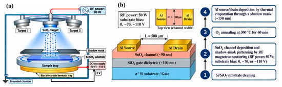
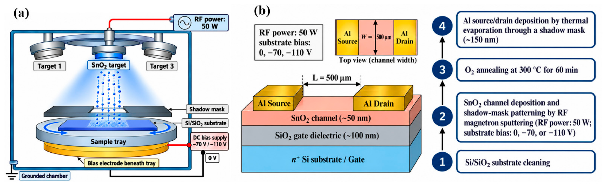
SnO2 films with a thickness of approximately 50 nm were deposited by radio-frequency magnetron sputtering using a high-vacuum multi-target deposition system (JCPY600) and a 99.99–pure SnO2 ceramic target. Si/SiO2 substrates (~100 nm SiO2) were sequentially ultrasonicated in acetone, ethanol, and deionized water for 10 min each and dried with nitrogen. The base and working pressures were 5 × 10⁻⁴ and 0.3 Pa, respectively, with a fixed radio frequency (RF) power of 50 W and Ar/O2 flow rate of 10 sccm/40 sccm. Substrate biases of 0 V, −70 V, and −110 V were applied while the other parameters remain unchanged. The substrate bias was applied during SnO2 deposition by DC bias power, which connects to the bias electrode beneath the sample holder, as shown in Figure 1a. The channel films were annealed in O2 at 300 °C for 60 min, followed by thermal evaporation of ~150 nm Al source/drain electrodes to form top source/drain electrodes. All the channels and top electrodes were patterned by a shadow mask with channel width (W)/length (L) = 500 µm/500 µm. The fabricated device structure and the main preparation process are shown in Figure 1b.
Figure 1.
Schematics of (a) substrate-bias configuration used for SnO2 deposition; (b) device structure and the main preparation process.
Phase structure was analyzed using a grazing-incidence X-ray diffractometer (GIXRD, Bruker D8 ADVANCE, Karlsruhe, Germany) with 2θ = 20–80°, step size 0.02°, scan rate 2°/min, and incidence angle 0.6°. Surface morphology and root-mean-square roughness were examined using a scanning electron microscope (SEM, Helios 5 CX, Hillsboro, OR, USA) and an atomic force microscope (AFM, Bruker Dimension Icon, Billerica, MA, USA), respectively. The elemental composition and chemical states of the films were analyzed using an X-ray photoelectron spectrometer (XPS, Thermo Scientific K-Alpha, Waltham, MA, USA) with Al Kα radiation. Optical transmittance in the range of 300 nm–800 nm was measured using a spectrophotometer (Agilent Cary 5000, Santa Clara, CA, USA). The transfer characteristics, output characteristics and the device stabilities were measured using a probe station (CINDBEST CS-4, Shenzhen, China) and a dual-channel source meter (Keithley 2636B, Cleveland, OH, USA).
3. Results and Discussion
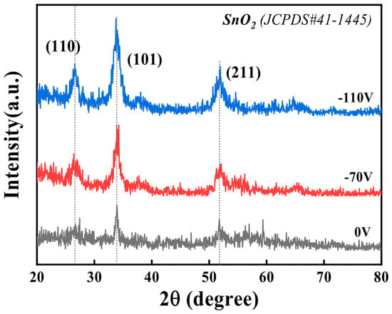
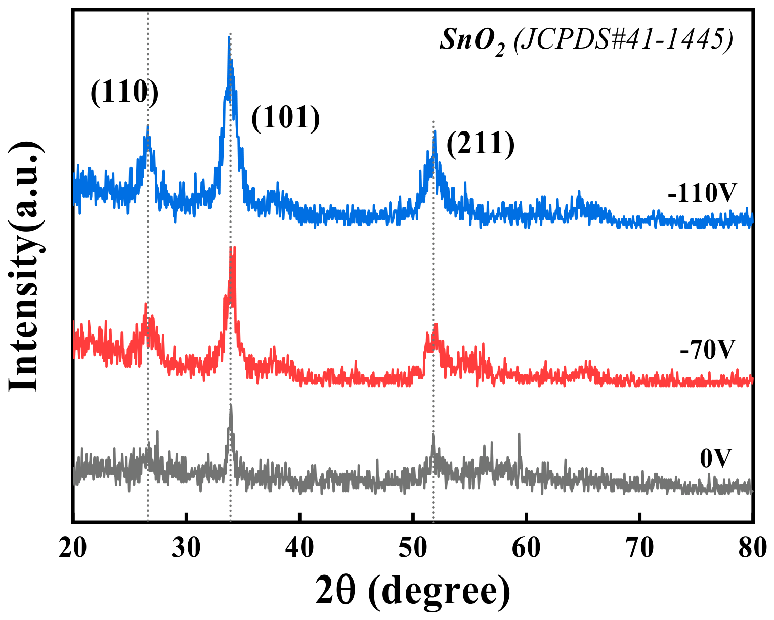
Figure 2 shows the GIXRD patterns of SnO2 films deposited under different substrate-bias conditions. All three samples exhibit the (110), (101), and (211) diffraction peaks of tetragonal rutile SnO2 (JCPDS 41-1445), located at approximately 26.6°, 33.9°, and 51.8°, respectively. As the magnitude of the negative bias increases, the intensity of the diffraction peaks becomes stronger, with the most pronounced change occurring for the (101) peak. This observation indicates that the additional ion energy introduced by the bias enhances adatom migration on the surface and facilitates lattice ordering. The film deposited at −110 V displays stronger diffraction features and indicates a further increase in crystalline order, consistent with previous results for bias-deposited SnO2 films [20]. Improved crystallinity is usually accompanied by grain growth and the possible enhanced grain-boundary effect. The former is beneficial to electron transport, while the latter usually results in grain boundary scattering and electron trapping, Consequently, the total effects on the electron transport behaviors and TFT performances were decided by the competitive interactions between the two factors.
Figure 2.
GIXRD patterns of SnO2 films deposited under different substrate-bias.
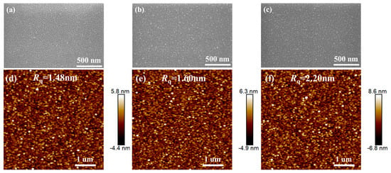
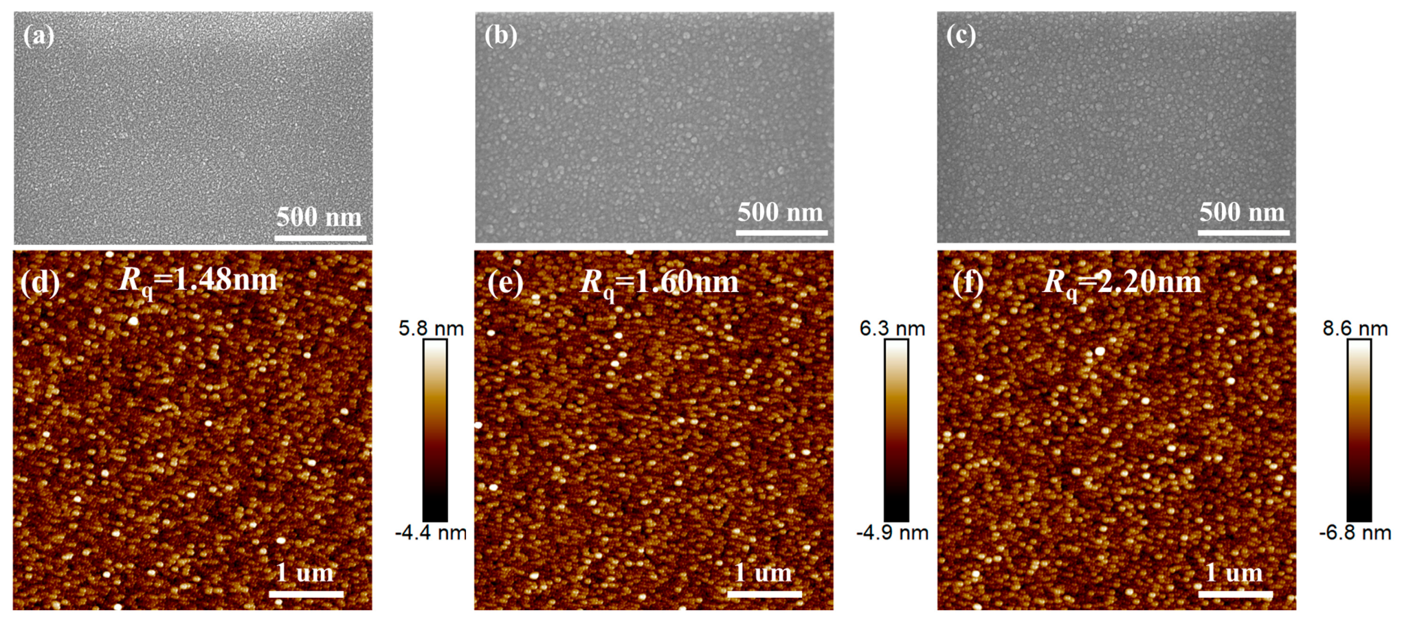
Bias-induced crystalline ordering may be accompanied by changes in film-growth morphology. SEM and AFM measurements were subsequently performed to determine whether the structural improvement was achieved at the expense of surface smoothness. The corresponding surface morphologies are compared in Figure 3. Without an applied bias, the film surface consists of fine features and is relatively smooth. At −70 V and −110 V, the films become denser and the grain size increases with a more distinct grain boundary. The root-mean-square roughness (Rq) values obtained from AFM are 1.48 nm, 1.60 nm and 2.20 nm, respectively, with increasing negative-bias magnitude. Therefore, although the bias promotes crystallization, it can also progressively roughen the surface, similar to the behavior reported for bias-deposited TiO2 films [15]. Because the interface between SnO2 and SiO2 directly participates in channel-carrier transport, the increased roughness indicates bias-induced morphological evolution of the SnO2 film, which may contribute to enhanced carrier scattering and charge trapping near the channel interface [22,23].
Figure 3.
SEM (a–c) and AFM (d–f) morphologies of SnO2 films deposited under 0 V, −70 V, and −110 V, respectively.
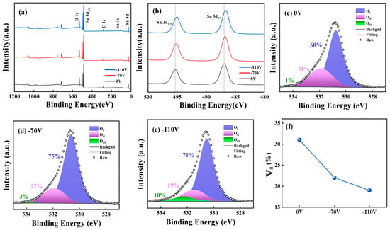
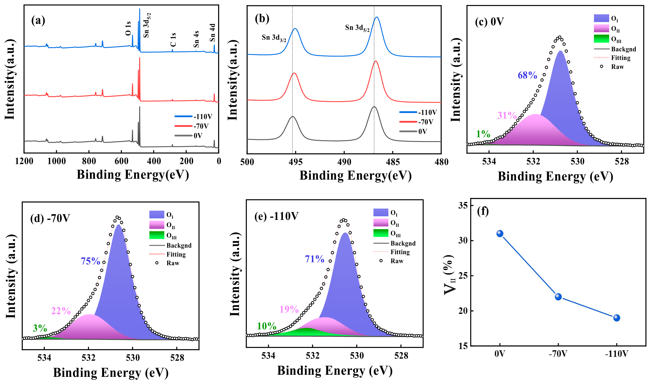
To determine how the changes in substrate bias influence the local chemical environment and oxygen-related defect states, the films were further examined by XPS. Figure 4 presents the XPS survey spectra, Sn 3d spectra, O 1s peak-fitting results, and oxygen-deficiency-related component of the SnO2 films. Only Sn, O and adventitious surface C are detected in the survey spectra. The binding energies were calibrated using the adventitious C 1s peak at 284.8 eV. The O 1s peaks can be deconvoluted into lattice oxygen (~530.7 eV), an oxygen-deficiency-related component (~531.9 eV), and adsorbed oxygen (~533.9 eV), respectively [24]. As the bias changes from 0 V to −70 V and −110 V, the relative peak-area fractions of the defect-related component decreases from 31% to 22% and then 19%, respectively, which are comparable to the references [25,26]. In SnO2 thin films, oxygen vacancies (VO) are typical donor-type defects whose formation can release electrons and affect the local oxidation state of Sn. Therefore, a decrease in oxygen vacancies is generally accompanied by an increase in the Sn oxidation state, which would theoretically shift the Sn 3d peaks toward higher binding energies. However, in this study, as the negative substrate bias increased, the oxygen-vacancy-related component in the O 1s spectra decreased, whereas the Sn 3d peaks exhibited a slight shift toward lower binding energies, suggesting that the peak shift cannot be explained solely by changes in the Sn oxidation state. Szuber et al. conducted an XPS study of L-CVD-deposited SnO2 thin films and found that, despite the reduction in oxygen vacancies after O2 treatment, the Sn 3d5/2 peak shifted by approximately 0.5 eV toward lower binding energy, which was attributed to surface band bending induced by changes in the Fermi level. In contrast, H2 treatment caused a similar shift of approximately 0.5 eV toward lower binding energy, but this shift was associated with the chemical shift induced by the reduction of Sn4+ to Sn2+, accompanied by a pronounced decrease in the O/Sn ratio [27]. Based on these findings, the low-binding-energy shift of the Sn 3d peak observed in this study may be related to bias-induced changes in surface states and band bending, while variations in film microstructure and stress state may also contribute synergistically.
Figure 4.
(a) XPS survey spectra, (b) Sn 3d spectra, (c–e) O 1s spectra, and (f) relative area fraction of the defect-related O 1s component of SnO2 films deposited under different substrate bias conditions.
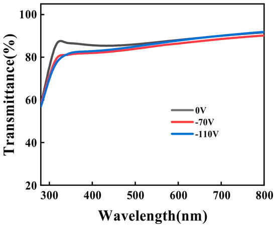
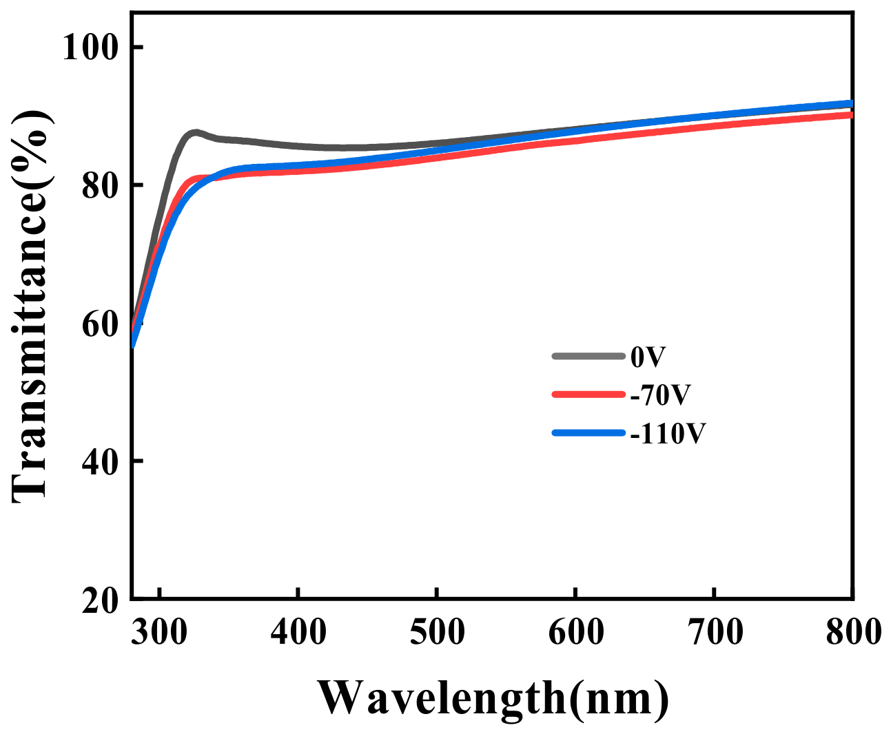
The optical transmittance was examined in the range of 300 nm–800 nm, and the spectra are presented in Figure 5. All films exhibit high transparency of approximately 80–90% in the visible region. The sharp decrease in transmittance in the ultraviolet region is attributed to the intrinsic absorption near the optical band edge of SnO2 [28,29]. Compared with the unbiased film, the films deposited at −70 V and −110 V show slightly lower transmittance in the near-UV region, while only minor differences are observed in the visible range. This variation may be associated with bias-induced ion bombardment, which modifies the crystallinity, stoichiometry, and defect states of the SnO2 films [30,31]. The similar spectra obtained at −70 V and −110 V indicate that further increasing the negative bias has only a limited effect on the optical transparency.
Figure 5.
Optical transmittance spectra of SnO2 films deposited under different substrate-bias voltages.
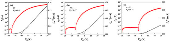
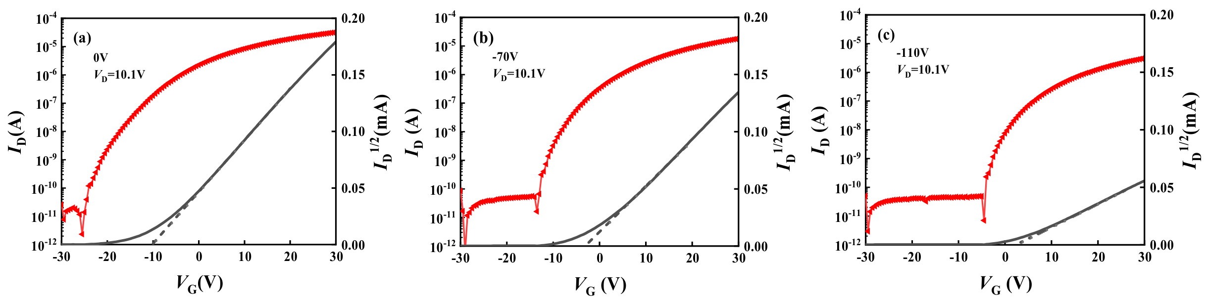
Figure 6a–c shows the transfer characteristics and the threshold voltage (Vth) of SnO2 TFTs fabricated under different substrate-bias conditions. All devices exhibit n-type switching behavior. The Vth is determined by the linear extrapolation method. As the bias changes from 0 V to −110 V, the Vth shifts positively from −10.0 to 2.3 V, consistent with the decreased content of oxygen vacancy. Because oxygen vacancies and other oxygen-related defects can influence the electron concentration in SnO2, their reduction could decrease the effective electron concentration in the channel and thereby promote a positive shift in Vth. A positive Vth achieved in −110 V bias is favorable for reducing static power consumption.
Figure 6.
Transfer characteristics of SnO2 TFTs fabricated under different substrate-bias voltages. (a) 0V, (b) -70V, (c) -110V. The red and black curves correspond to ID-VG and ID1/2-VG, respectively.
For further comparison, several key electrical parameters, including threshold voltage, subthreshold swing (SS), current on/off ratio, and field-effect mobility, were calculated using the following equations [32].
where W and L denote the channel width and length, respectively, and both of them are 500 μm. ID, VD, and VG are the drain current, drain voltage, and gate voltage, respectively. Cox is the gate-dielectric capacitance per unit area and it is 34.5 nF/cm2 for 100 nm SiO2 in this work. In the linear region (), the drain current can be expressed by Equation (1), and then the linear mobility (μlin) can be extracted. In the saturation region (), the drain current can be represented by Equation (2), and then the saturation mobility (μsat) can be calculated. In this work, VD = 0.1 V and VD = 10.1 V were adopted to calculate the μlin and μsat, respectively, and the specific values are determined by the maximum in corresponding regions. The SS can be confirmed by Equation (3). The extracted electrical parameters are summarized in Table 1. Although the 0 V device exhibits the highest linear mobility, it also has a more negative Vth and a larger SS. A substrate bias of −110 V results in a low mobility and a positive Vth. By comparison, the −70 V device retains relatively high mobility while exhibiting a Vth closer to 0 V and a lower SS, providing a best overall performance. The discrepancy between linear and saturation mobilities may mainly arise from the combined effects of gate-bias-dependent trap-state dynamics and contact resistance, as discussed in our latest publication [33]. Additionally, with the increase in negative substrate bias, the declined mobility is likely caused by the competing effects of energetic-particle bombardment during biased sputtering. Although negative substrate bias promotes film densification and crystallization, excessive bombardment can increase surface roughness and structural disorder, thereby introducing additional scattering and trapping sites [34,35]. Moreover, the reduced concentration of oxygen-deficient donor-like states may lower the free-electron concentration. Consequently, the benefits of improved crystallinity and reduced oxygen-deficient are offset by enhanced scattering, interfacial trapping, and reduced carrier availability, resulting in the decreased mobility.
Table 1.
Key electrical parameters of SnO2 TFTs fabricated under different substrate-bias voltages.
The comparisons in Table 2 show that our devices do not achieve the highest reported mobility. Nevertheless, within the present fabrication process, the −70 V condition provides a compromise among mobility, threshold voltage, subthreshold swing, and PBS stability, rather than an improvement in every performance metric, highlighting the benefits and trade-offs of substrate-bias regulation. The core contribution of this work is to identify the competing effects of substrate bias on SnO2 film properties and TFT characteristics under otherwise fixed processing conditions.
Table 2.
Performance comparisons between this work and reported literature *.
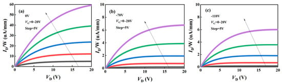
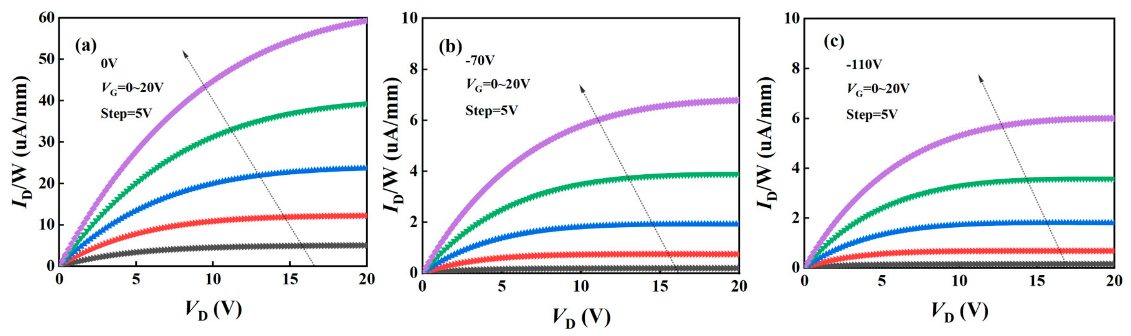
Figure 7a–c present the output characteristics of devices fabricated under different bias conditions. The drain current was converted in current density by normalizing the channel width (ID/W). The curves are nearly linear in the low-drain-voltage region and show no obvious current crowding, indicating acceptable ohmic contact between the Al electrodes and the SnO2 channels. The differences in device mobility therefore arise primarily from the channel and interface rather than from severe contact limitations, although the effects of contact resistance cannot be completely excluded due to the absence of quantitative analysis. The smaller drain current density at a larger negative substrate-bias magnitude is consistent with both the reduced mobility and the positive shift in threshold voltage. At the same applied gate voltage, a more positive threshold voltage reduces the gate overdrive and consequently the drain current. The decrease in mobility may additionally reflect the degeneration of electron transport and the declined drain current.
Figure 7.
Output characteristics of SnO2 TFTs fabricated under different substrate-bias voltages. (a) 0V, (b) -70V, (c) -110V.
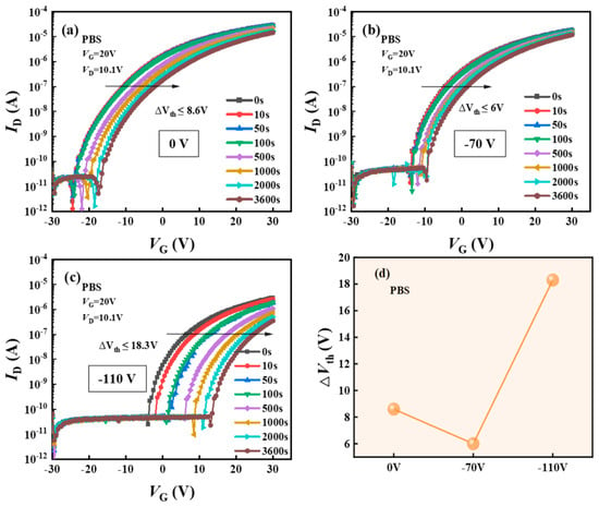
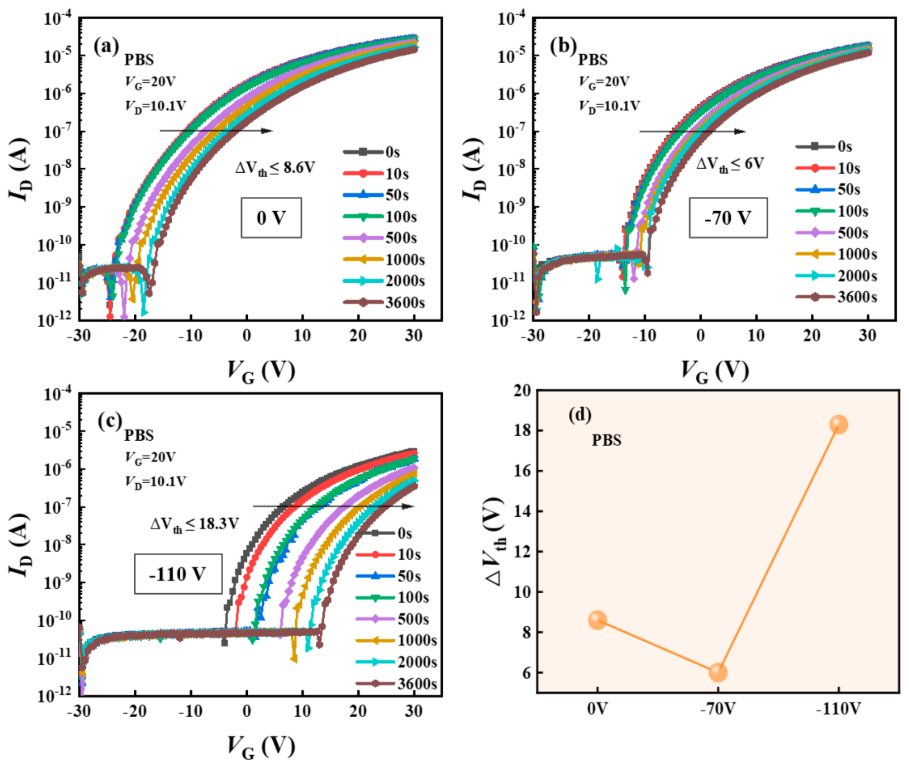
Except for the static electrical characteristics, the operational stability of the SnO2 TFTs fabricated under different substrate-bias conditions were further evaluated under prolonged electrical stress, as shown in Figure 8a–d. Under the PBS condition of VG = 20 V and VD = 10.1 V for 3600 s, the threshold voltages of the 0 V, −70 V, and −110 V devices shift positively by 8.6 V, 6.0 V, and 18.3 V, respectively. The −70 V device exhibits the best stability, whereas the −110 V device shows the largest shift despite having the smallest defect-related O 1s area fraction and the highest crystallinity. The −70 V sample has relatively low surface roughness and exhibits a smaller threshold-voltage shift. In contrast, the −110 V sample has a further-increased surface roughness and a more pronounced positive threshold-voltage shift. The PBS instability of oxide TFTs commonly originates from electron-trapping at the gate-insulator/channel interface and within the channel, where trapping states may arise from oxygen-related defects and structural disorder [43]. Positive gate bias drives electrons into these states, producing trapped negative charge that screens the gate field and causes a positive Vth shift. In this work, the PBS instability likely reflects competing effects of substrate bias on film quality and charge trapping. Although negative bias improves film crystallinity and reduces the relative area of the defect-related O 1s component, stronger ion bombardment also degrades the surface morphology and may further introduce additional structural defects [35]. The device prepared at −70 V exhibits a relatively small Vth shift, suggesting a favorable balance between these effects. At stronger bias, the increased roughness and bombardment-induced structural disorder may offset the beneficial changes in film quality. On the other hand, SnO2 is intrinsically susceptible to non-stoichiometry and oxygen-related defect states [38], which may contribute to charge trapping in the channel and near the SnO2/SiO2 interface. Therefore, the overall larger Vth shift can be attributed to the combined effects of the intrinsic defect-state background of SnO2 and bias-induced interfacial disorder.
Figure 8.
PBS stability of SnO2 TFTs fabricated under substrate-bias of (a) 0 V, (b) −70 V and (c) −110 V, as well as (d) the summarized results.
Low-frequency noise (LFN) provides complementary information on electrically active defects and carrier-transport fluctuations. In Si-doped IZO TFT-type gas sensors, suppressing oxygen-vacancy-related subgap states reduces 1/f noise and improves thermal stability [44]. Studies on CMOS-integrated gas sensors further demonstrate the relevance of LFN to device reliability and defect-related processes [45]. In ALD IGZO TFTs, the dominant noise mechanism shifted from mobility fluctuations toward carrier-number fluctuations as the channel length decreased, highlighting the dependence of noise origins on device dimensions [46]. Furthermore, LFN-based analysis revealed spatially localized gate-insulator degradation near the drain in self-aligned top-gate IGZO TFTs after saturation stress [47]. These findings indicate that the substrate-bias-induced changes in defect-related states and transport in our SnO2 TFTs warrant complementary LFN characterization. However, neither the reduced defect-related O 1s area fraction nor the smaller PBS-induced threshold-voltage shift at −70 V necessarily implies lower noise, and the present measurements cannot distinguish carrier-number fluctuations from mobility fluctuations or locate the electrically active traps. Therefore, charge trapping in the channel/interface region remains a plausible explanation for the PBS behavior, while the specific contribution to LFN requires further verification.
Taken together, the structural, chemical, morphological, and electrical results indicate that substrate bias does not affect the SnO2 TFTs through a single mechanism. Instead, the improvement in bulk film ordering competes with bias-induced changes in growth morphology and interfacial transport, giving rise to the distinct device behavior observed under the three deposition conditions. A competition model for substrate-bias regulation can therefore be established. Increasing bias improves crystallinity, reduces oxygen vacancies, and shifts Vth positively, but it also increases surface roughness, may strengthen interface scattering and trapping, decreases mobility, and degrades stability. The −70 V condition lies in the balance region between these effects, whereas −110 V could enter an interface-damage-dominated regime [15,48].
4. Conclusions
This study investigated the effects of substrate biases of 0 V, −70 V, and −110 V on the structure of radio-frequency magnetron-sputtered SnO2 films and the transistor performances. As the magnitude of the negative bias increased, the film crystallinity became more pronounced, and the relative area fraction of the defect-related O 1s component decreased from 31% to 19%, accompanied by the roughness increasing from 1.48 nm to 2.20 nm. In addition, the increased negative bias shifted the Vth from −10.0 V to 2.3 V, while the linear mobility decreased from 4.2 cm2/Vs to 0.6 cm2/Vs. The device fabricated at −70 V retained a relatively high linear mobility of 3.7 cm2/Vs while exhibiting a low SS of 0.61 V/dec and a smaller threshold-voltage shift of 6.0 V after 3600 s under the PBS condition. Further analyses indicate that the device performance is not only determined by the bulk crystal structure and oxygen-related defects but also competition with bias-induced changes in growth morphology and interfacial transport. The findings provide new insight into the competing effects of substrate-bias-induced structural, defect-related, and interfacial modifications on electron transport in oxide semiconductors.
Author Contributions
Z.H.: investigation, writing—original draft. W.P. (Wenwu Pan): validation, writing—review and editing. K.G.: resources, data curation. S.W.: formal analysis, software. P.G.: conceptualization. H.J.: methodology. Y.L.: visualization, supervision. W.P. (Wengao Pan): funding acquisition, project administration. All authors have read and agreed to the published version of the manuscript.
Funding
This work was financially supported by High-level Talent Research Start-up Project Funding of Henan Academy of Sciences (231817004, 231817066), the Fundamental Research Fund of Henan Academy of Sciences (240617060), Joint Fund of Henan Province Science and Technology R&D Program (235200810090), the Scientific and Technological Research Project of Henan Academy of Sciences (20252317005, 20262317009), and Shenzhen Polytechnic High-level Talent Start-up Project Funds (6023330006K). Ziyue Hu and Wenwu Pan contributed equally to this work.
Institutional Review Board Statement
Not applicable.
Informed Consent Statement
Not applicable.
Data Availability Statement
The original contributions presented in this study are included in the article material. Further inquiries can be directed to the corresponding authors.
Conflicts of Interest
Wenwu Pan is an employee of Crane Semicon Technology Co., Ltd., Shanghai, China.
References
- Nomura, K.; Ohta, H.; Takagi, A.; Kamiya, T.; Hirano, M.; Hosono, H. Room-temperature fabrication of transparent flexible thin-film transistors using amorphous oxide semiconductors. Nature 2004, 432, 488–492. [Google Scholar] [CrossRef] [Scilit]
- Kamiya, T.; Hosono, H. Material characteristics and applications of transparent amorphous oxide semiconductors. NPG Asia Mater. 2010, 2, 15–22. [Google Scholar] [CrossRef] [Scilit]
- Fortunato, E.; Barquinha, P.; Martins, R. Oxide semiconductor thin-film transistors: A review of recent advances. Adv. Mater. 2012, 24, 2945–2986. [Google Scholar] [CrossRef] [Scilit]
- Chang, H.; Huang, C.-H.; Nomura, K. Low-temperature solution-processed n-channel SnO2 thin-film transistors and high-gain zero-VGS-load inverter. ACS Appl. Electron. Mater. 2021, 3, 4943–4949. [Google Scholar] [CrossRef] [Scilit]
- Liang, D.; Chen, B.-J.; Feng, B.; Ikuhara, Y.; Cho, H.J.; Ohta, H. Optimization of two-dimensional channel thickness in nanometer-thick SnO2-based top-gated thin-film transistors using electric field thermopower modulation: Implications for flat-panel displays. ACS Appl. Nano Mater. 2020, 3, 12427–12432. [Google Scholar] [CrossRef] [Scilit]
- Mai, L.; Zanders, D.; Subaşı, E.; Ciftyurek, E.; Hoppe, C.; Rogalla, D.; Gilbert, W.; de los Arcos, T.; Schierbaum, K.; Grundmeier, G.; et al. Low-temperature plasma-enhanced atomic layer deposition of tin(IV) oxide from a functionalized alkyl precursor: Fabrication and evaluation of SnO2-based thin-film transistor devices. ACS Appl. Mater. Interfaces 2019, 11, 3169–3180. [Google Scholar] [CrossRef] [Scilit]
- Jang, B.; Kim, J.; Lee, J.; Park, G.; Yang, G.; Jang, J.; Kwon, H.-J. Combustion-assisted low-temperature ZrO2/SnO2 films for high-performance flexible thin film transistors. npj Flex. Electron. 2024, 8, 74. [Google Scholar] [CrossRef] [Scilit]
- Tang, X.; Luo, F.; Ou, F.; Zhou, W.; Zhu, D.; Huang, Z. Effects of negative substrate bias voltage on the structure and properties of aluminum oxide films prepared by DC reactive magnetron sputtering. Appl. Surf. Sci. 2012, 259, 448–453. [Google Scholar] [CrossRef] [Scilit]
- Zhou, G.; Wang, L.; Wang, X.; Yu, Y.; Mutzke, A. Effect of bias voltage on microstructure and optical properties of Al2O3 thin films prepared by twin targets reactive high power impulse magnetron sputtering. Vacuum 2019, 166, 88–96. [Google Scholar] [CrossRef] [Scilit]
- Ma, H.-L.; Hao, X.-T.; Ma, J.; Yang, Y.-G.; Huang, S.-L.; Chen, F.; Wang, Q.; Zhang, D.-H. Bias voltage dependence of properties for ZnO:Al films deposited on flexible substrate. Surf. Coat. Technol. 2002, 161, 58–61. [Google Scholar] [CrossRef] [Scilit]
- Lee, J.H.; Song, J.T. Dependence of the electrical and optical properties on the bias voltage for ZnO:Al films deposited by r.f. magnetron sputtering. Thin Solid Films 2008, 516, 1377–1381. [Google Scholar] [CrossRef] [Scilit]
- Castro, M.V.; Tavares, C.J. Dependence of Ga-doped ZnO thin film properties on different sputtering process parameters: Substrate temperature, sputtering pressure and bias voltage. Thin Solid Films 2015, 586, 13–21. [Google Scholar] [CrossRef] [Scilit]
- Sujatha, C.; Rao, G.M.; Uthanna, S. Characteristics of indium tin oxide films deposited by bias magnetron sputtering. Mater. Sci. Eng. B 2002, 94, 106–110. [Google Scholar] [CrossRef] [Scilit]
- Chandra Sekhar, M.; Kondaiah, P.; Jagadeesh Chandra, S.V.; Mohan Rao, G.; Uthanna, S. Effect of substrate bias voltage on the structure, electric and dielectric properties of TiO2 thin films by DC magnetron sputtering. Appl. Surf. Sci. 2011, 258, 1789–1796. [Google Scholar] [CrossRef] [Scilit]
- Nezar, S.; Saoula, N.; Sali, S.; Faiz, M.; Mekki, M.; Laoufi, N.A.; Tabet, N. Properties of TiO2 thin films deposited by rf reactive magnetron sputtering on biased substrates. Appl. Surf. Sci. 2017, 395, 172–179. [Google Scholar] [CrossRef] [Scilit]
- Liang, L.Y.; Cao, H.T.; Liu, Q.; Jiang, K.M.; Liu, Z.M.; Zhuge, F.; Deng, F.L. Substrate biasing effect on the physical properties of reactive RF-magnetron-sputtered aluminum oxide dielectric films on ITO glasses. ACS Appl. Mater. Interfaces 2014, 6, 2255–2261. [Google Scholar] [CrossRef] [Scilit]
- Xi, Y.; Qin, X.; Li, W.; Luo, X.; Zhang, J.; Liu, W.; Yang, P. Effect of substrate negative bias on the microstructural, optical, mechanical, and laser damage resistance properties of HfO2 thin films grown by DC reactive magnetron sputtering. Micromachines 2023, 14, 1800. [Google Scholar] [CrossRef] [Scilit]
- Reddy, A.M.; Reddy, A.S.; Reddy, P.S. Effect of substrate bias voltage on the physical properties of dc reactive magnetron sputtered NiO thin films. Mater. Chem. Phys. 2011, 125, 434–439. [Google Scholar] [CrossRef] [Scilit]
- Mei, H.; Wang, W.; Zhao, J.; Zhong, W.; Qiu, M.; Xu, J.; Gao, K.; Liu, G.; Liang, J.; Gong, W. Effect of bias voltage on the microstructure and photoelectric properties of W-doped ZnO films. Nanomaterials 2024, 14, 2050. [Google Scholar] [CrossRef] [Scilit]
- Prathyusha, T.; Srikanth, T.; Sivasankar Reddy, A.; Sreedhara Reddy, P.; Seshendra Reddy, C. Effect of substrate bias voltage and substrate temperature on the physical properties of dc magnetron sputtered SnO2 thin films. Optik 2016, 127, 9457–9463. [Google Scholar] [CrossRef] [Scilit]
- Zhang, M.; Xiao, X.; Ju, X.; Zhang, X.; Zhang, S. Characteristics of amorphous In-Ga-Zn-O thin-film-transistors with channel layer deposited by bias sputtering. In Proceedings of the 2016 23rd International Workshop on Active-Matrix Flatpanel Displays and Devices (AM-FPD), Kyoto, Japan, 6–8 July 2016; pp. 127–130. [Google Scholar]
- Li, J.; Ju, S.; Tang, Y.; Li, J.; Li, X.; Tian, X.; Zhu, J.; Ge, Q.; Lu, L.; Zhang, S.; et al. Remarkable bias-stress stability of ultrathin atomic-layer-deposited indium oxide thin-film transistors enabled by plasma fluorination. Adv. Funct. Mater. 2024, 34, 2401170. [Google Scholar] [CrossRef] [Scilit]
- Wang, X.; Dodabalapur, A. Interface roughness and interface roughness scattering in amorphous oxide thin-film transistors. J. Appl. Phys. 2021, 130, 145302. [Google Scholar] [CrossRef] [Scilit]
- Nascimento, E.P.; Araujo, R.N.; Firmino, H.C.T.; Mastelaro, V.R.; Loureiro, F.J.A.; Neves, G.A.; Medeiros, E.S.; Menezes, R.R. Parallel-solution blow spun Al-SnO2/F-SnO2 fibers as an efficient room temperature ethanol sensor. Ceram. Int. 2022, 48, 13163–13174. [Google Scholar] [CrossRef] [Scilit]
- Kumar, V.; Kumar, V.; Som, S.; Neethling, J.H.; Lee, M.; Ntwaeaborwa, O.M.; Swart, H.C. The role of surface and deep-level defects on the emission of tin oxide quantum dots. Nanotechnology 2014, 25, 135701. [Google Scholar] [CrossRef] [Scilit]
- Liang, Y.C.; Lee, C.M.; Lo, Y.J. Reducing gas-sensing performance of Ce-doped SnO2 thin films through a cosputtering method. RSC Adv. 2017, 7, 4724–4734. [Google Scholar] [CrossRef] [Scilit]
- Szuber, J.; Czempik, G.; Larciprete, R.; Koziej, D.; Adamowicz, B. XPS study of the L-CVD deposited SnO2 thin films exposed to oxygen and hydrogen. Thin Solid Films 2001, 391, 198–203. [Google Scholar] [CrossRef] [Scilit]
- Summitt, R.; Marley, J.A.; Borrelli, N.F. The ultraviolet absorption edge of stannic oxide (SnO2). J. Phys. Chem. Solids 1964, 25, 1465–1469. [Google Scholar] [CrossRef] [Scilit]
- Shanthi, E.; Dutta, V.; Banerjee, A.; Chopra, K.L. Electrical and optical properties of undoped and antimony-doped tin oxide films. J. Appl. Phys. 1980, 51, 6243–6251. [Google Scholar] [CrossRef] [Scilit]
- Tao, Y.; Zhu, B.; Yang, Y.; Wu, J.; Shi, X. The structural, electrical, and optical properties of SnO2 films prepared by reactive magnetron sputtering: Influence of substrate temperature and O2 flow rate. Mater. Chem. Phys. 2020, 250, 123129. [Google Scholar] [CrossRef] [Scilit]
- Saipriya, S.; Sultan, M.; Singh, R. Effect of environment and heat treatment on the optical properties of RF-sputtered SnO2 thin films. Physica B 2011, 406, 812–817. [Google Scholar] [CrossRef] [Scilit]
- Pan, W.; Zhou, X.; Lin, Q.; Chen, J.; Lu, L.; Zhang, S. Low temperature and high-performance ZnSnO thin-film transistors engineered by in situ thermal manipulation. J. Mater. Chem. C 2022, 10, 3129–3138. [Google Scholar] [CrossRef] [Scilit]
- Guo, P.; Pan, W.; Gu, K.; Hu, Z.; Wei, S.; Tian, Y.; Jing, H.; Wu, X.; Li, Y.; Pan, W. Enhanced performance of In2O3/SnO2 dual-channel thin-film transistor by heterostructure strategy. Materials 2026, 19, 4284. [Google Scholar] [CrossRef] [Scilit]
- Nulhakim, L.; Makino, H. Change of scattering mechanism and annealing out of defects on Ga-doped ZnO films deposited by radio-frequency magnetron sputtering. J. Appl. Phys. 2016, 119, 235302. [Google Scholar] [CrossRef] [Scilit]
- Correia, F.C.; Bundaleski, N.; Teodoro, O.M.N.D.; Correia, M.R.; Rebouta, L.; Mendes, A.; Tavares, C.J. XPS analysis of ZnO:Ga films deposited by magnetron sputtering: Substrate bias effect. Appl. Surf. Sci. 2018, 458, 1043–1049. [Google Scholar] [CrossRef] [Scilit]
- Lee, W.-Y.; Kim, D.W.; Kim, H.J.; Kim, K.; Lee, S.-H.; Bae, J.-H.; Kang, I.-M.; Kim, K.; Jang, J. Environmentally and electrically stable sol–gel-deposited SnO2 thin-film transistors with controlled passivation layer diffusion penetration depth that minimizes mobility degradation. ACS Appl. Mater. Interfaces 2022, 14, 10558–10565. [Google Scholar] [CrossRef] [Scilit]
- Park, H.; Choi, H.; Lee, N.; Jung, C.; Choi, Y.; Song, S.; Choi, Y.; Kim, K.; Kim, J.; Lee, J.; et al. Effect of single Al2O3 cycle insertion with various positions in SnO2 thin films using atomic layer deposition. Ceram. Int. 2020, 46, 12782–12787. [Google Scholar] [CrossRef] [Scilit]
- Gu, K.; Zhao, K.; Xu, L.; Xiao, L.; Cao, S.; Feng, S.; Jing, H.; Zhu, Z.; Li, Y.; Yang, W.; et al. Enhanced performances of SnO2 thin film transistor by nitrogen modification for low-cost display application. Mater. Sci. Eng. B 2026, 323, 118873. [Google Scholar] [CrossRef] [Scilit]
- Liang, D.-D.; Chen, B.; Cho, H.J.; Ohta, H. Thickness optimization toward high-performance bottom-gated transparent tin dioxide thin-film transistors. ACS Appl. Electron. Mater. 2020, 2, 3454–3458. [Google Scholar] [CrossRef] [Scilit]
- Lee, B.K.; Jung, E.; Kim, S.H.; Moon, D.C.; Lee, S.S.; Park, B.K.; Hwang, J.H.; Chung, T.-M.; Kim, C.G.; An, K.-S. Physical/chemical properties of tin oxide thin film transistors prepared using plasma-enhanced atomic layer deposition. Mater. Res. Bull. 2012, 47, 3052–3055. [Google Scholar] [CrossRef] [Scilit]
- Lim, D.; Jeon, Y.; Kim, M.; Kim, Y.; Kim, S. Electrical characteristics of SnO2 thin-film transistors fabricated on bendable substrates using reactive magnetron sputtering. J. Nanosci. Nanotechnol. 2016, 16, 11697–11700. [Google Scholar] [CrossRef] [Scilit]
- Kim, D.W.; Kim, H.J.; Lee, C.; Kim, K.; Bae, J.-H.; Kang, I.-M.; Jang, J. Influence of active channel layer thickness on SnO2 thin-film transistor performance. Electronics 2021, 10, 200. [Google Scholar] [CrossRef] [Scilit]
- Lee, J.-M.; Cho, I.-T.; Lee, J.-H.; Kwon, H.-I. Bias-stress-induced stretched-exponential time dependence of threshold voltage shift in InGaZnO thin film transistors. Appl. Phys. Lett. 2008, 93, 093504. [Google Scholar] [CrossRef] [Scilit]
- Shin, W.; Lee, S.; Koo, R.-H.; Kim, J.; Lee, S.Y.; Lee, S.-T. Does a large response suffice?: Thermally stable and low noise Si-doped IZO thin-film transistor-type gas sensors. Sens. Actuators B Chem. 2025, 422, 136498. [Google Scholar] [CrossRef] [Scilit]
- Lee, C.; Jeong, Y.; Koo, R.-H.; Cho, Y.; Choi, K.; Jung, G.; Kim, J.; Hong, S.; Im, J.; Lee, S.-T.; et al. Low-frequency noise in CMOS-integrated gas sensors: From a reliability constraint to a selective sensing feature. Sens. Actuators B Chem. 2026, 446, 138701. [Google Scholar] [CrossRef] [Scilit]
- Lee, S.; Niu, C.; Shih, C.-A.; Lin, J.-Y.; Zhang, Z.; Zhang, Y.; Long, L.; Wang, H.; Alam, M.A.; Ye, P.D. Comprehensive study of low-frequency noise origins in scaled atomic-layer-deposited IGZO TFTs. IEEE Trans. Electron Devices 2025, 72, 2993–2999. [Google Scholar] [CrossRef] [Scilit]
- Lee, D.-H.; Hwang, J.-H.; Oh, C.-E.; Ryu, J.; Jang, J.-M.; Ahn, B.-D.; Bae, J.-U.; Kwon, H.-I. Lateral distribution of electrical defect concentration in SA TG coplanar IGZO TFTs extracted via low frequency noise analysis. Sci. Rep. 2026, 16, 27259. [Google Scholar] [CrossRef] [Scilit]
- Lee, T.; Kim, K.; Kim, H.-I.; Lee, S.-H.; Bae, J.-H.; Kang, I.-M.; Kim, K.; Lee, W.-Y.; Jang, J. Improved negative bias stability of sol–gel-processed SnO2 thin-film transistors with vertically controlled carrier concentrations. ACS Appl. Electron. Mater. 2023, 5, 2670–2677. [Google Scholar] [CrossRef] [Scilit]

Disclaimer/Publisher’s Note: The statements, opinions and data contained in all publications are solely those of the individual author(s) and contributor(s) and not of MDPI and/or the editor(s). MDPI and/or the editor(s) disclaim responsibility for any injury to people or property resulting from any ideas, methods, instructions or products referred to in the content. |
© 2026 by the authors. Licensee MDPI, Basel, Switzerland. This article is an open access article distributed under the terms and conditions of the Creative Commons Attribution (CC BY) license.