


Abstract
In this review, low-temperature Sn-Bi and Sn-Zn solders and the reliability of their Cu interfaces are summarized for advanced electronic packaging. Sn-58Bi can markedly reduce the soldering temperature because its eutectic temperature is approximately 139 °C; however, the brittle Bi-rich phase and the coarsening of the two-phase microstructure remain important problems. The addition of Zn or In has been used to reduce these problems. Bi addition to Sn-3.5Ag and Sn-9Zn also decreased the melting temperature and increased the joint strength under selected conditions. In addition, electrodeposited Sn/Bi bilayers and Sn-Sb/Sn-Bi mixed solders provide another route to form low-temperature joints during heating. The Cu interface was also considered because Cu6Sn5/Cu3Sn morphology, impurities in electroplated Cu, Cu grain size, and surface finish strongly affect IMC growth and void formation. The effects of thermomigration and electromigration are also discussed because they become important as the joint size decreases. This review will provide useful information for understanding low-temperature solder materials and for designing reliable Cu/solder interfaces for advanced electronic packaging.
1. Introduction
With advances in high-density and heterogeneous electronic packaging, the demand for the materials of low-temperature solder is increasing [1,2,3,4]. Sn-Ag-Cu (SAC) alloys are widely used as Pb-free solders because of their good joining strength and mechanical reliability. However, the melting temperature of SAC solders is approximately 217–220 °C, and the assembly process of the chips requires a reflow step at a peak temperature near 250 °C [5,6]. The high reflow temperature can cause problems in large and thin packages due to the different thermal coefficients among Si chips, organic substrates, and printed circuit boards (PCBs). The thermal mismatch of different materials can increase the warpage of package during reflow [5]. Therefore, a soldering process at a lower temperature is needed to reduce the thermal loading of advanced packages.
Sn-58Bi is one of the most widely studied low-temperature solders because its eutectic temperature is approximately 139 °C [2,4]. The low melting temperature can greatly decrease the reflow temperature compared with SAC solder; however, the Sn-58Bi alloy consists of Sn-rich and Bi-rich phases and the brittle Bi-rich phase limits the ductility. Thermal aging also causes coarsening of the two-phase microstructure. Raeder et al. reported the coarsening and the change in fracture behavior after aging Sn-Bi/Cu joints at 80 °C. To reduce these problems, small amounts of In, Zn, and other alloying elements have been added to Sn-Bi solders [7,8,9,10,11,12]. In addition, Shang et al. showed that the reaction at the Cu interface was related to the change in the Bi phase inside the solder [13]. This suggests that the bulk Sn-Bi microstructure changes together with the interfacial reaction during aging.
Sn-Zn is another example for Pb-free solder that has a relatively low melting temperature, which is around 199 °C [14,15,16,17]. The intermediate melting temperature in the range between SAC and SnBi alloys allows a reflow process at a lower temperature than that of SAC solder while providing a wider range of service temperature than that of Sn-58Bi solder system. However, the rapid oxidation of Zn cause the degradation of wettability of the solders that limits the practical application of Sn-Zn solder to electronic packaging [15,16]. Sn-Zn solder system also shows the different reaction behavior with Cu from the Sn-based solder system, where Cu-Zn IMCs such as Cu5Zn8 can form at the interface [14,15,16,17]. For the practical use of Sn-Zn solder, therefore, the precise control of both the oxidation behavior and the interfacial reaction is required. One example is adding Bi in Sn-9Zn to lower the melting temperature and improve wettability and joint strength [14].
The Cu pad also has an important role in solder-joint reliability. Cu6Sn5 and Cu3Sn are formed at most Sn-based solder/Cu interfaces, and their growth depends on the initial IMC morphology and grain structure. For electroplated Cu, organic suppressors, accelerators, and other additives can remain in the Cu layer after electrodeposition. The incorporated impurities have been related to the formation of voids near Cu3Sn during thermal aging [18,19,20,21,22]. Furthermore, current density and temperature gradients become larger as the solder joint becomes smaller, and directional atomic migration by electromigration and thermomigration should also be considered [23,24,25,26,27,28,29].
So far, several reviews have discussed low-melting-temperature Pb-free solders, however, there are lacks of discussion about the relationships among composition of alloys, bonding methods, and interfacial degradation of Cu in Sn-Bi and Sn-Zn solder systems. In this review, the effects of alloying additions or reactive bilayers on Sn-Bi and Sn-Zn solders are discussed. Reactions at Cu/solder interface, IMC growth, Kirkendall void formation, thermomigration, and electromigration during the bonding process are discussed. In addition, Cu-Cu direct bonding is briefly discussed as an alternative interconnection system for ultra fine-pitch electronic packaging.
2. Solder Materials for Low-Temperature Bonding
Among the Pb-free solders used for low-temperature bonding, Sn-58Bi has attracted considerable attention because of its low eutectic temperature of approximately 139 °C [2,4]. Such a low melting temperature is useful especially for heat-sensitive components in electronic devices as well as for the large scale packaging process where thermal deformation during reflow can become significant. However, Sn-58Bi has two-phase microstructure of Sn-rich/Bi-rich, which cause the degradation of ductility and the thermal failure during continuous thermal exposure. For example, Raeder et al. aged Sn-Bi/Cu joints at 80 °C for 3–30 days and observed significant coarsening of the two phases [7]. Fracture behavior also varied depending on the aging condition and strain rate [7]. They stressed out that the microstructure of Sn-58Bi solder can change even at much lower aging temperature than the melting temperature of Sn-58Bi.
Alloying has therefore been widely used to improve the microstructural stability of Sn-Bi solder. Mokhtari and Nishikawa reported that it reduced Bi coarsening and excessive IMC growth while improving the ductility [8]. Zhou et al. obtained a finer Sn-rich/Bi-rich structure by adding 0.5–1 wt.% Zn to Sn-58Bi [11]. The reduced coarsening was attributed to Zn segregation at the Sn/Bi phase boundaries, which suppressed atomic diffusion. A similar approach was used by Hirata et al., who added In to Sn-45Bi-2.6Zn and discussed the combined effect of Zn segregation and In solid solution in the Sn matrix [9]. Low-Bi Sn-Bi-Zn(-In) joints also maintained their shear strength after aging at 80 °C for 1008 h [10]. The effect of Zn, however, was dependent on the solder composition and joining condition. Mokhtari et al., for example, observed reduced IMC growth but lower shear strength under some conditions [12]. Such suppression of Bi coarsening alone does not necessarily result in improved joint strength. The difference in trends may reflect competing contributions from strengthening of the Sn-rich matrix, the size and distribution of brittle Bi-rich phases, interfacial IMC morphology, and the location of fracture. Such relative importance depends on the history of composition and processing; thus, reduced phase coarsening or IMC growth does not necessarily result in higher joint strength [8,9,10,11,12].
The microstructure of Sn-Bi solder is also affected by its reaction with the Cu substrate. Shang et al. changed the soldering temperature and cooling rate and obtained different initial Cu6Sn5 and Cu3Sn structures at the Cu interface [13]. Changes in the interfacial reaction occurred together with aggregation, dissolution, separation, and coarsening of the Bi phase in the solder. Thus, the evolution of the Bi-rich phase cannot be considered independently from the reaction at the Cu interface. This becomes important when Bi is used not only as the main component of a low-temperature solder but also as an alloying element in other Sn-based solders.
Bi can be also added to Sn-Ag system to decrease the melting temperature as well as to tune the microstructure of solder system [30]. For example, Shen et al. investigated the effect of Bi addition to Sn-3.5Ag solder [30]. The DSC onset temperature decreased from 219.8 °C to 198.6 °C with the addition of 5 wt.% Bi. The strength of the solder through solid-solution and precipitation strengthening was also increased by the Bi addition. Meanwhile, the thickness of interfacial IMC also increased with Bi content that suggest that the mechanical strength of solder joints depends on both the solder matrix and the interfacial IMC.
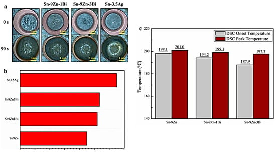
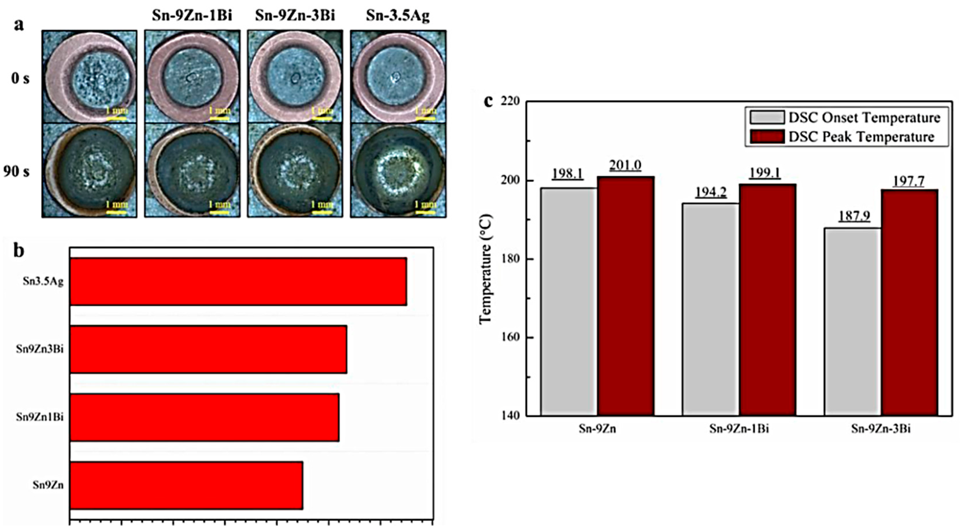
Bi addition in Sn-Zn system allows the enhancement of wettability and bonding reliability. The melting temperature can also be decreased by Bi addition [14,16,17]. Shen et al. studied the effects of adding 1 and 3 wt.% Bi to Sn-9Zn solders [14]. Figure 1 shows the effects of Bi addition on the wetting and melting behavior. Figure 1a presents optical microscope images of Sn-9Zn (SZ9), Sn-9Zn-1Bi (SZB91), Sn-9Zn-3Bi (SZB93), and Sn-3.5Ag (SA3.5) before and after reflow on Cu at 250 °C for 90 s [14]. The spreading rates increased from approximately 90% for SZ9 to 104% for SZB91 and 107% for SZB93, as shown in Figure 1b. Figure 1c shows the corresponding differential scanning calorimetry (DSC) curves. The melting onset temperature decreased from 198.1 °C for SZ9 to 194.2 °C for SZB91 and 187.9 °C for SZB93, while the peak temperature decreased slightly from 201.0 °C to 197.7 °C. These results indicate that Bi addition improves solder spreading and reduces the onset temperature of melting. EPMA analysis and thermodynamic calculations further indicated that most of the 3 wt.% Bi remained in the Sn-rich matrix with slight supersaturation [14].
Figure 1.
(a) Optical images of SZ9, SZB91, SZB93, and SA3.5 solder alloys before and after reflow on Cu substrates at 250 ◦C for 90 s. (b) Measured spreading rates of the solder alloys on Cu substrates. (c) DSC measurements of the thermal behaviors (the onset and peak temperature) of SZ9, SZB91, and SZB93 alloys. (reproduced with permission from Ref. [14]).
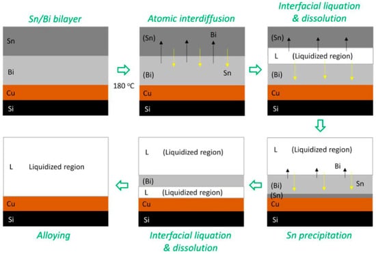
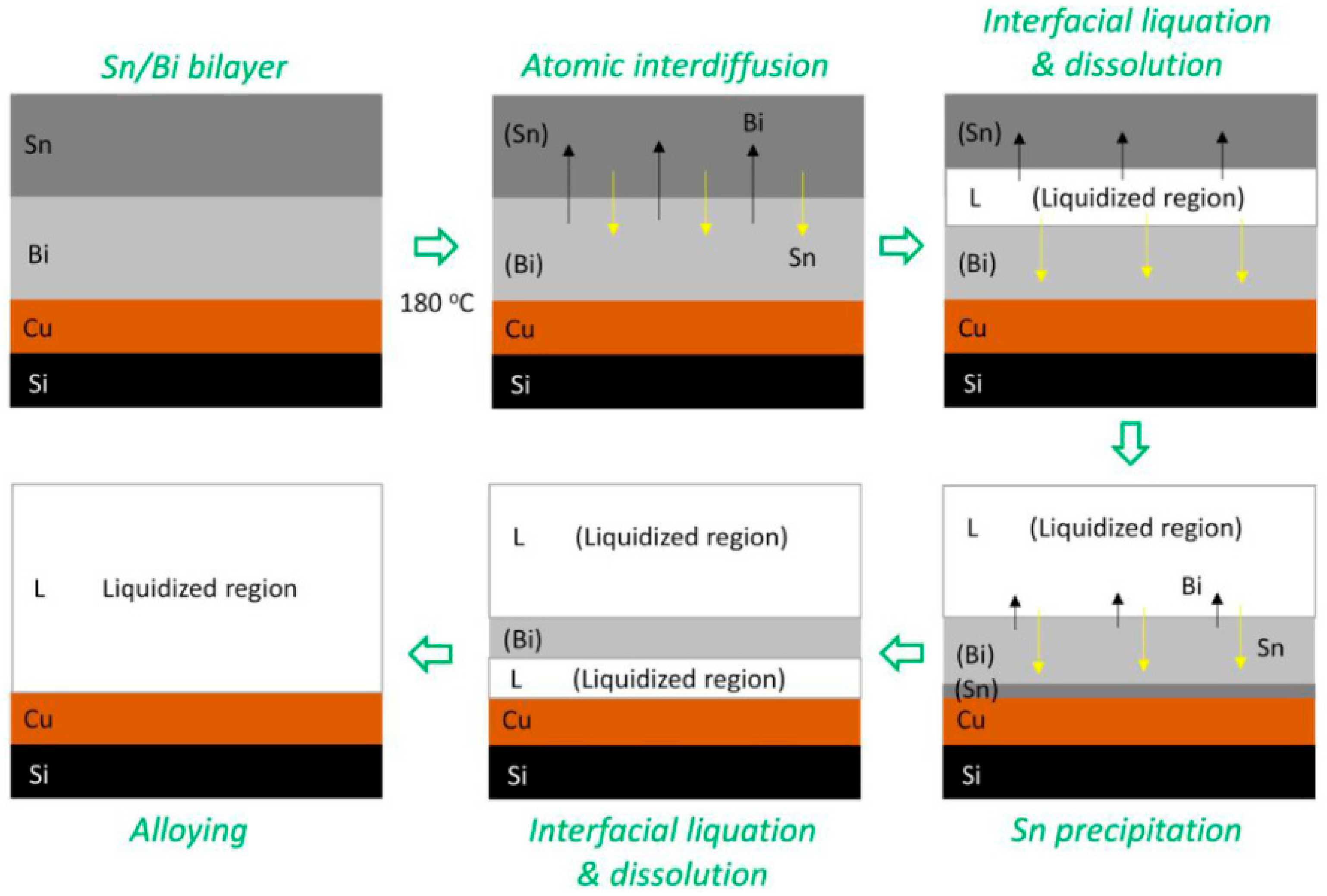
The examples discussed above are based on the modification of a solder alloy before joining. Another approach is to form the final solder composition during heating. Wang et al. used sequentially electrodeposited Sn and Bi layers because uniform co-deposition of Sn and Bi is difficult owing to their different electrochemical behavior [31]. Approximately 10-μm-thick Bi and 9-μm-thick Sn layers were deposited, giving an overall composition close to Sn-59.6 wt.% Bi. During heating at 180 °C, interfacial liquation started within 5 s, followed by the formation of a eutectic-like two-phase structure after approximately 30 s. The proposed reaction process is illustrated in Figure 2. Sn and Bi first interdiffuse at the original interface, and a liquid phase is then formed between β-Sn and Bi. Further dissolution of Sn and Bi occurs at the β-Sn/liquid and liquid/Bi interfaces. Sn precipitation near the Bi/Cu interface generates another Bi/Sn interface, where interfacial liquation occurs again. With further reaction, the band-shaped Bi layer disappears and the entire region changes to a eutectic-like (Sn) + (Bi) structure. The representative low-temperature solder and reactive-joining systems discussed above are summarized in Table 1.
Figure 2.
Illustration of the history of microstructural evolution of the Sn/Bi electrodeposited bilayer under thermal annealing at 180 °C (reproduced with permission from Ref. [31]). Arrows indicate the direction of diffusion.
Table 1.
Summary of characteristics of low-temperature solders.
3. Cu/Solder Interfaces: IMC Growth and Kirkendall Voids
3.1. Cu–Sn IMC Formation and Growth
When Sn-based solder reacts with Cu, Cu6Sn5 is generally formed first and Cu3Sn is developed during a longer reaction or solid-state aging [6,20]. The IMCs are required for metallurgical bonding; however, excessive growth of a thick and continuous IMC layer can increase brittle fracture. In addition to the IMC thickness, the initial morphology of Cu6Sn5 is also important for the subsequent reaction. Lee et al., investigated the IMC dependence on mechanical reliabilities for SAC305/Cu joints [6]. The joints were reacted at 265 °C for 1–60 min and then aged at 200 °C. A longer initial reaction produced a thicker Cu6Sn5 layer with larger grains. However, the growth rate during subsequent aging decreased, as the growth-rate constant decreased from 0.508 to 0.151 μm/h0.5. This was attributed to fewer grain boundaries for fast atomic diffusion and a lower concentration gradient across the thicker IMC layer [6].
3.2. Impurities in Electroplated Cu
Electroplated Cu is widely used for Cu pads and fine interconnects in electronic packaging. Organic additives such as suppressors, accelerators, and Cl− ions are commonly added to control the Cu deposition process. However, there could be a possibility of incorporation of the additives with the Cu layers during electroplating process that can produce impurities such as O, C, S, and Cl [18,19]. Such impurities can affect the microstructure of the electroplated Cu or the subsequent Sn-Cu interfacial reaction. It is particularly important for Kirkendall void formation because the voids are not determined only by the unequal diffusion of Cu and Sn, but are also influenced by the impurity condition and microstructure of the Cu layer [20,21].
Su et al., observed the effect of impurities on void formation by comparing Cu layers electroplated using PEG8000 (polyethylene glycol, approximately 8000 g/mol) and the triblock copolymer EPE2900 (polyethylene oxide-polypropylene oxide-polyethylene oxide triblock copolymer, approximately 2900 g/mol) [18]. The PEG-plated Cu contained a relatively high concentration of impurities that produced many interfacial voids during aging at 200 °C. In contrast, the EPE2900-plated Cu showed much lower concentration of impurities and interfacial voids. The difference was attributed to the adsorption and desorption behavior of the suppressors and their interaction with the accelerator [18].
Chen et al. further investigated the impurity effect using SAC305 and a Ni-containing Sn-Ag-Cu solder [19]. High-impurity Cu caused extensive void formation after thermal aging in both solder systems. The Ni-containing solder, however, showed less Cu3Sn growth and fewer Kirkendall voids because Ni stabilized the (Cu,Ni)6Sn5 phase and delayed its conversion to Cu3Sn. In another work, Kim and Yu found that increasing the Ag content in Sn-xAg/Cu joints reduced S segregation and the number of void nuclei [22]. The solder composition as well as the impurity condition of electroplated Cu were confirmed to change the formation of Kirkendall voids.
3.3. Sn-Zn/Cu Interfacial Reaction
The Sn-9Zn/Cu reaction is different from the SAC/Cu reaction because Cu-Zn IMCs can be formed before conventional Cu-Sn IMCs. Shen et al. joined SAC305 and Sn-9Zn solders to high-impurity PC-Cu (Cu electroplated with polyethylene glycol and chloride additives) and low-impurity PCS-Cu (Cu electroplated with polyethylene glycol, chloride, and bis(3-sulfopropyl) disulfide additives) substrates [15]. After thermal aging, voids and cracks were observed at the SAC305/PC-Cu interface after 64 h and their amount increased with aging time. In the Sn-9Zn joints, however, clear interfacial voids were not observed even when the high-impurity PC-Cu was used.
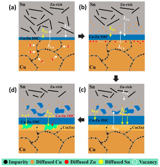
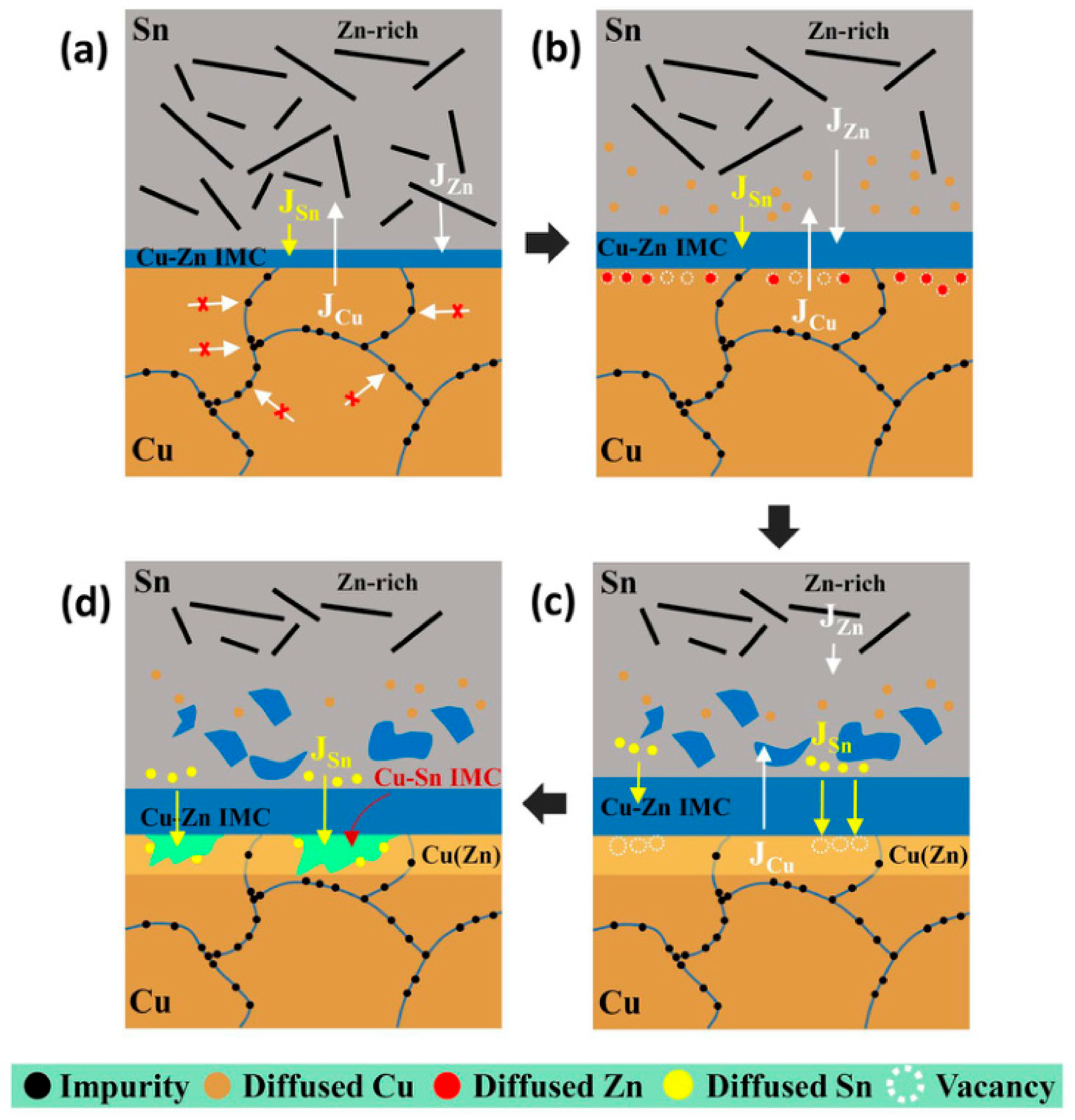
The proposed mechanism for the reduced void formation is shown in Figure 3 [15]. In the initial stage (Figure 3a), impurities at the Cu grain boundaries reduce grain-boundary diffusion, while Cu moves toward the solder through other diffusion paths and Zn diffuses toward Cu to form Cu5Zn8. In Figure 3b, Zn atoms entering the Cu side occupy vacancies and Cu atoms moving toward the solder fill the sites left by Zn, which reduces the vacancy accumulation near the interface. As the aging proceeds, Zn near the interface is consumed for Cu5Zn8 growth and vacancies start to accumulate on the Cu side; Sn diffusion toward Cu also starts (Figure 3c). Finally, part of the Cu-Zn IMC is separated from the original interface and a Cu-Sn IMC is formed between the Cu-Zn phase and Cu (Figure 3d). The mechanism was proposed for the specific materials and aging conditions used in Ref. [15]. A decrease in IMC growth by Zn addition was also reported for a Sn-Bi-Zn/Cu joint [12]. The vacancy-filling explanation was proposed for the Sn-9Zn/PC-Cu joint aged at 175 °C [15]. It has not been fully tested for other temperatures, Cu plating conditions, or solder compositions.
Figure 3.
Schematic of the microstructure evolution of SZ/PC-Cu (high impurity content) during aging at 175 °C (a) Cu and Zn diffusion and initial Cu5Zn8 formation, (b) vacancy filling by Cu and Zn diffusion, (c) vacancy accumulation after Zn consumption, and (d) Cu-Zn IMC separation and Cu-Sn IMC formation (reproduced with permission from Ref. [15]). White arrows with red x mark shows that no Cu diffusion along grain boundaries occurs.
4. Thermo-/Electromigration
4.1. Thermomigration
Thermomigration is important for the fine pitch soldering because a small difference in processing temperature can cause a large gradient of temperature across the solder. Chen et al. discussed that a temperature difference of only 1 °C across a 10 μm microbump corresponds to a temperature gradient of approximately 1000 °C/cm [25]. Such a large gradient can accelerate directional transport of atom that cause different interfacial reactions at the hot and cold ends. In the in-situ observation of Cu/Sn/Cu joints, asymmetric Cu dissolution and IMC growth between the hot and cold ends was observed under a temperature gradient [26].
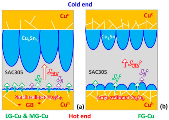
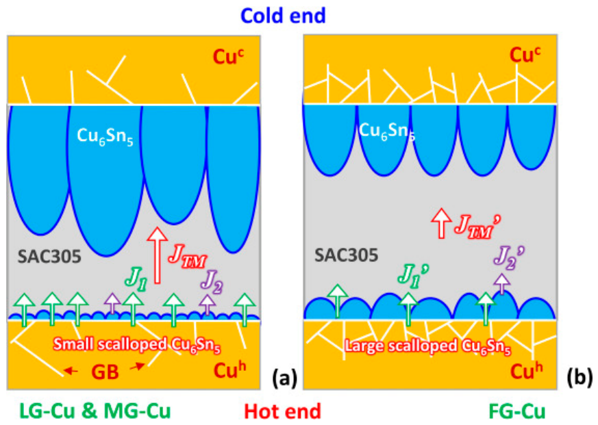
The microstructure of the Cu substrate is another factor affecting the thermomigration behavior [23]. Chung et al. investigated Cu/SAC305/Cu sandwich joints under a temperature gradient of 1753 °C/cm [23]. They observed that Cu dissolved from the hot end and migrated toward the cold end, resulting in enhanced Cu6Sn5 growth at the cold side [23]. The proposed Cu dissolution paths are illustrated in Figure 4. For large-grained (LG)-Cu and micro-grained (MG)-Cu (Figure 4a), small scallop-shaped Cu6Sn5 grains were formed at the hot end. The numerous grain boundaries between the scallops provided fast paths for Cu dissolution, thereby producing a relatively large Cu flux toward the cold end. For fine-grained (FG)-Cu (Figure 4b), a thicker and coarser Cu6Sn5 layer was formed. The reduced number of grain boundaries and the consumption of Cu for local IMC growth decreased further Cu dissolution from the hot-end substrate. Thus, the coarse Cu6Sn5 layer worked as a diffusion barrier and reduced the thermomigration flux toward the cold end [23]. However, the magnitude and the dominant reactions may differ in Sn-Bi and Sn-Zn joints because of the clear interfacial phases and testing conditions [15,23,24].
Figure 4.
Schematic of Cu dissolution and thermomigration flux depending on the hot-end Cu6Sn5 microstructure. (a) LG-Cu and MG-Cu with small scallop-type Cu6Sn5 grains and many grain-boundary diffusion paths. (b) FG-Cu with a coarser Cu6Sn5 layer and reduced Cu flux toward the cold end (reproduced with permission from Ref. [23]).
4.2. Electromigration
Electromigration is also key issue degrading reliability in fine-pitch solder joints, especially operated at high current density [27]. Electron wind drives atoms in one direction, while concentration and stress gradients can produce opposite atomic fluxes. In particular, the electromigration behavior is more complicated in Sn-Bi solder because the Sn-rich and Bi-rich phases have different migration behavior. Current stressing can separate the two phases and produce local Bi-rich regions [27,28,29]. In addition, the Cu transport and IMC formation depend strongly on the metallization and surface finish of the Cu pad.
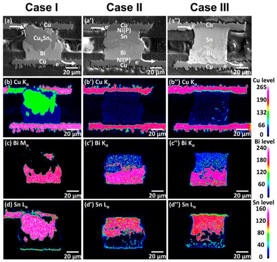
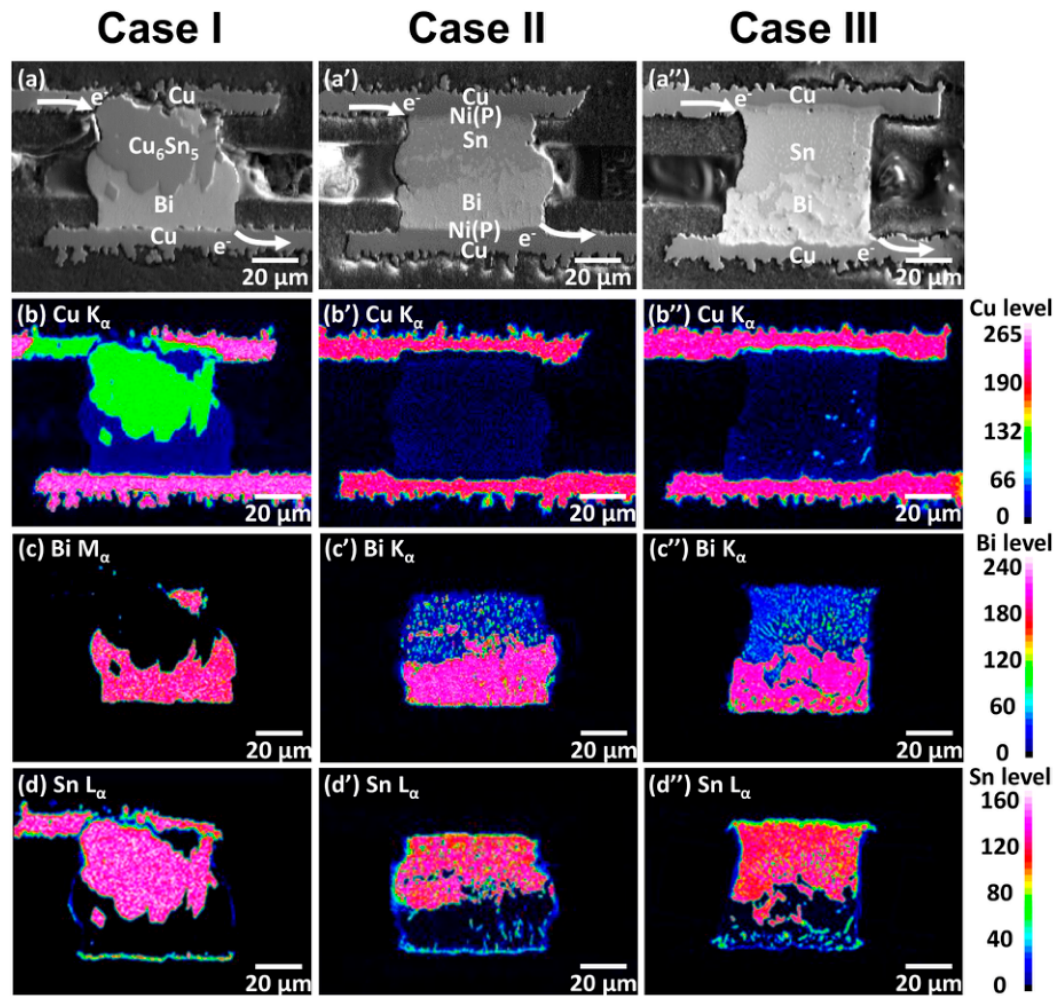
Figure 5 shows the change in microstructure of Sn-58Bi microjoints with organic solderability preservative (OSP), conventional electroless nickel/electroless palladium/immersion gold (ENEPIG), and ultrathin-Ni(P)-type ENEPIG surface finishes under electrical stress at approximately 100 °C and 104 A/cm2 for up to 72 h [24]. The OSP joint showed significant Cu consumption and redistribution of the Sn-rich and Bi-rich phases (Figure 5a–d). In contrast, the conventional ENEPIG joint showed reduced Cu diffusion due to the relatively thick Ni(P) barrier (Figure 5a′–d′). However, the thick barrier increased electrical resistance and Joule heating. The ultrathin-Ni(P)-type ENEPIG joint also suppressed Cu consumption while using a much thinner Ni(P) barrier (Figure 5a″–d″). These results indicate that the barrier thickness is important for controlling both Cu diffusion and electrical resistance in Sn-Bi microjoints. The Bi and Sn elemental maps in Figure 5 show that the portion of Sn-rich and Bi-rich phases changed under the stress by electrical current. This means that electromigration in Sn-Bi microjoints affects not only Cu transport but also the portion of Sn-rich and Bi-rich phases.
Figure 5.
SEM micrographs showing the interior microstructure of micro joints (a–a″) along with FE-EPMA elemental mappings of Cu (b–b″), Bi (c–c″), and Sn (d–d″) after electron current stressing of 104 A/cm2 at 100 ◦C for 72 h: (a–d) Case I: OSP/Sn-58Bi/OSP; (a′–d′) Case II: ENEPIG/Sn-58Bi/ENEPIG; (a″–d″) Case III: ultrathin-Ni(P)-type ENEPIG/Sn-58Bi/ultrathin-Ni(P)-type ENEPIG. (reproduced with permission from Ref. [24]).
Table 2 summarizes the degradation mechanisms discussed so far.
Table 2.
Representative degradation modes of Cu/solder joints and the corresponding design variables.
Table 3 shows the degradation mode and the corresponding design factors. Aging temperature and duration change the microstructure of solders, while temperature gradients and current density drive atomic transport. Additives for Cu plating and methods of surface finishing also influence void formation and Cu consumption [6,7,14,15,18,23,24].
Table 3.
Representative degradation modes of Cu/solder joints.
5. Cu-Cu Direct Bonding for Ultra Fine Pitch
As the interconnection pitch decreases, the solder volume becomes smaller and the IMC can occupy a large part of the joint. Current crowding also becomes more serious in fine-pitch interconnections. Cu-Cu direct bonding and hybrid bonding remove the solder phase and have been studied for very fine-pitch packaging [32,33]. The technologies, however, have different problems from solder joints, including Cu oxidation, surface flatness, void closure, and sufficient atomic diffusion across the bonding interface.
Microstructure control of Cu that can enhance the atomic diffusion at the Cu-Cu interface is a main stream of the study to improve the bonding quality [34,35]. For example, Jhan et al. showed that nanocrystalline Cu with an average grain size of 78 nm produced a maximum shear strength of 71 MPa after bonding at 300 °C in a formic-acid atmosphere [34]. Furthermore, the high bonding temperature of Cu-Cu direct bonding can be reduced by surface activation [36,37,38]. Yu et al. performed Ar plasma treatment for (111)-oriented nanotwinned Cu, which allowed Cu/SiO2 hybrid bonding at 150 °C [36]. In the work by Niu et al., Ar/H2 plasma and citric-acid treatment were used to form bonding at 200 °C in air [37]. He et al. achieved direct Cu-Cu bonding at 100 °C for 60 min or 200 °C for 5 min using a low-impurity nanocrystalline Cu layer after surface cleaning and plasma activation [38]. Although Cu-Cu direct bonding has no solder phase and IMC formation, it requires careful control of surface oxidation, roughness, alignment, and bonding conditions [32,33,34,35,36,37,38] that will increase processing costs. In addition, the characterization of surface energy remains challenging at the nanoscale [39], although surface energy plays an important role in interfacial bonding. Therefore, Cu-Cu bonding is now mainly used for ultra-fine pitch chip-level interconnection.
6. Conclusions
In summary, low-temperature Sn-Bi and Sn-Zn solder systems were reviewed together with the reactions with Cu. Sn-58Bi provides a very low soldering temperature, but the brittle Bi-rich phase and the coarsening of the two-phase microstructure limit its reliability. The addition of Zn and In can reduce part of the coarsening in selected Sn-Bi compositions. Bi addition to Sn-3.5Ag decreased the melting onset by approximately 20 °C, and SAB5 maintained a shear strength of 66 MPa after aging at 150 °C for 144 h. Sn-9Zn-3Bi could also be reflowed at 210 °C and showed approximately 82% spreading and 44.5 MPa shear strength.
In addition to alloy design, the joining process and the Cu interface strongly affect the joint behavior. Electrodeposited Sn/Bi bilayers formed a eutectic-like structure during heating, and a Sn-5Sb/Sn-58Bi mixed solder formed a new final composition during reflow. For Cu/solder interfaces, the initial Cu6Sn5 morphology changed the subsequent IMC growth, and impurities incorporated into electroplated Cu promoted Kirkendall void formation. Sn-9Zn formed Cu5Zn8 and showed much less interfacial voiding than SAC305 for the high-impurity Cu condition.
As the joint size decreases, reliability is also increasingly affected by temperature and current gradients. Thermomigration causes directional Cu transport and asymmetric IMC growth, while electromigration in Sn-Bi joints can induce phase separation and Cu consumption. This indicates that the stability of a fine solder joint depends not only on the solder composition but also on the Cu microstructure and interfacial barrier structure. At still smaller interconnection pitches, Cu-Cu and hybrid bonding provide an alternative approach by removing the solder phase, although their processing conditions and application areas are different from those of low-temperature soldering.
This review highlights that low-temperature joining cannot be determined only by the melting temperature of the solder. The solder microstructure, Cu-pad condition, interfacial reaction, and thermal and electrical loading conditions all change the joint reliability. More systematic studies using the same joint geometry and well-defined thermal and current histories will be useful for comparing different low-temperature solder systems and for selecting the appropriate joining material for each package structure.
Author Contributions
E.K., S.L. (Sujith Lal), O.A.P., C.-M.C., B.L., S.L. (Sooman Lim) and B.H. organized the structure of the manuscript. E.K., S.L. (Sujith Lal), O.A.P., C.-M.C., B.L., S.L. (Sooman Lim) and B.H. wrote the whole manuscript. All authors collaboratively wrote the manuscript. All authors have read and agreed to the published version of the manuscript.
Funding
This research was supported by the Chung-Ang University Research Grants in 2024. This research was supported by the Glocal University 30 Project at Jeonbuk National University in 2026 (JBNU-GU30-2026).
Institutional Review Board Statement
Not applicable.
Informed Consent Statement
Not applicable.
Data Availability Statement
No new data were created or analyzed in this study. Data sharing is not applicable to this article.
Conflicts of Interest
The authors declare no conflicts of interest.
References
- Choi, S.; Chen, C.-M.; Hwang, B. Cu-Cu mechanical bonding for 3D integration of the next generation electronic chips: Interfacial mechanisms, surface engineering, and emerging low-temperature strategies. Facta Univ. Ser. Mech. Eng. 2025, 23, 921–943. [Google Scholar] [CrossRef] [Scilit]
- Kotadia, H.R.; Howes, P.D.; Mannan, S.H. A review: On the development of low melting temperature Pb-free solders. Microelectron. Reliab. 2014, 54, 1253–1273. [Google Scholar] [CrossRef] [Scilit]
- Ha, H.; Choi, S.; Baumli, P.; Chen, C.-M.; Hwang, B. Surface-energy-driven selective soldering of Sn-58Bi on holey polyimide for low-temperature, robust flexible interconnects. Facta Univ. Ser. Mech. Eng. 2026, 24, 275–288. [Google Scholar] [CrossRef] [Scilit]
- Xu, K.-K.; Zhang, L.; Gao, L.-L.; Jiang, N.; Zhang, L.; Zhong, S.-J. Review of microstructure and properties of low temperature lead-free solder in electronic packaging. Sci. Technol. Adv. Mater. 2020, 21, 689–711. [Google Scholar] [CrossRef] [Scilit] [PubMed]
- Li, Y.; Li, Y.-J.; Chung, M.-H.; Chen, C.-M. Microstructures of Sn-5Sb/Sn-58Bi mixed solder and its interfacial reaction with copper. J. Mater. Sci. Mater. Electron. 2025, 36, 469. [Google Scholar] [CrossRef] [Scilit]
- Lee, J.-Y.; Chen, C.-M. Effects of Initial Morphology on Growth Kinetics of Cu6Sn5 at SAC305/Cu Interface during Isothermal Aging. Materials 2022, 15, 4751. [Google Scholar] [CrossRef] [Scilit] [PubMed]
- Raeder, C.H.; Felton, L.E.; Tanzi, V.A.; Knorr, D.B. The effect of aging on microstructure, room temperature deformation, and fracture of Sn-Bi/Cu solder joints. J. Electron. Mater. 1994, 23, 611–617. [Google Scholar] [CrossRef] [Scilit]
- Mokhtari, O.; Nishikawa, H. Correlation between microstructure and mechanical properties of Sn–Bi–X solders. Mater. Sci. Eng. A 2016, 651, 831–839. [Google Scholar] [CrossRef] [Scilit]
- Hirata, Y.; Yang, C.-H.; Lin, S.-K.; Nishikawa, H. Improvements in mechanical properties of Sn–Bi alloys with addition of Zn and In. Mater. Sci. Eng. A 2021, 813, 141131. [Google Scholar] [CrossRef] [Scilit]
- Nishikawa, H.; Hirata, Y.; Yang, C.-H.; Lin, S.-K. Effect of Low Bi Content on Reliability of Sn-Bi Alloy Joints Before and After Thermal Aging. JOM 2022, 74, 1751–1759. [Google Scholar] [CrossRef] [Scilit]
- Zhou, S.; Mokhtari, O.; Rafique, M.G.; Shunmugasamy, V.C.; Mansoor, B.; Nishikawa, H. Improvement in the mechanical properties of eutectic Sn58Bi alloy by 0.5 and 1 wt% Zn addition before and after thermal aging. J. Alloys Compd. 2018, 765, 1243–1252. [Google Scholar] [CrossRef] [Scilit]
- Mokhtari, O.; Zhou, S.; Chan, Y.C.; Nishikawa, H. Effect of Zn Addition on Interfacial Reactions Between Sn-Bi Solder and Cu Substrate. Mater. Trans. 2016, 57, 1272–1276. [Google Scholar] [CrossRef] [Scilit]
- Shang, M.; Li, C.; Wang, Y.; Chen, X.; Zhao, Y.; Ke, J.; Wang, Y.; Ma, H.; Chen, J. IMC growth mechanism of Sn58Bi/Cu solder joints and its effect on the coarsening of the Bi phase. J. Mater. Res. Technol. 2024, 33, 6307–6318. [Google Scholar] [CrossRef] [Scilit]
- Shen, Y.-A.; Kao, H.-Z.; Liang, C.-M.; Chen, C.-M.; Ho, C.-E.; Oh, M.; Hsiao, C.-Y. Enabling reliable 210 °C reflow through Bi-modified Sn–9Zn alloy: Wettability, interfacial reactions, and joint strength. Mater. Sci. Semicond. Process. 2026, 211, 110766. [Google Scholar] [CrossRef] [Scilit]
- Shen, Y.-A.; Lin, C.-Y.; Chen, C.-M. Exploring mechanism of suppressing void formation at Interface of Sn–9Zn and Cu. J. Mater. Sci. Mater. Electron. 2024, 35, 778. [Google Scholar] [CrossRef] [Scilit]
- Pstruś, J. Early stages of wetting of copper by Sn–Zn eutectic alloy. J. Mater. Sci. Mater. Electron. 2018, 29, 20531–20545. [Google Scholar] [CrossRef] [Scilit]
- Liu, H.; Wei, Y.; Zhang, Y.; Hou, Z.; Zhao, X. Effects of Bi and Cu addition on mechanical properties of Sn9Zn alloy and interfacial intermetallic growth with Ni substrate. Mater. Today Commun. 2023, 35, 106350. [Google Scholar] [CrossRef] [Scilit]
- Su, Y.-J.; Tsai, K.-L.; Li, Y.-J.; Chen, C.-M. Effects of suppressors on the incorporation of impurities and microstructural evolution of electrodeposited Cu solder joints. J. Taiwan Inst. Chem. Eng. 2023, 149, 104956. [Google Scholar] [CrossRef] [Scilit]
- Chen, P.-K.; Li, Y.-J.; Yen, Y.-W.; Chen, C.-M. Influences of Impurity Incorporation in Electroplated Cu on the SnAgCu and Ni-Containing SnAgCu Solder Joints. J. Electrochem. Soc. 2022, 169, 052508. [Google Scholar] [CrossRef] [Scilit]
- Wang, J.; Chen, J.; Zhang, L.; Zhang, Z.; Han, Y.; Hu, X.; Lu, H.; Zhang, S. Forming mechanism and growth of Kirkendall voids of Sn/Cu joints for electronic packaging: A recent review. J. Adv. Join. Process. 2022, 6, 100125. [Google Scholar] [CrossRef] [Scilit]
- Borgesen, P.; Yin, L.; Kondos, P. Assessing the risk of “Kirkendall voiding” in Cu3Sn. Microelectron. Reliab. 2011, 51, 837–846. [Google Scholar] [CrossRef] [Scilit]
- Kim, S.; Yu, J. Effects of Ag on the Kirkendall void formation of Sn–xAg/Cu solder joints. J. Appl. Phys. 2010, 108, 083532. [Google Scholar] [CrossRef] [Scilit]
- Chung, M.-H.; Yu, C.-H.; Choi, C.; Choi, S.; Hwang, B.; Ho, C.-E.; Shen, Y.-A.; Chen, C.-M. Suppression of thermomigration in Cu/Sn-3Ag-0.5Cu/Cu solder joints by grain coarsening of Cu6Sn5 at hot end. J. Taiwan Inst. Chem. Eng. 2026, 187, 106717. [Google Scholar] [CrossRef] [Scilit]
- Yang, Z.-Y.; Hsieh, W.-Z.; Lee, C.-Y.; Chen, K.-J.; Chen, C.-M.; Shen, Y.-A.; Ho, C.-E. Electromigration reliability of low-temperature Bi-Sn micro joints with different surface coatings over Cu pads. Vacuum 2026, 252, 115461. [Google Scholar] [CrossRef] [Scilit]
- Chen, C.; Hsiao, H.-Y.; Chang, Y.-W.; Ouyang, F.; Tu, K.N. Thermomigration in solder joints. Mater. Sci. Eng. R Rep. 2012, 73, 85–100. [Google Scholar] [CrossRef] [Scilit]
- Qu, L.; Zhao, N.; Ma, H.; Zhao, H.; Huang, M. In situ study on the effect of thermomigration on intermetallic compounds growth in liquid-solid interfacial reaction. J. Appl. Phys. 2014, 115, 204907. [Google Scholar] [CrossRef] [Scilit]
- Li, W.; Guo, L.; Li, D.; Liu, Z.-Q. Research Overview on the Electromigration Reliability of SnBi Solder Alloy. Materials 2024, 17, 2848. [Google Scholar] [CrossRef] [Scilit] [PubMed]
- Chen, L.-T.; Chen, C.-M. Electromigration study in the eutectic SnBi solder joint on the Ni/Au metallization. J. Mater. Res. 2006, 21, 962–969. [Google Scholar] [CrossRef] [Scilit]
- Chen, C.-M.; Huang, C.-C. Effects of silver doping on electromigration of eutectic SnBi solder. J. Alloys Compd. 2008, 461, 235–241. [Google Scholar] [CrossRef] [Scilit]
- Shen, Y.-A.; Chen, F.-Y.; Gao, R.; Ho, C.-E.; Nishikawa, H.; Chen, C.-M. Effect of Bi Addition on Melting Behavior, Solder Joint Strength, and Thermal Aging Resistance of Sn-3.5Ag/Cu Joints. JOM 2025, 77, 4206–4214. [Google Scholar] [CrossRef] [Scilit]
- Wang, W.-L.; Cherng, S.-J.; Huang, Y.-T.; Gao, R.; Tatsumi, H.; Nishikawa, H.; Chen, C.-M. Low-temperature soldering using Sn/Bi electrodeposited bilayer. Mater. Sci. Semicond. Process. 2025, 186, 109056. [Google Scholar] [CrossRef] [Scilit]
- Hu, H.-W.; Chen, K.-N. Development of low temperature CuCu bonding and hybrid bonding for three-dimensional integrated circuits (3D IC). Microelectron. Reliab. 2021, 127, 114412. [Google Scholar] [CrossRef] [Scilit]
- Panigrahy, A.K.; Chen, K.-N. Low Temperature Cu–Cu Bonding Technology in Three-Dimensional Integration: An Extensive Review. J. Electron. Packag. 2018, 140, 010801. [Google Scholar] [CrossRef] [Scilit]
- Jhan, J.-J.; Wataya, K.; Nishikawa, H.; Chen, C.-M. Electrodeposition of nanocrystalline Cu for Cu-Cu direct bonding. J. Taiwan Inst. Chem. Eng. 2022, 132, 104127. [Google Scholar] [CrossRef] [Scilit]
- Chang, J.-S.; Song, J.-M.; Chen, C.-M. Unidirectional cross-interface grain growth in Cu–Cu direct bonding. J. Mater. Res. Technol. 2025, 38, 2212–2219. [Google Scholar] [CrossRef] [Scilit]
- Yu, M.-H.; Ong, J.-J.; Tran, D.-P.; Chiu, W.-L.; Hsu, W.-Y.; Lin, H.-E.; Chen, Y.-A.; Tseng, H.-H.; Shen, G.-Y.; Yang, S.-C.; et al. Low temperature Cu/SiO2 hybrid bonding via (111)-oriented nanotwinned Cu with Ar plasma surface modification. Appl. Surf. Sci. 2023, 636, 157854. [Google Scholar] [CrossRef] [Scilit]
- Niu, F.; Wang, X.; Yang, S.; Xu, S.; Zhang, Y.; Suga, T.; Wang, C. Low-temperature Cu/SiO2 hybrid bonding based on Ar/H2 plasma and citric acid cooperative activation for multi-functional chip integration. Appl. Surf. Sci. 2024, 648, 159074. [Google Scholar] [CrossRef] [Scilit]
- He, C.; Zhou, J.; Zhou, R.; Chen, C.; Jing, S.; Mu, K.; Huang, Y.-T.; Chung, C.-C.; Cherng, S.-J.; Lu, Y.; et al. Nanocrystalline copper for direct copper-to-copper bonding with improved cross-interface formation at low thermal budget. Nat. Commun. 2024, 15, 7095. [Google Scholar] [CrossRef] [Scilit] [PubMed]
- Ha, H.; Mueller, S.; Guriyanova, S.; Hwang, B. Surface energy characterization of a single microsphere particle using PeakForce quantitative nanomechanical mapping mode of atomic force microscope. Facta Univ. Ser. Mech. Eng. 2025, 23, 171–181. [Google Scholar] [CrossRef] [Scilit]

Disclaimer/Publisher’s Note: The statements, opinions and data contained in all publications are solely those of the individual author(s) and contributor(s) and not of MDPI and/or the editor(s). MDPI and/or the editor(s) disclaim responsibility for any injury to people or property resulting from any ideas, methods, instructions or products referred to in the content. |
© 2026 by the authors. Licensee MDPI, Basel, Switzerland. This article is an open access article distributed under the terms and conditions of the Creative Commons Attribution (CC BY) license.