


Abstract
To achieve efficient solar-to-electricity conversion, third-generation photovoltaics represented by perovskite solar cells (PSCs) have attracted tremendous interest. However, perovskites are vulnerable to humidity, oxygen and heat, and insufficient device stability hinders their commercialization. Polyimides (PIs), polymers with facile preparation and superior comprehensive properties, are widely used in electronics for their great mechanical strength, high-temperature tolerance and biocompatibility. PIs exhibit good moisture and oxidation resistance under harsh conditions, which well offsets perovskites’ intrinsic environmental-sensitivity drawback and makes PIs promising candidates for solving the stability bottleneck of PSCs. Herein, three fluorinated transparent PIs were synthesized through molecular-structure design and adopted as flexible substrates and auxiliary modification layers for self-assembled monolayers (SAMs). The 6FDA-TFMB film shows a maximum visible-light transmittance of 90.7%, a 5% weight-loss temperature above 400 °C and a glass-transition temperature of 339 °C, and flexible PSCs based on it obtain a power conversion efficiency (PCE) of 18.06%. Hydroxyl-containing 6FDA-6FAP was further used to construct PI/SAM composite hole-selective layers, which suppress SAM aggregation, increase SAM anchoring coverage on ITO, optimize perovskite crystallization and passivate buried-interface defects. Rigid 1.68 eV wide-bandgap perovskite devices with this composite interface deliver a PCE improvement from 22.48% to 23.15% with greatly enhanced thermal and environmental stability. This work demonstrates that transparent heat-resistant PIs can act as both high-performance flexible substrates and synergistic buried-interface regulators, providing new material strategies for efficient, stable perovskite photovoltaics.
1. Introduction
Photovoltaic technologies have undergone rapid development in the global transition toward low-carbon energy systems. As the most mature photovoltaic technology, conventional crystalline-silicon solar cells have achieved large-scale commercialization. Nevertheless, they still suffer from drawbacks including high manufacturing costs, complicated production procedures, and considerable energy consumption [1]. Furthermore, their theoretical efficiency limit is approximately 29.4%, leaving limited room for further performance improvement. Later-developed CdTe (cadmium telluride) [2] and CIGS (copper-indium-gallium-selenide) [3] thin-film technologies deliver certain improvements in device weight reduction and flexibility enhancement, yet they are still plagued by cumbersome fabrication processes, the use of scarce or toxic elements, and insufficient environmental friendliness. Such limitations of traditional photovoltaic technologies have paved the way for the emergence of next-generation photovoltaic techniques. Against this backdrop, third-generation photovoltaic technologies, represented by perovskite solar cells (PSCs), have advanced rapidly [4]: independently certified efficiencies now exceed 27% [5], and laboratory-scale inverted devices have reached 26.31% [6].
As organic–inorganic hybrid optoelectronic materials, perovskites offer compelling advantages, including a tunable bandgap [7], a high absorption coefficient, a favorable crystal structure [8], and a long carrier diffusion length [9], demonstrating enormous application potential in photovoltaics. In little more than one decade, the power-conversion efficiency (PCE) of PSCs has increased from an initial value of 3.8% to over 27%, which is comparable to that of crystalline-silicon solar cells. Beyond high efficiency, perovskite materials can be fabricated via low-temperature solution processing, substantially reducing production costs. Meanwhile, perovskite solar cells based on flexible substrates hold broad application prospects in building-integrated photovoltaics, wearable electronics, and other fields [10]. However, perovskite materials are rather sensitive to moisture, oxygen, and thermal conditions, and device stability remains a critical bottleneck restricting their further commercial deployment [10].
Polyimides (PIs) are a family of polymeric materials featuring facile fabrication routes and excellent comprehensive properties that make them promising candidates to address this stability bottleneck. Owing to their outstanding mechanical performance, high-temperature resistance, and biocompatibility, polyimides have been widely adopted in electronic devices [11]. The stable imide-ring structure in their molecular backbones endows polyimides with superior thermal stability (glass-transition temperature generally above 250 °C), along with good moisture and oxidation resistance, enabling them to withstand harsh environments such as high temperature, high humidity, and oxygen exposure [12]. These unique advantages well complement the high environmental susceptibility and poor stability of perovskites, positioning PIs as promising candidate materials for stabilizing PSC devices.
For photovoltaic applications, optical transparency is as critical as thermal stability. The intrinsic coloration of aromatic polyimides originates from intermolecular charge-transfer complexes (CTCs) between dianhydride and diamine segments; molecular-engineering strategies such as fluorination, bulky pendant groups, and ladder-type dianhydrides can effectively suppress CTC formation and yield colorless transparent polyimide (cPI) films [13,14], whose photo-oxidation mechanisms have recently been elucidated [15]. State-of-the-art colorless polyimides now combine high visible-light transmittance with ultra-low coefficients of thermal expansion [16] and ultra-high glass-transition temperatures [12], while polyimide aerogels further demonstrate strong moisture resistance [17,18]. Beyond serving as passive substrates, polyimides are increasingly exploited as functional components in PSCs: ultrathin colorless polyimide foils have enabled lightweight flexible PSCs with a PCE of 15.52% [19]; polyimide-based flexible transparent electrodes have been integrated into double-sided devices and heaters [20]; polyimide and polyamic-acid additives improve photovoltaic performance [21]; in situ polymerized copolymer networks enhance device stability [22]; and a fluorinated polyimide tunneling layer has delivered 24.61% efficiency [23]. Very recently, an ultra-thin carbon-nanotube-embedded polyimide transparent conductor built on the same 6FDA-TFMB chemistry enabled foldable PSCs with 18.72% efficiency [24], and a UV-absorbing colorless polyimide substrate combined with photon downshifting raised flexible PSC efficiency to 20.4% while imparting UV resistance [25]. These advances highlight the versatile roles of transparent polyimides in perovskite photovoltaics.
Despite this progress, two challenges remain. First, conventional polymer substrates such as PET cannot withstand the high temperatures involved in device fabrication, so the thermal stability of flexible substrates must be further improved. Second, in state-of-the-art inverted (p-i-n) devices, self-assembled monolayers (SAMs) have become the dominant hole-selective contact since the first demonstration of 17.8% efficiency [26] and are now widely adopted [27,28]. However, SAM molecules tend to self-aggregate in solution and anchor inhomogeneously on transparent conductive oxides, leading to incomplete surface coverage and buried-interface defects that limit both efficiency and stability [29]. This issue is particularly severe for wide-bandgap perovskites [30,31], where non-radiative recombination at the buried interface directly costs open-circuit voltage and fill factor. Strategies including co-assembly with auxiliary molecules [32], amine-rich cross-linking templates [33], and fully polymeric self-assembled layers [34] have been developed to improve SAM coverage and homogeneity; complementary approaches such as self-assembling composite designs [35], co-self-assembled reconstruction [36], coverage reinforcement [37], and buried-interface stabilization [38] have further advanced the field, as summarized in recent reviews [39], and uniform SAMs are now enabling high-efficiency tandem-compatible devices [40,41].
In this work, a series of fluorine-containing, transparent, high-temperature-resistant polyimides were synthesized through molecular-structure design and investigated as both flexible substrates and interfacial regulators for PSCs. Among them, 6FDA-TFMB combines excellent optical transmittance and thermal stability; using this polymer, IZO-integrated composite conductive flexible substrates were prepared, and flexible PSCs with an efficiency of 18.06% were realized. Furthermore, the synergistic effect of multiple functional groups on 6FDA-6FAP segments drives dense and uniform chemical anchoring of mixed SAMs on the ITO surface. Mechanistic investigations reveal that long polyimide chains effectively suppress SAM agglomeration. Moreover, groups such as carbonyl groups realize efficient passivation of interfacial defects, yielding marked improvements in both efficiency and stability of photovoltaic devices. Based on this composite interface, rigid wide-bandgap perovskite devices achieve a PCE of 23.15%, accompanied by substantial enhancements in multiple stability metrics. In summary, this work shows that transparent polyimides can serve as both high-performance flexible substrates and interfacial-modification materials. It expands the multi-dimensional applications of polyimides in perovskite photovoltaics and provides new strategies for developing high-efficiency, long-lifespan perovskite optoelectronic devices.
2. Materials and Methods
2.1. Materials
All chemical reagents were used as received without further purification. N,N-dimethylacetamide (DMAC, 99.9%), dimethyl sulfoxide (DMSO, 99.9%), N,N-dimethylformamide (DMF, 99.9%), isoquinoline (99.8%), pyridine (99.8%), anhydrous ethanol (95%), acetone (95%), diethyl ether (95%), methanol (95%), lead bromide (PbBr2, 99.99%), lead iodide (PbI2, 99.99%), cesium iodide (CsI, 99.99%), isopropanol (IPA, 99.8%) and ethyl acetate (95%) were purchased from InnoChem (Beijing Innochem Science & Technology Co., Ltd.), Beijing, China. m-Cresol (99.8%) was obtained from Sigma-Aldrich (Shanghai) Trading Co., Ltd., Shanghai, China. 4,4′-(Hexafluoroisopropylidene)diphthalic anhydride (6FDA, 99.8%), 4,4′-((perfluoropropane-2,2-diyl)bis(4,1-phenylene))bis(oxy)dianiline (HFPB, 99.8%), 2,2-bis(3-amino-4-hydroxyphenyl)hexafluoropropane (6FAP, 99.9%) and 2,2′-bis(trifluoromethyl)-4,4′-diaminobiphenyl (TFMB, 99.8%) were supplied by CHINATECH (Tianjin Zhongtai Material Technology Co., Ltd.), Tianjin, China. The IZO sputtering target (99.99%) was purchased from DinaKe Fine Materials (Jiangsu Temch Fine Materials Co., Ltd.), Nanjing, China (4-(7H-Dibenzo[c,g]carbazol-7-yl)butyl)phosphonic acid (4PADCB, 99.9%) was obtained from Jiuyao Optoelectronic (Wuhan Jiuyao Optoelectronic Technology Co., Ltd.), Wuhan, China. Formamidinium acetate, methylammonium chloride (MACl, 99%), formamidinium iodide (FAI, 99%) and methylammonium bromide (MABr, 99%) were self-synthesized. Silver (Ag, 99.999%) was purchased from Zhongjiao Jinyuan (Beijing China Education Au-light Co., Ltd.), Beijing, China. ITO conductive glass (8 Ω/sq) was supplied by Liaoning Youxuan (Liaoning Youxuan New Energy Technology Co., Ltd.), Yingkou, China.
2.2. Synthesis of Fluorine-Containing Polyimides
Before polymerization, diamine and dianhydride monomers were dried in a vacuum oven to remove residual moisture. The polyimides were prepared either by a one-pot procedure or by a chemical imidization route [42], as detailed below and illustrated in Figure S1.
2.2.1. Synthesis of 6FDA-6FAP
A dry 250 mL three-neck flask equipped with mechanical stirring and nitrogen protection was charged with 4.442 g 6FDA, 3.663 g 6FAP, and 40 mL m-cresol. The mixture was heated to 100 °C, 2–3 drops of isoquinoline were added as catalyst, and then the temperature was raised to 180 °C and kept for 8–12 h. After cooling to room temperature, the polymer solution was slowly added to a methanol–water mixture for precipitation. The crude product was redissolved in DMF (15 wt%) and reprecipitated from methanol three times to purify it. The precipitate was filtered and dried under vacuum at 80 °C to obtain 6FDA-6FAP powder. The successful synthesis was confirmed by 1H NMR spectroscopy (Figure S5).
2.2.2. Synthesis of 6FDA-TFMB
A total of 4.442 g 6FDA and 3.202 g TFMB was added to a 250 mL dry nitrogen-purged reactor together with 38 mL DMAC. The mixture was stirred at room temperature for 12 h. Pyridine (catalyst) and acetic anhydride (dehydrating agent) were added sequentially, and then the mixture was heated to 120 °C for 4 h to drive chemical imidization. After cooling, the solution was precipitated in a methanol–water solution and purified by repeated DMF–methanol dissolution–precipitation cycles (three times). The solid was filtered and vacuum-dried at 80 °C to yield 6FDA-TFMB. The chemical structure was verified by 1H NMR spectroscopy (Figure S3).
2.2.3. Synthesis of 6FDA-HFPB
A total of 4.283 g 6FDA and 5.185 g HFPB was dissolved in 37 mL m-cresol in a nitrogen-protected 250 mL flask. After 12 h of stirring at ambient temperature, pyridine and acetic anhydride were introduced, and the reaction proceeded at 120 °C for 4 h. The post-treatment procedure (precipitation, washing, filtration, and vacuum drying at 80 °C) was identical to that described above for the other polyimide samples, and the structure was verified by 1H NMR spectroscopy (Figure S4).
2.3. Fabrication of Polyimide Films and Flexible Conductive Substrates
2.3.1. Preparation of Polyimide Films
The polyimide solution was blade-cast onto clean glass substrates. The wet films were first heated at 80 °C for 6–8 h to slowly evaporate most of the solvent. Afterward, gradient vacuum thermal imidization was performed up to 250 °C with a holding time of ≥8 h to complete cyclization. After cooling to room temperature, the films were peeled off by immersion in deionized water. The final thickness of the freestanding PI films was controlled within 60–90 μm.
2.3.2. Preparation of Flexible IZO/PI Conductive Substrates
Magnetron sputtering equipment (TRP450B, Shenyang Scientific Instrument (SKY Technology Development Co., Ltd., CAS), Shenyang, China, CAS) was employed to deposit the IZO transparent conductive layer; sputter-induced damage was minimized by optimized pre-sputtering, as sputter damage can otherwise introduce recombination losses at the electrode interface [43]. The 6FDA-TFMB polyimide film was fixed on the substrate holder. The target–substrate distance was adjusted to 70–100 mm. The chamber was evacuated to a base vacuum better than 1.2 × 10⁻⁴ Pa. Argon was used as the working gas, and the working pressure was stabilized between 0.1 and 5 Pa. Pre-sputtering was carried out under an RF power of 20–60 W to clean the target surface. Formal sputtering deposition was then performed to obtain flexible IZO/PI composite conductive substrates.
2.4. Fabrication of Perovskite Solar Cells
2.4.1. Solution Preparation
Mixed SAM hole-transporting solution: Under a nitrogen atmosphere inside a glovebox, 6FDA-6FAP was dissolved in DMF to prepare a 1 mg·mL−1 stock solution, and 4PADCB was dissolved in ethanol to prepare a 1 mg·mL−1 stock solution. Both solutions were stirred at 60 °C for 12 h. Afterward, the 6FDA-6FAP solution and the 4PADCB solution were mixed at a volume ratio of 1:10 and stirred at 25 °C for another 2 h. For the control group, only the 4PADCB ethanol solution (1 mg·mL−1) was used.
Perovskite precursor solution: CsI, FAI, MABr, MACl, PbBr2 and PbI2 were dissolved in a mixed solvent of DMF:DMSO = 4:1 (v/v) to prepare a 1.6 mol·L−1 perovskite precursor with the stoichiometry Cs0.05(MA0.17FA0.83)0.95Pb(I0.83Br0.17)3. A 50 μL portion of CsI solution (1.5 mg·mL−1) was added to the precursor, then stirred for 24 h and filtered through a 0.45 μm PTFE filter before use. PDAI2 (1 mg·mL−1 in isopropanol) served as the surface passivation reagent.
2.4.2. Device Manufacturing
ITO glass was patterned by laser etching, then sequentially ultrasonically cleaned in detergent solution, deionized water, and ethanol for 15–20 min each, and dried in an oven at 60 °C. Substrates were treated with UV-ozone for 15 min and transferred into an N2-filled glovebox.
The ITO substrate was preheated at 105 °C for 5–10 min. Then, 80 μL of SAM (or mixed SAM) solution was dropped onto the ITO and spin-coated at 3000 rpm for 20 s, followed by annealing at 105 °C for 10 min and cooling to room temperature. Subsequently, 100 μL of perovskite precursor solution was spin-coated at 3500 rpm for 40 s, and 120 μL of ethyl acetate antisolvent was dropped during the last 15 s of spinning. The as-cast film was annealed at 105 °C for 30 min. After cooling, 50 μL of PDAI2 passivation solution was spin-coated at 5000 rpm for 20 s and annealed at 105 °C for 10 min.
The samples were transferred to a high-vacuum thermal evaporation chamber (Guangtuo Optoelectronic (Suzhou Guangtuo Technology Co., Ltd.), Suzhou, China). Sequential thermal evaporation was performed to deposit 1.5 nm LiF, 25 nm C60, 5 nm BCP, and, finally, an 80 nm Ag electrode through a shadow mask. For flexible perovskite devices, IZO/6FDA-TFMB flexible conductive film replaced ITO glass as the substrate, and the subsequent layer-deposition procedures remained identical. The active area of the device was 0.1 cm2.
2.4.3. Formula for Calculating the Effective Coverage Rate
ip,o = (n2F2AΓ*v)/(4RTNA)
3. Results and Discussion
3.1. Molecular Structure and Molecular Weight of the Polyimides
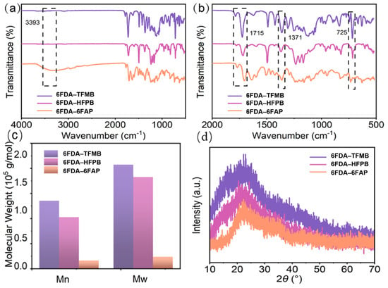
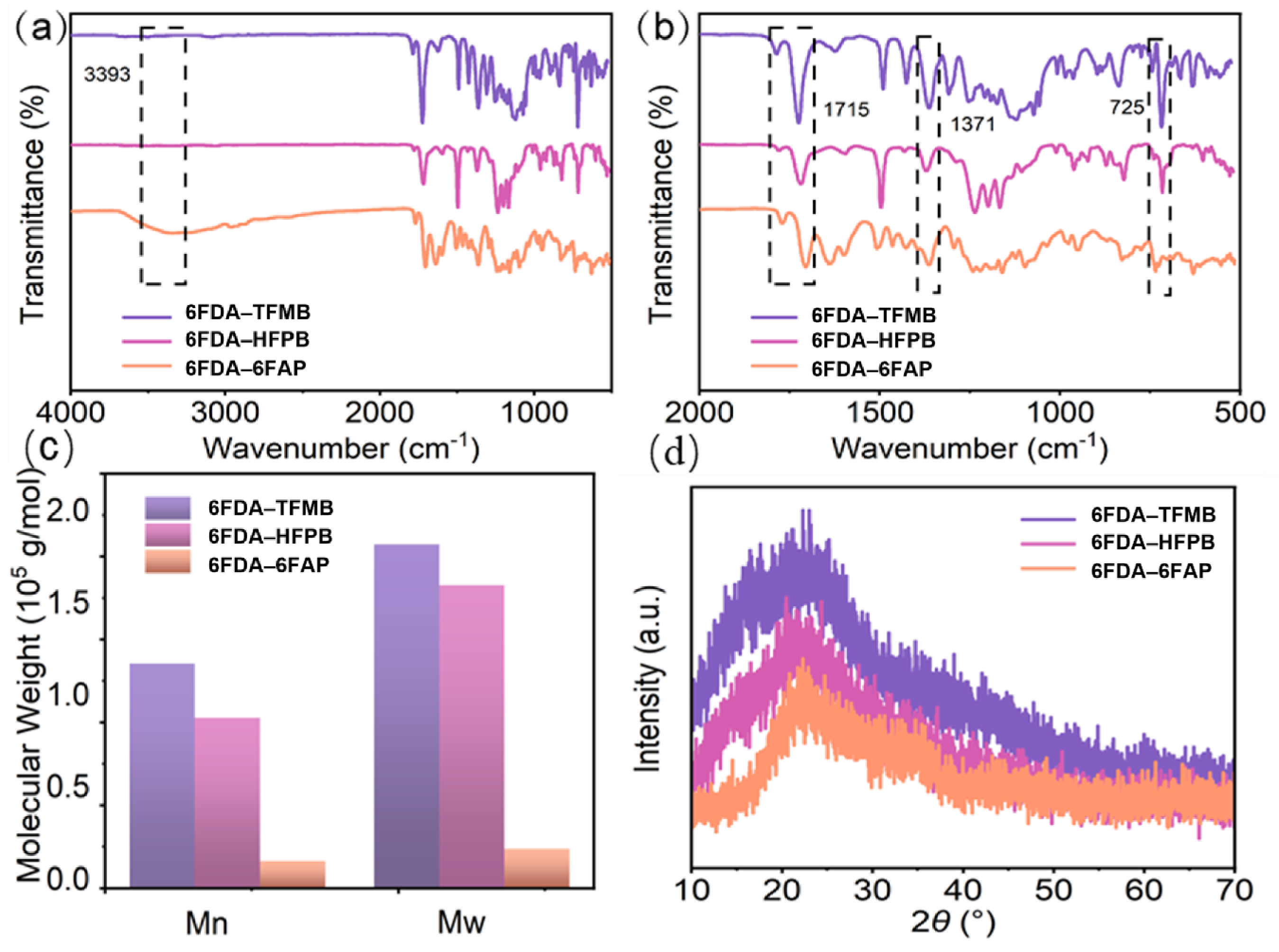
Figure 1a,b presents the FTIR spectra of the three PI films. The absence of the amide N–H stretch peak at 3393 cm−1 confirms the complete imidization of the poly(amic acid) precursors. Characteristic imide peaks at 1715 cm−1 (asymmetric C=O stretch), 1371 cm−1 (C–N stretch), and 725 cm−1 (imide ring bending) are observed for all samples, verifying successful polyimide synthesis.
Figure 1.
(a,b) FTIR spectra of 6FDA-TFMB, 6FDA-HFPB and 6FDA-6FAP films. (c) Molecular weights of 6FDA-TFMB, 6FDA-HFPB and 6FDA-6FAP. (d) XRD patterns of the three PI films.
GPC results (Figure 1c and Table S1) show that all polymers possess appreciable number-average (Mn) and weight-average (Mw) molecular weights. 6FDA-TFMB exhibits the highest molecular weights, followed by 6FDA-HFPB, while 6FDA-6FAP shows substantially lower Mn and Mw owing to the differing monomer reactivity. High molecular weight facilitates continuous, defect-free polymer films, supporting the use of 6FDA-TFMB as the flexible substrate in this work.
XRD patterns (Figure 1d and Table S2) characterize the aggregation structures of the three polyimides. All samples show broad diffused halos without sharp crystalline peaks, confirming amorphous polyimide structures, with diffraction maxima near 2θ ≈ 20°. The diffraction intensity follows the order 6FDA-TFMB > 6FDA-HFPB > 6FDA-6FAP, suggesting tighter chain packing for 6FDA-TFMB and larger interchain spacing for 6FDA-6FAP. These packing differences influence film compactness, charge transport and mechanical properties.
3.2. Thermal Stability and Optical Transparency
The thermal stability of the three polyimide films (6FDA-TFMB, 6FDA-HFPB and 6FDA-6FAP) was characterized by TGA (Figure S2a). All samples undergo one-step thermal degradation. As summarized in Table S3, the 5% weight-loss temperatures (Td5%) of 6FDA-TFMB and 6FDA-HFPB reach 514.1 and 506.8 °C, respectively, whereas 6FDA-6FAP exhibits a distinctly lower Td5% of 431.3 °C. All three values exceed 400 °C, confirming good thermal stability for optoelectronic device fabrication.
DSC was used to determine the glass-transition temperature (Tg) (Figure S2b–e). Clear glass-transition signals are observed for all three polyimides. As listed in Table S3, the Tg values follow the order 6FDA-TFMB (339.0 °C) > 6FDA-6FAP (258.8 °C) > 6FDA-HFPB (244.7 °C). The highest Tg of 6FDA-TFMB arises from its rigid biphenyl skeleton, where aromatic moieties suppress chain rotation and enhance thermal dimensional stability; the comparatively higher Tg of 6FDA-6FAP than 6FDA-HFPB may be attributed to hydrogen bonding between its hydroxyl groups, whereas the flexible ether linkages in 6FDA-HFPB enhance chain mobility.
UV–vis transmittance spectra were recorded to evaluate the optical performance (Figure S2f). The three polyimides show different absorption cutoff wavelengths (Table S4). 6FDA-TFMB has the shortest cutoff (355 nm) and the highest visible transmittance (90.7%), followed by 6FDA-HFPB; 6FDA-6FAP displays a red-shifted absorption edge. These optical differences stem from varied conjugation levels and charge-transfer complex (CTC) formation between the dianhydride and diamine segments. The inset magnifies the absorption edge to clearly resolve their cutoff positions. Combined high transmittance and favorable thermal properties make these polyimides suitable for optoelectronic applications.
3.3. Electronic Structure of the Polyimide Repeating Units
To rationalize these optical differences at the molecular level, density functional theory (DFT) calculations were performed to reveal the electronic structure and electrostatic characteristics of the three polyimide repeating units, and the frontier molecular orbitals (HOMO and LUMO) together with electrostatic potential (ESP) distributions are shown in Figure S6. For all three structures, the HOMO orbitals are mainly delocalized over the diamine segments, while the LUMO orbitals are primarily located on the 6FDA dianhydride moiety. This obvious spatial separation of HOMO and LUMO indicates the intramolecular charge transfer (ICT) from diamine to dianhydride units upon photoexcitation, which is the origin of charge-transfer complex (CTC) formation in polyimide chains.
As observed from the ESP maps, the negative electrostatic potential (red region) concentrates on the carbonyl oxygen atoms of the imide groups, whereas the positive potential (blue region) distributes on the aromatic backbones. The differences in ESP distribution among the three molecules arise from the distinct substituents on the diamine monomers. The electron-withdrawing groups alter the electron density of the conjugated backbone, further modulating the energy levels of the frontier orbitals (Table S5) and the degree of intermolecular CTC interactions. Compared with 6FDA-6FAP, 6FDA-TFMB and 6FDA-HFPB exhibit weaker electron accumulation on the conjugated segments, which suppresses the formation of CTC. This result is consistent with the above UV–vis transmittance measurements, and explains why the 6FDA-TFMB film delivers the best optical transparency.
3.4. Flexible IZO/PI Conductive Substrates and Flexible Devices
Taking the 6FDA-TFMB PI film with optimal comprehensive performance as the flexible substrate, flexible composite conductive films of 6FDA-TFMB/IZO were successfully fabricated via magnetron sputtering of IZO. Figure S7a presents a digital photograph of this composite film during the electrical-conductivity test. To further evaluate its optical performance, Figure S7b compares the UV–vis transmittance spectra of the neat 6FDA-TFMB film, the 6FDA-TFMB/IZO composite film and conventional Glass/FTO conductive glass. Compared with the neat 6FDA-TFMB film, the composite film shows reduced transmittance, confirming successful deposition of the IZO conductive layer on the polyimide substrate surface. Within the visible-light region (380–800 nm), the 6FDA-TFMB/IZO composite film maintains stable transmittance and outperforms conventional Glass/FTO conductive glass overall, demonstrating its promising potential as a transparent conductor.
Figure S7c shows the relative resistance (R/R0) variation in the composite film during successive tape-peeling tests. As the peeling cycles increase from zero to 11, R/R0 remains within 1.0–1.4, with only a slight upward trend. This result indicates strong interfacial adhesion between the IZO conductive layer and the 6FDA-TFMB substrate, along with favorable mechanical stability; the film retains stable electrical conductivity under repeated mechanical peeling.
Figure S7d illustrates the relative-resistance evolution of the composite film under different temperature conditions. R/R0 remains nearly constant from 0 to 250 °C and increases only slightly above 250 °C, indicating outstanding thermal stability of the composite film in the moderate-to-low temperature range. Compared with common PET-based flexible conductive films, this composite film delivers superior heat resistance, making it more suitable for high-temperature fabrication and application scenarios.
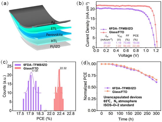
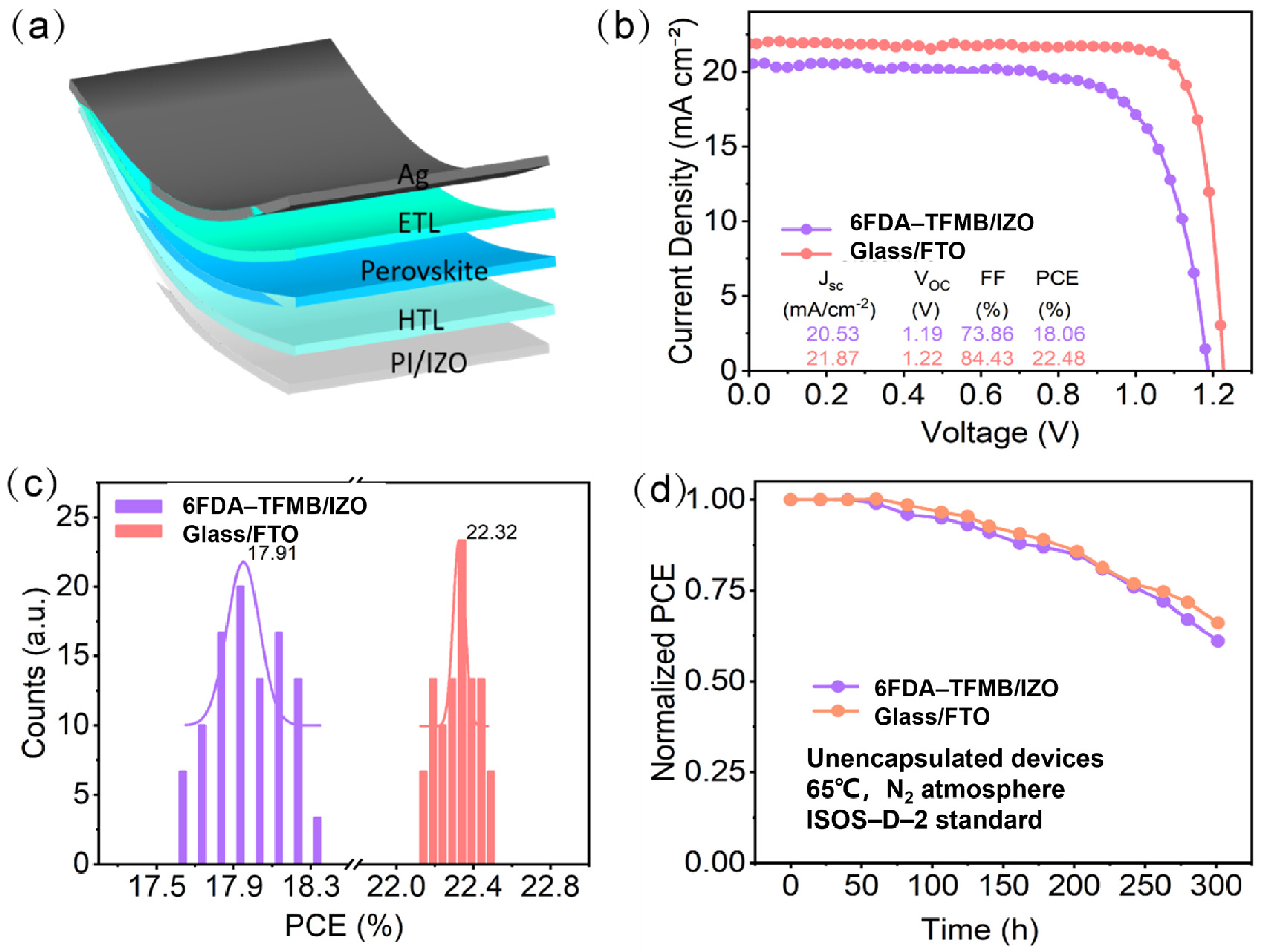
We further fabricated perovskite solar cells on the 6FDA-TFMB/IZO flexible substrate, with the device architecture shown in Figure 2a. As shown in Figure 2b, the resulting flexible device achieves a PCE of 18.06%. Although this value is slightly lower than that of the rigid reference device (Glass/FTO, 22.48%), it remains relatively high among comparable flexible devices, demonstrating the potential of fluorine-containing polyimide films as high-performance flexible substrates. The inset digital photograph shows the device’s excellent bendability, further supporting its application prospects in wearable and portable photovoltaics.
Figure 2.
(a) Schematic illustration of the flexible perovskite solar cell structure. (b) Current density–voltage (J–V) curves of the 6FDA-TFMB/IZO flexible device and the Glass/FTO rigid device, with an inset showing a photograph of the flexible device in a bent state. (c) Statistical distribution of power conversion efficiency (PCE) for the control and target devices. (d) Long-term thermal stability of the devices.
Figure 2c presents the statistical efficiency distribution of 30 devices. The average efficiency of devices based on the 6FDA-TFMB/IZO flexible system reaches 17.91%. The lower absolute efficiency of flexible devices relative to the FTO reference is commonly observed in flexible-cell research and is generally attributed to the higher sheet resistance and surface roughness of flexible substrates. Nevertheless, the narrow Gaussian distribution confirms the good film-forming quality and satisfactory process reproducibility of the developed flexible polyimide substrate and IZO electrode, supporting stable photoelectric conversion output.
Furthermore, Figure 2d shows results from long-term stability tests under a nitrogen atmosphere at 65 °C, and the PCE decay curves of the flexible and rigid devices nearly overlap, indicating comparable thermal-stability performance for both device types. This finding not only verifies the polyimide substrate’s outstanding heat resistance during device fabrication, but also highlights its advantages for flexible photovoltaic devices.
3.5. PI-Assisted SAM Modification of the Buried Interface
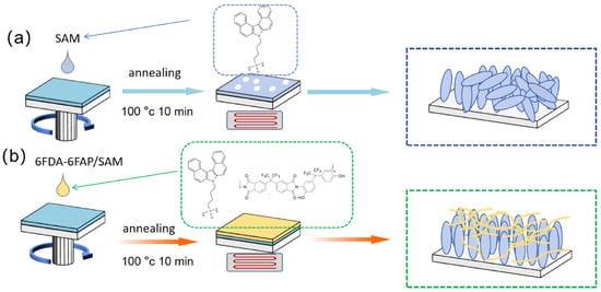
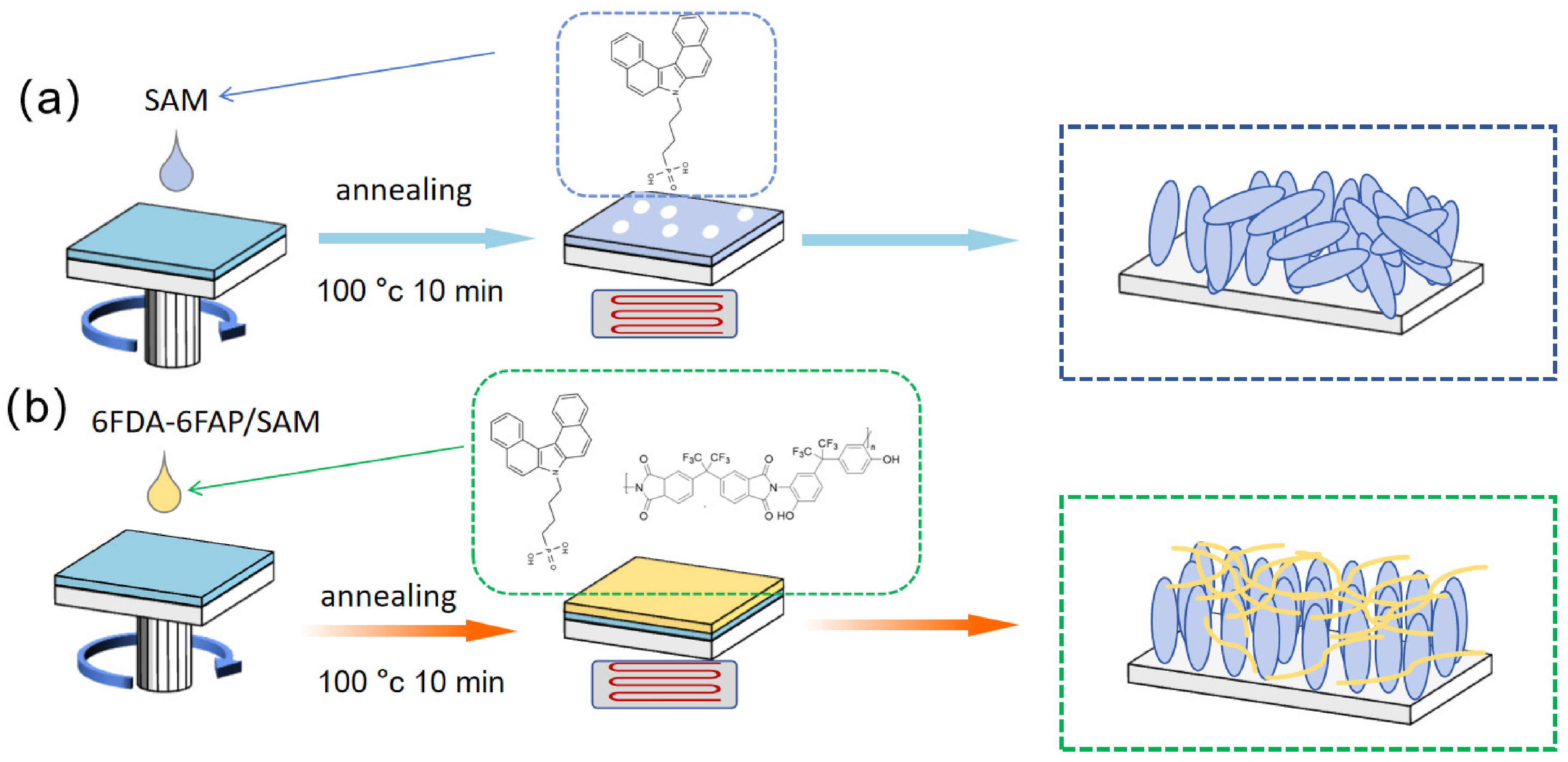
Polyimide materials offer advantages beyond flexible devices. For rigid perovskite solar cells, achieving homogeneous coverage and dense packing of self-assembled monolayers (SAMs) on the substrate surface remains a core challenge for efficient, stable device performance. Accordingly, we introduced 6FDA-6FAP into perovskite solar cell devices to form a mixed hole-transport layer alongside SAMs. 6FDA-6FAP was utilized to disperse 4PADCB and suppress its clustering effect. Meanwhile, the formation of In–O–P bonds strengthens interaction with the ITO substrate, substantially improving SAM coverage and uniformity. To further optimize the interfacial structure, this work adopts a strategy of constructing a composite interfacial layer using polyimide (6FDA-6FAP) and SAMs (4PADCB) (Figure 3).
Figure 3.
Schematic illustration of the polyimide (6FDA-6FAP)-assisted SAM modification strategy: (a) control group (pristine SAMs); (b) target group (6FDA-6FAP/SAM composite).
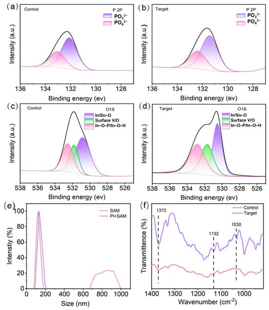
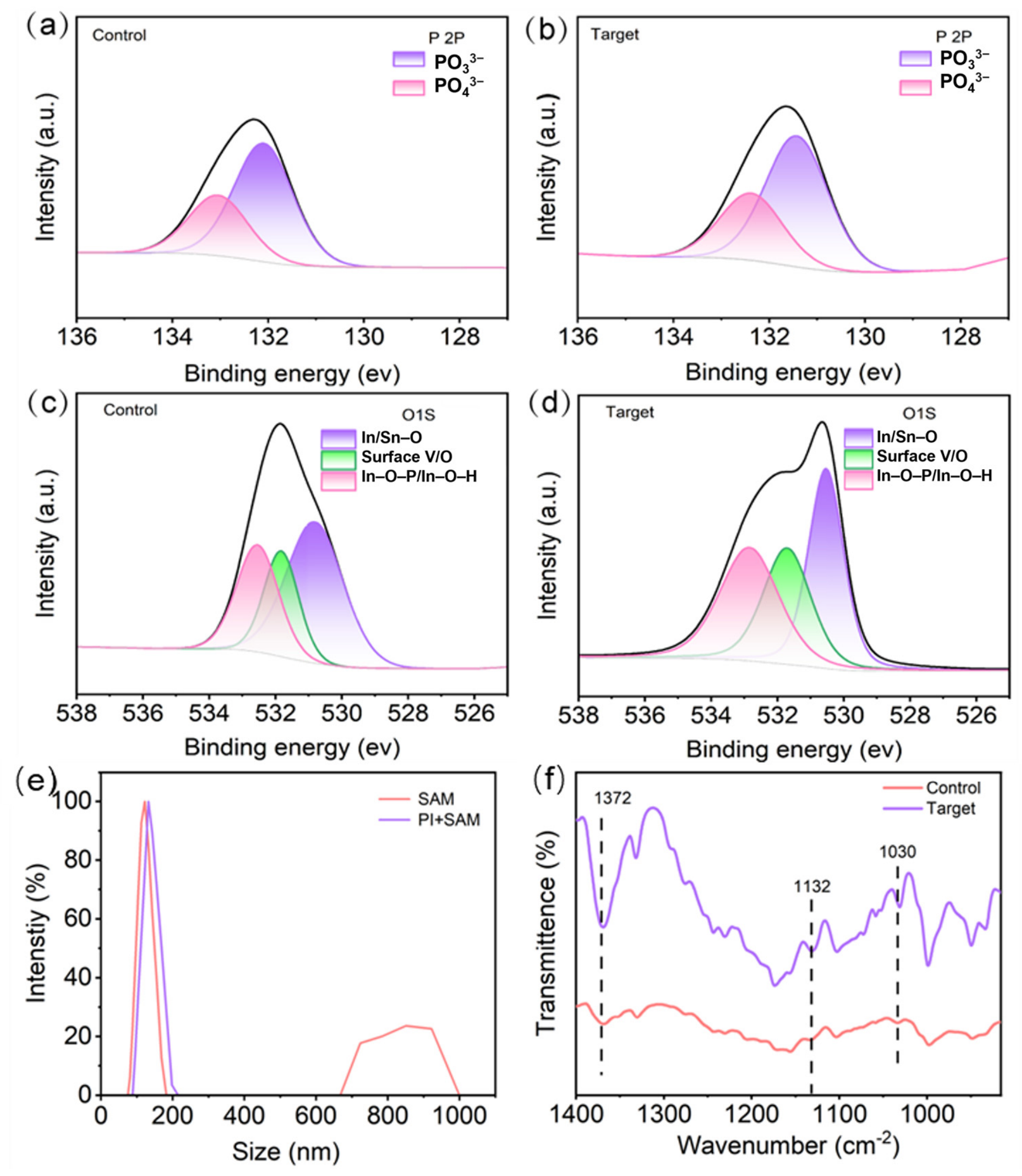
X-ray photoelectron spectroscopy (XPS) was utilized to further investigate the interfacial interaction between the PI layer and the ITO substrate. Figure 4a,b present the high-resolution P 2p spectra of the samples. The results show that the target sample exhibits distinct characteristic peaks near 131 and 132 eV, assigned to the binding-energy signals of phosphite (PO3−4) and phosphate (PO43−) groups, respectively. In the mixed self-assembly system, the phosphorus binding energy shifts to lower values than in the control group. This phenomenon can be ascribed to the anchoring effect of the hydroxyl and carbonyl groups in the 6FAP unit, as well as the strong chemical bonding formed on the surface of the mixed assembled film, which alters the electron-cloud density surrounding the phosphorus atoms. This observation is consistent with the FTIR results [21,44].
Figure 4.
(a,b) P 2p XPS spectra of the control and target SAMs. (c,d) O 1s XPS spectra of the control and target SAMs. (e) Dynamic light scattering (DLS) spectra of SAM and mixed SAM solutions. (f) Fourier transform infrared (FTIR) spectra of SAMs and mixed SAMs.
Figure 4c,d show the deconvoluted O 1s spectra. The fitting integral-area data summarized in Table S6 enable an in-depth analysis of interfacial bonding behavior. The O 1s signal is deconvoluted into three characteristic peaks: interfacial bonded oxygen (In–O–P /In–OH) at 532.83 eV, surface oxygen vacancies (Surface Vo) at 531.73 eV, and lattice oxygen (In/Sn–O) at 530.53 eV. As listed in Table S6, each peak area represents the relative content of the corresponding component. For the target group, the area fraction of the In–O–P/In–OH signal increases significantly from 27.77% (control group) to 34.58%. Given that 6FDA-6FAP contains abundant carbonyl and hydroxyl groups, and the anchoring groups form robust In–O–P chemical bonds with indium atoms on the ITO surface, this increased proportion also provides evidence that the mixed self-assembly system has a high coverage on the ITO substrate and enhances the interfacial interaction [45,46].
Dynamic light scattering (DLS) was employed to characterize the molecular state within the self-assembly precursor solution. As shown in Figure 4e, the pure 4PADCB solution shows a clear bimodal distribution. In addition to the small-molecule peak at 75–183 nm, a prominent aggregation peak appears around 723–922 nm, indicating strong self-aggregation of 4PADCB molecules. After adding 6FDA-6FAP to prepare the mixed solution, the large-size aggregation signal disappears completely, and the spectrum shifts to a uniform unimodal distribution (96–198 nm). This transition provides evidence for strong intermolecular interactions between polyimide chains and 4PADCB molecules. Incorporating PI chains effectively suppresses self-aggregation of small molecules and improves solution stability and dispersibility.
We further acquired FTIR spectra of PI/SAM mixtures for experimental verification. As can be observed in Figure 4f, pure 4PADCB shows three characteristic FTIR peaks originating from carbazole-related vibrations at 1372, 1132, and 1030 cm−1, which are assigned to C–N, P–O, and P–OH stretching vibrations, respectively. Upon mixing with PI, the P–O and P–OH stretching peaks of 4PADCB shift toward lower wavenumbers, confirming interactions between the phosphoric-acid groups of 4PADCB and 6FDA-6FAP. We speculate that this effect may arise from steric hindrance and electrostatic repulsion from the fluorine atoms in 6FDA-6FAP, which hinder SAM agglomeration and further enhance dispersion stability in solution. The excellent homogeneity of the mixed solution provides an experimental foundation for constructing dense, flat mixed self-assembled monolayers on ITO substrates in subsequent procedures [43].
Water contact angle measurements on the ITO/control SAM and ITO/mixed SAM substrates are provided in Figure S10 for reference.
3.6. SAM Coverage and Surface Potential
Cyclic voltammetry (CV) was employed to further verify the coverage of SAMs on ITO substrates and characterize the improvement in self-assembled-film coverage induced by 6FDA-6FAP. As shown in Figure S8, both sample sets exhibit stable redox peaks across scan rates (Figure S8a,b), indicating that introducing 6FDA-6FAP does not hinder interfacial charge transport. The oxidation-peak current (ip,o) of both samples increases linearly with the rising scan rate (v) (Figure S8c,d), revealing that the electrochemical process is governed by surface-adsorption kinetics and further confirming the successful anchoring of active molecules on the ITO surface. According to linear-fitting calculations, the surface coverage of pure SAMs is 8.9 × 10¹³ molecules cm−2. Incorporating 6FDA-6FAP to form mixed SAMs increases surface coverage markedly to 9.72 × 10¹³ molecules cm−2. This coverage enhancement (ca. 9.2%) is attributed to strong intermolecular interactions between polar groups within 6FDA-6FAP and the anchoring molecules, which effectively fill the interstitial voids of pristine single-component SAMs on the ITO substrate and thus construct a more complete and compact self-assembled monolayer, in line with recent strategies that reinforce SAM coverage through polymer-assisted assembly [47]. These results indicate that incorporating 6FDA-6FAP does not impede interfacial charge transport; instead, it improves self-assembled film coverage through void-filling and chain-induced effects.
To further probe the modulation of the self-assembled monolayer surface potential by 6FDA-6FAP, Kelvin probe force microscopy (KPFM) measurements were carried out. KPFM topography and potential maps (Figure S9a,b) show that 6FDA-6FAP modification homogenizes the buried interface (the ITO/SAM or ITO/PI-SAM substrates before perovskite deposition) potential and suppresses carrier accumulation at defect sites. Quantitative statistics (Figure S9c) indicate that the average surface potential of the target sample shifts positively from 190 mV (control) to 341 mV. This positive shift arises from oriented surface dipoles induced by the strongly electronegative –CF3 groups within 6FDA-6FAP, benefiting interfacial charge extraction and transport. Meanwhile, the full width at half maximum (FWHM) of the potential distribution narrows from 65 to 40 mV. This confirms that 6FDA-6FAP fills vacancies and enables cooperative molecular arrangement, forming a more uniform potential interface than single-component SAMs, restraining local non-radiative recombination and supporting improved Voc and FF, consistent with recent hybrid-interface designs for efficient hole extraction [48].
3.7. Effects on Perovskite Crystallization and Film Morphology
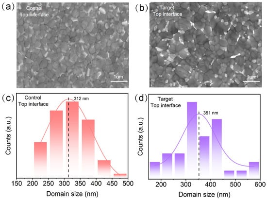
The modified buried interface is expected to improve perovskite absorber-layer growth. Therefore, we used scanning electron microscopy (SEM) to observe the top-surface morphology of perovskite films grown on mixed-SAM-modified substrates. As shown in Figure 5a, perovskite films deposited on single-component-SAM-modified ITO substrates (control) exhibit relatively small grains with dense grain boundaries. Despite full coverage of the film, small grain sizes imply abundant grain boundaries, which generally serve as hot spots for charge recombination and ion migration. Statistical analysis reveals that the average grain size is only approximately 312 nm.
Figure 5.
Top-surface SEM images of the perovskite buried interface for (a) the control group and (b) the mixed target group; (c,d) corresponding grain-size distributions.
In comparison, after modifying the interface with mixed SAMs constructed using 6FDA-6FAP (target, Figure 5b), the grain size of the perovskite film increases substantially. Statistical grain-size analysis (Figure 5c,d) shows that the average grain size in the target group rises above 350 nm; the distribution curve shifts distinctly toward larger values, and more large grains with diameters ranging from 450 to 600 nm are observed. Larger grains correspond to reduced grain-boundary density. Since grain boundaries act as dominant non-radiative recombination centers, fewer grain boundaries can markedly suppress leakage current and consequently elevate the open-circuit voltage (Voc). Further AFM measurements (Figure S11) uncover the micro-scale flatness variation in the films. The root-mean-square (RMS) roughness of the target-group film decreases from 35.81 to 25.68 nm, indicating a smoother and denser surface morphology.
To further explore the effect of 6FDA-6FAP on perovskite-layer crystallization and film formation, we characterized and compared cross-sectional SEM images and XRD patterns of perovskite films with and without polyimide modification. Cross-sectional SEM micrographs (Figure S12a,b) reveal that the modified perovskite film exhibits a prominent, continuous, through-thickness columnar grain structure, directly confirming the optimized vertical crystal orientation. In contrast to the pinhole defects at the buried interface of the control sample, the target group shows a flat, compact interfacial contact with fully developed vertically oriented grains [45]. Combined with the XRD phase analysis in Figure S13 and the SEM characterization in Figure S12, all films display characteristic diffraction peaks of the cubic phase. Upon introducing 6FDA-6FAP, the diffraction intensity of the (001) plane markedly exceeds that of the control group. This demonstrates that the polyimide component effectively improves the ordering of the perovskite lattice arrangement and greatly enhances film crystallinity.
3.8. Interaction Between 6FDA-6FAP and PbI2
Fourier-transform infrared spectroscopy (FTIR) was used to verify the interaction between PI and PbI2. As shown in Figure S14, after mixing 6FDA-6FAP with PbI2, the asymmetric and symmetric imide-ring C=O stretching peaks at approximately 1777 and 1724 cm−1 shift noticeably to lower wavenumbers. Pb2+ coordinates with the oxygen atom of C=O: the strong electron-withdrawing effect of Pb2+ reduces the electron density of the C=O bond. Meanwhile, the 6FDA and 6FAP units contain highly electronegative hexafluoroisopropyl groups, whose fluorine atoms generate strong electrostatic interactions with Pb2+ and induce corresponding shifts of the characteristic C–F vibration peaks. These findings confirm that 6FDA-6FAP binds to under-coordinated Pb2+ on the perovskite surface via multi-site coordination and electrostatic interactions, enabling effective passivation of interfacial defects [49].
3.9. Carrier Transport and Recombination Dynamics
The dynamic balance between interfacial charge extraction and carrier recombination is critical for boosting the optoelectronic performance of perovskite solar cells. To investigate how 6FDA-6FAP modification affects interfacial charge transport kinetics, we characterized PL and TRPL spectra of perovskite films under photoexcitation from the ITO side (Figure S15a). As shown in Figure S15b, all samples exhibit PL emission peaks near 740 nm, corresponding to an optical bandgap of approximately 1.68 eV. The steady-state PL intensity of the 6FDA-6FAP-treated perovskite film decreases drastically compared with the control sample, revealing prominent fluorescence quenching and indicating more efficient charge transfer and hole extraction at the interface. The TRPL decay curves were further fitted using a bi-exponential function (Figure S15c and Table S7). The average carrier lifetime (AVE) of the target film shortens from 695.6 to 672.3 ns. The reduced carrier lifetime, along with the decreased steady-state PL intensity, confirms that introducing 6FDA-6FAP greatly accelerates carrier migration from the perovskite active layer toward the interface [38,50]. This stems from the smoother, denser buried interface after modification, which not only reduces interfacial charge-transport resistance but also suppresses non-radiative recombination losses.
To further explore the influence of interfacial modification on carrier transport and recombination kinetics, transient photocurrent (TPC) and transient photovoltage (TPV) spectra of the devices were characterized (Figure S16). Photocurrent decay correlates with charge extraction and transport processes, while photovoltage decay mainly characterizes charge recombination. As presented in Figure S16a, the voltage decay time of the target sample increases from 3.45 to 4.81 ms. Meanwhile, Figure S16b shows that the transient photocurrent decay time of the target sample shortens markedly from 2.35 to 1.66 μs, demonstrating that the modification layer optimizes the interfacial charge extraction pathway and accelerates the collection of photogenerated carriers, in agreement with recent molecular-bridge designs at SAM–perovskite interfaces [46]. The substantial extension of carrier lifetime confirms that 6FDA-6FAP successfully passivates interfacial defects, effectively suppressing interfacial non-radiative recombination losses. The concurrent improvements in TPC and TPV collectively account for the overall enhancement in the fill factor and open-circuit voltage of the devices.
To further probe interfacial carrier recombination kinetics, we performed electrochemical impedance spectroscopy (EIS) on both device sets. The perovskite solar cell structure was modeled as an equivalent circuit, and Nyquist plots were collected under dark bias. As shown in Figure S17a, the 6FDA-6FAP-modified device shows a larger recombination resistance (Rrec) than the control group, indicating effective suppression of interfacial non-radiative recombination losses, consistent with recent buried-interface engineering strategies [39]. Mott–Schottky plots (Figure S17b) were next used to evaluate the change in built-in potential (Vbi) before and after 6FDA-6FAP modification. The Vbi rises from 1.12 to 1.16 V after incorporating 6FDA-6FAP. The increased Vbi represents better energy-level alignment, more efficient carrier separation and restrained recombination, which is the main contributor to the improved open-circuit voltage (Voc). Furthermore, dark J–V measurements (Figure S17c) were carried out to assess the interfacial defect states. The target device shows a substantially lower dark current density than the control, indicating that 6FDA-6FAP modification suppresses non-radiative carrier recombination and charge leakage, consistent with the EIS results.
3.10. Photovoltaic Performance and Device Stability
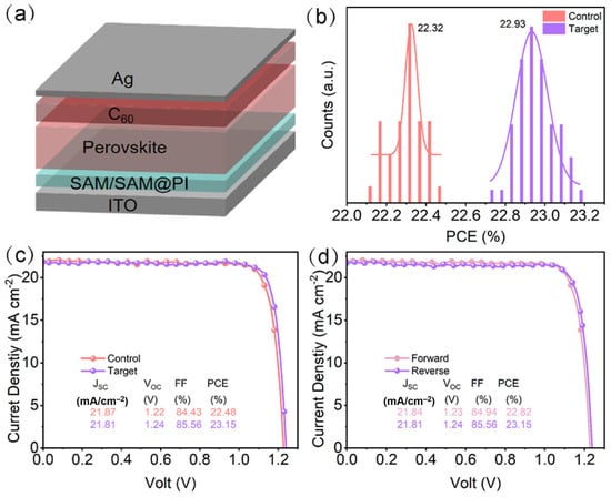
To investigate the effect of the mixed-SAM interfacial layer on the photovoltaic performance of perovskite solar cells (PSCs), inverted (p-i-n) devices with the architecture ITO/SAMs (or PI/SAMs)/perovskite/LiF/C60/BCP/Ag were fabricated in this study, and the schematic diagram is presented in Figure 6a. To evaluate the reproducibility of the performance improvement, the PCE distribution of 30 independent devices was statistically analyzed. As shown in the histogram in Figure 6b, the average PCE of the experimental devices (22.93%) is obviously higher than that of the control group (22.32%). Notably, the efficiency distribution of the experimental devices is much narrower, highlighting the superior film uniformity and process stability enabled by 6FDA-6FAP modification.
Figure 6.
(a) Schematic illustration of the layered structure of the perovskite solar cell (ITO/SAMs (or PI/SAMs)/perovskite/LiF/C60/BCP/Ag); (b) statistical distribution of PCE for the control and target devices; (c) J–V curves of the control and target devices; and (d) J–V curves of the target device under forward and reverse scans.
In this architecture, 6FDA-6FAP acts as a multifunctional interfacial modification layer between the ITO electrode and the perovskite absorber layer. Figure 6c compares the current-density–voltage (J–V) curves of the control and experimental devices. The control device based on pristine SAMs achieves a PCE of 22.48%, with an open-circuit voltage (Voc) of 1.22 V, a short-circuit current density (Jsc) of 21.87 mA cm−2 and a fill factor (FF) of 84.43%. In contrast, the experimental device modified with 6FDA-6FAP delivers a significantly improved PCE of 23.15%, mainly due to simultaneous enhancements in Voc (1.24 V) and FF (85.56%). The increased Voc indicates that introducing 6FDA-6FAP effectively passivates defects at the hole-transport/perovskite interface, suppressing non-radiative recombination losses. Moreover, the experimental device shows negligible hysteresis between forward and reverse scans (Figure 6d), indicating efficient charge extraction and balanced carrier transport after 6FDA-6FAP modification, consistent with recent heterointerface-strengthening designs [51].
External quantum efficiency (EQE) measurements further verify the reliability of the J–V results. As shown in Figure S18a, the experimental device exhibits a high photoresponse exceeding 90% in the visible region (400–750 nm). The integrated Jsc derived from the EQE spectrum is 21.2 mA cm−2, which agrees well with the J–V measured value of 21.8 mA cm−2 (error < 5%), confirming the high reliability of the photovoltaic data. Finally, the normalized EQE and its derivative with respect to photon energy (d(EQE)/dE) in Figure S18b were used to determine the optical bandgap (Eg) of the perovskite film. The peak position of the derivative yields an Eg of 1.68 eV, consistent with the PL results and characteristic of wide-bandgap perovskites suitable for high-efficiency single-junction or tandem solar cells.
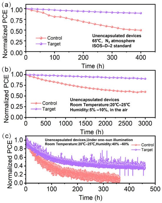
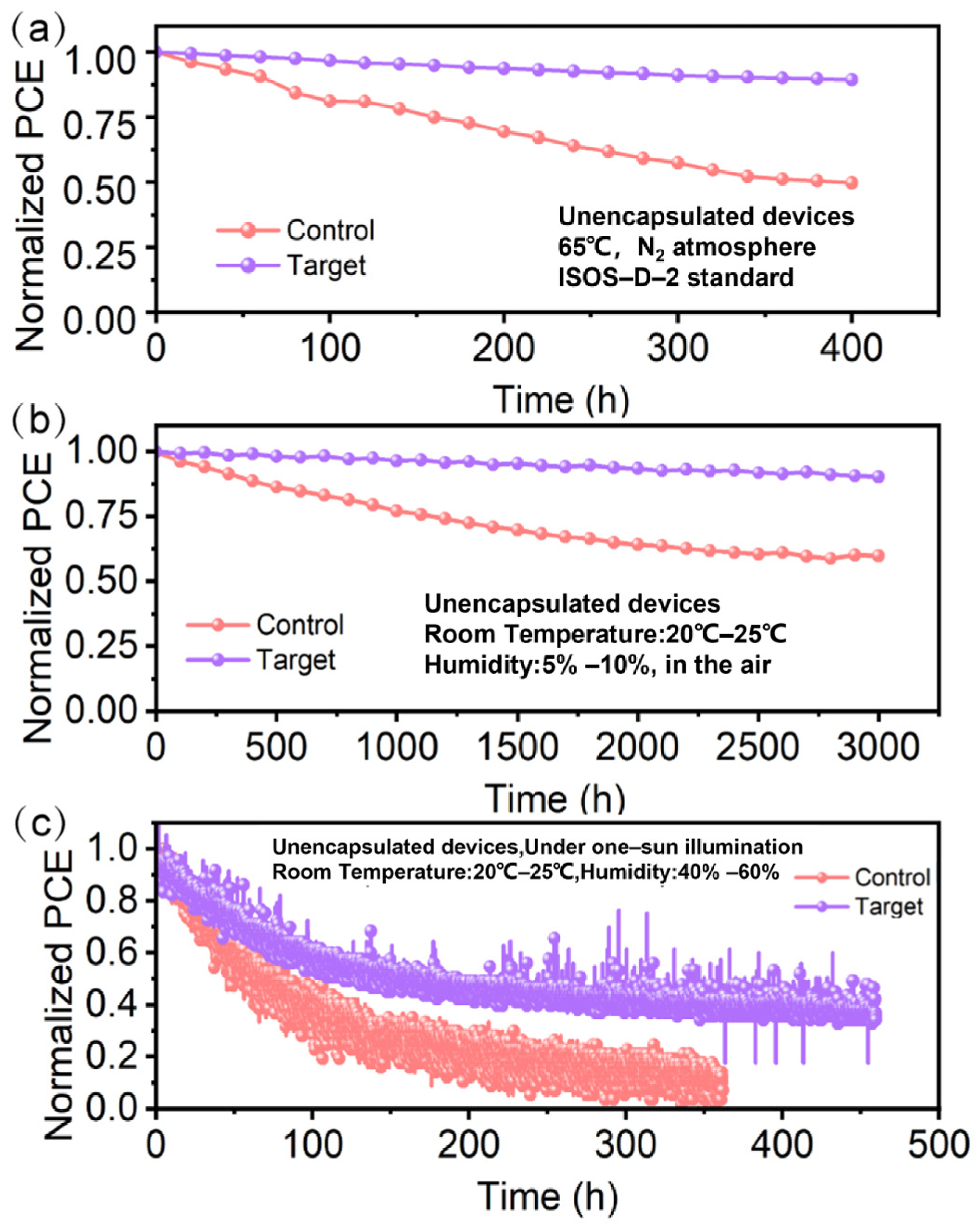
The thermal, ambient, and operational stability of the rigid devices was further evaluated (Figure 7a–c). For thermal stability tests, devices were aged at 65 °C inside a nitrogen-filled glovebox. The control device retains approximately 50% of its initial PCE after 400 h; by contrast, the polyimide-modified device exhibits outstanding thermal stability, maintaining over 90% of its initial efficiency under identical conditions. This confirms that the incorporation of the polyimide layer greatly improves device thermal stability. For ambient stability tests, devices were stored in the dark under room-temperature ambient air for up to 3000 h. The control device’s PCE gradually decays to ~60% of its initial value, while the modified device retains roughly 90% of its initial efficiency after 3000 h, showing superior stability. Furthermore, continuous maximum-power-point tracking tests were carried out to validate operational stability. The control device nearly fails after around 300 h, whereas the polyimide-modified device still preserves ~40% of its initial efficiency over the same timescale. These results are consistent with recent stabilization strategies for SAM-based inverted devices [38].
Figure 7.
(a–c) Stability tests of perovskite solar devices with/without mixed hole-transporting layers of PI and SAMs under different environmental conditions.
4. Conclusions
In summary, three polyimides (6FDA-TFMB, 6FDA-HFPB and 6FDA-6FAP) were rationally designed and synthesized by polymerizing 6FDA with three different diamine monomers. FTIR spectra verified the complete imidization of the poly(amic acid) precursors. GPC results revealed that 6FDA-TFMB possessed the highest molecular weight, which enables the formation of continuous, defect-free thin films. XRD confirmed the amorphous nature of all three polyimides, and 6FDA-TFMB exhibited tighter molecular chain packing than its counterparts. TGA and DSC measurements demonstrated that 6FDA-TFMB possesses the highest decomposition temperature and glass-transition temperature (514.1 and 339.0 °C, respectively) among the three polymers, while UV–vis characterization showed that 6FDA-TFMB has the highest transmittance in the visible range (90.7%). With its high molecular weight, dense chain packing, outstanding thermal resistance, and superior optical transparency, 6FDA-TFMB was successfully used as a flexible substrate for perovskite solar cells. Flexible devices based on IZO/6FDA-TFMB composite conductive substrates achieved a PCE of 18.06%, benefiting from the stable film morphology and favorable interfacial contact. As a reference material, 6FDA-HFPB was only characterized at the material level without device fabrication, owing to its suboptimal overall performance. By comparison, 6FDA-6FAP, with abundant hydroxyl and carbonyl groups, was applied to construct rigid wide-bandgap perovskite devices with mixed PI/SAMs hole-selective layers; the composite interface suppressed SAM aggregation, raised SAM coverage on ITO, optimized perovskite crystallization and passivated buried-interface defects, raising the device PCE from 22.48% to 23.15% with markedly enhanced thermal and environmental stability. This work demonstrates an effective molecular engineering strategy to tailor the chain rigidity, molecular packing, thermal and optical properties of polyimides for targeted flexible-substrate or buried-interface applications in optoelectronic devices. These tunable polyimide materials show strong application prospects in optoelectronics.
Supplementary Materials
The following supporting information can be downloaded at https://www.mdpi.com/article/10.3390/en19215279/s1: Figure S1: Reaction equations for the synthesis of the three polyimides; Figure S2: TGA, DSC and UV–vis characterization of the three polyimide films; Figure S3: 1H NMR spectrum of 6FDA-TFMB; Figure S4: 1H NMR spectrum of 6FDA-HFPB; Figure S5: 1H NMR spectrum of 6FDA-6FAP; Figure S6: DFT-calculated HOMO, LUMO and ESP distributions of the three polyimide repeating units; Figure S7: Optical, mechanical and thermal characterization of the 6FDA-TFMB/IZO composite conductive film; Figure S8: CV characterization of the SAMs and mixed SAMs on ITO; Figure S9: KPFM characterization of the SAMs and mixed SAMs on ITO; Figure S10: Water contact angle measurements of the SAMs and mixed SAMs on ITO; Figure S11: AFM images of the perovskite films; Figure S12: Cross-sectional SEM images of the perovskite films; Figure S13: XRD patterns of the perovskite films; Figure S14: FTIR spectra of 6FDA-6FAP with and without PbI2; Figure S15: PL and TRPL characterization of the perovskite films; Figure S16: TPC and TPV decay curves of the devices; Figure S17: EIS, Mott–Schottky and dark J–V characterization of the devices; Figure S18: EQE characterization of the target device; Table S1: GPC data of the three polyimides; Table S2: XRD peak positions and d-spacings of the polyimides; Table S3: Thermal properties of the three polyimide films; Table S4: Optical performance parameters of the three polyimides; Table S5: DFT-calculated orbital energies and band gaps; Table S6: Fitted integral areas of the O 1s XPS spectra; Table S7: TRPL fitting parameters of the devices.
Author Contributions
Conceptualization, M.H. and P.G.; methodology, M.H. and C.L.; validation, S.L., Y.C. and Z.T.; Writing—original draft, S.L.; Writing—review and editing, S.L.; Supervision, P.G.; Funding acquisition, P.G. All authors have read and agreed to the published version of the manuscript.
Funding
This research was funded by the National Natural Science Foundation of China (Grant nos. 22575246); State Key Laboratory of Structural Chemistry (Grant nos. 20255101); the Fujian Provincial Key Science and Technology Program (No. 2025HZ028025).
Data Availability Statement
The data presented in this study are available on request from the corresponding author.
Conflicts of Interest
The authors declare no conflicts of interest.
References
- Lee, S.; Bae, S.; Kim, D.; Lee, H. Historical Analysis of High-Efficiency, Large-Area Solar Cells: Toward Upscaling of Perovskite Solar Cells. Adv. Mater. 2020, 32, 2002202. [Google Scholar] [CrossRef] [Scilit] [PubMed]
- Shimpi, T.M.; Drayton, J.; Swanson, D.E.; Sampath, W.S. Properties of Nitrogen-Doped Zinc Telluride Films for Back Contact to Cadmium Telluride Photovoltaics. J. Electron. Mater. 2017, 46, 5112–5120. [Google Scholar] [CrossRef] [Scilit]
- Liu, F.-W.; Cheng, T.-M.; Chen, Y.-J.; Yueh, K.-C.; Tang, S.-Y.; Wang, K.; Wu, C.-L.; Tsai, H.-S.; Yu, Y.-J.; Lai, C.-H.; et al. High-Yield Recycling and Recovery of Copper, Indium, and Gallium from Waste Copper Indium Gallium Selenide Thin-Film Solar Panels. Sol. Energy Mater. Sol. Cells 2022, 241, 111691. [Google Scholar] [CrossRef] [Scilit]
- Gao, S.; Fan, X.; Wang, J.; Wei, F.; Chen, J.; Liu, X.; Wang, J.; Huang, H.; Li, J.; Zhang, Z.; et al. Over 26% and 24%-Efficiency Rigid and Flexible Perovskite Photovoltaics through Enhanced Crystallinity and Alleviated Residual Strains. ACS Nano 2025, 19, 28888–28899. [Google Scholar] [CrossRef] [Scilit] [PubMed]
- Green, M.A.; Dunlop, E.D.; Yoshita, M.; Kopidakis, N.; Bothe, K.; Siefer, G.; Hao, X.; Jiang, J.Y. Solar Cell Efficiency Tables (Version 66). Prog. Photovolt. Res. Appl. 2025, 33, 795–810. [Google Scholar] [CrossRef] [Scilit]
- Yin, S.; Luo, X.; Tang, F.; Xiong, Z.; Lin, Y.; Yang, W.; Shu, Y.; Wang, Y.; Ying, L. A Green-Solvent-Processable Polymer Hole Transport Material for Achieving 26.31% Efficiency in Inverted Perovskite Solar Cells. Energy Environ. Sci. 2025, 18, 4153–4161. [Google Scholar] [CrossRef] [Scilit]
- Wang, X.; Ling, Y.; Chiu, Y.-C.; Du, Y.; Barreda, J.L.; Perez-Orive, F.; Ma, B.; Xiong, P.; Gao, H. Dynamic Electronic Junctions in Organic–Inorganic Hybrid Perovskites. Nano Lett. 2017, 17, 4831–4839. [Google Scholar] [CrossRef] [Scilit] [PubMed]
- Arciniegas, M.P.; Manna, L. Designing Ruddlesden–Popper Layered Perovskites through Their Organic Cations. ACS Energy Lett. 2022, 7, 2944–2953. [Google Scholar] [CrossRef] [Scilit]
- Krückemeier, L.; Krogmeier, B.; Liu, Z.; Rau, U.; Kirchartz, T. Understanding Transient Photoluminescence in Halide Perovskite Layer Stacks and Solar Cells. Adv. Energy Mater. 2021, 11, 2003489. [Google Scholar] [CrossRef] [Scilit]
- Hassan, A.; Syauqi, M.I.; Liu, Y.; Ke, Z.; Lin, W.; Wang, Z.; Jin, Y.; Azmi, R. Unveiling the Potential of Flexible Perovskite Photovoltaics: From Lab to Fab. Mater. Sci. Eng. R Rep. 2025, 166, 101023. [Google Scholar] [CrossRef] [Scilit]
- Sava, I.; Damaceanu, M.-D.; Constantin, C.-P.; Asandulesa, M.; Wolińska-Grabczyk, A.; Jankowski, A. Structure–Promoted High Performance Properties of Triphenylmethane-Containing Polyimides and Copolyimides. Eur. Polym. J. 2018, 108, 554–569. [Google Scholar] [CrossRef] [Scilit]
- Mushtaq, N.; Zhang, Y.; Nazir, M.; Tan, L.; Chen, G.; Fang, X. Ultra-High Tg Colorless Polyimide Film with Balanced Optical Retardation and Coefficient of Thermal Expansion for Flexible Display. Polymer 2025, 321, 128085. [Google Scholar] [CrossRef] [Scilit]
- Wang, C.; Cao, S.; Chen, W.; Xu, C.; Zhao, X.; Li, J.; Ren, Q. Synthesis and Properties of Fluorinated Polyimides with Multi-Bulky Pendant Groups. RSC Adv. 2017, 7, 26420–26427. [Google Scholar] [CrossRef] [Scilit]
- Li, F.; Liu, J.; Liu, X.; Wang, Y.; Gao, X.; Meng, X.; Tu, G. High Performance Soluble Polyimides from Ladder-Type Fluorinated Dianhydride with Polymorphism. Polymers 2018, 10, 546. [Google Scholar] [CrossRef] [Scilit] [PubMed]
- Feng, J.; Wang, Y.; Qin, X.; Lv, Y.; Huang, Y.; Yang, Q.; Li, G.; Kong, M. Revealing Molecular Mechanisms of Colorless Transparent Polyimide Films under Photo-Oxidation. Polym. Degrad. Stab. 2023, 210, 110294. [Google Scholar] [CrossRef] [Scilit]
- Zhang, T.; Yang, Z.; Piao, F.; Guo, H. Transparent Polyimide Films with Ultra-Low Coefficient of Thermal Expansion. High Perform. Polym. 2022, 34, 871–879. [Google Scholar] [CrossRef] [Scilit]
- Qiao, S.; Kang, S.; Hu, Z.; Yu, J.; Wang, Y.; Zhu, J. Moisture-Resistance, Mechanical and Thermal Properties of Polyimide Aerogels. J. Porous Mater. 2020, 27, 237–247. [Google Scholar] [CrossRef] [Scilit]
- Zheng, S.; Jiang, L.; Chang, F.; Zhang, C.; Ma, N.; Liu, X. Mechanically Strong and Thermally Stable Chemical Cross-Linked Polyimide Aerogels for Thermal Insulator. ACS Appl. Mater. Interfaces 2022, 14, 50129–50141. [Google Scholar] [CrossRef] [Scilit] [PubMed]
- Grabowska, A.; Fuentes Pineda, R.; Spinelli, P.; Pérez, G.S.; Pacheco, F.A.V.; Babu, V. Development of Lightweight and Flexible Perovskite Solar Cells on Ultrathin Colorless Polyimide Foils. ACS Appl. Mater. Interfaces 2024, 16, 48676–48684. [Google Scholar] [CrossRef] [Scilit] [PubMed]
- Zhang, Y.; Chen, Y.; Xiao, X.; Xu, Y.; Xue, S. SnO2/Silver Nanowire/Polyimide Flexible Transparent Conductive Films for Double-Sided Perovskite Solar Cells and Heaters. ACS Appl. Nano Mater. 2024, 7, 20745–20754. [Google Scholar] [CrossRef] [Scilit]
- Yu, Y.-Y.; Tseng, C.; Chien, W.-C.; Hsu, H.-L.; Chen, C.-P. Photovoltaic Performance Enhancement of Perovskite Solar Cells Using Polyimide and Polyamic Acid as Additives. J. Phys. Chem. C 2019, 123, 23826–23833. [Google Scholar] [CrossRef] [Scilit]
- Ma, J.; Fan, S.; Shao, C.; Wang, L.; Dong, Y.; Niu, G.; Nie, Z.; Yang, S.; Wang, J.; Yang, H. Double-Chain Copolymer Network via In Situ Polymerization Enables High-Stability and Lead-Safe Perovskite Solar Cells. Angew. Chem. Int. Ed. 2025, 64, e202425578. [Google Scholar] [CrossRef] [Scilit] [PubMed]
- Liu, C.; Yu, W.; Li, Y.; Wang, C.; Zhang, Z.; Li, C.; Liang, L.; Chen, K.; Liu, L.; Li, T.; et al. Fluorinated Polyimide Tunneling Layer for Efficient and Stable Perovskite Photovoltaics. Angew. Chem. Int. Ed. 2024, 63, e202402904. [Google Scholar] [CrossRef] [Scilit] [PubMed]
- Lee, K.; Choi, J.-M.; Lee, J.; Han, J.; Choi, S.H.; Kotora, M.; Lee, Y.S.; Kim, U.; Won, J.C.; Park, S.; et al. Ultra-Thin Polyimide-Embedded Carbon Nanotube-Based Transparent Conductor and Its Application to Foldable Perovskite Solar Cells. Small Struct. 2026, 7, e70585. [Google Scholar] [CrossRef] [Scilit]
- Kim, J.-W.; Kim, S.; Lee, N.-K.; Cho, H.; Park, S.J.; Kim, J.; Lee, N.; Kim, S.; Cho, S.H.; Lee, S. Ultraviolet-Resistant Flexible Perovskite Solar Cells with Enhanced Efficiency through Attachable Nanophotonic Downshifting and Light Trapping. Small 2025, 21, 2501374. [Google Scholar] [CrossRef] [Scilit] [PubMed]
- Magomedov, A.; Al-Ashouri, A.; Kasparavičius, E.; Strazdaite, S.; Niaura, G.; Jošt, M.; Malinauskas, T.; Albrecht, S.; Getautis, V. Self-Assembled Hole Transporting Monolayer for Highly Efficient Perovskite Solar Cells. Adv. Energy Mater. 2018, 8, 1801892. [Google Scholar] [CrossRef] [Scilit]
- Chu, L.; Ding, L. Self-Assembled Monolayers in Perovskite Solar Cells. J. Semicond. 2021, 42, 090202. [Google Scholar] [CrossRef] [Scilit]
- Fu, Q.; Ji, X.; Tian, S.; Jiang, B.; Tao, L.; Bi, L.; Lu, L.; Dyson, P.J.; Ding, Y.; Nazeeruddin, M.K.; et al. Versatile Self-Assembled Monolayers for Perovskite-Based Optoelectronic Devices. Mater. Today 2025, 89, 192–205. [Google Scholar] [CrossRef] [Scilit]
- Phung, N.; Verheijen, M.; Todinova, A.; Datta, K.; Verhage, M.; Al-Ashouri, A.; Köbler, H.; Li, X.; Abate, A.; Albrecht, S.; et al. Enhanced Self-Assembled Monolayer Surface Coverage by ALD NiO in p-i-n Perovskite Solar Cells. ACS Appl. Mater. Interfaces 2022, 14, 2166–2176. [Google Scholar] [CrossRef] [Scilit] [PubMed]
- Ou, Y.; Huang, H.; Shi, H.; Li, Z.; Chen, Z.; Mateen, M.; Lu, Z.; Chi, D.; Huang, S. Collaborative Interfacial Modification and Surficial Passivation for High-Efficiency MA-Free Wide-Bandgap Perovskite Solar Cells. Chem. Eng. J. 2023, 469, 143860. [Google Scholar] [CrossRef] [Scilit]
- Chiang, Y.-H.; Frohna, K.; Salway, H.; Abfalterer, A.; Pan, L.; Roose, B.; Anaya, M.; Stranks, S.D. Vacuum-Deposited Wide-Bandgap Perovskite for All-Perovskite Tandem Solar Cells. ACS Energy Lett. 2023, 8, 2728–2737. [Google Scholar] [CrossRef] [Scilit] [PubMed]
- Deng, X.; Qi, F.; Li, F.; Wu, S.; Lin, F.R.; Zhang, Z.; Guan, Z.; Yang, Z.; Lee, C.; Jen, A.K. Co-Assembled Monolayers as Hole-Selective Contact for High-Performance Inverted Perovskite Solar Cells with Optimized Recombination Loss and Long-Term Stability. Angew. Chem. Int. Ed. 2022, 61, e202203088. [Google Scholar] [CrossRef] [Scilit] [PubMed]
- Zhang, Z.; Chen, S.; Peng, C.; Xu, Y.; Wang, S.; Li, W.; Zheng, Y.; Wang, W.; Du, S.; Zhou, F.; et al. Amine-Rich Cross-Linking Templates Enabling Toughened Self-Assembled Monolayer for Stable Perovskite Solar Modules. Sci. Adv. 2026, 12, eaeg3206. [Google Scholar] [CrossRef] [Scilit] [PubMed]
- Tang, Q.; Liu, H.; Ding, J.; Zhang, Z.; Lin, W.; Liu, Z.; Deng, Z.; Chen, T.; Li, G.; Song, J.; et al. Buried-Interface Homogenization by Asymmetric Polymeric Self-Assembled Layers Powers Efficient, Durable Flexible Perovskite Photovoltaics. Nat. Commun. 2026, 17, 7039. [Google Scholar] [CrossRef] [Scilit] [PubMed]
- Zhang, H.; Yang, Y.; Zhao, J.; Yang, H.; Lu, Y.; Xie, Y.; Yao, S.; Chu, Z.; Huang, C.; Huang, Z.; et al. A Self-Assembling Composite Structural Design for the Conversion of Hydroxyl-Anchored Bonds Obtains High Efficient and Stable Perovskite Solar Cells. Adv. Mater. 2025, 37, 2420155. [Google Scholar] [CrossRef] [Scilit] [PubMed]
- Liu, W.; Zang, Y.; Tu, Y.; Wang, Y.; Zhu, Z.; Zhu, C.; Yan, W. Reconstruction of Hole Transport Layer via Co-Self-Assembled Molecules for High-Performance Inverted Perovskite Solar Cells. Small 2025, 21, 2408314. [Google Scholar] [CrossRef] [Scilit] [PubMed]
- Zhang, X.; Wang, Y.; Zhang, K.; Tao, M.; Guo, H.; Guo, L.; Song, Z.; Wen, J.; Yang, Y.; Hou, Y.; et al. Reinforcing Coverage of Self-Assembled Monomolecular Layers for Inverted Perovskite Solar Cells with Efficiency of 25.70%. Angew. Chem. Int. Ed. 2025, 64, e202423827. [Google Scholar] [CrossRef] [Scilit] [PubMed]
- Yu, X.; Sun, X.; Zhu, Z.; Li, Z. Stabilization Strategies of Buried Interface for Efficient SAM-Based Inverted Perovskite Solar Cells. Angew. Chem. Int. Ed. 2025, 64, e202419608. [Google Scholar] [CrossRef] [Scilit] [PubMed]
- Xu, R.; Wang, C.; Zhang, Z.; Li, J.; Wei, Y.; Wang, K.; Xiao, M. Buried Interface Engineering: A Key to Unlocking the Potential of Self-Assembled Monolayer (SAM)-Based Inverted Perovskite Solar Cells. Small 2025, 21, 2503114. [Google Scholar] [CrossRef] [Scilit] [PubMed]
- Ma, H.; Li, X.; Li, H.; Guan, J.; Zheng, L.; Wu, J.; He, Z.; Yu, Y.; Wang, J.; Yang, J.; et al. Cation–Anion Synergy Enables Uniform and Stable SAMs for High-Efficiency Perovskite/TOPCon Tandem Solar Cells. Adv. Sci. 2026, 13, e20822. [Google Scholar] [CrossRef] [Scilit] [PubMed]
- Liang, L.; Zhu, W.; Wang, Z.; Chai, W.; Zhang, T.; Xi, H.; Li, Z.; Dong, H.; Zhang, Z.; Sun, L.; et al. Guanidyl-Engineered SAMs with Electrostatic–Coordination Synergy for High-Efficiency Tandem-Compatible Perovskite Solar Cells. Adv. Mater. 2026, 38, e19563. [Google Scholar] [CrossRef] [Scilit] [PubMed]
- Inoue, H.; Sasaki, Y.; Ogawa, T. Comparison of One-Pot and Two-Step Polymerization of Polyimide from BPDA/ODA. J. Appl. Polym. Sci. 1996, 60, 123–131. [Google Scholar] [CrossRef] [Scilit]
- Härtel, M.; Li, B.; Mariotti, S.; Wagner, P.; Ruske, F.; Albrecht, S.; Szyszka, B. Reducing Sputter Damage-Induced Recombination Losses during Deposition of the Transparent Front-Electrode for Monolithic Perovskite/Silicon Tandem Solar Cells. Sol. Energy Mater. Sol. Cells 2023, 252, 112180. [Google Scholar] [CrossRef] [Scilit]
- Huang, L.; Wang, K.-L.; Chen, Z.; Su, Z.-H.; Murodzoda, S.; Chen, X.; Chen, J.; Chen, C.-H.; Xia, Y.; Yang, Y.-T.; et al. SAM molecular stacking with heterogeneous orientation for high-performance perovskite photovoltaics. Chem 2026, 12, 102941. [Google Scholar] [CrossRef] [Scilit]
- Chen, X.; Chen, C.; Su, Z.H.; Chen, J.; Wang, K.; Xia, Y.; Nizamani, N.; Huang, L.; Jin, R.; Li, Y.; et al. Adhesively Bridging SAM Molecules and Perovskites for Highly Efficient Photovoltaics. Adv. Funct. Mater. 2025, 35, 2415004. [Google Scholar] [CrossRef] [Scilit]
- Chen, C.; Liu, G.; Chen, X.; Deger, C.; Jin, R.; Wang, K.; Chen, J.; Xia, Y.; Huang, L.; Yavuz, I.; et al. Methylthio Substituent in SAM Constructing Regulatory Bridge with Photovoltaic Perovskites. Angew. Chem. Int. Ed. 2025, 64, e202419375. [Google Scholar] [CrossRef] [Scilit] [PubMed]
- Ling, H.; Chen, K.; Li, S.; Duan, W.; Li, D.; Liu, C.; Zeng, L.; Liu, T.; Liu, T.; Hu, X.; et al. In Situ Crosslinked Phosphonic Acid Self-Assembled Monolayers toward Efficient and Stable Inverted Perovskite Solar Cells. Adv. Funct. Mater. 2025, 35, 2501563. [Google Scholar] [CrossRef] [Scilit]
- Zheng, C.; Dong, W.; Liu, J.; Zhu, W.; Lv, W.; Zhang, Y.; Li, P.; Xu, L.; Li, M.; Chen, R. Polycarbazole–SAM Hybrid Interface Engineering for Efficient Hole Extraction in Perovskite Photovoltaic Devices. J. Phys. Chem. Lett. 2025, 16, 13223–13230. [Google Scholar] [CrossRef] [Scilit] [PubMed]
- Jiang, X.; Zhang, B.; Yang, G.; Zhou, Z.; Guo, X.; Zhang, F.; Yu, S.; Liu, S.; Pang, S. Molecular Dipole Engineering of Carbonyl Additives for Efficient and Stable Perovskite Solar Cells. Angew. Chem. Int. Ed. 2023, 62, e202302462. [Google Scholar] [CrossRef] [Scilit] [PubMed]
- Zhuang, R.; Sun, A.; Tian, C.; Chen, C.; Liu, S.; Wu, X.; Han, S.; Cai, L.; Chen, J.; Chen, Q.; et al. Co-deposited inverted perovskite photovoltaics towards 27% efficiency via vertical redistribution of self-assembled-molecules and in-situ crosslinking. Nat. Commun. 2026, 17, 5428. [Google Scholar] [CrossRef] [Scilit] [PubMed]
- Peng, C.; Sun, X.; Zhang, B.; Meng, H.; Wang, K.; Li, Z.; Zhu, M.; Zhang, X.; Wang, G.; Zhou, Z.; et al. Strengthened Perovskite/SAM Heterointerface for Stable Perovskite Solar Cells. J. Am. Chem. Soc. 2025, 147, 48391–48399. [Google Scholar] [CrossRef] [Scilit] [PubMed]
Disclaimer/Publisher’s Note: The statements, opinions and data contained in all publications are solely those of the individual author(s) and contributor(s) and not of MDPI and/or the editor(s). MDPI and/or the editor(s) disclaim responsibility for any injury to people or property resulting from any ideas, methods, instructions or products referred to in the content. |
© 2026 by the authors. Licensee MDPI, Basel, Switzerland. This article is an open access article distributed under the terms and conditions of the Creative Commons Attribution (CC BY) license.