


Abstract
This paper proposes a dynamic voltage restorer (DVR) based on a new three-phase multilevel inverter (MLI). An integral component of DVRs is the power electronic converter. At medium-to-high voltage levels, MLIs are the ideal converters for DVR applications because lower voltage-rated switches are used to generate high voltages, thus minimizing power losses. The proposed three-phase MLI generates 15 levels of load voltage per phase, using a reduced component count: eight lower-rated semiconductor power switches, four primary DC voltage sources, two auxiliary DC sources, and eight driver circuits per phase. Additionally, each phase features a low-frequency transformer with voltage-boosting and galvanic isolation capabilities. The switching sequence of the proposed MLI is simpler to execute using fundamental frequency control; this methodology provides reduced switching stress and reduced switching losses as merits. Structurally, the proposed MLI is less complex and thus scalable. The proposed DVR, based on three-phase MLI, efficiently offsets power quality problems such as voltage swell, voltage sags, and harmonics for balanced and unbalanced loads. The operational performance of the proposed DVR-MLI is verified by a simulation, using PSCAD software and an experimental prototype.
1. Introduction
Voltage disturbances such as unbalances, voltage dips, harmonics, flickers, and voltage swell are the commonly faced power quality (PQ) drawbacks in distribution lines [1]. When these voltage disturbances are not satisfactorily resolved, they cause the breakdown of sensitive and critical loads [2]; also, they interfere and cause interruption of production lines, culminating in the loss of essential information and finances [3]. The application of sensitive loads and devices liable for the pollution of power lines has increased in recent times, hence the urgent need for the protection of power systems. Considering IEEE 1159 and 1346 standards, if the nominal voltage of a distribution line decreases from 10% to 90% for a duration lasting between half of a cycle and 60 s, then this phenomenon is described as a voltage dip [4,5]. Some of the causes of voltage dip are short circuit faults, the starting of induction motors with high ratings, and the immediate connection of large loads [6]. The voltage swell phenomenon is described as an increase in the nominal voltage of a power line from 110% to 180% for a duration lasting no more than the frequency of the utility, from half a cycle to 60 s. Some causes of voltage swell are de-energizing large capacitor banks, switching off large capacitors, and the disconnection of large inductive loads. The consequence of voltage swell is the malfunction of industrial devices, due to overheating and tripping of AC motors, relays, and surge arresters [7,8]. Sensitive loads dislike power lines that are heavily contaminated by harmonics because the control of these devices depends largely on the zero crossing and peak value of the input voltage. Different solutions have been proposed to mitigate the consequences of power quality issues on sensitive loads over the years. Among the many presented solutions, custom power devices (CPD) are the most preferred solutions because of their essential attributes, such as flexibility, fast response, and effectiveness.
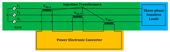
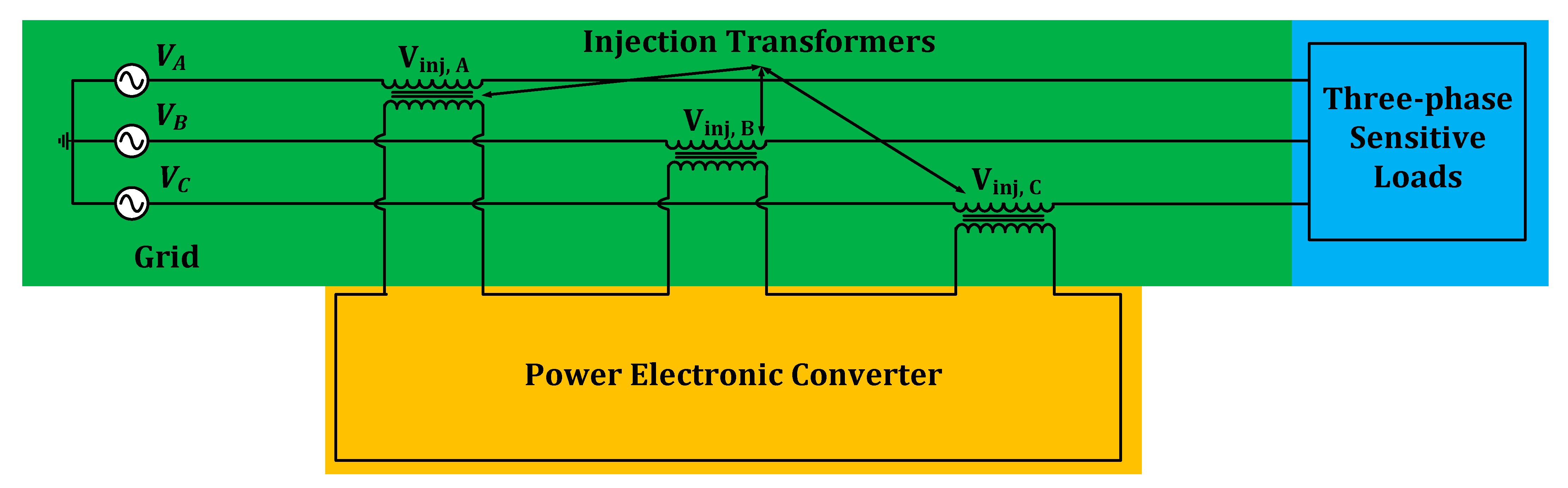
CPDs are new technologies designed to mitigate power quality issues. They are developed upon the concept of power electronics; therefore, they are commonly referred to as power electronic-based compensators. Conventionally, CPDs are categorized into three static distinct groups: (a) series compensator, (b) shunt compensator, and (c) series-shunt compensator. Examples of each of the three static compensators are DVR, DATCOM, and UPQC, respectively. The series compensators comprising SSC (static series compensators), DVC (dynamic voltage compensators), and DVR (dynamic voltage restorers) are regarded as the ideal cost-effective method of damping power quality issues. These compensator families are alike in operating principles and the structure of power circuits but differ in control techniques and design purposes. Examples of other power quality mitigating devices are flywheels, UPS (uninterruptible power supply), tap-changing transformers, and STATCOM (static compensators) [9]. DVR’s functionality is maintaining load voltage at the desired characteristic by injecting voltage with a specific magnitude, phase, and frequency into the distribution line. DVRs are series-tied to the distribution line and have the potential to absorb or generate reactive and real powers [10]. Figure 1 shows the structure of a typical DVR, which consists of the grid, an injection transformer at the point of common coupling (PCC), a voltage source converter, and sensitive loads. The first practical operating DVR is situated in the USA, North Carolina, in a rug-producing company [11]. DVRs are classified into two categories, considering ESS. These are ESS-based DVRs and non-ESS-based DVRs [12]. Previously, EES-based DVRs were unable to compensate for huge and longer periods of voltage interruptions. However, with increased capacity, reduced cost, and increased application of renewable energy sources, ESS-based DVRs are the preferred option for longer and deeper voltage compensations.
Figure 1.
A typical DVR structure.
Non-ESS-based DVRs possess the following merits: reduced system size, minimum system cost because of the absence of ESS, single-stage power conversion, and longer and deeper voltage compensation capabilities. Also, DVRs are classified according to the type of power conversion, i.e., ac-ac DVR, ac-dc-ac DVR, and dc-ac DVR. Each of these topologies of DVR has advantages and disadvantages. The ac-ac topology does not require ESS and is a single-stage power converter, while the ac-dc-ac topology requires bulky capacitors and is a multi-stage power converter. Finally, DVRs are further classified into single-phase and three-phase systems [13,14,15].
The most frequently used converter topologies for both single-phase and three-phase DVRs are full and half H-bridges, matrix converters, multilevel inverters, Z-source inverters, 2-level six-switch inverters, four-leg inverters, and 3 H-bridge inverters [16,17,18,19]. Application of a multilevel inverter in DVRs is the optimal choice when juxtaposed with other inverter topologies: mostly the conventional 2-level inverter, which requires a higher switching frequency, thus increasing switching losses, a higher THD (total harmonic content), and the burden of controller computation [20]. However, a multilevel inverter provides the following advantages: high output voltage using smaller input voltage, high-quality output waveforms, lower THD, reduced switching losses, and better electromagnetic adaptability.
A three-phase seven-level inverter-based dynamic voltage restorer (DVR) is suggested in this paper. The proposed three-phase MLI is composed of a smaller number of circuit components (power switches, DC sources, and driver circuit) but generates high levels of output voltage. This is evident from the comparative perusal of the proposed topology and other published multilevel inverter topologies with similar characteristics. The proposed DVR, based on the new three-phase MLI, is operated under various voltage sag and swell conditions and unbalanced voltage conditions. Experimental and simulation outcomes are presented to affirm the operations of the proposed DVR, based on three-phase MLI.
2. Proposed Three-Phase MLI
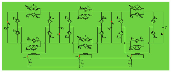
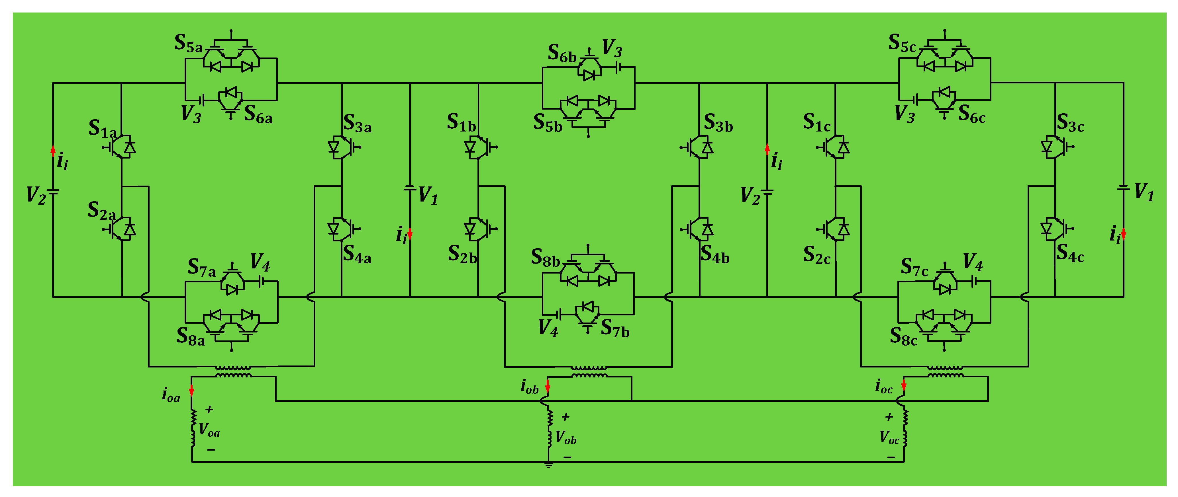
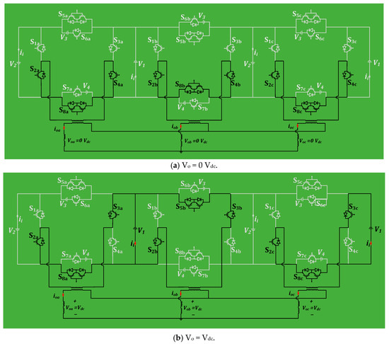
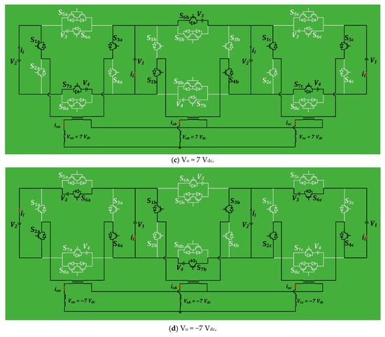
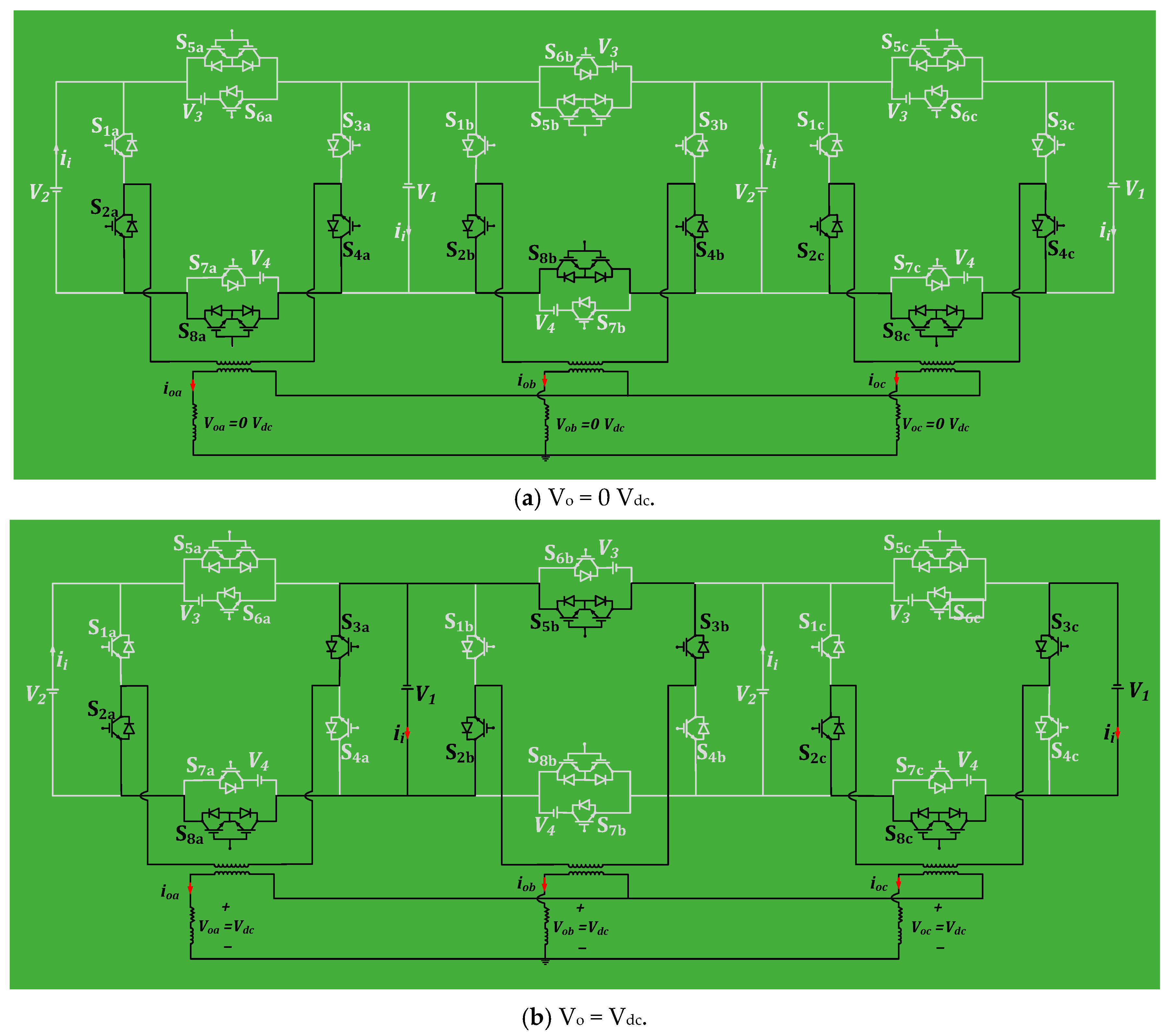
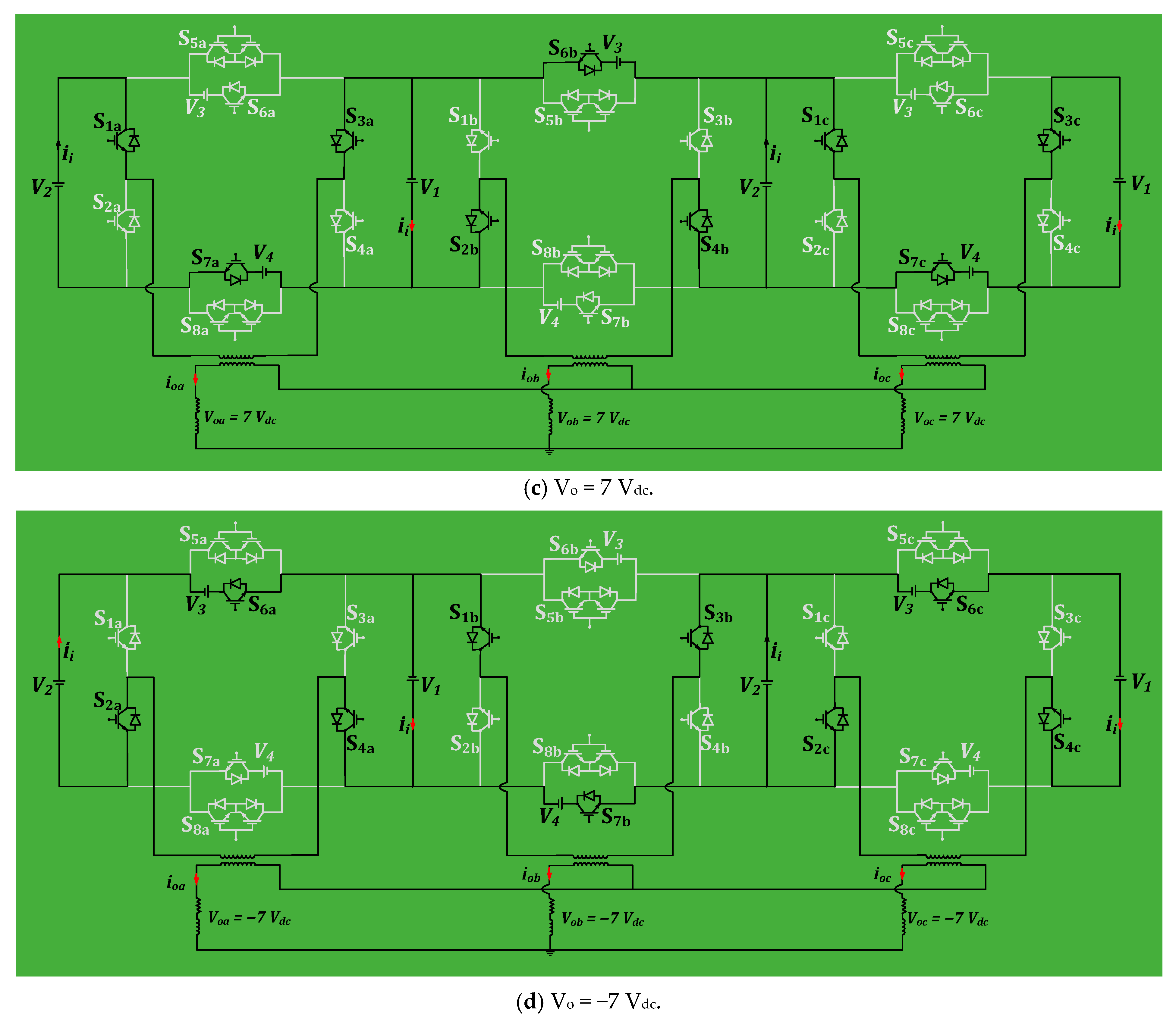
The proposed three-phase MLI is an improved architecture of the conventional H-bridge inverter. Three DC voltages and four semiconductor-based switches are incorporated into the design of the classical single-phase H-bridge inverter. Therefore, the resulting new single-phase topology has one voltage source on each of the upper, lower, left, and right sides, connected in series. Each of these sides has two switches. One of the switches on the upper and lower sides is bidirectional and derived from the common emitter configuration. Using the new methodology called the “extension technique” [21], which reduces the DC source count, the proposed three-phase MLI is illustrated in Figure 2. Considering Figure 2, the component count for the proposed three-phase MLI is ten DC sources and twenty-four power switches. The proposed three-phase MLI can be used with or without transformers. For galvanic isolation purposes, such as in DVR applications, three single-phase transformers are included in the circuit of the proposed topology. Individual phases of the proposed inverter generate 15 levels of load voltage. Two DC voltage sources per phase on the right and left sides have asymmetric characteristics. Using a DC source with symmetric characteristics will reduce the levels of load voltage. The upper and lower DC sources are equal in magnitude but not equivalent to the other two DC sources. Therefore, the proposed topology has asymmetric characteristics from a voltage point of view. This characteristic enables the generation of higher load levels juxtaposed with symmetric characteristics. If an equal voltage magnitude (symmetric) is chosen at the input of the inverter, fewer step load voltages will be produced. Comparatively asymmetric and symmetric features of the proposed inverter generate 15 and 9 voltage levels, accordingly. Connecting the DC sources in any sequence other than series will reduce the levels of load voltage produced. The switching sequences of the proposed topology are illustrated in Table 1, only showing active switches for each mode of operation. All switches in each phase contain letters A, B, and C in their subscript to show the phase they represent; thus, A, B, and C connote phase A, phase B, and phase C, accordingly. Figure 3 shows the conducting switches and current paths for some selected modes of operation.
Figure 2.
Proposed three-phase multilevel inverter.
Table 1.
Switching sequence.
Figure 3.
Conducting switches of selected switching modes.
The per-phase switching sequence of the proposed MLI is similar to that of the classical single-phase H-bridge. Positive or negative load voltages are produced by a diagonal switching sequence. The upper and lower switches are gated to provide a path for the generation of these voltages but are noted as gated ON or OFF concurrently. Considering Equations (1)–(5) and acceptable switching sequences, the maximum levels of load voltage that the proposed topology can generate are shown in Table 1. The fundamental frequency control (FFC) method is employed for the safe switching of the proposed MLI because FFC provides the following advantages against conventional PWM techniques in medium- and high-power applications: minimum switching losses, low EMI and dv/dt interference, easy to control and implement, suited for medium–high-voltage and medium–high power applications, reduced harmonic content at high levels, etc. FFC utilizes fewer switching transitions periodically compared to PWM, which operates at a high frequency, thus resulting in a higher number of switching events per cycle. A smaller number of switching events per cycle provides less thermal stress and fewer switching losses in the semiconductor switches. Therefore, these advantages make the proposed DVR reliable and efficient [6,10,12]. The junction temperatures in PWM-controlled MLI are high, culminating in higher losses; the thermal management in these devices is complex [6]. PWM techniques require pinpoint carrier integration [9] and a high-bandwidth controller, but FFC operates with minimal processing necessities [22], unsophisticated control structures, and enhanced durability to noise computation [23].
The magnitude of the source voltages is expressed by the following:
The line and phase voltages are related by the following:
Finally, the following is evident from Figure 2:
The per-phase peak voltage for the proposed topology is computed as follows:
The maximum line-to-line output voltage is expressed as follows:
3. Proposed Three-Phase MLI-Based DVR
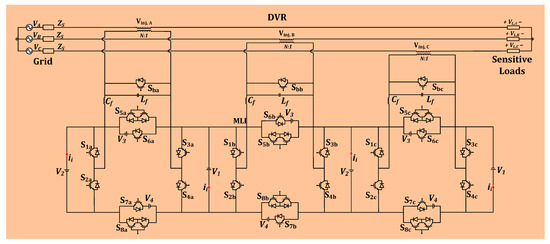
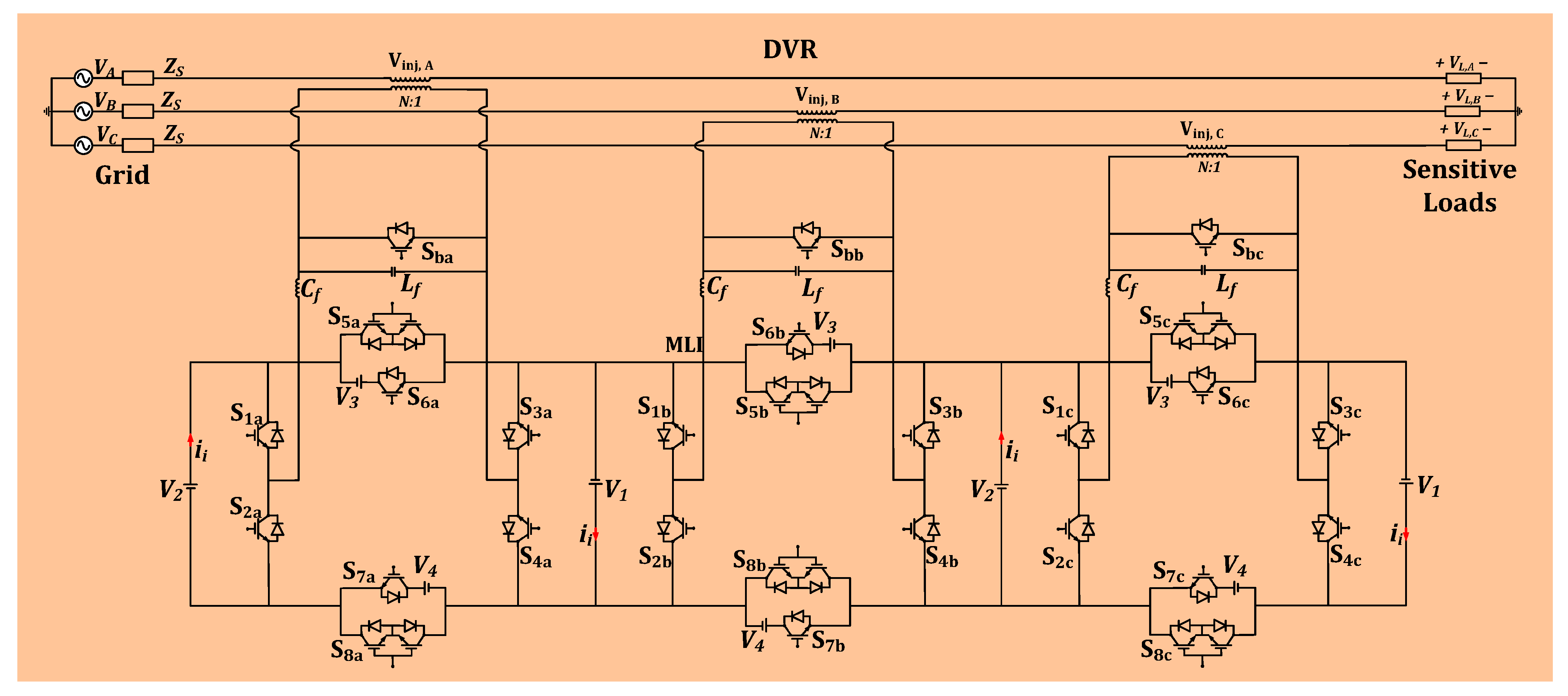
The circuit architecture of the proposed three-phase multilevel inverter-based DVR is shown in Figure 4. The proposed dynamic voltage restorer is composed of the following parts: three-phase MLI, output filter, bypass switches , , , and an injection transformer. Other parts of the system are the grid voltage and the sensitive load. As depicted by Figure 4, the proposed three-phase DVR uses an external energy source (inverter DC source voltage) to compensate for voltage sag or swell disturbances. Also, each phase of the MLI requires one low-frequency transformer, which also functions as the injection transformer and a galvanic isolator.
Figure 4.
Proposed MLI-based DVR.
3.1. Principle of Operation
The operational principle of the proposed DVR based on a three-phase MLI is categorized into two states: zero voltage-compensating or bypass state and voltage-compensating state.
- In the bypass or zero-voltage-compensating state, zero voltage is generated by each phase of the three-phase MLI and injected into the grid by turning on the bypass switches , , and . This is because the grid voltage is at its nominal value due to the absence of voltage sag or voltage swell disturbances; hence, compensating voltage is not required.
- During voltage sag or swell disturbance, the compensation state is activated. Therefore, an opposite polarity voltage of equal magnitude and phase is generated by the three-phase inverter to mitigate voltage sag or swell disturbances.
3.2. Proposed DVR Compensation
In general, DVRs fed by DC sources, such as MLI, are limited by the magnitude and period of compensating voltage. These limitations are no longer major drawbacks, due to the proliferation of photovoltaic systems for power generation. In the proposed DVR, compensating energy is derived from the inverter DC-link (battery); therefore, compensating magnitudes are hugely dependent on the magnitude of the DC-link and the maximum output voltage of the MLI. The generalized compensating magnitude of the proposed dynamic voltage restorer is presented in this section. The maximum inverter output voltage, , of the proposed DVR is expressed by Equation (6).
The general relationship between the grid voltage, DVR voltage, and load voltage of the proposed DVR of Figure 4 is determined by KVL analysis of Figure 2, which yields Equation (7). Due to the symmetry of the phases, KVL analysis of phase A yields Equation (8), which applies to the other phases.
where , , and represent grid voltage, load voltage, and DVR voltage, accordingly. Respective phase parameters have A, B, and C as initial subscripts. The inverter output voltage, , and injected DVR voltage, , of Figure 4 are related by the equation below:
Assuming is the transfer ratio of the inverter, expressed by Equation (10), then the inverter output voltage and grid voltage VG are related by Equation (11).
Equation (12) shows the needed computation during swell and sag occurrences, where and represent swell and sag voltages, respectively.
From Equation (11), represents the reference line voltage. Considering the sag phenomenon, is greater than ; therefore, has positive polarity. Likewise, during the swell phenomenon, is less than ; therefore, has negative polarity. Therefore, the proposed MLI produces the required voltage () with positive and negative polarities to offset the sag and swell phenomena, as expressed by Equation (13).
4. Simulation and Experimental Results
In this section, theoretical analysis of the proposed topology is validated by conducting simulations and experimental investigations. The experimental and simulation outcomes showcase the practicality of the proposed DVR, based on a three-phase MLI. This section is segmented into two sections; in the first section, simulation-based results of the proposed MLI topology are provided. The second section provides the experimental results of the proposed DVR, based on three-phase MLI.
4.1. Simulation Results
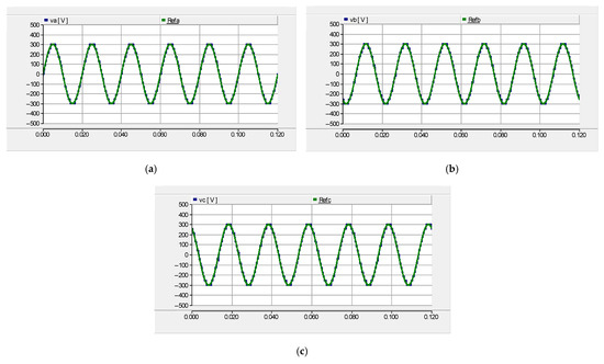
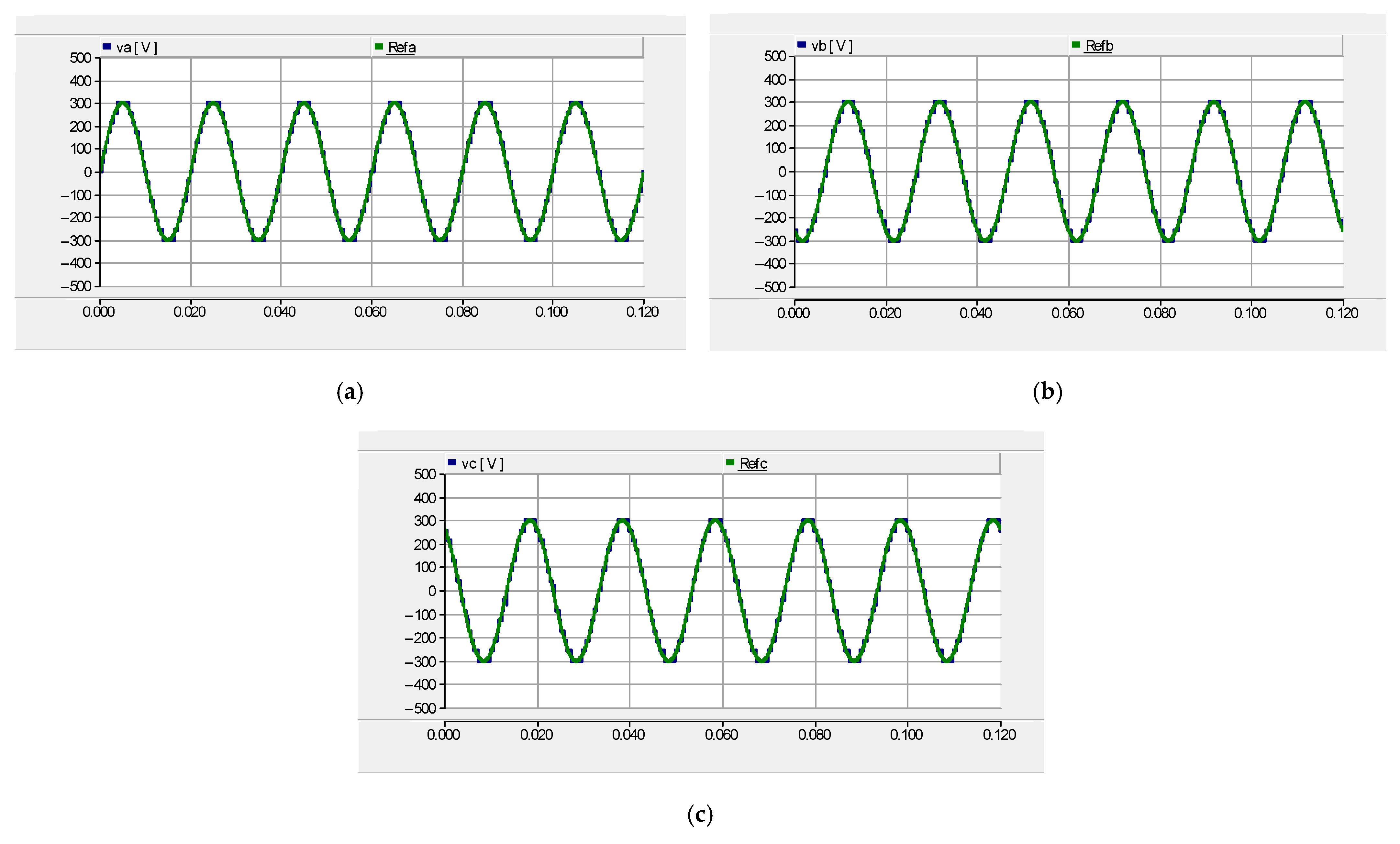
Simulation results of the proposed three-phase MLI are derived by modeling its power circuit in PSCAD/EMTDC software. The proposed three-phase MLI has an RL load connected in a Y configuration. The transformers used provide galvanic isolation with a turns ratio of . Relevant control techniques that are capable of producing quality output waveforms, reduced switching losses, and harmonics are essential for enabling the switching sequence of Table 1. Therefore, fundamental frequency modulation, also known as the nearest zero technique, is selected for switching the proposed MLI. Also, its switching losses are comparatively less when juxtaposed with the sinusoidal PWM and other PWM techniques. Using the experimental and simulation parameters of Table 2, the output waveforms of the simulation are illustrated in Figure 5, Figure 6, Figure 7, Figure 8 and Figure 9. The step (va, vb, and vc) and reference (Refa, Refb, and Refc) load voltage waveforms of all the phases, having a peak value of 300 V, are shown in Figure 5a–c accordingly. Both waveforms (step and reference) are aligned properly; therefore, the load voltage is a pure sinusoidal waveform.
Table 2.
Simulation and experimental parameters.
Figure 5.
Phase voltage waveforms. (a) phase A voltage waveform; (b) phase B voltage waveform; (c) phase C voltage waveform.
Figure 6.
Line-to-line voltage waveform.
Figure 7.
Load current waveform.
Figure 8.
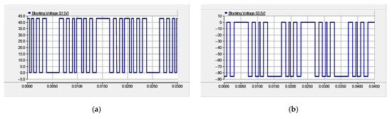
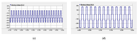
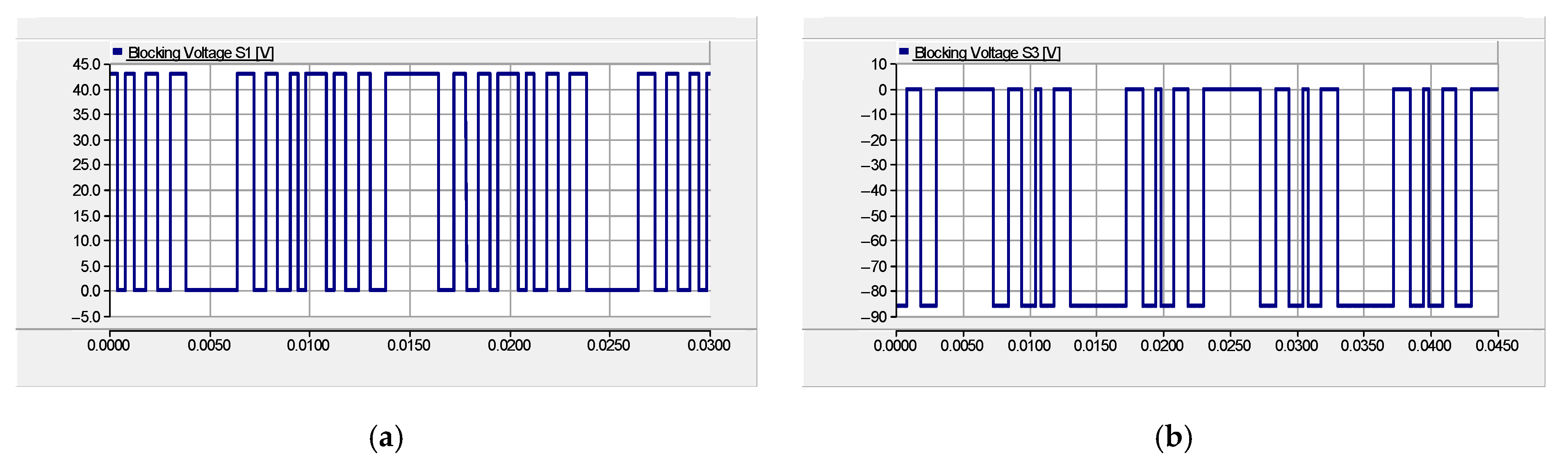
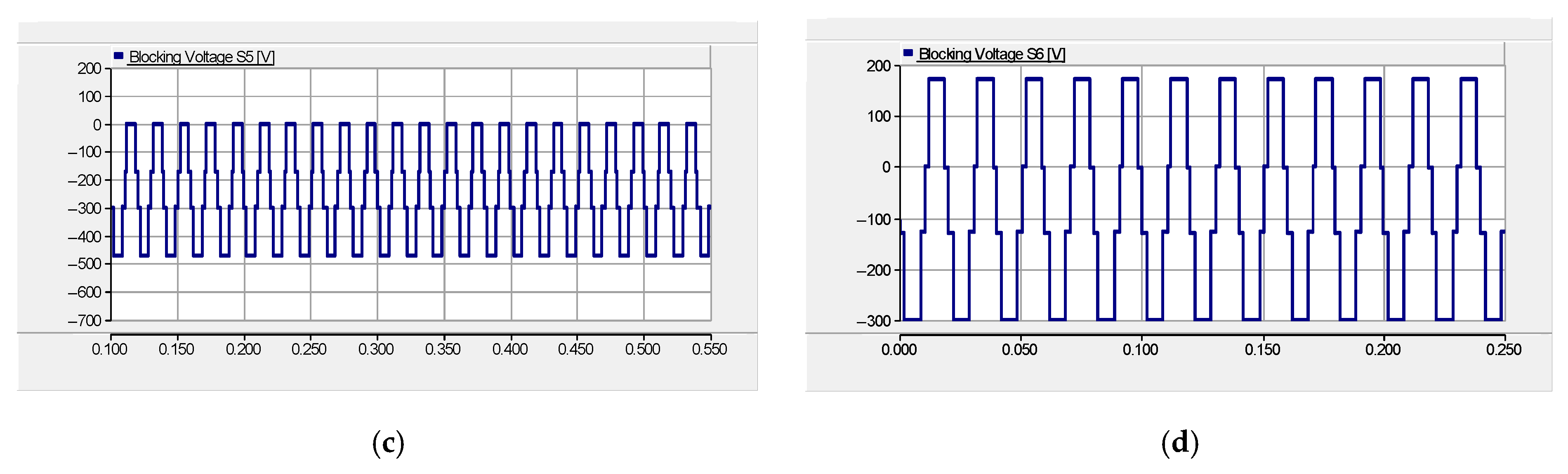
Blocking voltage waveforms. (a) switch 1; (b) switch 3; (c)switch 5; (d) switch 6.
Figure 9.
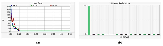
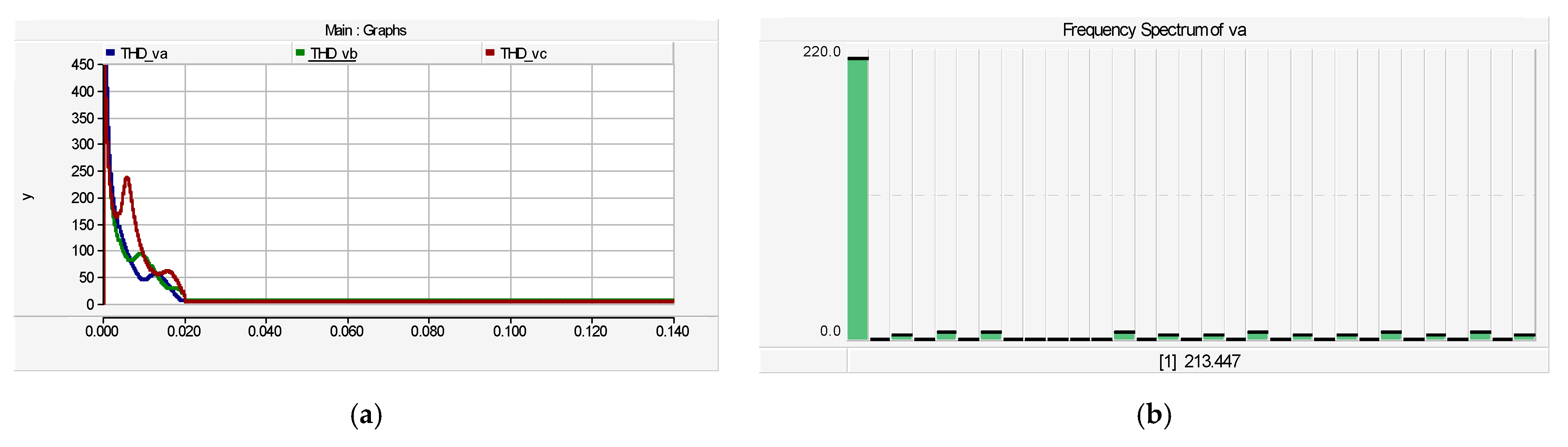
THD and FTT voltage waveforms. (a) THD waveform; (b) FFT waveform.
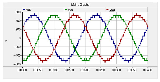
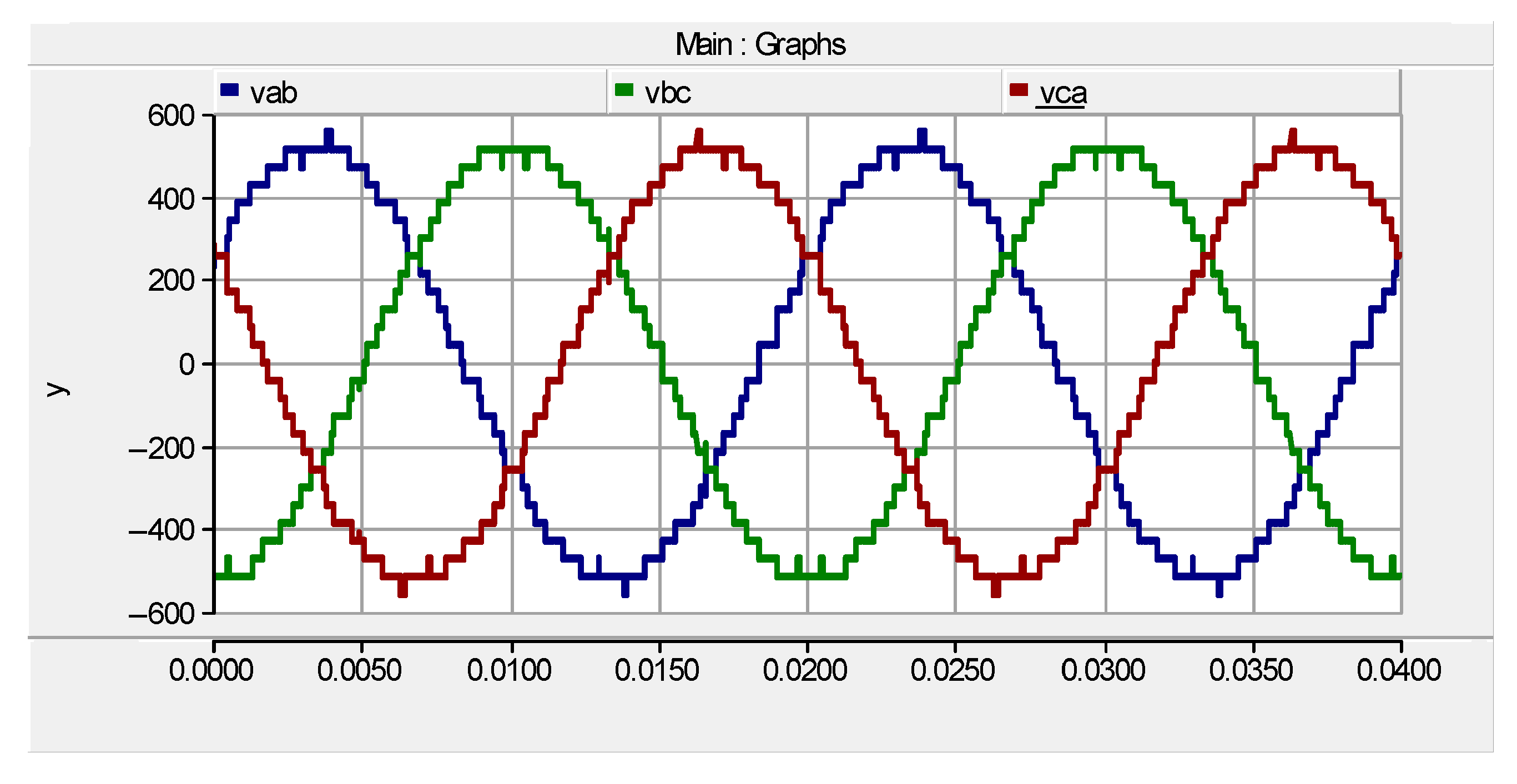
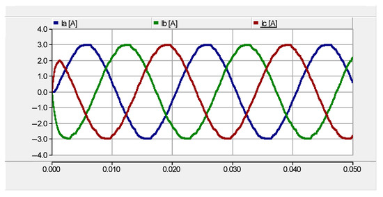
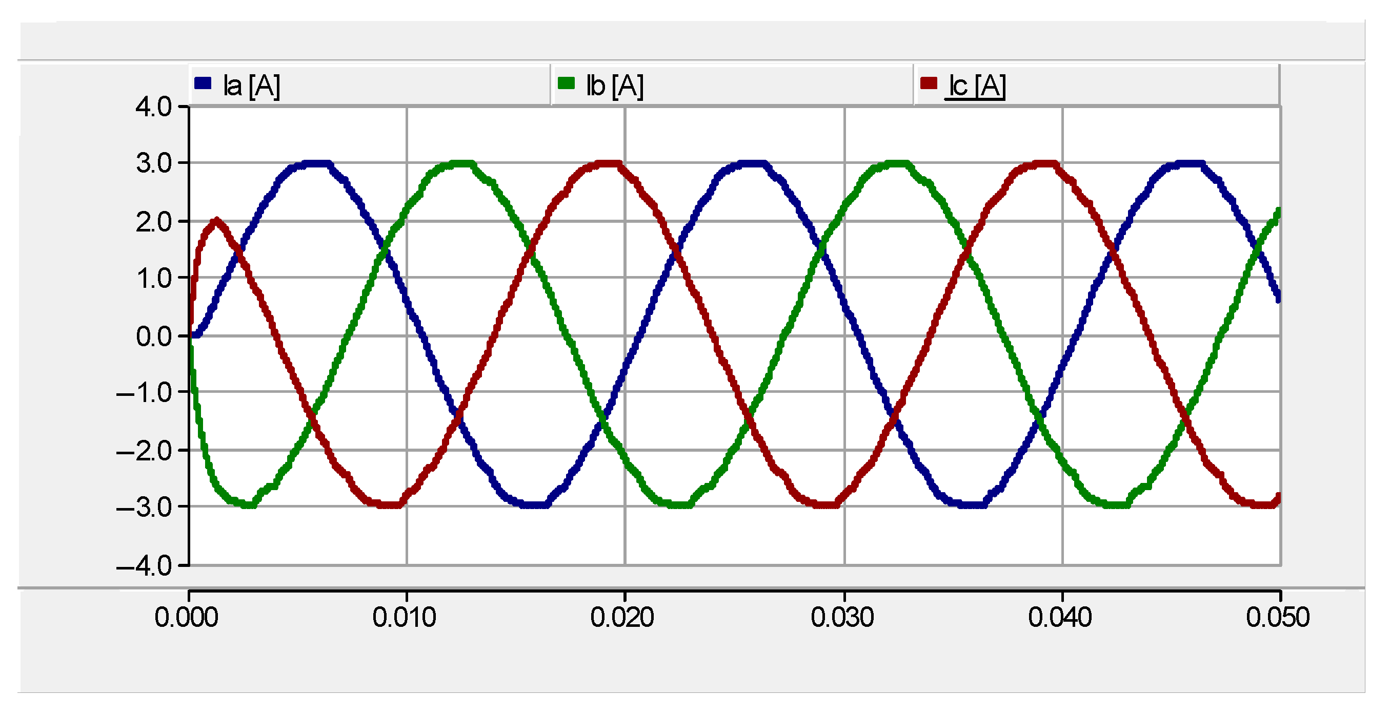
The line-line load voltage waveforms for phases AB, BC, and CA with an approximate maximum magnitude of 520 V are illustrated in Figure 6. The load current waveforms illustrated in Figure 7 exhibit pure sinusoidal waveform characteristics. Therefore, the proposed topology does not require an output filter; hence, the cost, volume, and weight of the propounded topology are not increased. The peak magnitude of the current waveforms is 3 A. Figure 8 shows the blocking voltages of some selected switches in Phase A. Switches on the same leg of connection or current path have an equal magnitude of blocking voltage, i.e., S1 and S2 are equal, S3 and S4 are equal, S5 and S7 are equal, and S6 and S8 are equal.
Figure 9a,b show the voltage THD and frequency spectrum, respectively, of the proposed three-phase multilevel inverter. From Figure 9a, the THD value of approximately 5.8% for each phase is less than the 8% IEEE 519-2022 standard [24] at the PPC (point of common coupling). The THD waveform of Figure 9a is composed of a transient period, , and the steady state period, , and were simulated using the phase load voltages of the three-phase multilevel inverter. Also, the frequency spectrum of Figure 9b shows that the harmonics’ magnitude is within acceptable ranges. The even-order harmonics are naturally zero (0), and some of the odd-order harmonics are significantly minimized. The third, fifth, and seventh harmonics are high, but within the IEEE 519-2022 acceptable range of 8% and 1.5% for low and high voltages, respectively.
4.2. Experimental Results
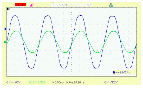
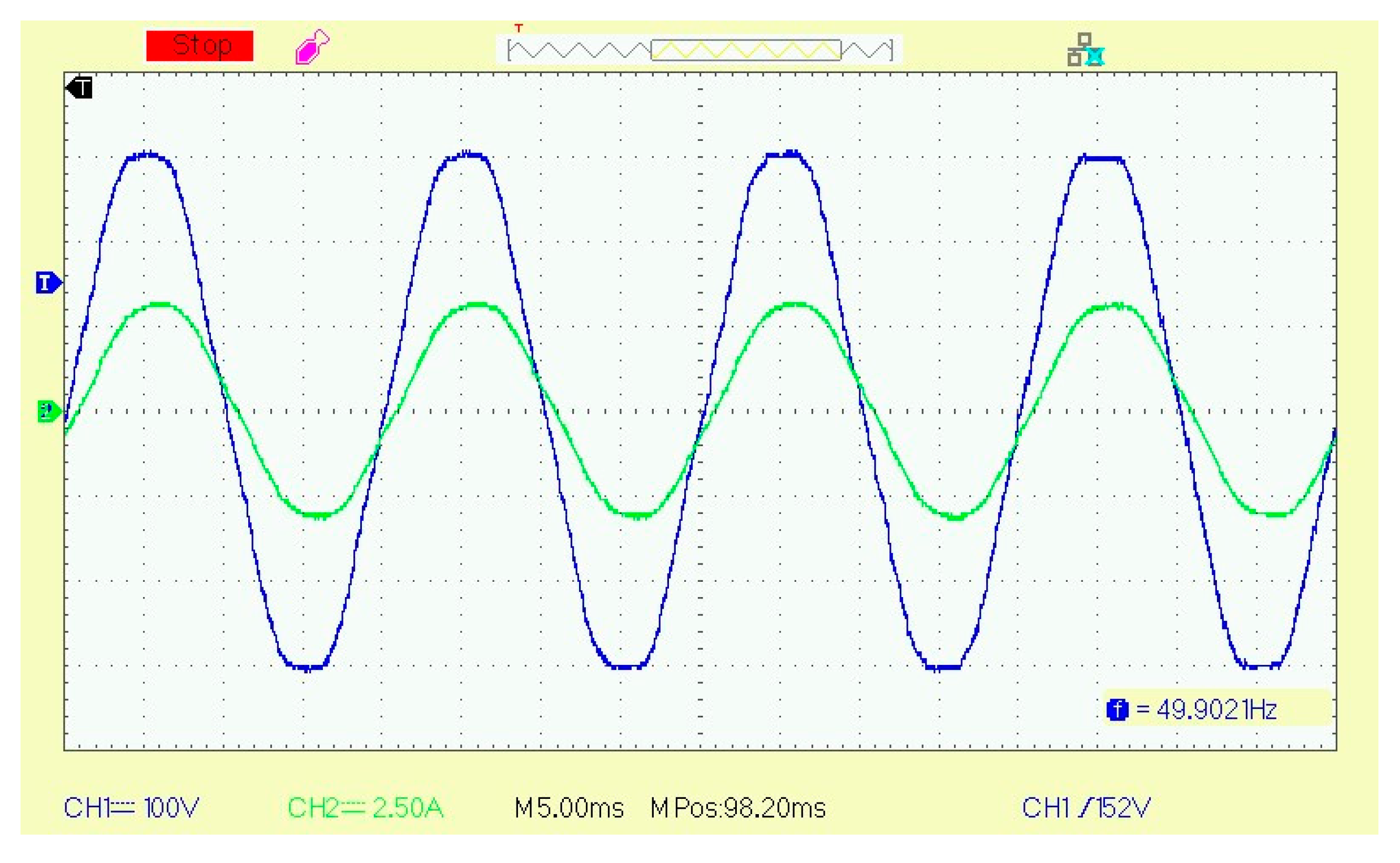
This section provides the experimental results of the proposed DVR topology, considering voltage sag and swell fault states for linear and nonlinear loads. The 20% sag and 30% sag and swell fault conditions are investigated for the linear and nonlinear loads, respectively. The laboratory setup of the proposed DVR, based on a three-phase multilevel inverter, is built using the parameters of Table 2 and source voltages expressed by Equation (14). Due to the operational similarities between the phases of the three-phase MLI, experimental analysis and results are produced for Phase A only. Nonetheless, the source voltage equations are expressed for the three phases, as in the case of Equation (14). Figure 10 illustrates the experimental waveform of the load current (green color) and voltage (blue color) for Phase A of the proposed three-phase MLI. The peak magnitude of the current and voltage waveforms is 3 A and 300 V, respectively.
Figure 10.
Phase A load voltage and current waveforms.
The proposed DVR’s operations under normal, sag, and swell fault conditions are examined in this section. The following assumptions are made for this analysis. The input three-phase voltages (, , and ) in the normal condition are as follows:
4.2.1. Normal Operating Condition
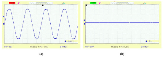
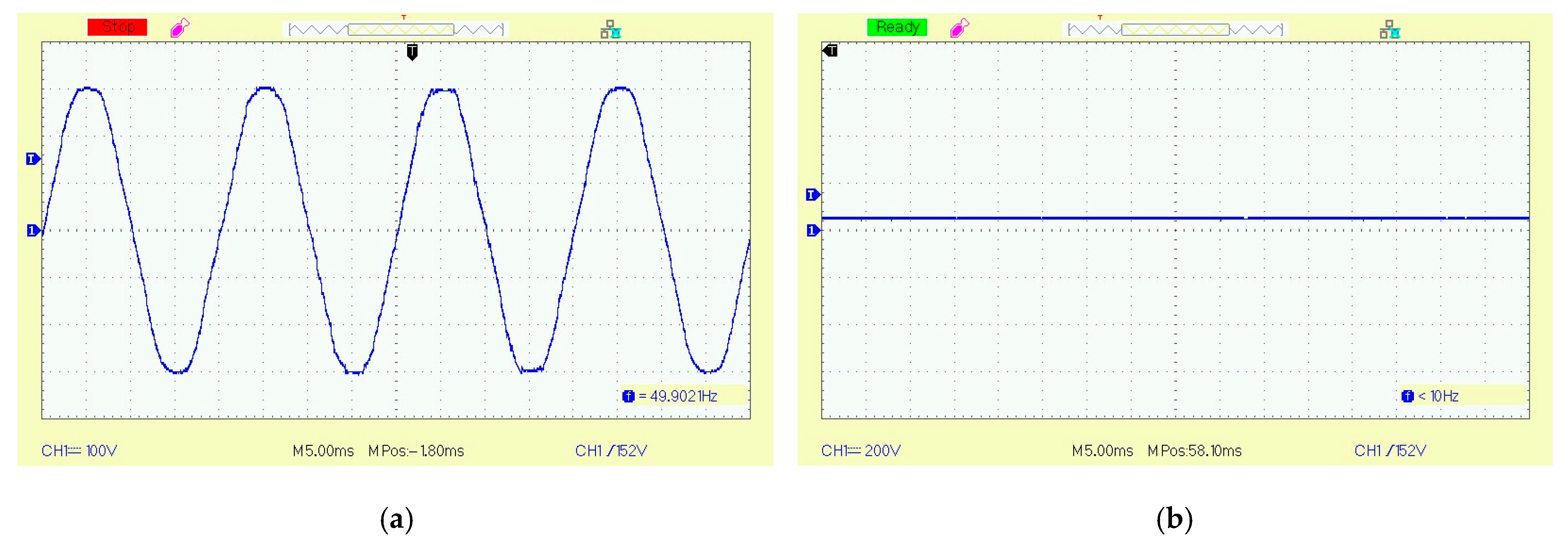
The load voltage across Phases A, B, and C is denoted by , , and , accordingly. Figure 11a shows the grid voltage for normal operation, i.e., this period is devoid of any fault condition; therefore, the injected voltage from the DVR is zero voltage (0 V), as illustrated by Figure 11b.
Figure 11.
Grid voltage and injected voltage during normal operating mode. (a) grid voltage; (b) injected voltage.
4.2.2. Linear Loads
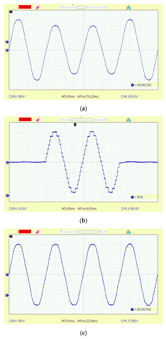
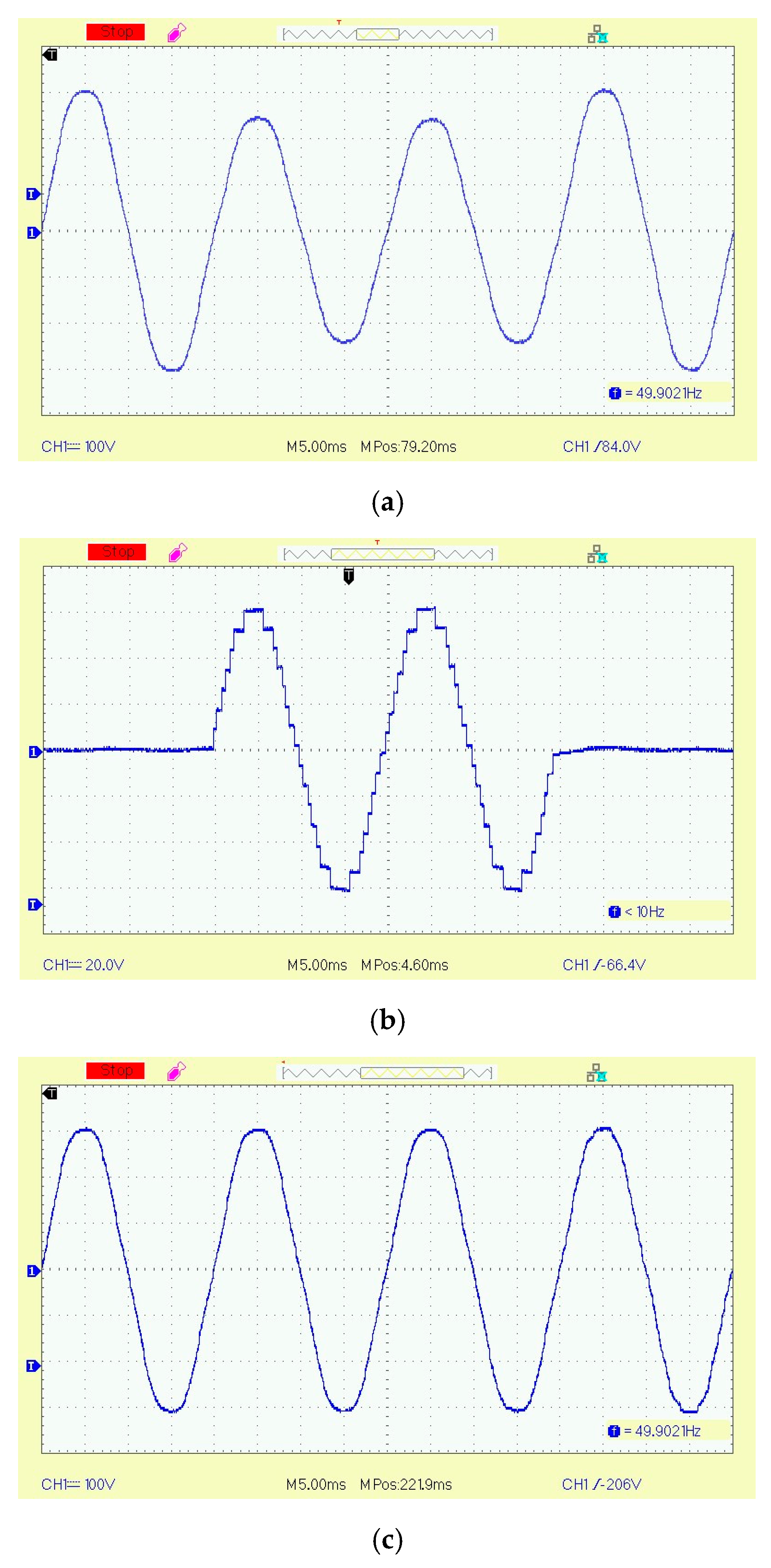
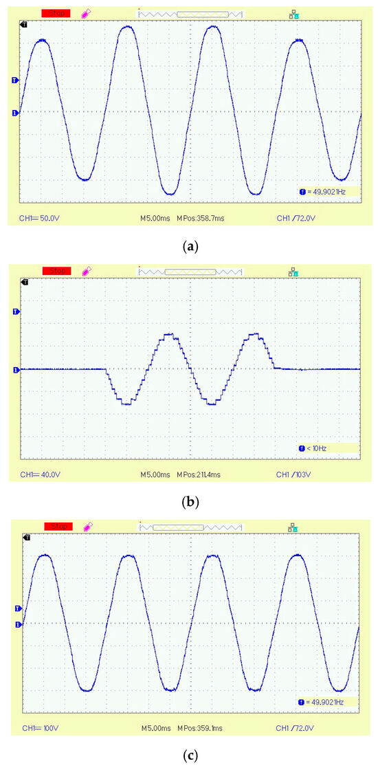
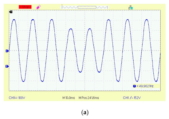
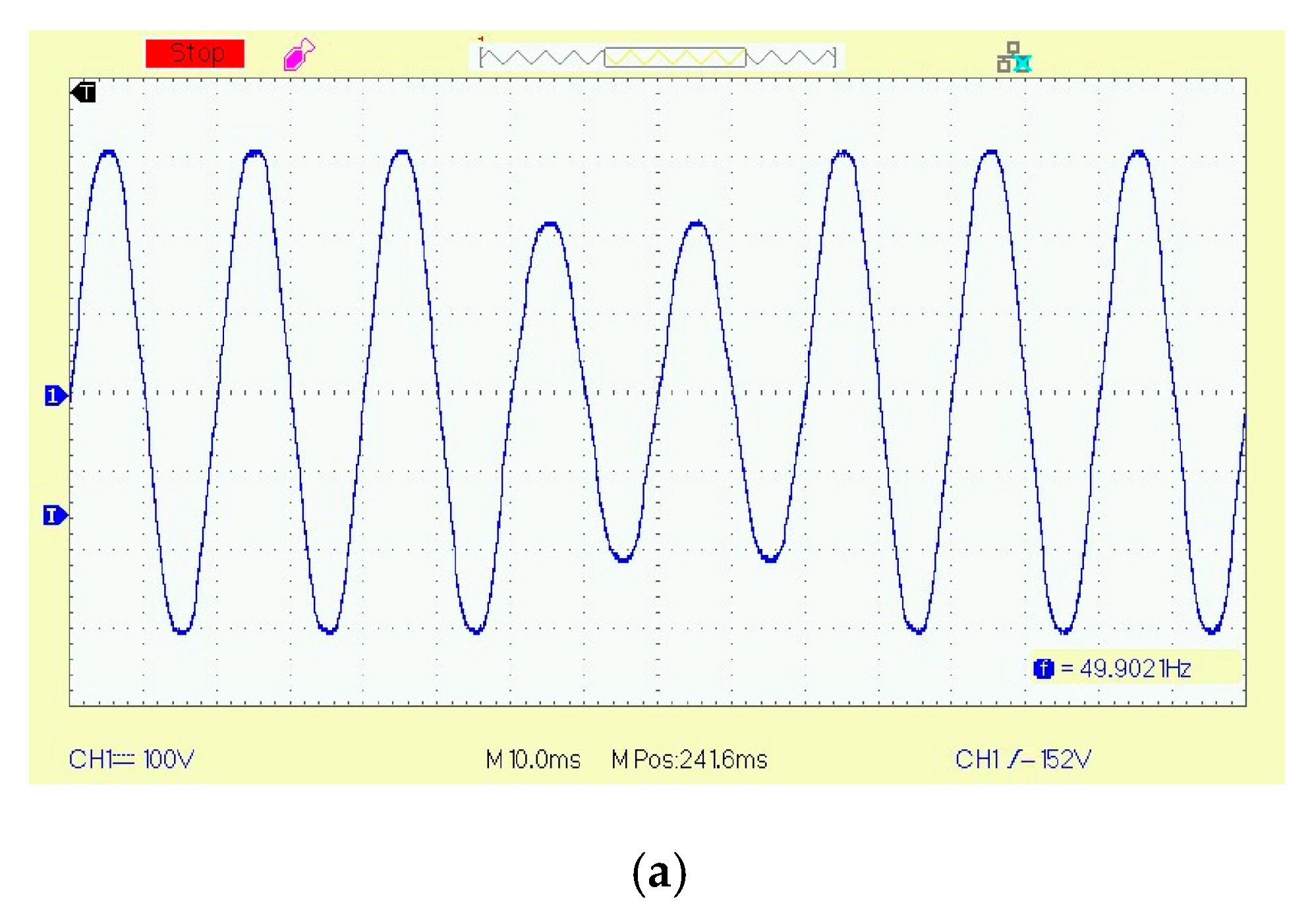
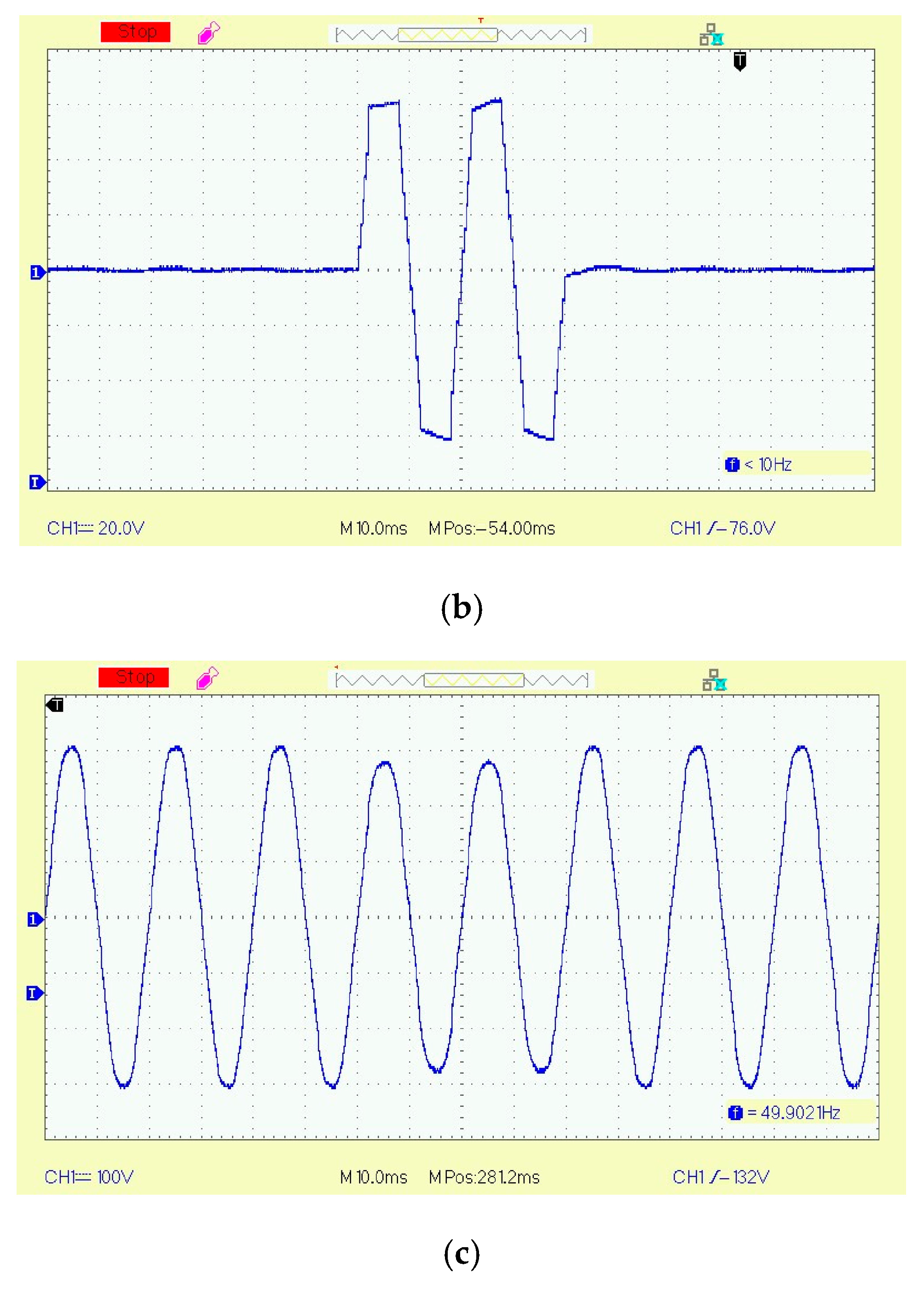
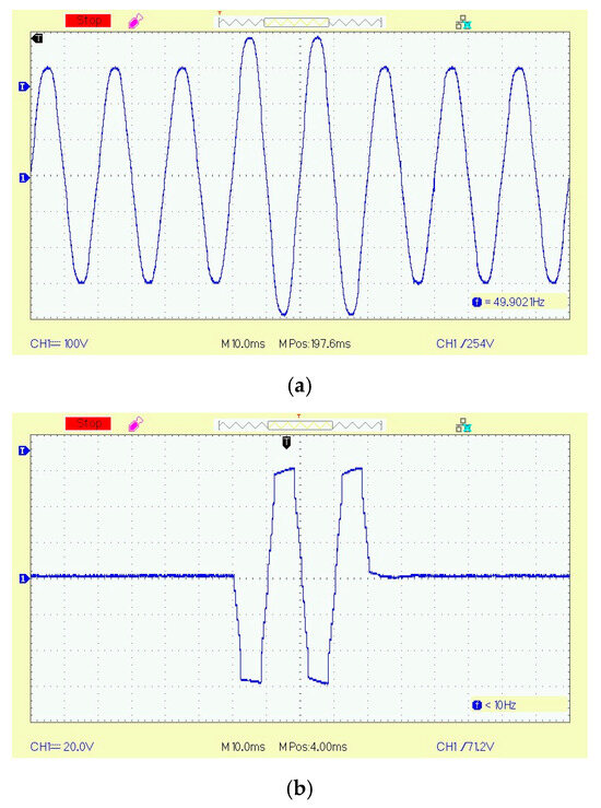
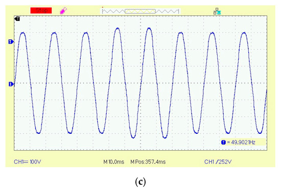
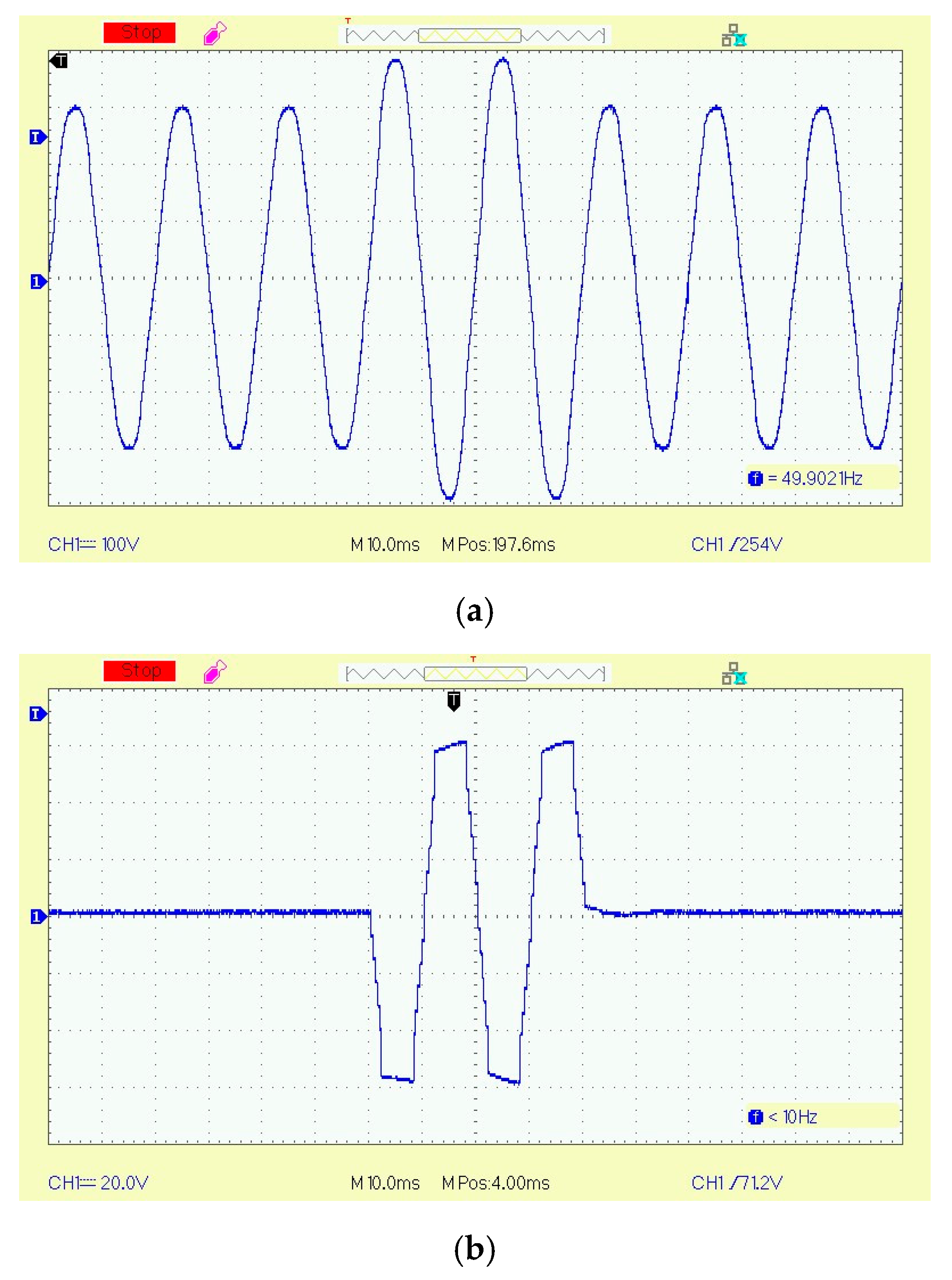
Considering the sag–swell fault conditions under investigation for linear loads, it is expected that under sag conditions, the proposed MLI injects a positive difference voltage to keep the three-phase load voltage constant. However, during swell conditions, the multilevel inverter injects a negative difference voltage with a 180° phase difference to offset the disturbance and restore the load voltage to the nominal value. In this experiment, the grid’s voltage is expressed by Equation (14) for rated conditions. During the sag and swell period, the rated voltage reduces and increases by 0.8% and 1.2%, respectively. The sag mode is expressed by Equation (15) for the time interval of and the swell mode is expressed by Equation (16) for the time interval of . Also, the faultless period of operation of the proposed DVR occurs during the time intervals of and . These faultless and faulty states of operations of the proposed DVR are illustrated in Figure 12 and Figure 13 for the sag and swell states, respectively.
Figure 12.
Sag state for linear loads. (a) sag voltage waveform; (b) injected voltage waveform; (c) restored nominal voltage waveform.
Figure 13.
Swell state for linear loads. (a) swell voltage waveform; (b) injected voltage waveform; (c) restored nominal voltage waveform.
To resolve the above sag–swell issues, the DVR needs to inject the required voltages to offset or compensate for these anomalies. Figure 12a and Figure 13a show the line voltages under faulty conditions. Figure 12b and Figure 13b show the required injected voltage to compensate for the sag–swell faults, respectively. During the time interval of , the DVR injects the required magnitude of voltage in phase with the line voltage to mitigate the decrease in the rated voltage. Similarly, during the time interval of , the DVR injects the required voltage magnitude out of phase with the line voltage to mitigate the increase in the rated voltage. Between and , the DVR injects no voltage, because the sag–swell fault conditions are not present. Figure 13c shows the restored line voltage with a rated peak voltage of 300 V.
4.2.3. Nonlinear Loads
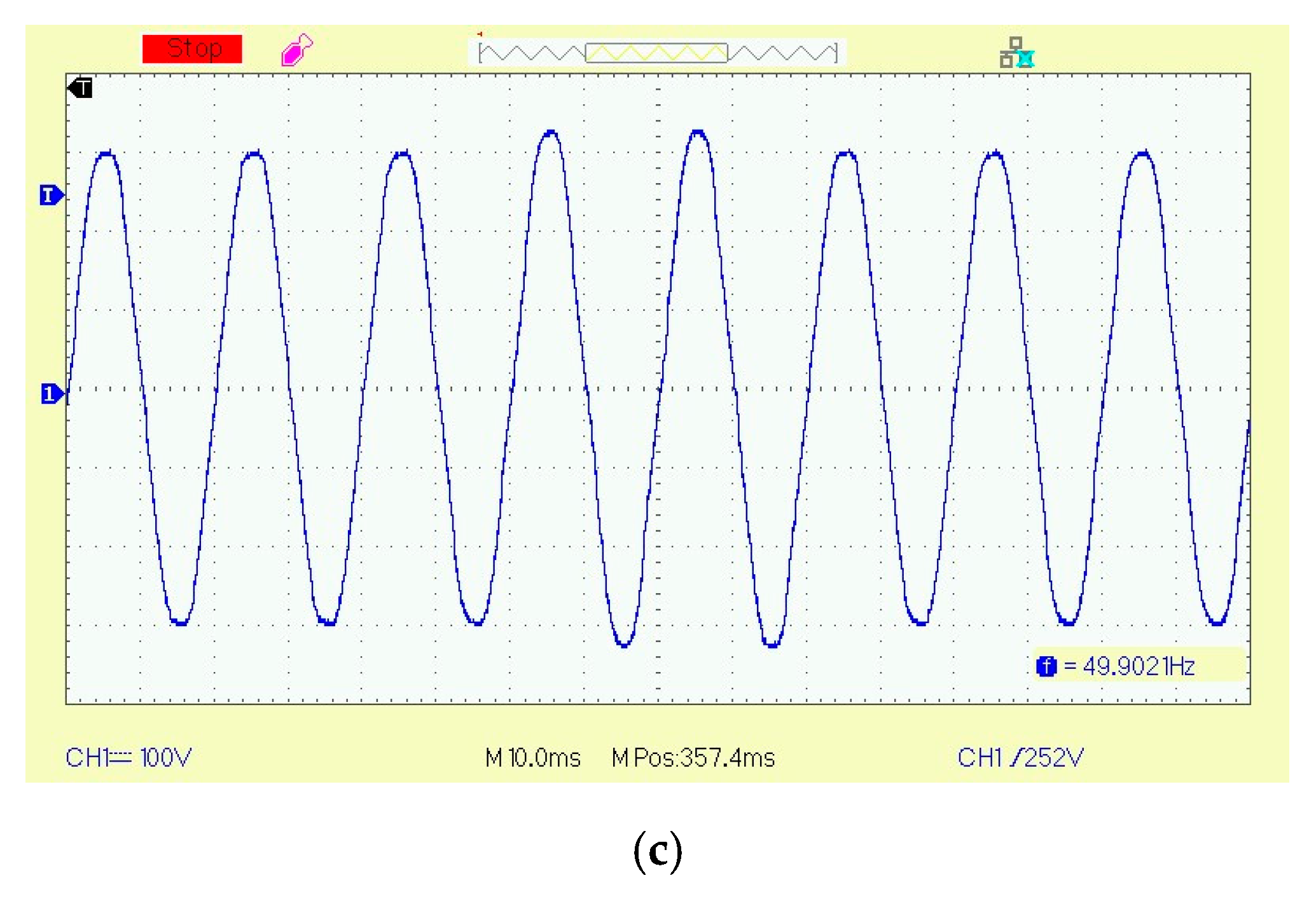
Similarly, the proposed DVR-based MLI is investigated for voltage sag and swell conditions for nonlinear loads. During the sag and swell period, the rated voltage reduces and increases by 0.7% and 1.3%, respectively, for nonlinear loads. Thus, the DVR is required to inject a voltage of 70 V in and out of phase to mitigate the sag and swell fault conditions. However, considering the maximum source voltage of the MLI, the DVR can only compensate for 86% of the sag/swell condition. Considering the sag and swell modes depicted in Figure 14a and Figure 15a, the injected voltages for compensation are shown in Figure 14b and Figure 15b, accordingly. The restored (87%) load voltage for nonlinear loads considering the sag and swell conditions is shown in Figure 14c and Figure 15c, accordingly. Only 86–87% of the load voltage is restored in this case, because of the magnitude of the incremental voltage value and the level count of the MLI. The maximum MLI output voltage and the load voltage are equal. Increasing the level count to more than 31 directly reduces the value, thus allowing for compensations at lower magnitudes.
Figure 14.
Sag state for nonlinear loads. (a) sag voltage waveform; (b) injected voltage waveform; (c) restored nominal voltage waveform.
Figure 15.
Swell state for nonlinear load. (a) swell voltage waveform; (b) injected voltage waveform; (c) restored nominal voltage waveform.
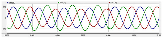
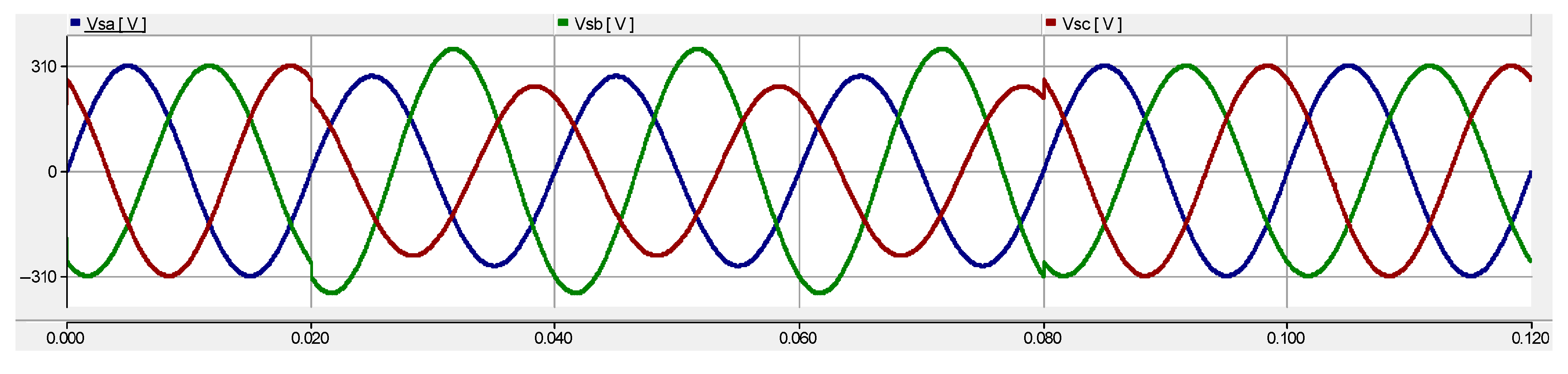
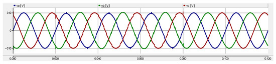
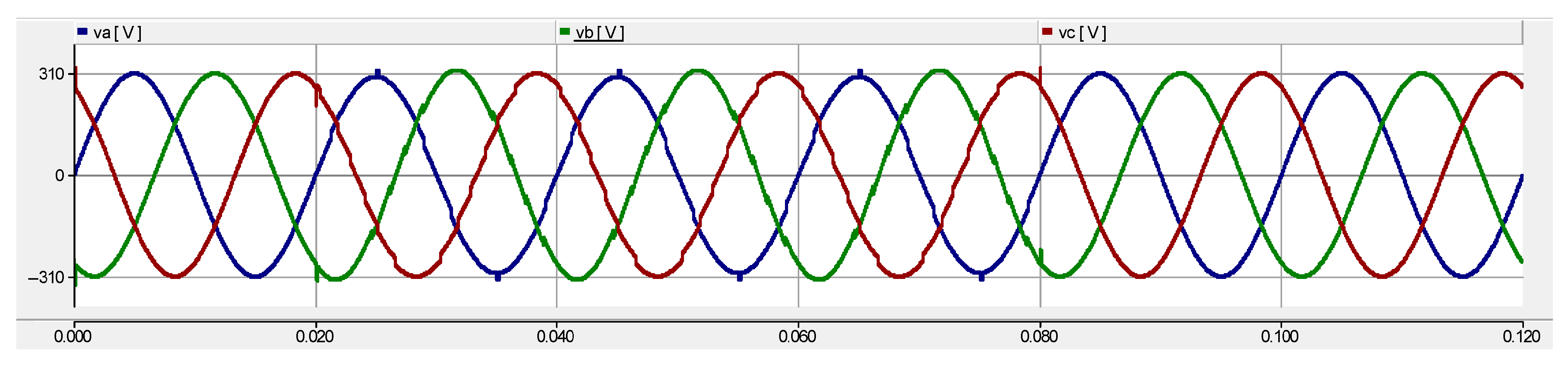
The proposed DVR is also investigated for unbalanced three-phase distortions, considering a load voltage of 310 V. Equations (18)–(20) show the load voltage waveforms during the normal operating period , faulty period , and restored (after compensation) period , respectively. Two sag cases are presented for phases A and C, with sag voltage magnitudes of 280 V and 250 V, respectively. The swell condition is analyzed in phase B, with a swell voltage magnitude of 50 V. Figure 16 and Figure 17 show the simulation results for the faulty conditions (Figure 16) and restored or compensated load voltage (Figure 17). The presence of negative-sequence components (NSC) in three-phase unbalanced loads introduces new challenges, such as complex control (NSC comes in the form of fluctuating AC quantities with double frequency, making it hard for the DVR control technique to track, maintain, and compensate them adequately), reduced performance due to the error in the compensating voltage, and DVR output voltage. Nonetheless, the application of the right control techniques, such as negative-sequence elimination (NSE), multiple DQ transformation, etc., eliminates these limitations.
Figure 16.
Three-phase unbalanced load voltage waveforms.
Figure 17.
Restored three-phase load voltage waveforms.
4.2.4. Compensation Limitations
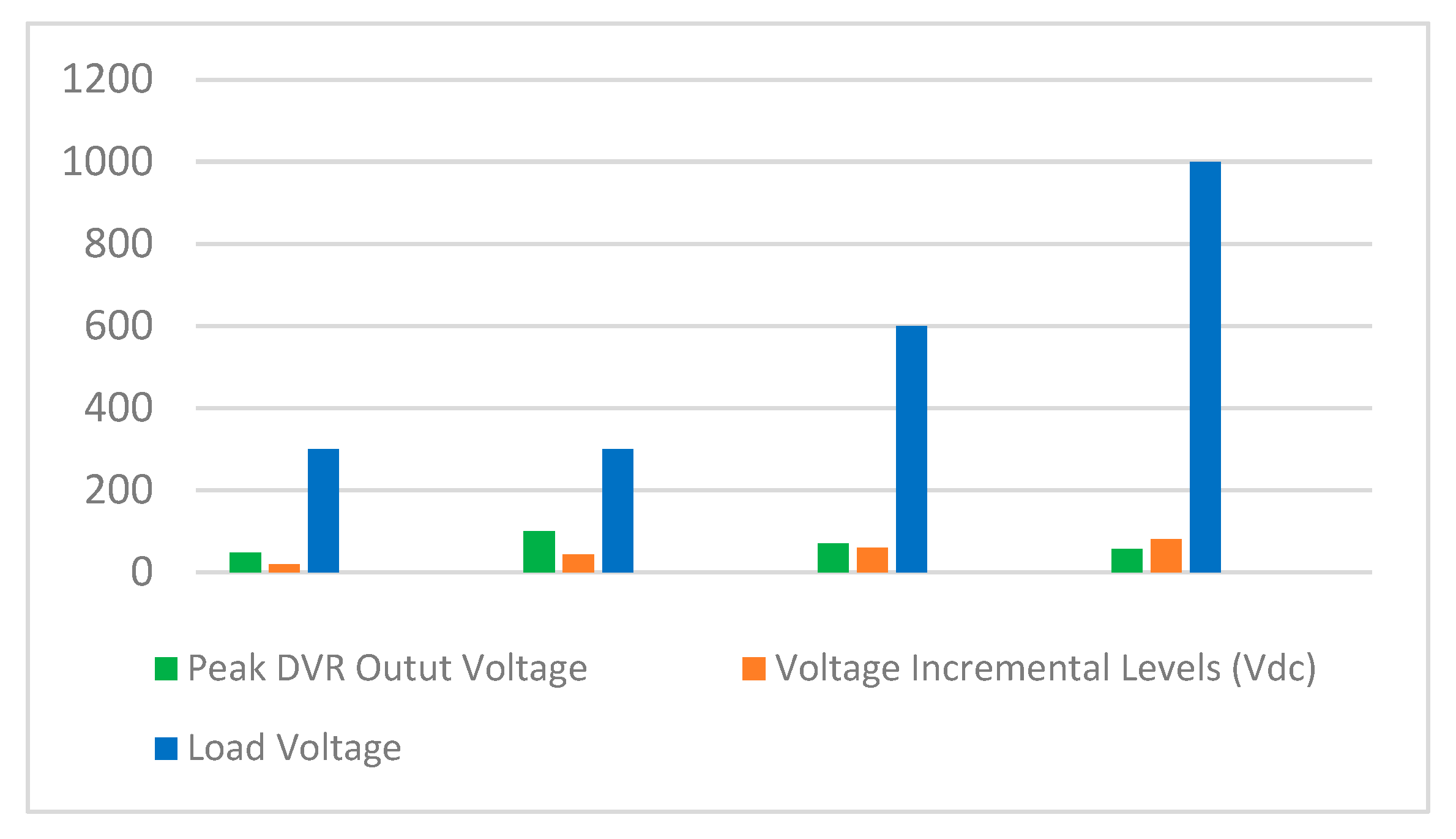
The primary function of a DVR is to mitigate power quality issues, such as voltage swell and dip, by injecting voltage of an appropriate magnitude and phase. Therefore, the magnitude of the compensating voltage should be suitable to offset any power disturbance. This section investigates the proposed DVR’s compensating capabilities, considering critical DVR parameters such as peak voltages of the DVR, incremental voltage values, compensating percentages, etc., for the varying input voltages provided in Table 3. The major limitations of most DVRs are the magnitude of the compensating voltage and the compensating duration capabilities. From Table 3, it is evident that the proposed DVR can compensate for any voltage sag or swell conditions if the MLI input voltage is varied.
Table 3.
Limitation analysis of the proposed three-phase MLI-based DVR.
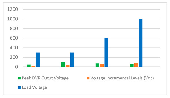
However, because the incremental voltage levels are dependent on the magnitude of Vdc, and the DVR voltage output levels are 15, this may impose some limitations on the compensating duration and voltage magnitude. The maximum compensating voltage and compensating percentage that the proposed DVR can deliver at any time are based on the magnitude of the source voltages V1, V2, and V3/V4. For example, if V1 = 20 V, V2 = 40 V, and V3 = V4 = 80 V, and the load voltage is 300 V, the proposed DVR can provide 46.67% of compensation (sag or swell), with an incremental voltage level of 20V. Similarly, if V1 = 42.85 V, V2 = 85.70 V, and V3 = V4 = 171.40 V, and the load voltage is 300 V, the proposed DVR can provide 46.67% of compensation (sag or swell), with an incremental voltage level of 20V. The compensating duration of the proposed DVR will not be a major limitation when renewable energy sources and/or energy storage systems, such as PV, etc., are applied as the source voltage [25]. Improvements made in large-scale battery production for utility or commercial applications, such as Megapack by Tesla, can interface with PV systems and the DVR to provide compensation for long-duration disturbances. Additionally, a rectifier circuit can be used to provide power directly from the grid, as in the case of AC-DC-AC DVR topologies. The latter methodology introduces double-stage power conversion, which reduces the overall system efficiency due to multiple operations of power switching during the conduction and switching states. In the absence of the above features, the proposed DVR functions better in small-to-medium depth and duration compensation, juxtaposed with deep and prolonged compensation because of the limitation of the battery (DC-link), i.e., voltage capacity and battery life. As shown by the second (case 1) and fifth (case 4) columns of Table 3, where the load voltages far exceed the maximum MLI-DVR output voltage, the compensation capabilities of the proposed DVR are reduced during deep disturbances. Finally, the compensating capabilities of multilevel inverter-based DVRs depend on the peak magnitude of the DVR output voltage, the number of output voltage levels, the voltage’s incremental magnitude, and the lifespan of the source voltage. Figure 18 shows a graph of the major compensating parameters.
Figure 18.
Magnitude of compensating parameters.
4.2.5. Comparative Analysis
Comparative analysis of the proposed three-phase MLI DVR and existing DVRs, considering features such as phase count, control technique, stages of voltage conversion, etc., is presented in this section. The result of this comparative investigation is illustrated in Table 4. It is evident that the proposed three-phase multilevel inverter-based DVR stacks properly against existing DVR topologies. For example, the proposed DVR can adequately compensate for voltage sag and swell, as well as harmonics, in linear and nonlinear three-phase loads and unbalanced loads. Also, the compensating voltage has a single voltage conditioning feature, and the presence of a battery makes it suitable for renewable energy integration.
Table 4.
Comparative investigation [13,14,16,22,23,26,27].
The absence of a direct voltage-boosting feature in the MLI is a drawback, considering the current trajectory of multilevel inverter topologies. Having voltage-boosting capabilities, as in the case of impedance-based topologies (a common example is the Z-source), will provide a longer cycle life for the source voltage (battery) and will also enable the DVR to compensate for deep sag/swell conditions and for longer duration without putting much stress on the battery. Nonetheless, voltage-boosting capabilities can be provided by the low-frequency transformer, which serves as the injection and galvanic isolation device. The inherent features of the low-frequency transformer directly affect the scalability and transient behavior of the proposed MLI-DVR. The winding resistance and leakage inductance are increased because of the bulkiness of the transformer, due to its operations at the fundamental network frequency. Increased winding resistance and leakage inductance cause losses, reduced efficiency, and reduced voltage injection response time during an abrupt grid disruption. Also, thermal limitations and transient magnetic saturation can establish nonlinear characteristics, causing a reduction in the efficacy of the compensations. In the absence of voltage-boosting features, the proposed MLI-DVR is highly suited for applications in grid networks such as distribution systems facing low-to-medium voltage sag/swell challenges (10–30%). Voltage compensation in such networks can be achieved without LDES (long-duration energy storage) or boost DC-DC converters. The inherent advantages of MLIs (better voltage synthesizing and superior quality waveforms) produce voltage waveforms with low THD, thus complying with industry standards such as IEEE 519. These features make the proposed topology appropriate for applications in low–medium power networks, where the protection of sensitive loads in commercial buildings, industries, and microgrid is desired. Table 5 shows a summarized presentation of the sag and swell for linear and nonlinear and unbalanced loads, considering the dip/swell percentage, the injected voltage, and the fault duration.
Table 5.
Summarized experimental DVR compensations.
5. Conclusions
A dynamic voltage restorer (DVR) is undoubtedly the most efficient power quality enhancer, considering sensitive loads and proximity to the load. This article proposes a dynamic voltage restorer based on a new three-phase MLI that is suitable for mitigating power quality challenges such as voltage dip, swell, and harmonics in power systems. The capabilities of the proposed MLI-DVR are demonstrated by simulation, using PSCAD/EMTDC software and experimental investigations. The proposed three-phase MLI generates 15 steps of load voltage using fewer components. Symmetric and asymmetric analysis of the proposed MLI source voltages confirms the generation of higher levels of load voltage from the asymmetric topology without increasing the component count or structure. The quality of the inverters’ simulated load waveforms juxtaposed with the reference waveforms is high. Similarly, experimental analysis of the proposed three-phase MLI validates the qualities of the simulated waveforms by using the fundamental frequency control technique. Simulated THD and FFT values are within acceptable standards, like IEEE 519-2022. The proposed MLI-DVR is investigated during normal operations and fault conditions, such as voltage dip and voltage swell for linear and nonlinear loads, and unbalanced loads, where the proposed DVR adequately mitigated the power disturbances and restored the voltage magnitude to the nominal value; thus, attesting to the practicality of the proposed DVR topology. Also, a comparative analysis of the proposed DVR and existing DVR topologies is conducted.
Author Contributions
Conceptualization, S.N.T.; methodology, E.B., Ş.B., and Ö.C.Ö.; software, S.N.T. and E.B.; validation, Ö.C.Ö., M.F., and Ş.B.; formal analysis, Ş.B., Ö.C.Ö., and M.F.; investigation E.B., Ö.C.Ö., and Ş.B.; writing—original draft preparation, S.N.T., E.B., Ş.B., Ö.C.Ö., and M.F.; writing—review and editing, M.F., Ş.B., E.B., and Ö.C.Ö.; visualization M.F., S.N.T., and E.B.; supervision, E.B., Ş.B., Ö.C.Ö., and M.F. All authors have read and agreed to the published version of the manuscript.
Funding
This research received no external funding.
Data Availability Statement
The original contributions presented in this study are included in the article. Further inquiries can be directed to the corresponding author.
Conflicts of Interest
The authors declare no conflicts of interest.
References
- Elnady, A.; Salama, M.M.A. Mitigation of Voltage Disturbances Using Adaptive Perceptron-Based Control Algorithm. IEEE Trans. Power Deliv. 2005, 20, 309–318. [Google Scholar] [CrossRef] [Scilit]
- Jimichi, T.; Fujita, H.; Akagi, H. Design and Experimentation of a Dynamic Voltage Restorer Capable of Significantly Reducing an Energy-Storage Element. IEEE Trans. Ind. Appl. 2008, 44, 817–825. [Google Scholar] [CrossRef] [Scilit]
- Chan, J.Y.; Milanovic, J.V. Assessment of the Economic Value of Voltage Sag Mitigation Devices to Sensitive Industrial Plants. IEEE Trans. Power Deliv. 2015, 30, 2374–2382. [Google Scholar] [CrossRef] [Scilit]
- IEEE Std. 1346; IEEE Recommended Practice for Evaluating Electric Power System Compatibility with Electronic Process Equipment. IEEE: Piscataway, NJ, USA, 1998.
- IEEE Std. 1159; IEEE Recommended Practice for Monitoring Electric Power Quality. IEEE: Piscataway, NJ, USA, 1995.
- Farhadi-Kangarlu, M.; Babaei, E.; Blaabjerg, F. A Comprehensive Review of Dynamic Voltage Restorers. Int. J. Electr. Power Energy Syst. 2017, 92, 136–155. [Google Scholar] [CrossRef] [Scilit]
- Bollen, M.H.J. Understanding Power Quality Problems: Voltage Sags and Interruptions; Wiley-IEEE Press: Hoboken, NJ, USA; Piscataway, NJ, USA, 2000. [Google Scholar]
- Arrillaga, J.; Watson, N.R.; Chen, S. Power System Quality Assessment; John Wiley & Sons: Chichester, UK; New York, NY, USA, 2000. [Google Scholar]
- Najafi, E.; Yatim, A.H.M. A Novel Current Mode Controller for a Static Compensator Utilizing Goertzel Algorithm to Mitigate Voltage Sags. Energy Convers. Manag. 2011, 52, 1999–2008. [Google Scholar] [CrossRef] [Scilit]
- Ghosh, A.; Ledwich, G. Compensation of Distribution System Voltage Using DVR. IEEE Trans. Power Deliv. 2002, 17, 1030–1036. [Google Scholar] [CrossRef] [Scilit]
- Woodley, N.H.; Morgan, L.; Sundaram, A. Experience with an Inverter-Based Dynamic Voltage Restorer. IEEE Trans. Power Deliv. 1999, 14, 1181–1186. [Google Scholar] [CrossRef] [Scilit]
- Nielsen, J.G.; Blaabjerg, F. A Detailed Comparison of System Topologies for Dynamic Voltage Restorers. IEEE Trans. Ind. Appl. 2005, 41, 1272–1280. [Google Scholar] [CrossRef] [Scilit]
- Hasan, K.; Othman, M.M.; Meraj, S.T.; Rahman, M.S.; Lipu, M.S.H.; Kotsampopoulos, P. DC-AC Converter with Dynamic Voltage Restoring Ability Based on Self-Regulated Phase Estimator-DQ Algorithm: Practical Modeling and Performance Evaluation. Electronics 2023, 12, 523. [Google Scholar] [CrossRef] [Scilit]
- Liu, D.; Zhang, H.; Liang, X.; Deng, S. Model Predictive Control for Three-Phase, Four-Leg Dynamic Voltage Restorer. Energies 2024, 17, 5622. [Google Scholar] [CrossRef] [Scilit]
- Trabelsi, M.; Komurcugil, H.; Bayhan, S.; Abu-Rub, H. An Effective Transformerless PUC7-Based Dynamic Voltage Restorer Using Model Predictive Control. Sustainability 2023, 15, 3041. [Google Scholar] [CrossRef] [Scilit]
- Khergade, A.V.; Satputaley, R.J.; Borghate, V.B.; Raghava, B.V.S. Harmonics Reduction of Adjustable Speed Drive Using Transistor Clamped H-Bridge Inverter Based DVR with Enhanced Capacitor Voltage Balancing. Trans. Ind. Appl. 2020, 56, 6744–6755. [Google Scholar] [CrossRef] [Scilit]
- Jiang, F.; Cheng, S.; Tu, C.; Guo, Q.; Li, Q.Q.; Chen, C. Optimum Control Scheme of Output Voltage Based on Cascaded H-Bridge DVR. CSEE J. Power Energy Syst. 2020, 6, 249–258. [Google Scholar] [CrossRef] [Scilit]
- Shahabadini, M.; Iman-Eini, H. Improving the Performance of a Cascaded H-Bridge-Based Interline Dynamic Voltage Restorer. IEEE Trans. Power Deliv. 2016, 31, 1160–1167. [Google Scholar] [CrossRef] [Scilit]
- Vijayalakshmi, A. Improved Trans-Z-Source Inverter Based Dynamic Voltage Restorer. Aust. J. Electr. Electron. Eng. 2021, 19, 22–30. [Google Scholar] [CrossRef] [Scilit]
- Ye, J.; Gooi, H.B.; Zhang, X.; Wang, B.; Pou, J. Simplified Four-Level Inverter-Based Dynamic Voltage Restorer with Single DC Power Source. IEEE Access 2019, 7, 137461–137471. [Google Scholar] [CrossRef] [Scilit]
- Tackie, S.N.; Babaei, E. Modified Topology for Three-Phase Multilevel Inverters Based on a Developed H-Bridge Inverter. Electronics 2020, 9, 1848. [Google Scholar] [CrossRef] [Scilit]
- Nasrollahi, R.; Farahani, H.F.; Asadi, M.; Farhadi-Kangarlu, M. Sliding Mode Control of a Dynamic Voltage Restorer Based on PWM AC Chopper in Three-Phase Three-Wire Systems. Int. J. Electr. Power Energy Syst. 2022, 134, 107480. [Google Scholar] [CrossRef] [Scilit]
- Biricik, S.; Komurcugil, H.; Ahmed, H.; Babaei, E. Super Twisting Sliding-Mode Control of DVR with Frequency-Adaptive Brockett Oscillator. IEEE Trans. Ind. Electron. 2020, 68, 10730–10739. [Google Scholar] [CrossRef] [Scilit]
- IEEE 519-2022; IEEE Standard for Harmonic Control in Electric Power Systems. IEEE: Piscataway, NJ, USA, 2022.
- Li, Z.; Sun, H.; Xue, Y.; Li, Z.; Jin, X.; Wang, P. Resilience-Oriented Asynchronous Decentralized Restoration Considering Building and E-Bus Coresponse in Electricity-Transportation Networks. IEEE Trans. Transp. Electrif. 2025, 11, 11701–11713. [Google Scholar] [CrossRef] [Scilit]
- Wang, J.; Xing, Y.; Wu, H.; Yang, T. A Novel Dual-DC-Port Dynamic Voltage Restorer with Reduced-Rating Integrated DC–DC Converter for Wide-Range Voltage Sag Compensation. IEEE Trans. Power Electron. 2018, 34, 7437–7449. [Google Scholar] [CrossRef] [Scilit]
- Ashraf, N.; Abbas, G.; Ullah, N.; Al-Ahmadi, A.A.; Mohammad, A.; Farooq, U. A Simple Circuit and Control Topology to Produce Bipolar Non-Inverted and Inverted Voltage Step-down Features. Appl. Sci. 2022, 12, 8582. [Google Scholar] [CrossRef] [Scilit]

Disclaimer/Publisher’s Note: The statements, opinions and data contained in all publications are solely those of the individual author(s) and contributor(s) and not of MDPI and/or the editor(s). MDPI and/or the editor(s) disclaim responsibility for any injury to people or property resulting from any ideas, methods, instructions or products referred to in the content. |
© 2026 by the authors. Licensee MDPI, Basel, Switzerland. This article is an open access article distributed under the terms and conditions of the Creative Commons Attribution (CC BY) license.