Review

A Comprehensive Review of Reliability Analysis for Pulsed Power Supplies

1
State Key Laboratory of Smart Power Distribution Equipment and System, Hebei University of Technology, Tianjin 300401, China
2
Key Laboratory of Electromagnetic Field and Electrical Apparatus Reliability of Hebei Province, Hebei University of Technology, Tianjin 300401, China
3
Electrical and Computer Engineering Discipline, Curtin University, Perth, WA 6102, Australia
4
State Key Laboratory of Power Transmission Equipment Technology, Chongqing University, Chongqing 400044, China
*
Author to whom correspondence should be addressed.
Energies 2026, 19(2), 518; https://doi.org/10.3390/en19020518
Submission received: 26 November 2025 / Revised: 25 December 2025 / Accepted: 14 January 2026 / Published: 20 January 2026

Abstract

Achieving high reliability remains the critical challenge for pulsed power supplies (PPS), whose core components are susceptible to severe degradation and catastrophic failure due to long-term operation under electrical, thermal and magnetic stresses, particularly those associated with high voltage and high current. This reliability challenge fundamentally limits the widespread deployment of PPSs in defense and industrial applications. This article provides a comprehensive and systematic review of the reliability challenges and recent technological progress concerning PPSs, focusing on three hierarchical levels: component, system integration, and extreme operating environments. The review investigates the underlying failure mechanisms, degradation characteristics, and structural optimization of key components, such as energy storage capacitors and power switches. Furthermore, it elaborates on advanced system-level techniques, including novel thermal management topologies, jitter control methods for multi-module synchronization, and electromagnetic interference (EMI) source suppression and coupling path optimization. The primary conclusion is that achieving long-term, high-frequency operation depends on multi-physics field modeling and robust, integrated design approaches at all three levels. In summary, this review outlines important research directions for future advancements and offers technical guidance to help speed up the development of next-generation PPS systems characterized by high power density, frequent repetition, and outstanding reliability.

1. Introduction

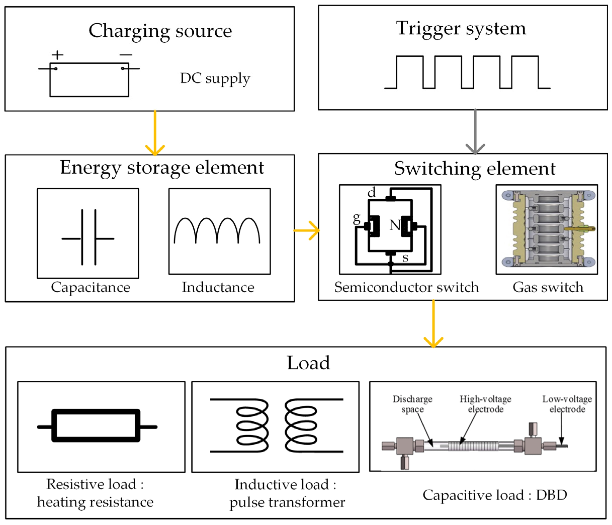
Pulsed power technology is a field of science and engineering dedicated to generating high-power pulses. This is achieved by rapidly storing and releasing high-density energy (typically in the microsecond to nanosecond range), effectively compressing and converting the primary energy source [1]. The basic topology of a typical pulsed power supply system, illustrated in Figure 1, comprises essential stages: energy storage, pulse formation, and switch control. The system operates by charging an energy storage element, which then quickly releases its stored energy to the load through a fast-switching component, generating a high-power pulse [2]. Recent progress in power electronics, thin-film dielectrics, and insulation has greatly broadened pulsed power applications. This expansion ranges from national defense and military applications, such as electromagnetic launchers (EML) [3] and directed energy weapons [4] and scientific research including Z-pinches [5] and plasma sources [6], to a diverse set of industrial and civilian sectors, such as sewage purification [7,8], food sterilization [9,10], and biomedicine [11,12]. Consequently, pulsed power technology is fostering a series of groundbreaking applications.
Although pulsed power technology offers extensive practical applications, its implementation encounters considerable obstacles. In sectors such as national defense and heavy industry, these systems must sustain reliable, long-term performance under challenging circumstances, including frequent discharge-recharge cycles and complex environmental factors. As such, reliability is essential for the successful operation of pulsed power systems. Neglecting this aspect can negatively affect the mean time between failures (MTBF) and result in increased maintenance expenditures as well as prolonged periods of system inactivity.
This challenge arises from the operational mode of slow energy storage and fast release, rather than any fundamental power limitation. Figure 2 reveals the interaction and coupling pathways of the electro-thermal–magnetic–mechanical stress fields within the pulsed power supply. The Joule heating effect and the Lorentz force, acting at the core of the components, serve as the respective hubs for electro-thermal and magnetic–mechanical coupling. These coupled effects trigger a series of cascading failure reactions, including dielectric breakdown, electrode erosion, thermal fatigue, and structural deformation, which collectively restrict the system’s overall reliability. Electrically, the high voltage rate dV/dt induces rapid changes in the electric field across the dielectric material, leading to a non-uniform electric field distribution. This results in localized energy concentration at dielectric interfaces and defect sites, where the transient electric field enhances displacement currents and initiates polarization dynamics that are out of equilibrium with the external field. These transient stresses give rise to thermal and electrical energy dissipation, which activate a series of physical processes, such as partial discharge, charge injection, and localized dielectric heating. Over time, this repeated energy injection causes microstructural damage, including the formation of Micropores, cracks, and space-charge accumulation. The cumulative effect of these degradation mechanisms induces critical parameter shifts, such as threshold voltage Vth drift, ultimately leading to dielectric breakdown or short-circuit failure. [16]. Thermally, high-repetition-rate pulsed operation inevitably induces thermal accumulation within the device. This sustained thermal cycling leads to excessive thermal stress, which subsequently promotes the formation of fatigue cracks on critical interfaces, such as the capacitor weld points and the switch surfaces [17]. Magnetically, the high electromagnetic forces inherent in the pulsed power supply leads to electrode surface erosion and morphological degradation. Importantly, when subjected to significant electromagnetic stress from high-voltage and high-current pulses, the contact resistance of the electrodes may exhibit substantial fluctuations, which can significantly undermine the overall stability of the system [18]. Mechanically, large mechanical stresses are inherently induced in certain demanding applications, such as electromagnetic ejection. This mechanical loading poses a direct threat to the structural integrity of the system, potentially resulting in deformation, structural failure, or fatigue damage [19]. The combined and interactive effects of these multi-physical factors elevate the reliability of the pulsed power supply to an interdisciplinary challenge. Addressing this issue necessitates a comprehensive analysis and the development of optimized design strategies spanning diverse fields, including electrical engineering, materials science, electromagnetics, and thermodynamics. Consequently, systematic research into the coupling mechanisms is paramount for achieving robust and sustainable pulse power system operation.
Currently, several significant research gaps remain in the reliability of pulsed power systems. For example, there is a lack of efficient, high-speed fault diagnosis and dynamic isolation methods at the system level. In addition, current modeling and prediction capabilities for structural and long-term cumulative fatigue effects are inadequate. Importantly, while coupled models for specific devices exist, there is currently no widely accepted system-level quantitative model that can comprehensively account for the complex interactions among the four main stresses—electric, thermal, magnetic, and mechanical. As a result, without a comprehensive database of power failures, it is not possible to establish an accurate operational lifetime model for these systems.
Given these challenges, improving pulsed power supply reliability is crucial for technological progress. This paper reviews recent studies, examining reliability issues and solutions from components to system integration and application scenarios. Its main aim is to outline a technical roadmap for developing durable, dependable pulsed power systems for stable, critical future uses.

2. Component Reliability

2.1. Energy Storage Elements

The core principle of pulsed power supply is the instantaneous release of energy stored over a significantly longer duration. Therefore, the features of the energy storage element are crucial because they essentially determine both the system’s highest possible output and the range of applications it can support [20]. More specifically, the energy density of the storage element establishes the theoretical upper bound on the total energy delivered per single pulse, while its power density simultaneously governs the achievable peak pulse power output of the system. Equivalent parameters such as the inductance Leq and resistance Req are crucial for shaping the output waveform, specifically by influencing the pulse width and the rising edge [21]. Furthermore, the charging frequency and efficiency directly govern the output repetition rate, while the energy density of the system imposes a direct constraint on the overall power supply volume and weight. However, under long-term, repetitive pulsed operation, the accumulation of electro-thermal stress causes the gradual degradation of the storage element’s dielectric properties and internal structure. This degradation directly results in the drift of key performance parameters, which consequently manifests as output energy attenuation, waveform distortion, and a decline in system efficiency. Ultimately, this process causes the actual power supply performance to severely deviate from the initial design specifications [22]. Therefore, thoroughly investigating the reliability of energy storage components is essential to ensure the stable, long-term operation of pulsed power systems.
Table 1 outlines pulsed power system classifications by energy storage type, followed by a detailed description of each.

2.1.1. Capacitive Storage

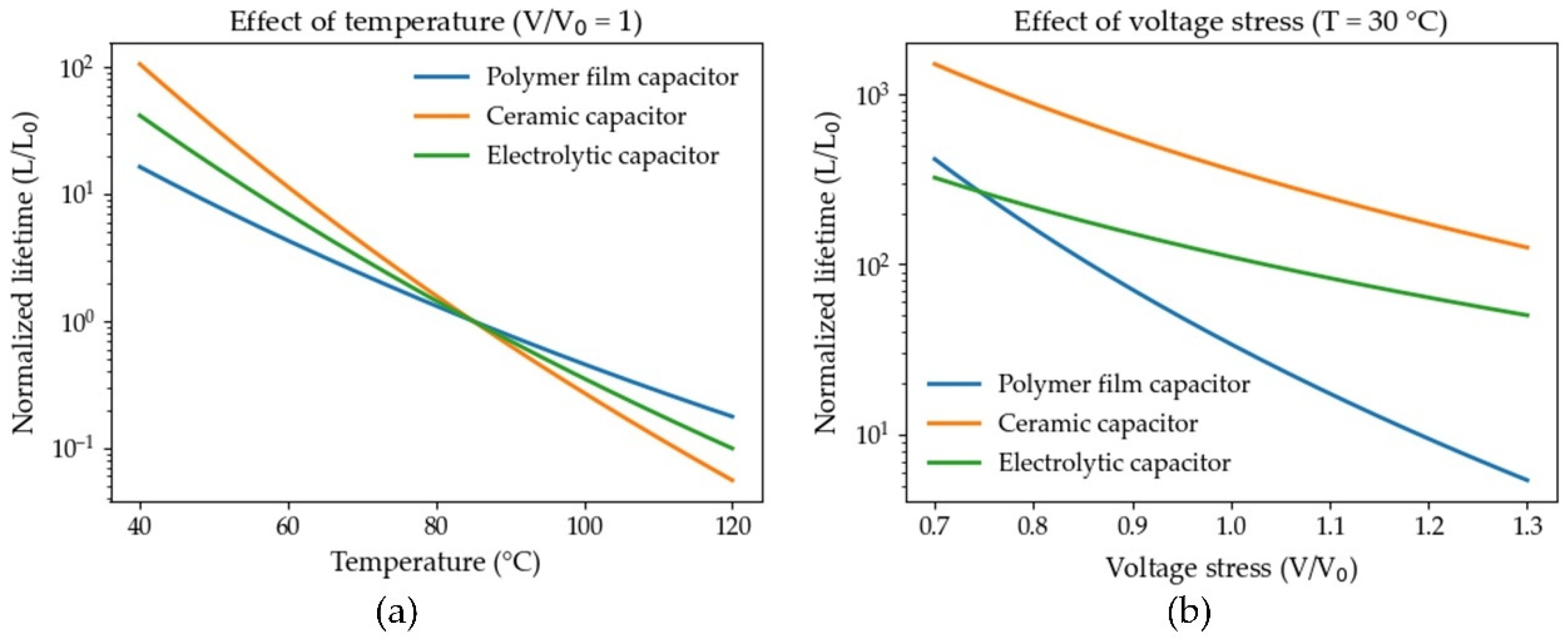
Persistent electro-thermal stress is inevitable during long-term repetitive pulsed operation. This sustained stress drives the gradual aging of the energy storage capacitor’s dielectric material, resulting in the weakening of its internal polarization mechanism. Studies of the microstructure and overall electrothermal performance reveal that changes in the electrical structure of energy storage capacitors are not just due to cumulative channel damage or localized breakdowns caused by nanosecond, high-intensity pulses. These changes are also influenced by the combined effects of rising internal temperatures and distortions in the local electric field, both of which result from operations at high repetition rates [22,31]. The most widely used empirical model for capacitors is given by (1), which describes the influence of temperature and voltage stress.
L = L 0 × V V 0 n × exp E a K B 1 T 1 T 0
where L and L0 are the lifetime under the use condition and testing condition, respectively. V and V0 are the voltage at use condition and test condition, respectively. T and T0 are the temperature in Kelvin at use condition and test condition, respectively. Ea is the activation energy, KB is Boltzmann’s constant (8.62 × 10⁻⁵ eV/K), and n is the voltage stress exponent. Therefore, the values of Ea and n are the key parameters to be determined in the above model [32]. Due to variations in dielectric materials and failure mechanisms, the values of Ea and n differ significantly across capacitor types. For electrolytic capacitors, Ea typically ranges from 0.6 to 0.95 eV, with n approximately 3–5 [33]. In contrast, polymer film capacitors exhibit Ea values of 0.4–1.5 eV and n values of 5–9 [34]. while ceramic capacitors demonstrate Ea in the range of 0.8–1.5 eV and n between 2 and 6 [35]. Based on (1), Figure 3a,b illustrates the variation trends of capacitor lifetime with respect to temperature and voltage stress, respectively. These plots demonstrate that the lifetime exhibits a strong non-linear sensitivity to operating conditions.
Furthermore, under pulsed conditions, each type of energy storage capacitor exhibits unique failure mechanisms, such as dielectric aging in ceramic capacitors, electrical breakdown in polymer film capacitors, and electrolyte dry-out in electrolytic capacitors. Although these mechanisms depend on the specific material, Table 2 highlights their shared foundation: changes in microstructure and declines in performance caused by the combined impact of electro-thermal stress and charge injection. Parameter drifts, influenced by differing media characteristics and architectural aspects of the storage element, can result in substantial deviations of the power output’s energy and waveform from intended specifications. As a result, such drift constitutes a significant constraint on both the reliability and operational longevity of the pulsed power system.
Researchers, addressing the failure mechanisms of energy storage capacitors under pulsed conditions, have recently focused on mitigation strategies such as material modification, structural innovation, and system-level management to improve reliability, lifespan, and performance. As the energy density and repetition frequency of pulsed power systems continue to advance, the inherent limitations of traditional energy storage capacitors—specifically regarding dielectric strength, thermal shock resistance, and operational lifetime—have become increasingly acute. This situation has served as a major impetus for the accelerated development of novel dielectric materials.
The energy storage capacitor is often the main reliability limitation in pulsed power supplies due to its restricted dielectric strength, poor thermal shock resistance, and reduced lifespan under high energy and frequent use. Researchers have developed a multi-level reliability framework that innovates in material properties, internal structure, and packaging. Enhancing material properties aims to improve dielectric thermal stability and functionality, meeting stricter requirements for high-temperature and high-frequency use. For polymer film capacitors, traditional biaxially oriented polypropylene (BOPP) has been progressively substituted by polymers possessing superior glass transition temperatures and exceptional thermal stability, such as polyethylene terephthalate (PET), polyethylene naphthalene (PEN), and even advanced materials like polyphenylene sulfide (PPS) and polyether ether ketone (PEEK). These novel material systems ensure stable dielectric strength and energy density in environments up to 150–250 °C [44,45]. Furthermore, the introduction of inorganic nano-fillers with high dielectric constants, such as BaTiO3, Al2O3, and BN, via nanocomposite technology to form functional composite films, has yielded multiple benefits [46,47]. This not only enhances the dielectric’s overall polarization energy storage capacity but also significantly reduces its sensitivity to partial discharge and improves breakdown resistance at the dielectric mechanism level.
Reliability for ceramic capacitors centers on improving grain boundaries and DC bias performance. Researchers have successfully mitigated oxygen vacancy migration and grain boundary charge accumulation through fine element doping Zr, Mn and texturing techniques [48,49]. This suppression is vital for slowing aging and maintaining capacitance stability under high direct current bias, thereby greatly extending the effective device lifetime.
Significant improvements in the reliability of electrolytic capacitors depend on creating innovative electrolyte systems [50,51]. These new electrolytes effectively inhibit the evaporation and gasification of conventional electrolytes under high temperature and pulsed conditions. The resulting benefits include a significant reduction in equivalent series resistance (ESR), broader operating temperature ranges, and substantially improved capacitor pulse durability.
Beyond intrinsic material innovation, the internal structure and packaging technology of the capacitor also play a pivotal role in determining overall system performance. At the structural level, optimizing the stacking or winding configuration aims to reduce the effective current loop area. This is a key approach to minimizing equivalent series inductance (ESL) and inductive coupling [52,53]. Concurrently, the internal electrode connection method is being upgraded from traditional spot welding to ultrasonic welding or more refined contact architectures. The objective is to reduce contact resistance, enhance the mechanical and electrical stability of the connection, and minimize localized heat loss [54].
High-reliability packaging materials and designs, including flame-retardant epoxy resins, ceramics, and metal enclosures, protect internal components against humidity, vibration, and extreme temperatures. This reduces risks like moisture absorption, electrode corrosion, and mechanical fatigue [55,56,57].
During high-repetition-rate, large-current pulsed operation, energy storage capacitor failure is mainly caused by electro-thermal coupling stress. As shown in Figure 4, the process begins with rapid dV/dt and overvoltage, leading to electric field distortion and charge injection. Continued energy dissipation and rising temperatures accelerate electrode migration, dielectric carbonization, and terminal corrosion, resulting in reduced capacitance, increased ESR, and ultimately diminished output energy and waveform distortion of the power module [58,59].
Additionally, to achieve higher energy storage capacity, capacitors in pulsed power supplies are typically deployed in cascaded configurations, particularly in Marx generators and pulse forming network (PFN). In energy storage modules comprising multiple capacitors connected in series and parallel, a single-point failure has the potential to trigger a severe cascading failure. In a series branch, a short-circuit failure effectively bypasses the faulty capacitor. Consequently, the total branch voltage is redistributed across the remaining intact capacitors, subjecting them to voltage stresses exceeding their rated limits. Without a rapid voltage balancing mechanism, this leads to sequential breakdown due to overvoltage. Conversely, in a parallel group, a shorted capacitor creates an extremely low-impedance path. This causes adjacent healthy capacitors to discharge rapidly through this path within microseconds or even nanoseconds. The resulting transient current generates excessive electromagnetic forces and Joule heating, potentially damaging the electrode connections or internal structures of neighboring components [60,61]. Furthermore, localized heating from the failed unit propagates via thermal conduction, accelerating dielectric aging or inducing direct thermal breakdown in adjacent capacitors, thereby initiating a positive feedback loop of thermal runaway.
To effectively mitigate this degradation from the source, a dual, parallel strategy is typically employed. On the one hand, at the topology level, multi-level and soft-charging control strategies are implemented to constrain the peak dV/dt and charging stress on individual capacitors. Furthermore, cross-cell voltage equalization and redundant bypass are realized via equalization circuits to minimize the impact of single-point failures on the module [62,63]. On the other hand, the operational level focuses on online monitoring. This is achieved by implementing real-time estimation of capacitance, ESR, and leakage current, coupled with an electro-thermal degradation model, which supports residual life estimation and predictive maintenance decisions [64,65,66]. The synergistic linkage between these topology and online prediction strategies allows for a significant extension of the capacitor module’s operational lifetime and a reduction in unexpected downtime risk, all without substantially compromising power density.

2.1.2. Inductive Storage

In pulsed power supplies, inductive energy storage offers a significantly higher energy density compared to capacitive storage, making it particularly suitable for storing enormous energy above the megajoule level [21]. Furthermore, pulsed power systems based on inductive storage can typically achieve ultra-high transient response and extremely fast current rise rates (di/dt) using magnetic or semiconductor switches. This capability makes it irreplaceable in applications requiring instantaneous large current shocks, such as driving particle accelerators, high-energy lasers, or electromagnetic emission systems [67,68].
The combination of high energy density and high di/dt in inductive energy storage creates significant reliability challenges. During pulse discharge, coils face intense mechanical stress from Lorentz forces [69,70], while high di/dt causes eddy current losses and transient voltages that speed up insulation aging [71]. These stresses reduce pulsed power supply reliability over time. Additionally, switching elements must handle sudden turn-off under high current, with transient voltage dominated by L · di/dt, placing strict demands on switch design [72]. Thus, the overall reliability of the system heavily depends on the switch’s performance.

2.1.3. Flywheel Energy Storage

In a Flywheel Energy Storage System (FESS), electrical energy is converted to kinetic energy and stored by spinning a flywheel at high speeds. FESS operates in three main modes: charging, discharging, and holding. During charging, the flywheel rotor absorbs external energy, storing it as kinetic energy while accelerating to a set speed. In discharging mode, generators draw kinetic energy from the flywheel rotor, convert it back to electrical energy, and supply current and voltage to electrical devices with the help of power control systems. As the flywheel releases energy, it slows down until it reaches a specified minimum speed. In holding mode, once the flywheel reaches its target speed, it neither gains nor loses energy; if energy losses are ignored, its energy remains unchanged. These modes allow the flywheel system to efficiently control energy input, output, and storage [73].
Flywheel Energy Storage is well-suited for pulse generators due to its high-power density, fast response capability, longevity, and high efficiency [74,75]. It can continuously absorb low-power input from the grid and release enormous energy (MJ-level) to the generator load within a very short duration, thereby significantly enhancing the system’s instantaneous power output capacity [76]. However, achieving high- power density necessitates extremely high-speed operation, which generates immense centrifugal forces. This, in turn, causes complex resonance and fatigue accumulation among the flywheel rotor, bearings, and stator [77], accelerating the mechanical wear of the assembly and amplifying material defects in any part, which may ultimately result in catastrophic failure [29].

2.2. Switching Elements

The switching element regulates energy flow from storage to load, determining when and how much energy is released. Its performance parameters are decisive in determining the quality of the output pulse and the upper limit of the overall system capacity in pulsed power systems, this energy involves high voltage and large currents, so the switch must endure significant electro-thermal stress. Its failures are often sudden and severe, making reliability crucial for stable system operation [78,79].
Switching elements in pulsed power systems fall into three main categories based on their technical principles: mechanical, semiconductor, and plasma switches [80]. Table 3 outlines the specific failure mechanisms corresponding to each of the three categories, followed by a comprehensive explanation for each.

2.2.1. Gas Spark Gap Switch

The failure mechanism in gas spark gap switches is predominantly derived from the synergistic effect of multiple physical and chemical processes. Firstly, during each discharge event, the combination of high current density and short-duration thermal input causes partial melting or vaporization of the electrode surface. This action results in electrode mass loss, noticeable melting traces, and material erosion. This entire process is intricately linked to the electrode material’s thermophysical properties (such as thermal conductivity, melting point, and specific heat) and the single-pulse transferred charge [81].
Secondly, with the accumulation of multiple discharges, structural damage—including cracks, pitting, bulges, and splash spheres—gradually develops on the electrode surface. These formations do not only increase the electrode roughness but also concentrate the local electric field, thereby aggravating partial discharge or premature breakdown [89].
Thirdly, particle sputtering and migration between electrodes, with subsequent deposition in the gap or on walls, contaminate the insulation path and create localized conductive channels. This process undermines the stability and reliability of the self-breakdown voltage VSB [90].
Ultimately, these physical and chemical effects degrade key switch parameters, causing instability or reduction in VSB, lower trigger reliability, and eventual switch failure after repeated cycles.
Prolonged, repetitive pulse discharge affects the reliability of gas spark gap switches primarily because of electrode damage caused by intense high current, high voltage, and frequent switching. The main failure arises when the electrode material melts and vaporizes, which leads to particle splashing and deposition. To address these issues, research has progressed from modeling and analyzing fundamental damage mechanisms to optimizing electrode materials and structural design. In exploring these mechanisms, researchers have used detailed numerical models to better understand how material is removed during operation.
The volume of fluid (VOF) method is used to construct a multiphase flow removal numerical model and compare it with the experimental data. The results show that reducing the wear caused by melting or vaporization can be achieved by two main ways: one is to increase the polar pressure drop, and the other is to select materials with better thermal properties, thereby extending the effective working life of the switch [91].
Based on the understanding of the mechanism, the improvement of the material system has become the key to improving the durability of the switch. Researchers have carried out a wide range of pulse discharge experiments on various high-performance alloy electrodes, such as high-pulse current discharge tests on alloy electrodes such as W-Ni-Fe and W-Cu. By measuring their surface morphology and erosion degree, it is clear that material alloying and microstructure control are strategic methods to effectively reduce melting and vaporization damage [92].
The structural design of the electrode has a critical influence on the dispersion and concentration of thermal stress. Studies show that optimizing the electrode geometry alongside appropriate material selection can significantly mitigate thermal stress concentration, thereby minimizing localized damage and ensuring the switch’s long-term stable operation [93]. Long-term reliability depends not just on initial design, but also on operational conditions and maintenance. Analysis under conditions like 0.3 MPa pressure, 30 Hz repetition rate, 8.5 kA peak current, and −35 kV voltage shows electrode spatter affects switch lifespan. Using materials prone to less spatter and regular maintenance can extend switch life [94].
Periodic electrode replacement is considered a feasible strategy to extend the switch’s operational lifetime. To prevent or minimize thermal damage to the new electrode during this process, theoretical studies leveraging the Holm model, Hertz formula, and heat conduction theory have demonstrated that manufacturing electrode brackets from metals or alloys with superior thermal resilience or those incorporating trace amounts of rare earth elements can effectively mitigate replacement-induced thermal damage [95].
Ultimately, the dynamic assessment of the switch’s internal environment offers crucial theoretical support. By applying the Joule heat accumulation method to analyze the resistance characteristics of the spark channel, research revealed the pressure and temperature evolution law within the switch chamber: this typically features an initial rapid growth, followed by a slower increase, and ultimately stabilizing. Notably, the increase in pulse current amplitude significantly enhances heat deposition. This understanding provides a vital thermal management theoretical basis for designing highly reliable, long-life gas spark gap switches [96,97].

2.2.2. Wide Bandgap Semiconductor Switch

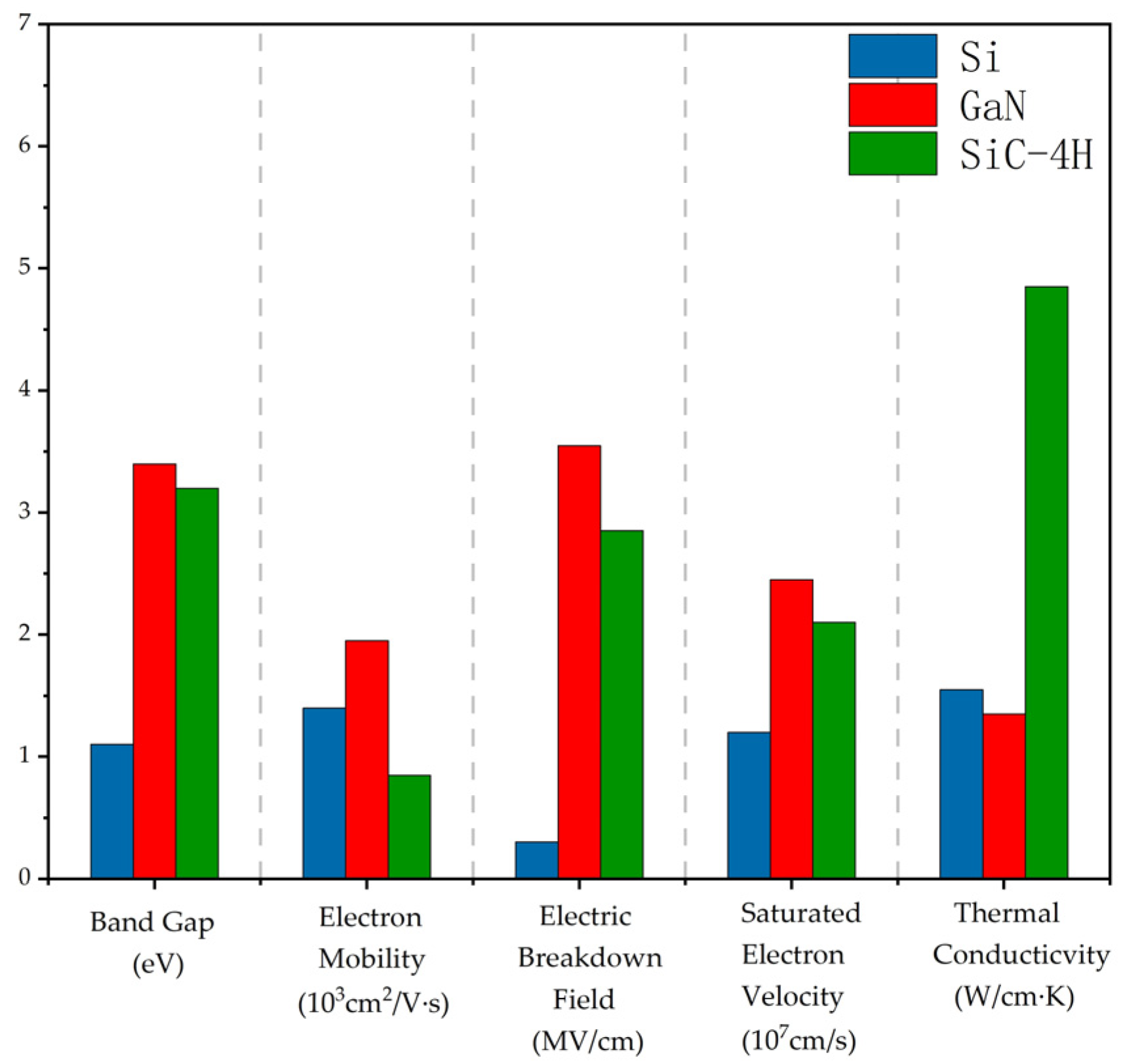
Silicon-based devices have traditionally dominated the field of semiconductor switching technology. However, their lower bandgap, limited breakdown electric field, and restricted carrier mobility impose fundamental constraints that increasingly hinder advancements in power density and efficiency for pulsed power systems [98]. Wide-bandgap (WBG) semiconductor materials, specifically SiC and GaN present a robust solution to these limitations, owing to their superior intrinsic properties. As depicted in Figure 5 both SiC and GaN demonstrate significant advantages over conventional silicon in several critical material parameters: their larger bandgaps support stable operation at elevated temperatures; higher breakdown electric fields allow for more compact device architectures and improved voltage blocking capabilities; and enhanced electron saturation velocity and thermal conductivity facilitate rapid switching and effective heat dissipation. These characteristics collectively result in greater power density, minimized switching losses, and improved resilience to severe electro-thermal stress in switching devices [99]. Therefore, the following section will focus on the reliability aspects of WBG semiconductor switches.
Wide-bandgap semiconductor switches are widely adopted in pulsed power supply applications due to their high switching speeds, precise controllability, and extended operational lifespans. Nevertheless, their reliability under strenuous electro-thermal-mechanical multi-field conditions remains a critical limiting factor in overall system performance. Comprehensive reliability analysis of these semiconductor devices is essential for advancing pulsed power technologies. The varied failure mechanisms observed in these switches primarily originate from uncontrolled energy dynamics and material degradation, driven by the interactions across extreme electro-thermal-mechanical fields.
Firstly, electrical overstress represents the primary threat: when the switch is rapidly turned off, the circuit’s parasitic inductance generates an induced voltage. This induced voltage superimposes onto the direct current bus voltage, resulting in a transient overvoltage that significantly exceeds the device’s rated value and subsequently leads to localized or complete device failure. In the case of MOSFETs, this failure mode is typically initiated by the device entering an avalanche state [86,100].
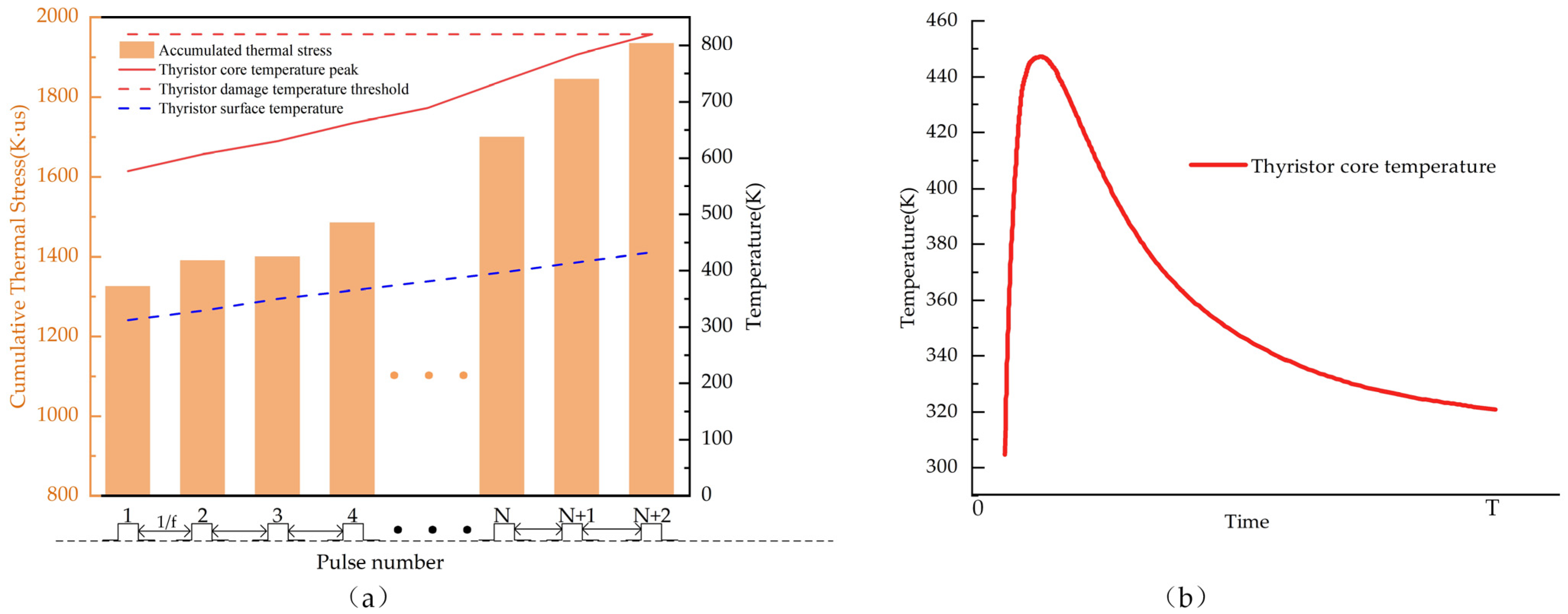
Secondly, thermal failure is often triggered by electrical overstress: excessive electrical stress intensifies the thermal effect, which subsequently affects the device’s internal material structure and current distribution. This process causes the current carrying capability to concentrate locally, leading to the formation of a ‘hot spot’. As illustrated in Figure 6, within a repetitive pulse sequence, each pulse induces a transient temperature spike at the device’s core. This initiates a positive thermal runaway feedback loop in the affected region: increased temperature reduces resistance, which elevates the carrier concentration, thereby boosting the current flow. This vicious cycle ultimately leads to device destruction via fusing or secondary breakdown [101,102]. Cyclic thermal stress gradually degrades the interlayer dielectric, which can lead to source metallization melting and a partial short-circuit between the gate and source. The fatigue life associated with this thermal failure mechanism typically follows the Coffin–Manson model [103]. The relationship between the number of thermal cycles and device failure under various electro-thermal stresses is expressed by (2) [104].
N f = K Δ T j β 1 e β 2 T j m i n + 273 t o n β 3 I β 4
where Nf is the number of cycles to failure, ton is the duration of the device on time during each cycle, ΔTj is the junction temperatures swing, Tj-min is the minimum temperature of the device, and I is the current per bond wire. The model parameters K and β1-β4 are determined by least squares curve fitting of the test data.
In summary, the synergistic coupling of electro-thermal-mechanical stresses leads to physical failure modes categorized into two distinct dimensions: chip-level and package-level [106]. At the chip level, degradation primarily manifests as gate oxide failure and body diode failure. Specifically, gate oxide failures are typically induced by electrical overstress and high temperatures, which trigger interfacial charge accumulation or dielectric breakdown. Conversely, body diode failures predominantly stem from forward voltage bias stress [107]. To quantify these degradation mechanisms, the key parametric indicators include the threshold voltage (Vth), on-state resistance (RDson), critical avalanche energy (EAV), and gate leakage current (IGSS). The threshold voltage (Vth) instability is a complex phenomenon primarily driven by bias temperature instability (BTI) and charge trapping in the gate oxide. Two distinct failure modes arise from this instability: A negative drift, typically induced by hole trapping, is critical as it erodes the noise margin. Once the threshold drops below a safety limit, it can trigger spurious turn-on events and catastrophic shoot-through. Conversely, a positive drift induced by electron trapping increases the on-state resistance (RDSon) by reducing the effective overdrive voltage, thereby degrading switching speed and increasing conduction losses [108,109]. Functionally, a failure is defined when the on-state resistance increases by 15% [104]. Furthermore, monitoring the magnitude of the gate leakage current (IGSS) serves as a robust method for failure detection. Under healthy operating conditions, IGSS typically remains in the nano-ampere (nA) range; however, upon device failure, this current can escalate drastically to the milli-ampere (mA) level. Moreover, driven by cumulative physical degradation, the evolution of IGSS is often non-linear. The onset of an exponential growth pattern in leakage current is widely identified as a critical precursor to device failure [103]. In terms of energy tolerance, the critical avalanche energy (EAV) defines the device’s thermodynamic limit. When the dissipated avalanche energy causes the junction temperature to exceed the melting point of the source metallization (such as Aluminum), it operates outside its safe operating area (SOA). This thermal breakthrough serves as a deterministic criterion for catastrophic avalanche failure [110,111].
Common package-level failures predominantly comprise bond-wire lift-off and solder layer fatigue. The critical parameters for characterizing these degradation processes are the on-state voltage (VDson) and the thermal impedance (Zth) between the chip and the copper substrate. According to the AQG 324 guideline, the failure criteria are explicitly defined: a device is deemed to have reached its end-of-life (EOL) when the on-state voltage increases by more than 5% relative to its initial value, or when the thermal impedance rises by 20% [112].
To effectively mitigate the failures arising from electro-thermal field coupling in pulsed environments, researchers have developed and substantiated a broad spectrum of strategies.
Firstly, in terms of device process and structure optimization, the core objective is to enhance the durability and avalanche tolerance of the gate dielectric. By establishing a unit-level behavior model for short-circuit and avalanche breakdown faults, researchers can clearly describe the thermal failure progression of these two events. This enables designers to intuitively and rapidly evaluate and improve device characteristics, thereby identifying weak links at the design origin [113]. Reliability assessments of gate oxide layers; mainly conducted via precise time-dependent dielectric breakdown (TDDB) tests highlight how the lifetimes of various MOSFET structures, such as planar and asymmetric trench designs, depend on electric field stress from bias. For example, planar oxides demonstrate superior lifespans when subjected to negative bias, whereas trench oxides perform better under positive bias [114]. Moreover, innovative device architectures greatly enhance overall performance. A newly developed deep trench sub-gate super-junction 4H-SiC MOSFET offers reduced specific on-resistance and switching loss while preserving high breakdown voltages by eliminating complicated multi-epitaxial processes [115]. Additionally, the SiC dual-channel MOSFET, featuring a lower-barrier diode and an L-shaped gate-source embedded in the gate trench, efficiently suppresses body diode reverse conduction. Its split gate design enables faster switching speeds, surpassing conventional structures in both voltage drop and switching performance [116].
Secondly, research at the chip and packaging levels focuses on reducing parasitic inductance and improving thermal management, which are fundamental ways to manage transient overshoot and thermal stress. Novel discrete device packaging, such as structures employing stepped etching active metal brazed substrates and flexible printed circuits, achieves a seamless combination of high thermal conductivity, full electrical isolation, and low stray inductance, significantly enhancing the SiC MOSFET’s electrical performance [113]. Innovative ultra-high thermal reliability embedded liquid-cooled SiC 3D packaging structures, achieved by stacking embedded micro-pin fin SiC substrates on copper cold plate manifolds, demonstrate superior thermal stability, heat dissipation efficiency, and temperature uniformity over traditional DBC substrate SiC power modules [117]. In connection technology, laser micro-welding has been implemented for bonding the source contact of Ag-sintered, copper-bonded top plate-enhanced SiC MOSFETs. This method demonstrates reduced sensitivity to surface properties and improved reliability when compared to conventional ultrasonic copper wire bonding techniques [118].
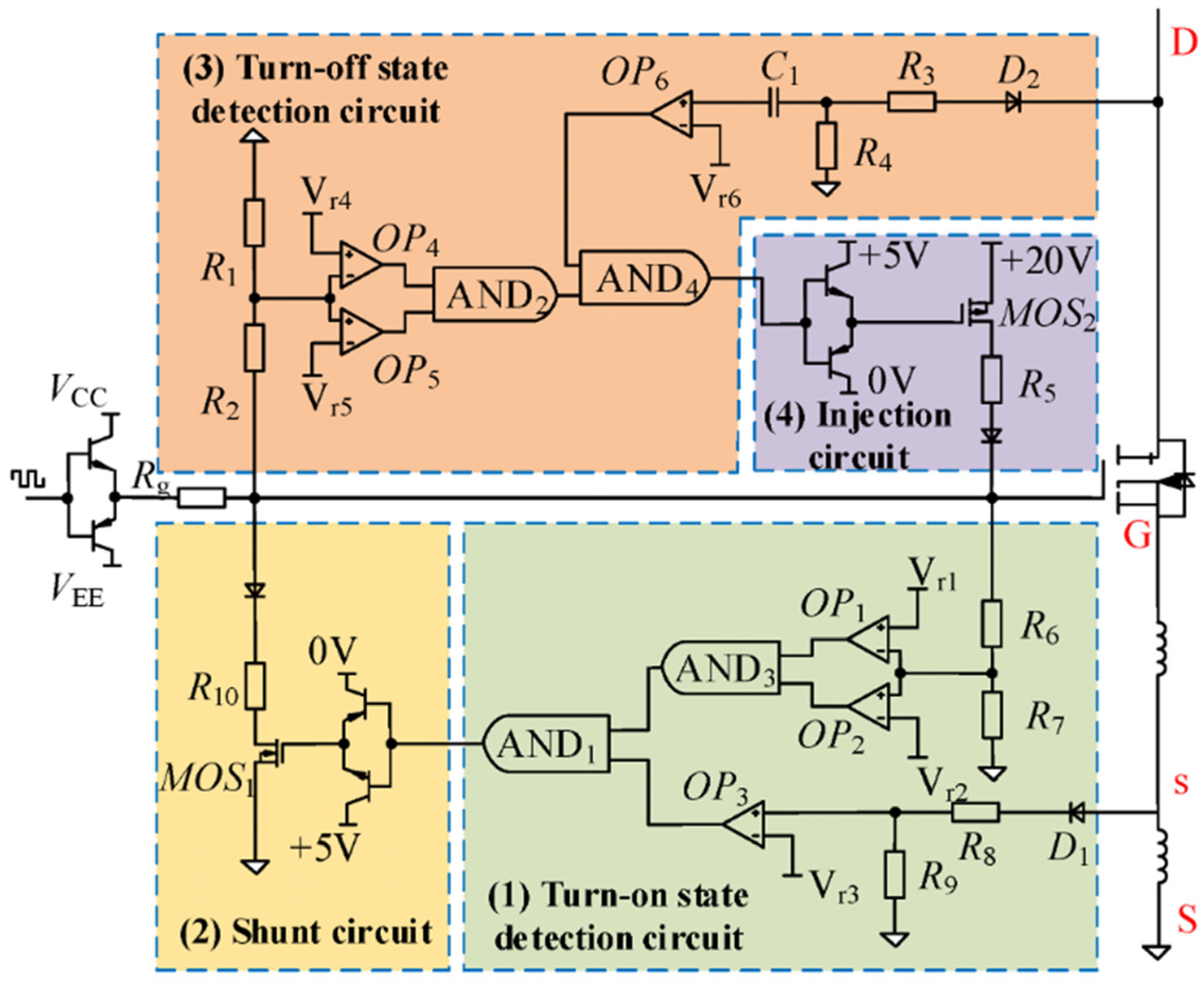
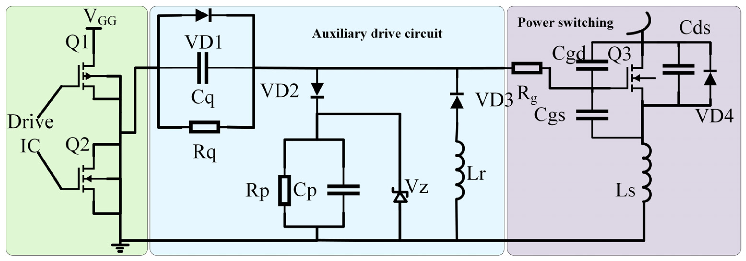
Thirdly, optimizing the gate drive and controlling dV/dt are effective in suppressing spurious turn-on due to Miller coupling and reducing turn-off overshoot. Gate drive design has formed two primary optimization strategies. The first is the active intelligent control scheme, which utilizes detection and feedback loops to achieve accurate dynamic control over the switching transient. The dV/dt control method in the active gate driver (AGD), for instance, actively modulates the turn-off gate resistance to realize voltage balancing in stacked devices during the turn-off transient [119]. This method is further refined by using digital open-loop control AGD [120] or by introducing negative feed-back [121], aiming to suppress inrush voltage and shorten the switching transient time. Another AGD variant, the IS-AGD (independent suppression AGD) [122], focuses on optimizing the switching trajectory through independent suppression of overshoot and oscillation, achieving finer control. As illustrated in Figure 7 [123], the circuit utilizes a resistive divider network (R1, R2, R6, R7) to sense the switching status. Subsequently, the comparators (OP3, OP6) and logic gates (AND1–4) accurately determine the optimal timing for active intervention. Based on these logic outputs, the auxiliary MOSFETs (MOS1, MOS2) are activated to regulate the gate current through shunting or injection. This specific configuration allows for a significant reduction in electromagnetic interference (EMI), with experimental data showing a decrease in current and voltage overshoots of 39–53% and 48–54%, respectively, while maintaining the original switching speed. The second strategy explores more concise and efficient Passive Resonance Assistance schemes. This approach avoids complex active components, inherently lowering drive circuit complexity and cost. A typical example, the resonant auxiliary drive circuit shown in Figure 8, the capacitor Cq and inductor Lr placed between the gate and the source constitute a resonant loop. Simultaneously, Rp, Rq, Cp, and Cq constitute a voltage division network, while VD1, VD2, VD3, and VDZ function as a voltage clamping mechanism. This ingeniously achieves a smooth, zero-voltage transition of the gate voltage during the turn-off period. The resulting mechanism not only effectively suppresses bidirectional crosstalk but also yields faster switching speeds and lower switching losses [124]. Thus, these passive schemes prioritize topological simplicity and efficiency alongside high performance.
Finally, the absorption and energy feedback circuit is adopted, with the optimized layout or design, to reduce the overvoltage caused by parasitic inductance and improve the single pulse avalanche and transient tolerance of the device. For example, researchers have proposed a SiC MOSFET overvoltage and oscillation suppression circuit (OVSC) that integrates switching loss optimization and clamping energy feedback characteristics. The circuit not only achieves excellent suppression performance for overvoltage and oscillation, but also significantly reduces the switching loss of the device by cleverly using clamping capacitors and mode-locked capacitors, achieving the unity of performance and efficiency [125]. At the same time, in-depth theoretical analysis also provides the basis for the design of the buffer circuit. By establishing the research model of the parasitic parameters of the device, the parameters of the buffer component are accurately selected and the circuit performance is optimized [126,127].

2.2.3. Photoconductive Switch

Photoconductive Switches (PCSS), as a representative solid-state switch, are widely employed in pulsed power systems, owing to their ultra-fast response, low jitter, and high peak current capability. However, despite these advantages, PCSS is less prevalent than other switch categories, and its practical application is limited by numerous coupling failure paths [85]. Specifically, the device is prone to forming self-sustaining avalanches and hot spot current channels under the challenging conditions of high electric field and low optical excitation. Furthermore, instantaneous, concentrated energy injection can induce irreversible electrode damage [128]. Moreover, the high current density resulting from light triggering generates significant Joule heating. The inability to dissipate this heat quickly leads to localized melting and material denaturation. Furthermore, uneven or excessive optical excitation accelerates cumulative damage, consequently limiting the device lifetime [129,130]. In summation, the failure of the PCSS is a complex electro-optical-thermal multi-field coupling process, characterized by both transient, catastrophic breakdown and long-term cumulative degradation.
Researchers have developed a multi-dimensional optimization framework to improve PCSS performance and reliability by controlling electrode contact, internal electric fields, and external triggers.
The primary objective is to ensure efficient current injection and extraction while suppressing surface failure under high fields. Studies confirm a competitive interplay between PCSS surface flashover breakdown and bulk current channel formation. Analysis of back-illuminated trigger electrode structures provides a vital empirical basis for optimizing electrode geometry and layout to mitigate surface electric field concentration [131]. For achieving high-performance ohmic contact in WBG systems, advanced techniques are paramount. In AlGaN/GaN structures, forming a good ohmic contact to the high-concentration two-dimensional electron gas (2DEG); produced by spontaneous and piezoelectric polarization, is achieved through metal deposition and annealing, which improves peak current and device reliability [130]. Moreover, research suggests fundamentally improving ohmic contact quality by filling the electrode–substrate gap with a 100 nm p-type epitaxial layer and Ti/Pt/Au metal electrodes [132].
The core objective in device structure and electric field regulation is to optimize the internal E-field distribution to enhance the switch’s voltage withstand capability. Researchers introduced a design strategy utilizing a low resistance region (LRR) structure to modulate the PCSS electric field and mitigate local peak E-field concentration. This method successfully improves the device’s breakdown voltage under high fields without compromising the light absorption area or increasing the on-state resistance [133]. Furthermore, analysis of the trigger position revealed the structure’s sensitivity to conduction performance, showing that cathode triggering achieves a shorter delay time and lower on-resistance compared to anode triggering under identical conditions. This provides a clear strategic direction for subsequent trigger mechanism and structure optimization [134].
In terms of external triggers, expanding the trigger region width facilitates rapid carrier density multiplication and the formation of avalanche ionization domains. Consequently, this shortens the PCSS delay and switching times, effectively minimizing trigger jitter [135].

2.3. Impact of Component Reliability on System Performance

The reliability of energy storage and switching elements within pulsed power systems is interconnected, as each component’s performance affects the others. The overall system output depends heavily on the reliability of individual elements. For example, changes in the parameters of the energy storage capacitor impact both the pulse energy and the waveform delivered to the load. At the same time, deterioration in the switching device can further disrupt the pulse waveform and compromise timing accuracy [136,137]. When both components degrade together, the system’s output may significantly stray from its intended design specifications. Therefore, future designs for individual devices must incorporate sufficient safety margins to ensure that a localized failure does not propagate to other system components.

3. System Integration Reliability

Studies show that even if each part is designed for maximum performance, the whole system may still fall short of its required reliability standards. Having reliable components is only one piece of the puzzle but it doesn’t guarantee the entire system will work as intended. When these components interact after being put together, new potential failures can arise, holding back overall effectiveness. Therefore, to truly improve reliability in pulsed power supplies, it is essential to shift focus from just individual parts to the entire system, using structured approaches for designing, evaluating, and managing reliability.

3.1. System-Level Thermal Management

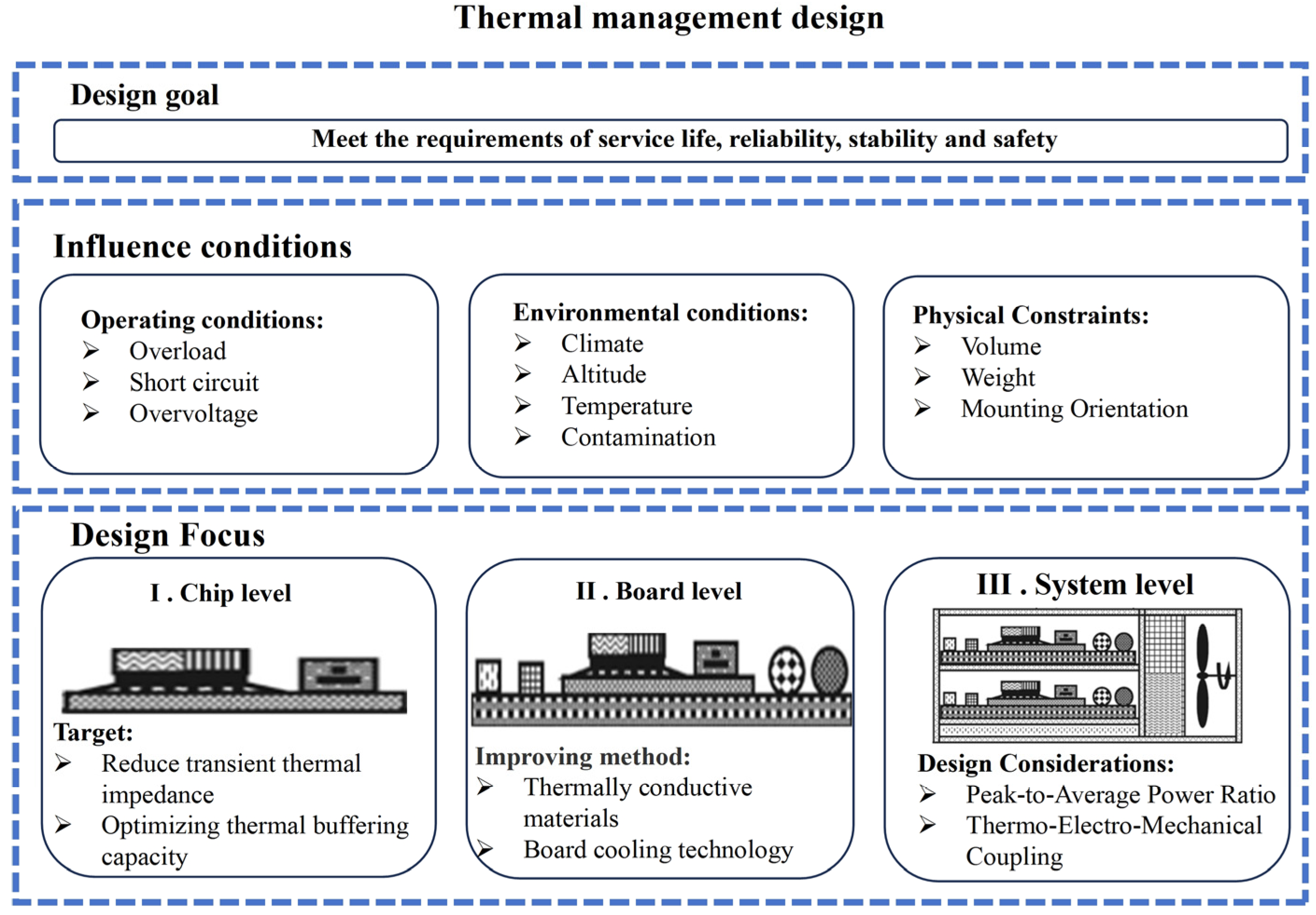
As illustrated in Figure 1, the fundamental unit of the pulsed power module comprises a charging power supply, an energy storage element, a switching element, and a load. The system realizes slow energy storage and rapid discharge through the modulation of the switch, typically resulting in the output of an instantaneous high-power square wave. However, this high instantaneous power inherently generates significant energy losses, such as switching losses and ESR losses within the capacitor [38]. These losses inevitably accumulate as heat within the energy storage and switching components. Ultimately, component failure is induced, which consequently precipitates the failure of the entire pulsed power supply. As illustrated in Figure 9, thermal management design must be integrated across all hierarchical levels of the power supply system. By implementing a rational combination of component-level, board-level, and system-level thermal design, the complexity of the cooling system is reduced, and the overall heat dissipation effectiveness is significantly enhanced. At the component level, the design objective is to efficiently extract heat from the power chip core to the package housing via high-performance thermal interface materials (TIMs). At the board level, the focus shifts to employing effective cooling technologies to address multi-chip layouts and complex thermal coupling effects. At the system level, a final cooling design must be chosen with careful attention to electro-mechanical integration. The thermal system is shaped by environmental conditions and the system’s operating profile, aiming to meet safety, reliability, and longevity requirements throughout its lifecycle.
Cooling technologies are broadly categorized into four main methods: air cooling, solid-state cooling, single-phase liquid cooling, and phase-change cooling [139]. From a thermal engineering perspective, the objective of the cooling system is to minimize the total thermal resistance Rconv from the junction to the ambient environment. The convective thermal resistance is governed by Newton’s Law of Cooling, as shown in (3).
q = h A ( T s T )
where q denotes the heat flux, h represents the heat transfer coefficient, A is the effective heat transfer area, Ts is the surface temperature, T refers to the ambient fluid temperature. The definition of thermal resistance is provided in (5). Consequently, as derived in (4), the thermal resistance is inversely proportional to the heat transfer coefficient and the effective heat transfer area [140].
R c o n v = T s T q
R c o n v = 1 h A
Equations (3)–(5) govern the fundamental heat rejection mechanism for fluid-based systems. Although Solid-state cooling operates via active conduction mechanics, its system-level performance is ultimately constrained by the convective heat rejection efficiency at its hot side. Consequently, maximizing h or A remains the universal design goal.
Air cooling typically involves adding fans to heat-generating components or the entire assembly for temperature reduction, or employing advanced dual-piezoelectric cooling jets (DCJ), which disturb the boundary layer over thermal elements to enhance heat dissipation [141].
Solid-state cooling encompasses thermal conduction techniques and thermoelectric cooling technology (TECT). Thermal conduction technologies rely on conduction mechanisms to enhance heat transfer efficiency by expanding the contact surface area between the semiconductor casing and the cooling medium [142]. Thermoelectric cooling technology exploits the Peltier effect in semiconductor materials, whereby heat dissipates when current flows through two dissimilar materials [143].
Liquid cooling technology is broadly divided into microchannel cooling and immersion cooling. The underlying principle of microchannel cooling involves heat transfer from the device, through the solid material, to the microchannel wall, where the coolant then absorbs the heat via convective transfer as it flows through the channel [144]. To further enhance microchannel performance, researchers have developed various structural optimizations, including the compact layered manifold microchannel design [145] and the incorporation of cylinder structures within the channel to promote fluid mixing and boost cooling effectiveness [146]. Immersion cooling involves completely immersing the entire circuit or a specific component in a dielectric liquid, so that heat is transferred directly to the liquid. For example, in the LTD pulse power supply, the heat dissipation mainly depends on the conduction heat dissipation of the transformer oil-immersed environment, and the magnetic core with a thin strip laminated structure is used to reduce the switching and core losses [147].
Phase change cooling technology has established itself as the dominant solution for high power density applications, primarily due to its superior heat dissipation efficiency, primarily including two-phase immersion cooling and the application of solid phase change materials (PCMs). The two-phase immersion system absorbs the heat load via the coolant, undergoing a liquid-to-gas phase transition. The resulting vapor is then condensed by a condenser, returning to the liquid state for circulation within the system [148]. Researchers have proposed structural innovations, such as a compact sealed two-phase immersion cooling scheme where the entire PCB board is submerged in a sealed dielectric fluid. This utilizes the highly efficient liquid–gas transition process for heat dissipation while simultaneously providing electrical insulation [149]. More innovatively, a new packaging structure for SiC MOSFET without DBC (direct bonded copper) or bonding wires has been developed. This structure forms a sealed cavity that can be filled with dielectric fluid to realize two-phase immersion cooling, thereby comprehensively enhancing the SiC MOSFET’s performance regarding volume, weight, and thermal management, offering an effective strategy for high power density systems [150]. This high-efficiency cooling technology also significantly extends system limits: applying two-phase immersion cooling to the avalanche transistor Marx circuit successfully increased the maximum repetition rate from 80 kHz to 260 kHz and reduced the pulse drift from 900 ps to 200 ps, effectively resolving the contradiction between high repetition rate and high stability [151]. Furthermore, integrating a novel three-component composite PCM into the copper substrate of the MOSFET power module, coupled with active heat dissipation via single-line water transfer in the bottom plate, is an effective method for addressing the dynamic thermal management challenge of SiC MOSFET modules [152].
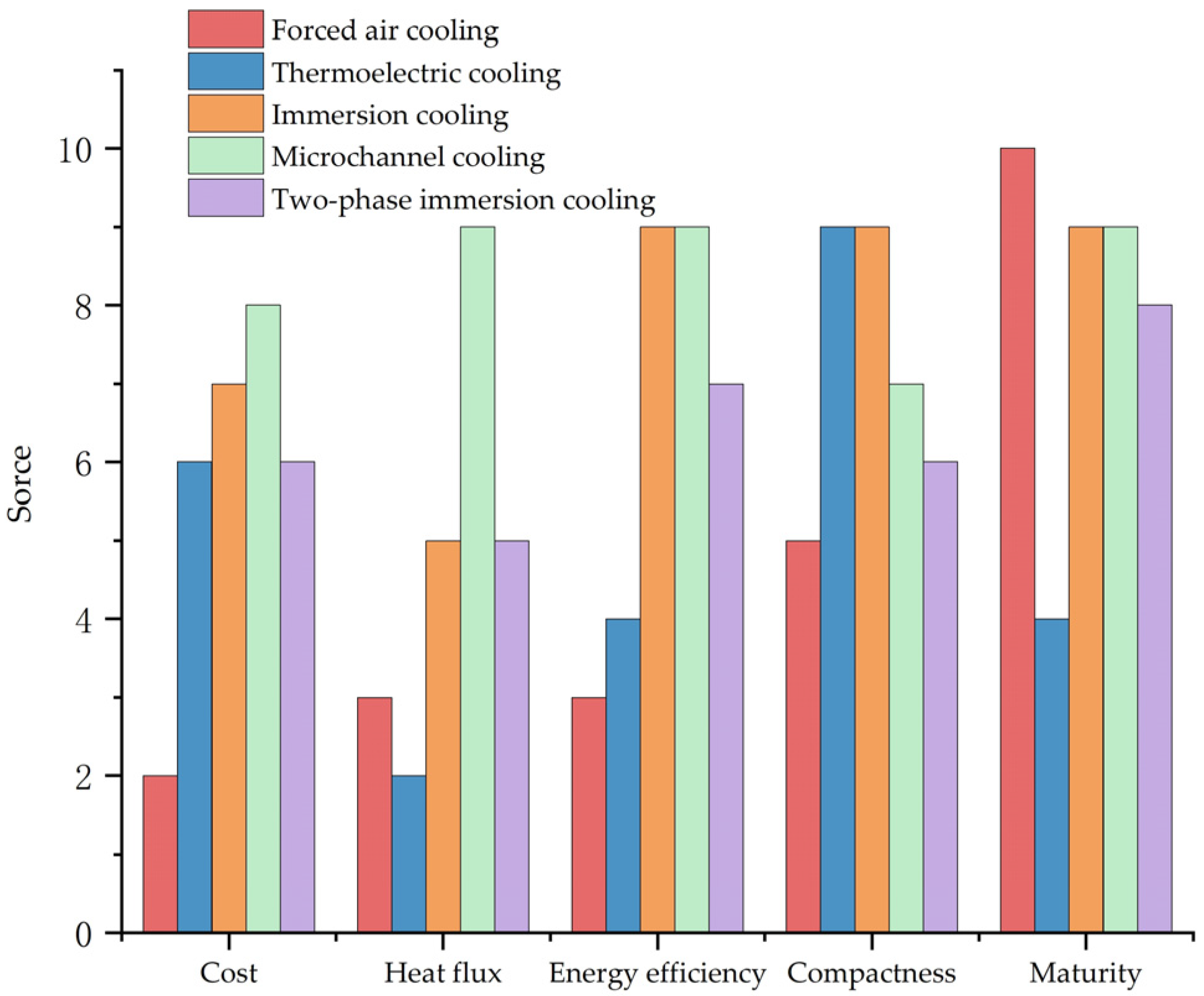
Thermal management for pulsed power supplies is recognized as a quintessential multi-level problem, spanning the entire three-tier hierarchy of component, board, and system scales. Figure 10 illustrates the typical heat dissipation characteristics of the four cooling architectures. Consequently, the selection of the cooling architecture necessitates a comprehensive trade-off analysis across several key metrics, including peak heat load, heat flux density, system volume, energy efficiency, compactness, and cost. To facilitate this selection, Table 4 provides a systematic comparison of these methods, summarizing their typical heat transfer coefficients (h), applicable levels, and respective advantages and disadvantages. Among these options, phase-change cooling is particularly well-suited for next-generation high-voltage pulse generators operating at elevated power levels and repetition rates. This suitability stems from its capability to rapidly handle thermal transients and severe high heat flux concerns [153]. In addition to choosing the best cooling technique, using materials that can withstand high temperatures during the manufacturing and packaging of components is a keyway to address thermal issues. This focus on durable materials greatly reduces the risk of heat-related damage and naturally boosts the reliability of the pulsed power supply.

3.2. Multi-Module Synchronous Triggering

To increase voltage and current output, pulse power systems commonly connect multi-stage Marx, LTD, and PFN modules in series and parallel, boosting their output capabilities. Ideally, each module’s rise time should be perfectly synchronized so their output matches in phase and amplitude at the load. The ideal output is expressed as (6).
V t o t a l ( t ) = i = 1 N V i ( t )
when accounting for jitter ( δ i ), the output is represented by (7)
V t o t a l ( t ) = i = 1 N V i ( t δ i )
where Vtotal represents the total output voltage, Vi(t) denotes the output voltage of a single module, and t is the time variable.
Therefore, a larger jitter degrades the rising edge of the output waveform and attenuates the output peak voltage. Asynchronous switching results in non-uniform voltage and current sharing among modules. Prematurely triggered switches endure disproportionate electrical and thermal stresses, whereas delayed switches are susceptible to reverse voltage or severe transient overstress [157]. Under high-repetition-rate conditions, this cumulative stress imbalance accelerates device degradation and compromises system longevity. If the distributed switch array’s trigger jitter exceeds 5 ns, it may cause peak reduction and waveform distortion, and exceeding 20 ns results in unacceptable performance, potentially damaging them or creating hazardous hot spots within components [158]. Therefore, the system’s required synchronization accuracy directly affects both its transient responses and long-term reliability. Making synchronization a primary design goal is crucial from both engineering and scientific perspectives.
In multi-module pulsed power systems, synchronization faces severe challenges as the number of modules scales up. Research indicates that electromagnetic coupling and structural variances lead to a non-linear accumulation of timing errors, a phenomenon referred to as “synergistic jitter deterioration.” Reference [159] clearly illustrates this trend: while a single module operates with a manageable jitter of 4.7 ns, parallel operation of two modules causes a significant increase to the 4.79–9.5 ns range due to mutual interference—an escalation of 20–43%. in a three-module configuration, the combined effects of asymmetric discharge channels and coupling exacerbate the system jitter to 6.38–10.98 ns. This more than twofold increase demonstrates that simple parallel triggering strategies are insufficient for large-scale arrays, necessitating advanced isolation and timing control mechanisms. However, achieving superior synchronization often incurs a steep penalty in terms of system complexity and cost. To resolve the conflict between synchronization precision and system complexity, researchers have developed a spectrum of triggering architectures, extending from robust electrical topologies to ultra-precise optical controls. To elucidate the performance boundaries and applicability of these methodologies, Table 5 presents a comprehensive comparative analysis focusing on their jitter characteristics, scalability, and technical trade-offs.
As indicated in Table 5, current research on triggering technology has shifted significantly from gas and corona-stabilized switches toward solid-state architectures, incorporating advanced FPGA timing control to minimize intrinsic jitter. However, at the system level, mitigating inconsistent switching caused by signal jitter and delay requires more than just device optimization; it necessitates robust isolation mechanisms (such as magnetic or optical isolation) and low-inductance isochronous transmission lines. Fundamentally, the core technical challenge arises from an irreconcilable conflict between the demand for extremely high synchronization accuracy and the system’s inherent parasitic effects and EMI.

3.3. Electromagnetic Interference

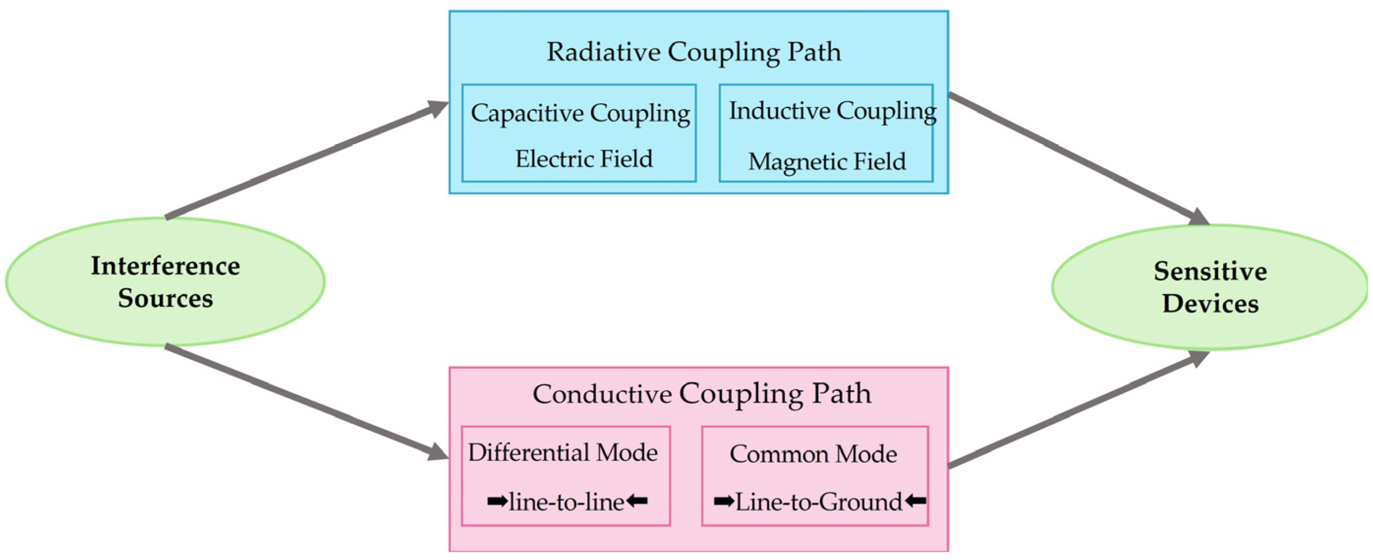
The generation of EMI is fundamentally driven by extreme electrical transients during pulse discharge. Regarding conduction coupling, the interference spectrum is heavily dependent on the switching topology and parasitic elements. Quantitative analysis of a 2.4 kV pulsed power system demonstrates that conducted EMI exhibits distinct characteristics across frequency bands. In the low-frequency domain (typically 20 kHz to 1 MHz), Differential mode (DM) noise dominates, driven by the fundamental switching frequency and its harmonics. the circulation of these high-amplitude DM currents through circuit resistive elements (particularly the ESR of capacitors) significantly exacerbates joule heating Conversely, in the high-frequency domain (> 1 MHz), Common mode (CM) noise becomes prevalent. This transition is fundamentally driven by the parasitic capacitance (Cp) between the switching devices and the heatsink, which provides a low-impedance path for high dV/dt currents. Furthermore, unmitigated stray inductances in the circuit layout often interact with these capacitances to induce significant resonance peaks in the 10–30 MHz range. Crucially, this CM interference activates two distinct failure mechanisms: firstly, the high-frequency voltage stress across the insulation interfaces promotes partial discharge and dielectric breakdown; secondly, the coupling of CM transients into sensitive control loops induces signal corruption. This can precipitate false triggering events, subjecting the power switches to catastrophic shoot-through faults or cumulative electro-thermal overstress [166]. However, this interference generates electromagnetic radiation characterized by an extremely wide spectrum. Via conduction coupling, it affects the internal control circuitry, accelerates the aging of internal switching elements, and interferes with external measurement equipment. This interference notably disrupts the normal operation of oscilloscopes, hindering system analysis by personnel, and also negatively impacts adjacent circuitry [167]. The EMI problem in pulsed power systems fundamentally adheres to the classic source–path–receptor model (interference source–coupling path–sensitive device), as illustrated in Figure 11. Conduction coupling transfers interference directly via physical connections, while radiation coupling propagates as electric and magnetic field energy through free space and surrounding media.
Firstly, at the packaging level, the primary strategy focuses on minimizing parasitic capacitance and inductance through structural innovation. Studies indicate that common-mode (CM) current can be effectively curtailed by replacing conventional direct bonded copper (DBC) ceramics with low-permittivity materials (such as epoxy) and by minimizing the copper area at the DBC’s base. This optimization yields a 52.5% reduction in CM capacitance and a noise attenuation of 4–5 dB during steady-state operation, all while maintaining thermal stability [169]. Furthermore, for high-frequency switching modules, integrating a π-type common-mode filter (CMF) directly within the GaN module helps mitigate the impact of parasitic inductance in the interference path, achieving a significant noise reduction of up to 50 dB across the 10–100 MHz frequency range [170].
Secondly, regarding filtering, the objective is to actively cancel parasitic parameters and suppress broadband noise. One innovative technique involves magnetically coupling two inductors onto a single core to generate negative capacitance. This effectively neutralizes the inductor’s equivalent parallel capacitance (EPC), reducing interference by 10 dB at frequencies above 5 MHz [171]. Moreover, to address wideband noise, a hybrid suppression strategy combining an active common-mode canceler (ACMC) with passive CMFs has been proposed. Experimental results demonstrate that this synergistic approach suppresses total conducted emissions by over 30 dB, ensuring signal levels remain well below standard regulatory limits [172].
Thirdly, material-level optimization aims to enhance EMC through advanced polymer nanocomposites. Unlike traditional metals, emerging composites reinforced with conductive fillers (such as graphene, CNTs, and MXenes) prioritize an absorption-dominated mechanism, effectively reducing secondary electromagnetic pollution. For instance, novel segregated structures facilitate the formation of efficient conductive networks at low filler loadings, attaining electrical conductivities exceeding 40 S/m and a Shielding effectiveness (SE) of 50–70 dB in the X-band (8.2–12.4 GHz) [173]. Similarly, conducting polymers—such as polyaniline, polypyrrole, and polythiophene—exhibit superior EMI shielding capabilities, realizing an SE of 60.2 dB in the 8–12 GHz range. Concurrently, the development of low-k dielectric materials further enhances signal integrity by minimizing capacitive coupling [174].
In summation, the EMI problem is characterized by its pervasive and latent nature. Fundamentally, the strategy involves segmenting the primary space into multiple distinct regions and implementing optimized shielding designs to maximally suppress the coupled interference currents, electric fields, and magnetic fields.

3.4. Reliability Characteristics of Typical Topologies

While fundamental failure mechanisms—electrical, thermal, magnetic, and mechanical—are universal, the hierarchy of dominant stresses and mitigation strategies is intrinsically linked to the specific topology of the pulsed power supply (PPS). For instance, a design optimized for a Marx generator may be incompatible with a PFN. Consequently, analyzing reliability from a topological perspective is a prerequisite for effective system design. Table 6 presents a comparative analysis of the reliability characteristics of four representative PPS topologies across four dimensions: dominant stresses, critical vulnerable components, typical failure modes, and targeted design strategies.
Switching element failures are a critical bottleneck for high-voltage impulse generators. For Marx generators, the dominant issue is switch electrode erosion due to material ablation, whereas Blumlein lines are vulnerable to catastrophic overcurrent-induced switch breakdown caused by high current densities. Beyond switching, insulation and passive component degradation are universal challenges for all topologies in Table 6. While Marx generators suffer primarily from capacitor dielectric aging, LTDs, PFNs, and Blumlein lines exhibit similar vulnerabilities, including capacitor or inductor failure and dielectric breakdown in modules and transmission lines. Notably, LTDs encounter unique thermal stresses arising from magnetic core loss; without effective thermal management, this heating significantly accelerates insulation degradation. Regardless of topologies, common critical requirements remain. Rigorous thermal management and EMC design are paramount to minimizing failure risks. Fundamentally, reliability is not an intrinsic, static constant; it is a dynamic characteristic that evolves under the unique stress profiles of each topology.

3.5. Synergistic Impact of System Integration on Reliability

This section reviews common reliability challenges in integrating pulsed power supply systems. Reliability depends on complex interactions between electrical, thermal, and magnetic fields, not just on individual parts. For example, in a solid-state Marx generator, microchannel cooling introducing parasitic parameters and EMI, complicate system design. Achieving low-jitter synchronization also increases EMI and adds complexity to EMC considerations [157]. Moreover, the switch’s junction temperature directly influences its switching characteristics, meaning an unstable thermal field compromises switch synchronization and induces jitter [181]. These intertwined phenomena demonstrate that system-level challenges—including thermal management, EMC, trigger synchronization and topological characteristics—are not isolated, but rather interwoven into a tightly coupled challenge network. Furthermore, the distinct reliability profiles of different PPS topologies arise from how they configure and stress the basic components. The choice of topology dictates the primary stress vectors, which in turn prioritizes different hierarchies of the aforementioned system challenges, making a universal optimization approach unrealistic.
Therefore, achieving high reliability in pulsed power systems necessitates a component-driven, system-aware design philosophy that explicitly accounts for cross-domain interactions. The properties of components define the system-level constraints, but these constraints are entangled. Future design must evolve from independent, layered optimization to a holistic co-design framework, which requires multi-physics modeling and co-simulation tools that can capture the electro-thermal–magnetic coupling both within components and across system integration choices, enabling designers to navigate the inherent trade-offs and preemptively decouple failure pathways for robust, long-term operation.

4. Reliability Issues and Solutions in Extreme Environments

The above review provides a comprehensive analysis of reliability challenges and mitigation strategies for pulsed power supplies at both the component and system integration levels. However, pulsed power supplies seldom function within ideal laboratory conditions; rather, their ultimate reliability depends greatly on specific application scenarios. Variations in performance criteria, operational modes, and external environments cause each scenario to introduce distinct stressors to the power system, resulting in different failure modes and reliability requirements.

4.1. Aerospace

Leveraging its high-power density and adjustable frequency, the pulsed power supply is extensively utilized in the aerospace domain for critical applications such as satellite radar systems and plasma thrusters. However, space presents a comprehensive extreme environment—distinct from terrestrial conditions. Radiation effects, vacuum exposure, potentially leading to internal component failure, mission termination, and irreparable financial loss. In aerospace applications, the vacuum environment precludes convective heat transfer, leading to thermal accumulation and elevated junction temperatures under repetitive pulse operations. Concurrently, low ambient pressure and material outgassing compromise dielectric strength. When exacerbated by the high dV/dt characteristic of power switches, these factors significantly increase the susceptibility to surface flashover [182]. Furthermore, the radiation environment exerts a synergistic effect with the electric field. High-energy particles can trigger Single event burnout (SEB) in power devices, particularly during the off-state. Given that SEB sensitivity exhibits an exponential dependence on operating voltage, the implementation of strict voltage derating is imperative to mitigate these stochastic failure modes [183,184]. Consequently, mitigation strategies prioritize decoupling these environmental-electrical synergies. Insulation degradation is mitigated by employing radiation-hardened materials and robust packaging [185]. Furthermore, the exponential risk of SEB is suppressed through strict voltage derating and the integration of protection circuits [184].

4.2. Navigation

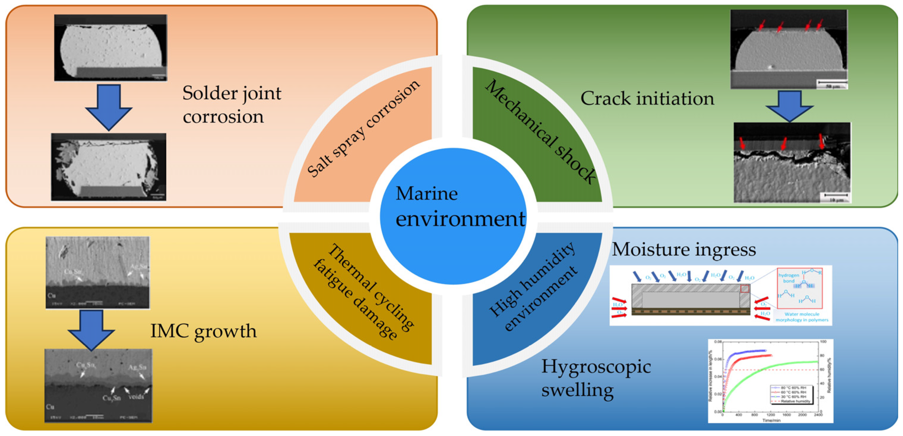
Leveraging its high energy density and rapid response capability, the pulsed power supply exhibits immense potential in maritime applications, including ship integrated power systems, directed energy weapons, and underwater detection. The marine environment creates major reliability challenges due to corrosion from salt and humidity, ongoing temperature changes, and strong mechanical stress from seawater. Figure 12 schematically illustrates the environmental stresses encountered by pulsed power supplies in the marine environment. The presence of salt mist and high humidity facilitates the formation of conductive aqueous films on PCB surfaces. Under continuous electric bias, this environment induces electrochemical migration (ECM), where metal ions dissolve at the anode and migrate toward the cathode to form dendritic structures. This process progressively degrades the surface insulation resistance (SIR), eventually leading to short-circuit failures [186]. Simultaneously, the system is subjected to thermal cycling arising from both environmental fluctuations and pulsed load operations. Due to the mismatch in coefficients of thermal expansion (CTE) among semiconductor chips, solder layers, and substrates, cyclic shear stress is generated at bonding interfaces. This stress induces the accumulation of plastic strain within solder joints, driving crack propagation and resulting in eventual fatigue fracture [187]. Therefore, the mitigation strategy focuses on blocking the electrochemical reaction path and alleviating interfacial stress. To prevent ECM, conformal coatings and hermetic housings are applied to isolate the circuit from moisture and chloride ions, effectively cutting off the electrolyte formation. To mitigate thermal fatigue, the design employs CTE-matched baseplates and advanced silver sintering technologies. These materials reduce the shear strain range experienced by the interconnection layers, thereby extending the fatigue life under cyclic thermal loads [186,188].

4.3. Geological Exploration and Resource Exploration

Leveraging its potent instantaneous electromagnetic field excitation capability, the pulsed power supply has become central to geological exploration equipment, such as those used for deep subsurface surveying and oil resource identification. However, deployment in extreme environments (such as deserts and plateaus) imposes a dual constraint: the system must maintain mobility while ensuring reliable operation.
In desert environments, system reliability is fundamentally challenged by the disruption of thermal equilibrium. The primary stressor is the high ambient temperature induced by prolonged solar radiation, which accelerates the degradation of internal materials and reduces convective heat transfer efficiency, ultimately resulting in an increase in ESR. Furthermore, windblown sand tends to accumulate on heat dissipation surfaces, forming a thermal insulation layer. This accumulation creates a positive feedback loop with the high-temperature environment, significantly increasing the system’s thermal resistance Rth [193]. Consequently, internal heat dissipation is impeded, causing the junction temperature of power devices to rise continuously until system failure occurs. Therefore, mitigation strategies must focus on maintaining thermal balance and implementing sand-resistant designs. The risk of thermal aging is minimized by employing high-temperature tolerant materials such as gold [194], high-temperature tolerant devices and high-efficiency cooling methods. Simultaneously, the ingress of windblown sand is prevented through the use of sealed enclosures or filtration systems.
In high-altitude plateau applications, the reliability of pulsed power supplies is strictly constrained by the coupling of hypobaric and cryogenic conditions. The primary threat is the degradation of air dielectric strength due to the rarefied atmosphere. According to equation 5, Paschen’s Law, the breakdown voltage of the air gap decreases significantly at lower pressures, drastically increasing the risk of corona inception and surface flashover across high-voltage components [195].
V B = B p d ln ( A p d ) ln ( ln ( 1 + 1 γ s e ) )
where VB denotes the gas breakdown voltage, p is the gas pressure, and d represents the inter-electrode distance. A and B denote Townsend’s first and second ionization coefficients, while γse represents the secondary electron emission coefficient. Furthermore, extreme low temperatures cause the electrolyte in energy storage capacitors to freeze. This leads to a sharp rise in ESR and a reduction in capacitance, which distorts the output pulse waveform and degrades energy transfer efficiency [196]. Therefore, mitigation strategies must address both corona discharge hazards and the adverse effects of low temperatures. Key measures include the utilization of corona-resistant materials, increasing inter-electrode spacing, and selecting low-temperature tolerant devices.

4.4. Comparative Analysis and Mitigation Strategies

In conclusion, while specific environmental manifestations vary significantly, the fundamental reliability challenge for pulsed power supplies remains consistent: the coupling of environmental physics with high-voltage electrical stress. Environmental factors serve as catalysts that significantly accelerate the degradation of components under electrical load. External stressors do not act in isolation but exacerbate intrinsic failure mechanisms such as thermal aging and insulation breakdown. Table 7 provides a comprehensive summary of these environmental-physical interactions and corresponding mitigation strategies. This systematic mapping underscores that in future, ensuring the reliability of pulsed power systems in extreme scenarios requires a transition from empirical retrofitting to physics-based predictive design, fundamentally aiming to decouple sensitive components from these degradation pathways.

5. Conclusions and Prospects

Serving as the fundamental technological foundation for transient energy release and ultra-high-power output, the reliability of pulsed power supplies is critical in assessing both system engineering readiness and sustained operational capacity. This paper systematically reviews recent progress at three levels, component technologies, system integration, and adaptability to harsh environments, identifying a distinct “layered optimization” trend in current technologies. At the component level, innovations in dielectric modification, composite films, porous electrodes, and wide-bandgap semiconductors have significantly enhanced energy density, temperature stability, and switching performance. Concurrently, advanced packaging has improved the management of internal electro-thermal stresses under high-repetition pulses. At the system level, solutions for thermal management, multi-module synchronization, and EMI suppression are summarized. At the application level, protective designs tailored for extreme environments are discussed to ensure survivability.
However, a fundamental bottleneck remains in this layered approach. Failures in PPS operation are intrinsically the result of dynamic coupling, transmission, and evolution of multi-physics stresses (electrical–thermal–magnetic–mechanical) across the “Component–System–Environment” hierarchy. Existing research largely addresses static stresses in isolation or considers simple unidirectional impacts, failing to establish a framework that bridges these layers to describe the dynamic synergistic evolution of failures. This lack of systemic methodology means that high reliability at the component level does not necessarily translate into system-level longevity. This has resulted in notable voids within the current body of knowledge regarding PPS reliability, particularly at three key levels:
  • Current research predominantly focuses on failure analysis of individual components or interactions within limited physical fields. There is a notable lack of investigation into the performance interaction and degradation correlation among multiple components under coupled electrical–thermal–magnetic–mechanical stresses. Consequently, a widely accepted system-level prediction model capable of describing the cross-component propagation and evolution of failures has yet to be established.
  • Current reliability verification experiments are predominantly conducted under standardized or idealized conditions. They fail to adequately replicate the dynamic coupling of electrical–thermal–magnetic–mechanical stresses and environmental factors inherent in real-world applications. Consequently, there is a significant discrepancy between laboratory data and actual field performance.
  • Current condition monitoring technologies are primarily focused on reactive fault detection and alarming. There is a distinct lack of comprehensive capabilities for real-time health assessment and prognostic prediction.
In conclusion, this systematic review highlights the critical need to transcend the limitations of traditional layered design. Future research must prioritize bridging gaps in multi-component synergistic modeling, realistic system verification, and intelligent health management. By adopting multi-scale modeling and simulation, designing coupled multi-stress accelerated life testing protocols, and employing hybrid intelligent algorithms combining data-driven and model-driven approaches, a full-lifecycle reliability assurance system can be established. This framework will be pivotal in facilitating the deployment of next-generation high-performance and high-reliability PPS.

Funding

This project was supported by the Tianjin Municipal Education Commission Scientific Research Project (Natural Science, Grant No. 2023KJ301) and the Youth Fund for Scientific Research Projects of Higher Education Institutions in Hebei Province of China (No. QN2025339). The Article Processing Charge (APC) was funded by the Youth Fund for Scientific Research Projects of Higher Education Institutions in Hebei Province of China.

Data Availability Statement

No new data were created or analyzed in this study.

Conflicts of Interest

The authors declare no conflict of interest.

References

  1. Martin, J.C. Nanosecond pulse techniques. Proc. IEEE 1992, 80, 934–945. [Google Scholar] [CrossRef]
  2. Jiang, S.; Hu, H.; Wang, S.; Li, L.; Peng, T. Design of pulsed power supply for repetitive pulsed high magnetic field for water electrolysis. Rev. Sci. Instrum. 2021, 92, 114708. [Google Scholar] [CrossRef] [PubMed]
  3. Dong, J.; Gui, Y.; Li, J.; Zhang, J. Design of Pulsed Power Supply for Electromagnetic Launch. High Volt. Eng. 2007, 33, 105–107. [Google Scholar]
  4. Novac, B.; Istenic, M.; Luo, J.; Smith, I.; Brown, J.; Hubbard, M.; Appelgren, P.; Elfsberg, M.; Hurtig, T.; Möller, C.; et al. A 10-GW pulsed power supply for HPM sources. IEEE Trans. Plasma Sci. 2006, 34, 1814–1821. [Google Scholar] [CrossRef]
  5. Qiu, H.; Wang, S.H.; Sun, F.J.; Wang, Z.G.; Zhang, N.M. Transient Electromagnetic Field Analysis for the Single-Stage Fast Linear Transformer Driver with Two Different Configurations Using the Finite-Element Method and Finite Integration Technique. IEEE Trans. Magn. 2020, 56, 7515805. [Google Scholar] [CrossRef]
  6. Borthakur, S.; Talukdar, N.; Neog, N.K.; Borthakur, T.K.; Kumar, R.; Verma, R.; Shyam, A. 200 kJ Pulsed Power System for Pulsed Plasma Device. IEEE Trans. Plasma Sci. 2017, 45, 1769–1775. [Google Scholar] [CrossRef]
  7. Jang, S.-R.; Ryoo, H.-J.; Ok, S.-B. Pulsed-Power System for Leachate Treatment Applications. J. Power Electron. 2011, 11, 612–619. [Google Scholar] [CrossRef]
  8. Tseng, S.Y.; Wu, T.F.; Wu, M.W. Bipolar narrow-pulse generator with energy-recovery feature for liquid-food sterilization. IEEE Trans. Ind. Electron. 2008, 55, 123–132. [Google Scholar] [CrossRef]
  9. Katiyo, W.; Yang, R.; Zhao, W. Effects of combined pulsed electric fields and mild temperature pasteurization on microbial inactivation and physicochemical properties of cloudy red apple juice (Malus pumila Niedzwetzkyana (Dieck)). J. Food Saf. 2017, 37, e12369. [Google Scholar] [CrossRef]
  10. Ferraz, L.; Silva, E. Pulsed electric field-assisted extraction techniques for obtaining vegetable oils and essential oils: Recent progress and opportunities for the food industry. Sep. Purif. Technol. 2025, 354, 128833. [Google Scholar] [CrossRef]
  11. Golberg, A.; Yarmush, M. Nonthermal Irreversible Electroporation: Fundamentals, Applications, and Challenges. IEEE Trans. Biomed. Eng. 2013, 60, 707–714. [Google Scholar] [CrossRef] [PubMed]
  12. Jiang, C.; Davalos, R.; Bischof, J. A Review of Basic to Clinical Studies of Irreversible Electroporation Therapy. IEEE Trans. Biomed. Eng. 2015, 62, 4–20. [Google Scholar] [CrossRef] [PubMed]
  13. Jiang, H.; Jiang, X.; Wang, Z.; Sun, F.; Wei, H.; Lou, C.; Qiu, A. Discharge characteristics of trigger brick gas switches for 12-stage linear transformer driver. High Power Laser Part. Beams 2024, 36, 115001. [Google Scholar]
  14. Lv, Y.; Wang, H.; Liu, X.; Lu, S.; Lian, H. A High Frequency Bipolar Nanosecond Pulse Generator with High Voltage Gain Based on Inductive Discharge for DBD Application. IEEE Trans. Power Electron. 2025, 40, 17998–18010. [Google Scholar] [CrossRef]
  15. Pandit, P.P.; Jency, J.G.; Babu, M.; Kumar, K.; Nirmal, D. Fabrication of ultra flexible super capacitor using polyvinylidene fluoride. In Proceedings of the 2017 International Conference on Innovations in Electrical, Electronics, Instrumentation and Media Technology (ICEEIMT), Coimbatore, India, 3–4 February 2017. [Google Scholar]
  16. Liu, W.; Sun, X.; Yan, X.; Gao, Y.; Zhang, X.; Wang, K.; Ma, Y. Review of Energy Storage Capacitor Technology. Batteries 2024, 10, 271. [Google Scholar] [CrossRef]
  17. He, Y.; Wang, F.; Du, G.; Pan, L.; Wang, K.; Gerhard, R.; Plath, R.; Rozga, P.; Trnka, P. Revisiting the thermal ageing on the metallised polypropylene film capacitor: From device to dielectric film. High Volt. 2023, 8, 305–314. [Google Scholar] [CrossRef]
  18. Luo, C.; Cong, P.; Zhang, T.; Zhong, X.; Luo, W. Prediction and experimental verification of erosion resistance of gas switch electrode materials. AIP Adv. 2021, 11, 055206. [Google Scholar] [CrossRef]
  19. Sun, H.; Liu, W.; Liu, K. Summary of research on control technology of pulsed power supply in electromagnetic launch system. In Proceedings of the 16th Annual Conference of China Electrotechnical Society: Volume II, Beijing, China, 24–26 September 2021. [Google Scholar]
  20. Bluhm, H. Pulsed Power Systems: Principles and Applications, 1st ed.; Springer: Berlin/Heidelberg, Germany, 2006; pp. 7–54. [Google Scholar]
  21. Aghmadi, A.; Mohammed, O. Energy Storage Systems: Technologies and High-Power Applications. Batteries 2024, 10, 141. [Google Scholar] [CrossRef]
  22. Chen, Z.; Sun, J.; Dong, Z.; Ren, J.; Jia, W.; Guo, F.; Xie, L.; Wu, W.; Yao, X. Failure behavior of dielectric films for peaking capacitor subjected to surface flashover under nanosecond pulses. AIP Adv. 2023, 13, 125203. [Google Scholar] [CrossRef]
  23. Xu, Y.; Xiang, Y.; Wan, Q.; Yang, R.; Xiao, H.; Ding, H.; Li, L. A Dual-Capacitors Type Energy Recovery Power System for Repetitive Pulsed High Magnetic Fields. J. Low Temp. Phys. 2013, 170, 488–495. [Google Scholar] [CrossRef]
  24. Wang, J.; Gao, D.-Q.; Shen, W.-Z.; Yan, H.-B.; Mao, L.-J. Reliability of DC-link capacitor in pulsed power supply for accelerator magnet. Nucl. Sci. Tech. 2024, 35, 151. [Google Scholar] [CrossRef]
  25. Kolobov, V.; Barannik, M.; Selivanov, V.; Kuklin, D. A current source with an inductive energy storage for measuring pulse impedances of grounding connections. Instrum. Exp. Tech. 2014, 57, 572–578. [Google Scholar] [CrossRef]
  26. Liebfried, O. Review of Inductive Pulsed Power Generators for Railguns. IEEE Trans. Plasma Sci. 2017, 45, 1108–1114. [Google Scholar] [CrossRef]
  27. Perez, J.; Sugai, T.; Jiang, W.; Tokuchi, A.; Horie, M.; Ohshio, Y.; Ueno, K. High current pulse forming network switched by static induction thyristor. Matter Radiat. Extremes 2018, 3, 261–266. [Google Scholar] [CrossRef]
  28. Vazquez, S.; Lukic, S.M.; Galvan, E.; Franquelo, L.G.; Carrasco, J.M. Energy Storage Systems for Transport and Grid Applications. IEEE Trans. Ind. Electron. 2010, 57, 3881–3895. [Google Scholar] [CrossRef]
  29. Kondoh, J.; Funamoto, T.; Nakanishi, T.; Arai, R. Energy characteristics of a fixed-speed flywheel energy storage system with direct grid-connection. Energy 2018, 165, 701–708. [Google Scholar] [CrossRef]
  30. Mousavi, G.S.M.; Faraji, F.; Majazi, A.; Al-Haddad, K. A comprehensive review of Flywheel Energy Storage System technology. Renew. Sustain. Energy Rev. 2017, 67, 477–490. [Google Scholar] [CrossRef]
  31. Huang, Y.; Wang, L.; Zhang, D.; Chen, L.; Yuan, J.; Xie, W.; Deng, M.; Kong, Y. Electrical and thermal aging analysis of all-film pulsed capacitor. High Power Laser Part. Beams 2024, 36, 025020. [Google Scholar]
  32. Wang, H.; Blaabjerg, F. Reliability of Capacitors for DC-Link Applications in Power Electronic Converters-An Overview. IEEE Trans. Ind. Appl. 2014, 50, 3569–3578. [Google Scholar] [CrossRef]
  33. Chun, J.; Heo, J.; Lee, K.; Ye, B.U.; Kang, B.S.; Yoon, S.-H. Thermal activation energy on electrical degradation process in BaTiO3 based multilayer ceramic capacitors for lifetime reliability. Sci. Rep. 2024, 14, 616. [Google Scholar] [CrossRef]
  34. Ye, X.; Hu, Y.; Zheng, B.; Chen, C.; Feng, R.; Liu, S.; Zhai, G. Reliability assessment of film capacitors oriented by dependent and nonlinear degradation considering three-source uncertainties. Microelectron. Reliab. 2021, 126, 114277. [Google Scholar] [CrossRef]
  35. Liu, H.; Qiu, J.; Zhang, W.; Zhang, M.; Dou, Z.; Chen, L. Lifetime prediction and reliability analysis for aluminum electrolytic capacitors in EV charging module based on mission profiles. Front. Electron. 2023, 4, 1226006. [Google Scholar] [CrossRef]
  36. Umran, H.; Wang, F.; He, Y. Ageing: Causes and Effects on the Reliability of Polypropylene Film Used for HVDC Capacitor. IEEE Access 2020, 8, 40413–40430. [Google Scholar] [CrossRef]
  37. Tortai, J.; Bonifaci, N.; Denat, A.; Trassy, C. Diagnostic of the self-healing of metallized polypropylene film by modeling of the broadening emission lines of aluminum emitted by plasma discharge. J. Appl. Phys. 2005, 97, 053304. [Google Scholar] [CrossRef]
  38. Gupta, A.; Yadav, O.; DeVoto, D.; Major, J. A review of degradation behavior and modeling of capacitors. In Proceedings of the ASME International Technical Conference and Exhibition on Packaging and Integration of Electronic and Photonic Microsystems, San Francisco, CA, USA, 27–30 August 2019. [Google Scholar]
  39. Choi, J.S.; Kim, D.C.; Shin, H.S.; Yeo, D.H.; Lee, J.H. Effect of oxygen vacancies on dielectric property and reliability of anti-ferroelectric PLZT applicable to EV-MLCC. Bull. Mater. Sci. 2024, 47, 39. [Google Scholar] [CrossRef]
  40. Laadjal, K.; Cardoso, A.J.M. Multilayer Ceramic Capacitors: An Overview of Failure Mechanisms, Perspectives, and Challenges. Electronics 2023, 12, 1297. [Google Scholar] [CrossRef]
  41. Zheng, B.; Ma, R.; Yuan, S. Transient failure mode of (Ba,Ca)(Ti,Zr)O3 pulsed power capacitor based on electromechanical coupling mechanism. Ceram. Int. 2019, 45, 7654–7660. [Google Scholar] [CrossRef]
  42. David, J.; Ciufo, P.; Elphick, S.; Robinson, D. Preliminary Evaluation of the Impact of Sustained Overvoltage on Low Voltage Electronics-Based Equipment. Energies 2022, 15, 1536. [Google Scholar] [CrossRef]
  43. Tu, C.; Chai, M.; Yu, Y.; Guo, Q.; Chen, J.; Xiao, B.; Long, L. Method for monitoring ESR and capacitance based on discharge rule of aluminum electrolytic capacitors. Electr. Power Autom. Equip. 2020, 40, 108–113. [Google Scholar]
  44. Cao, L.; Xi, R.; Zhou, C.; He, G.; Yang, F.; Xu, L.; Li, H. Polymer Capacitor Films with Nanoscale Coatings for Dielectric Energy Storage: A Review. Coatings 2024, 14, 1193. [Google Scholar] [CrossRef]
  45. Tan, D.Q.; Wu, X. A case study of high-temperature polyetherimide film capacitor fabrication. Mater. Today Energy 2022, 30, 101167. [Google Scholar] [CrossRef]
  46. Cheng, R.; Wang, Y.; Men, R.; Lei, Z.; Song, J.; Li, Y.; Guo, M. High-energy-density polymer dielectrics via compositional and structural tailoring for electrical energy storage. Iscience 2022, 25, 104837. [Google Scholar] [CrossRef] [PubMed]
  47. Jian, G.; Jiao, Y.; Feng, L.; Meng, Q.; Yang, N.; Zhu, S.; Lu, M.; Wong, C.-P. High energy density of BaTiO3@ TiO2 nanosheet/polymer composites via ping-pong-like electron area scattering and interface engineering. NPG Asia Mater. 2022, 14, 4. [Google Scholar] [CrossRef]
  48. Zhang, W.; Cheng, X.; Zhen, Y.; Cao, X.; Fu, Z.; Zhang, H.; Wang, X. Enhanced electrical reliability of Zr-doped BaTiO3 nanoceramics: First-principle calculations and experimental studies. J. Am. Ceram. Soc. 2025, 108, e20273. [Google Scholar] [CrossRef]
  49. Wang, J.; Shen, Z.; Liu, R.; Shen, Y.; Chen, L.; Liu, H.; Nan, C. Texture Engineering Modulating Electromechanical Breakdown in Multilayer Ceramic Capacitors. Adv. Sci. 2023, 10, 2300320. [Google Scholar] [CrossRef]
  50. Bahaa, A.; Alhammadi, A.; Lethesh, K.; Susantyoko, R.; Bamgbopa, M. Ionic liquid electrolyte selection for high voltage supercapacitors in high-temperature applications. Front. Chem. 2024, 12, 1349864. [Google Scholar] [CrossRef]
  51. Castillo, J.; Santiago, A.; Judez, X.; Garbayo, I.; Clemente, J.; Morant-Miñana, M.; Villaverde, A.; González-Marcos, J.; Zhang, H.; Armand, M.; et al. Safe, Flexible, and High-Performing Gel-Polymer Electrolyte for Rechargeable Lithium Metal Batteries. Chem. Mater. 2021, 33, 8812–8821. [Google Scholar] [CrossRef]
  52. Feng, M.; Feng, Y.; Zhang, T.; Li, J.; Chen, Q.; Chi, Q.; Lei, Q. Recent Advances in Multilayer-Structure Dielectrics for Energy Storage Application. Adv. Sci 2021, 8, 2102221. [Google Scholar] [CrossRef]
  53. MacDougall, F.; Ennis, J.; Yang, X.; Cooper, R.; Gilbert, J.; Bates, J.; Naruo, C.; Schneider, M.; Keller, N.; Joshi, S.; et al. High energy density capacitors for pulsed power applications. In Proceedings of the 2009 IEEE Pulsed Power Conference, Washington, DC, USA, 28 June–2 July 2009. [Google Scholar]
  54. Hunstig, M.; Schaermann, W.; Broekelmann, M.; Holtkaemper, S.; Siepe, D.; Hesse, H.J. Smart Ultrasonic Welding in Power Electronics Packaging. In Proceedings of the 11th International Conference on Integrated Power Electronics Systems, Berlin, Germany, 24–26 March 2020. [Google Scholar]
  55. Xia, J.; Cao, F.; Chen, X.; Lin, Z.; Song, Y.; Chen, Y.; Yan, S.; Wang, G. Investigation on Discharge Behavior of Antiferroelectric Multilayer Ceramic Capacitors. IEEE Trans. Dielectr. Electr. Insul. 2023, 30, 643–648. [Google Scholar] [CrossRef]
  56. Peng, Z.; Shi, Q.; Zhang, F.; Liu, J.; Nie, X.; Wang, J.; Xu, S.; Wu, D.; Yang, Z.; Chao, X. A new family of high temperature stability and ultra-fast charge-discharge KNN-based lead-free ceramics. J. Mater. Sci. 2022, 57, 9992–10002. [Google Scholar] [CrossRef]
  57. Li, Z.; Li, H.; Qiu, T.; Lin, F.; Wang, Y. Reliability criterion of film capacitor based on moisture diffusion in encapsulation. High Volt. 2023, 8, 1242–1252. [Google Scholar] [CrossRef]
  58. Li, H.; Huang, X.; Li, Z.; Li, H.; Wang, W.; Wang, B.; Zhang, Q.; Lin, F. Modeling of ESR in metallized film capacitors and its implication on pulse handling capability. Microelectron. Reliab. 2015, 55, 1046–1053. [Google Scholar] [CrossRef]
  59. Lv, C.; Liu, J.; Zhang, Y.; Yin, J.; Zhang, X. A High-Resolution Analytical Thermal Modeling Method of Capacitor Bank Considering Thermal Coupling and Different Cooling Modes. IEEE Trans. Power Electron. 2023, 38, 7674–7684. [Google Scholar] [CrossRef]
  60. Rezaei, M.A.; Fathollahi, A.; Akbari, E.; Saki, M.; Khorgami, E.; Teimouri, A.R.; Chronopoulos, A.T.; Mosavi, A. Reliability Calculation Improvement of Electrolytic Capacitor Banks Used in Energy Storage Applications Based on Internal Capacitor Faults and Degradation. IEEE Access 2024, 12, 13146–13164. [Google Scholar] [CrossRef]
  61. Zhang, W.; Li, Y.; Xiao, W.; Zhang, S.; Xiao, X. Identification of electrical breakdown faults in shunt capacitor bank elements using instantaneous negative sequence current. Int. J. Electr. Power Energy Syst. 2025, 170, 110962. [Google Scholar] [CrossRef]
  62. Mansourizadeh, H.; Hosseinpour, M.; Seifi, A.; Shahparasti, M. A 13-level switched-capacitor-based multilevel inverter with reduced components and inrush current limitation. Sci. Rep. 2025, 15, 290. [Google Scholar] [CrossRef]
  63. Khan, M.; Barzegarkhoo, R.; Siwakoti, Y.; Khan, S.; Li, L.; Blaabjerg, F. A new switched-capacitor multilevel inverter with soft start and quasi resonant charging capabilities. Int. J. Electr. Power Energy Syst. 2022, 135, 107412. [Google Scholar] [CrossRef]
  64. Ou, S.; Hassanifar, M.; Votava, M.; Sangwongwanich, A.; Sahoo, S.; Langwasser, M.; Liserre, M.; Blaabjerg, F. Monolithic Data-Driven Condition Monitoring Strategy for MMC Considering C and ESR. IEEE Trans. Power Electron. 2025, 40, 11339–11354. [Google Scholar] [CrossRef]
  65. Zhao, J.; Zhou, Y.; Zhu, Q.; Song, Y.; Liu, Y.; Luo, H. A remaining useful life prediction method of aluminum electrolytic capacitor based on wiener process and similarity measurement. Microelectron. Reliab. 2023, 142, 114928. [Google Scholar] [CrossRef]
  66. Zhao, X.; Wu, H.; Yang, D.; Wei, J.; Li, Z.; Guo, Z.; Zhang, S. Residual Magnetism Elimination Method for Large Power Transformers Based on Energy Storage Oscillation. IEEE Trans. Power Delivery 2025, 40, 2759–2768. [Google Scholar] [CrossRef]
  67. Smirnov, A.; Ivanov, E.; Pronikov, A.; Kutsaev, S. High-Voltage Pulsed Power Generator for Beam Injection Systems. Electronics 2025, 14, 535. [Google Scholar] [CrossRef]
  68. Spielman, R.B.; Froula, D.H.; Brent, G.; Campbell, E.M.; Reisman, D.B.; Savage, M.E.; Shoup, M.J., III; Stygar, W.A.; Wisher, M.L. Conceptual design of a 15-TW pulsed-power accelerator for high-energy-density-physics experiments. Matter Radiat. Extrem. 2017, 2, 204–223. [Google Scholar] [CrossRef]
  69. Kumar, A.; Jeyan, J.V.M.L.; Agarwal, A. Numerical analysis on 10 MJ solenoidal high temperature superconducting magnetic energy storage system to evaluate magnetic flux and Lorentz force distribution. Phys. C-Supercond. 2019, 558, 17–24. [Google Scholar] [CrossRef]
  70. Zhao, X.; Wu, G.; Yang, D.; Xu, G.; Xing, Y.; Yao, C.; Abu-Siada, A. Enhanced detection of power transformer winding faults through 3D FRA signatures and image processing techniques. Electr. Power Syst. Res. 2025, 242, 111433. [Google Scholar] [CrossRef]
  71. Yuan, Q.; Deng, Z.; Ding, W.; Wang, Y.; Wu, J. New advances in solid-state pulse generator based on magnetic switches. Rev. Sci. Instrum. 2022, 93, 051501. [Google Scholar] [CrossRef]
  72. Go, T.; Kanesawa, K.; Yamazaki, N.; Mukaigawa, S.; Takaki, K.; Fujiwara, T. Energy efficiency of inductive energy storage system pulsed power generator using fast recovery diode. IEEJ Trans. Fundam. Mater. 2009, 129, 23–29. [Google Scholar] [CrossRef]
  73. Xu, K.; Guo, Y.; Lei, G.; Zhu, J. A Review of Flywheel Energy Storage System Technologies. Energies 2023, 16, 6462. [Google Scholar] [CrossRef]
  74. Tao, X.; Liu, K. Pulse shaping method for compulsator. High Power Laser Part. Beams 2018, 30, 72–76. [Google Scholar]
  75. Wang, H.; Liu, K.; Zhu, B.; Feng, J.; Ao, P.; Zhang, Z. Analytical Investigation and Scaled Prototype Tests of a Novel Permanent Magnet Compulsator. IEEE Trans. Magn. 2015, 51, 8203309. [Google Scholar] [CrossRef]
  76. Sun, Z.; Liu, Y.; Hao, X. Present status and development trend of pulsed power supplies for railguns. Adv. Technol. Electr. Eng. Energy 2022, 41, 49–63. [Google Scholar]
  77. Hu, D.; Dai, X.; Xie, B.; Li, W.; Yu, H.; Chen, H. Fatigue Life of Flywheel Energy Storage Rotors Composed of 30Cr2Ni4MoV Steel. Energies 2024, 17, 3730. [Google Scholar] [CrossRef]
  78. Manivasagam, R.; Richard, S. Review on recent developments in pulsed high power systems. In Proceedings of the 3rd International Conference on Engineering Facilities Maintenance and Management Technologies (EFM2T’21), Palapye, Botswana, 28–29 October 2021. [Google Scholar]
  79. Sun, L.; Zhang, Y.; Zu, Y.; Guo, J.; Yin, H.; Song, Q.; Tang, X. A solid-state pulse power sub-nanosecond SiC DSRD-based generator with high-voltage and high repetition frequency for pulse discharge water treatment. Environ. Res. 2024, 252, 119053. [Google Scholar] [CrossRef] [PubMed]
  80. Panda, S.K.; Mitra, S.; Mondal, J.; Roy, A. Comparative Study of Different High Voltage Switches Used in Pulsed High Voltage Application. Power Res. J. CPRI 2024, 19, 109–115. [Google Scholar] [CrossRef]
  81. Yao, X.; Zeng, Z.; Chen, J. Electrode erosion of a high energy impulse spark gap switch. Plasma Sci. Technol. 2005, 7, 3157–3160. [Google Scholar] [CrossRef]
  82. Man, L.; Liang, Y.; Zhang, N.; Cao, N.; Wang, Y.; Xue, P. Research on Self-breakdown Performance of Gas Spark Gap Switch. High Volt. Eng. 2021, 57, 146–151. [Google Scholar]
  83. Li, X.; Pei, Z.; Zhang, Y.; Liu, X.; Li, Y.; Zhang, Q. Electrode erosion properties of gas spark switches for fast linear transformer drivers. Phys. Plasmas 2017, 24, 122108–1–122108-13. [Google Scholar] [CrossRef]
  84. Rukin, S.N. Pulsed power technology based on semiconductor opening switches: A review. Rev. Sci. Instrum. 2020, 91, 011501. [Google Scholar] [CrossRef]
  85. Meyers, V.; Voss, L.; Flicker, J.D.; Rodriguez, L.G.; Hjalmarson, H.P.; Lehr, J.; Gonzalez, N.; Pickrell, G.; Ghandiparsi, S.; Kaplar, R. Photoconductive Semiconductor Switches: Materials, Physics, and Applications. Appl. Sci. 2025, 15, 645. [Google Scholar] [CrossRef]
  86. Wang, J.; Chung, H.S.-H.; Li, R.T.-H. Characterization and Experimental Assessment of the Effects of Parasitic Elements on the MOSFET Switching Performance. IEEE Trans. Power Electron. 2013, 28, 573–590. [Google Scholar] [CrossRef]
  87. Wu, H.; He, Z.; Guo, R.; Ma, J.; Zhao, H.; Chen, X.; Chen, W.; Xu, T. Characterization of the high current triggered vacuum switch. Vacuum 2012, 86, 1911–1915. [Google Scholar] [CrossRef]
  88. Scholfield, D.W.; Butcher, M.D.; Hilko, B.; Dorr, G. Vacuum switch performance in a 1.2 MJ pulse forming network. Rev. Sci. Instrum. 2008, 79, 024703. [Google Scholar] [CrossRef] [PubMed]
  89. Xie, C.; Tan, X.; Du, T.; Tang, B.; Shang, S.; Li, R.; Li, Z. Electrode erosion research of gas spark gap. High Power Laser Part. Beams 2014, 26, 131–139. [Google Scholar]
  90. Zhong, W.; Liu, Y.; Xu, A.; Shang, S.; Jin, D. Experimental investigation of electrode erosion of triggered spark gap. In Proceedings of the 27th International Symposium on Discharges and Electrical Insulation in Vacuum (ISDEIV), Suzhou, China, 18–23 September 2016. [Google Scholar]
  91. Sun, Q.; Zhou, Q.; Yang, W.; Dong, Y.; Zhang, H.; Song, M.; Zhou, M.; Yang, W. Modeling of Electrode Erosion Process in Gas Spark Switch. Plasma Chem. Plasma Process. 2023, 43, 1195–1215. [Google Scholar] [CrossRef]
  92. Wu, J.; Han, R.; Ding, W.; Qiu, A.; Tang, J. Note: Erosion of W-Ni-Fe and W-Cu alloy electrodes in repetitive spark gaps. Rev. Sci. Instrum. 2018, 89, 026103. [Google Scholar] [CrossRef]
  93. Silakhori, K.; Neghabi, M.; Torabi, R. Investigation on electrode erosion effects in high frequency rotary spark gap switches. Optik 2021, 237, 166763. [Google Scholar] [CrossRef]
  94. Song, F.; Li, F.; Zhang, B.; Zhu, M.; Li, C.; Wang, G.; Gong, H.; Gan, Y.; Jin, X.; Novac, B.M.; et al. Electrode Erosion and Lifetime Performance of a Compact and Repetitively Triggered Field Distortion Spark Gap Switch. IEEE Trans. Plasma Sci. 2020, 48, 212–218. [Google Scholar] [CrossRef]
  95. Li, L.; Li, H.; Li, C.; Qi, X.; Lin, F. Analysis on Electrode Replacement of Spark-Gap Switches with Graphite Electrodes. IEEE Trans. Plasma Sci. 2011, 39, 1874–1880. [Google Scholar] [CrossRef]
  96. Zhang, B.; Gan, Y.; Li, C.; Li, F.; Jin, X.; Song, F. Research on channel resistance and thermal effect characteristics of gas-filled spark gap switch. High Power Laser Part. Beams 2024, 36, 134–139. [Google Scholar]
  97. Zhong, W.; Liu, Y.; Wang, L.; Jin, D.; Tan, X. Statistical analysis of particulate concentration from electrode erosion of gas discharge. J. Phys. D Appl. Phys. 2017, 50, 015202. [Google Scholar] [CrossRef]
  98. Akbar, G.; Di Fatta, A.; Rizzo, G.; Ala, G.; Romano, P.; Imburgia, A. Comprehensive Review of Wide-Bandgap (WBG) Devices: SiC MOSFET and Its Failure Modes Affecting Reliability. Physchem 2025, 5, 10. [Google Scholar] [CrossRef]
  99. Ma, C.-T.; Gu, Z.-H. Review on Driving Circuits for Wide-Bandgap Semiconductor Switching Devices for Mid- to High-Power Applications. Micromachines 2021, 12, 65. [Google Scholar] [CrossRef]
  100. Mao, H.; Wu, B.; Lan, X.; Xia, Y.; Chen, J.; Tang, L. Research on Improving the Avalanche Current Limit of Parallel SiC MOSFETs. Electronics 2025, 14, 2502. [Google Scholar] [CrossRef]
  101. Grome, C.A.; Ji, W. A Brief Review of Single-Event Burnout Failure Mechanisms and Design Tolerances of Silicon Carbide Power MOSFETs. Electronics 2024, 13, 1414. [Google Scholar] [CrossRef]
  102. Wu, R.; Blaabjerg, F.; Wang, H.; Liserre, M.; Iannuzzo, F. Catastrophic Failure and Fault-Tolerant Design of IGBT Power Electronic Converters—An Overview. In Proceedings of the 39th Annual Conference of the IEEE Industrial-Electronics-Society (IECON), Vienna, Austria, 10–14 November 2013. [Google Scholar]
  103. Oliveira, J.; Reynes, J.-M.; Morel, H.; Frey, P.; Perrotin, O.; Allirand, L.; Azzopardi, S.; Piton, M.; Coccetti, F. Test Methodology for Short-Circuit Assessment and Safe Operation Identification for Power SiC MOSFETs. Energies 2024, 17, 5476. [Google Scholar] [CrossRef]
  104. Abbaszada, M.A.; Gajanur, N.; Mazumder, S.K. Assessing the reliability of SiC MOSFET through inverter-like accelerated test vs. power cycling test. Microelectron. Reliab. 2025, 165, 115589. [Google Scholar] [CrossRef]
  105. Duan, G.; Vainshtein, S.N.; Kostamovaara, J.T. Modified High-Power Nanosecond Marx Generator Prevents Destructive Current Filamentation. IEEE Trans. Power Electron. 2017, 32, 7845–7850. [Google Scholar] [CrossRef]
  106. Wang, Y.; Ding, Y.; Yin, Y. Reliability of Wide Band Gap Power Electronic Semiconductor and Packaging: A Review. Energies 2022, 15, 6670. [Google Scholar] [CrossRef]
  107. Huang, T.; Singh, B.P.; Liu, Y.; Norrga, S. Failure Characterization of Discrete SiC MOSFETs under Forward Power Cycling Test. Energies 2024, 17, 2557. [Google Scholar] [CrossRef]
  108. Lelis, A.J.; Green, R.; Habersat, D.B.; El, M. Basic Mechanisms of Threshold-Voltage Instability and Implications for Reliability Testing of SiC MOSFETs. IEEE Trans. Electron. Devices 2015, 62, 316–323. [Google Scholar] [CrossRef]
  109. Volosov, V.; Bevilacqua, S.; Anoldo, L.; Tosto, G.; Fontana, E.; Russo, A.-L.; Fiegna, C.; Sangiorgi, E.; Tallarico, A.N. Positive Bias Temperature Instability in SiC-Based Power MOSFETs. Micromachines 2024, 15, 872. [Google Scholar] [CrossRef]
  110. Weckbrodt, J.; Ginot, N.; Batard, C.; Azzopardi, S. Monitoring of Gate Leakage Current on SiC Power MOSFETs: An Estimation Method for Smart Gate Drivers. IEEE Trans. Power Electron. 2021, 36, 8752–8760. [Google Scholar] [CrossRef]
  111. Ouaida, R.; Berthou, M.; Leon, J.; Perpina, X.; Oge, S.; Brosselard, P.; Joubert, C. Gate Oxide Degradation of SiC MOSFET in Switching Conditions. IEEE Electron. Device Lett. 2014, 35, 1284–1286. [Google Scholar] [CrossRef]
  112. AQG 324; Qualification of Power Modules for Use in Power Electronics Converter Units in Motor Vehicles. ECPE European Center for Power Electronics e.V.: Nuremberg, Germany, 2021.
  113. Janabi, A.; Shillaber, L.; Ying, W.; Mu, W.; Hu, B.; Jiang, Y.; Iosifidis, N.; Ran, L.; Long, T. Substrate Embedded Power Electronics Packaging for Silicon Carbide mosfets. IEEE Trans. Power Electron. 2024, 39, 9614–9628. [Google Scholar] [CrossRef]
  114. Wang, L.; Zhang, T.; Yang, F.; Ma, D.; Zhao, C.; Pei, Y.; Gan, Y. Cu Clip-Bonding Method with Optimized Source Inductance for Current Balancing in Multichip SiC MOSFET Power Module. IEEE Trans. Power Electron. 2022, 37, 7952–7964. [Google Scholar] [CrossRef]
  115. Ma, R.; Wang, R.; Fang, H.; Li, P.; Zhao, L.; Wu, H.; Huang, Z.; Tao, J.; Hu, S. A Novel Deep-Trench Super-Junction SiC MOSFET with Improved Specific On-Resistance. Micromachines 2024, 15, 684. [Google Scholar] [CrossRef] [PubMed]
  116. Ou, Y.; Lan, Z.; Hu, X.; Liu, D. Novel SiC Trench MOSFET with Improved Third-Quadrant Performance and Switching Speed. Micromachines 2024, 15, 254. [Google Scholar] [CrossRef] [PubMed]
  117. Zhang, X.; Zhao, X.; Li, W.; Wang, Z.; Liao, A.; Song, Y.; Wang, Y.; Zhang, L. Ultra-thermostable embedded liquid cooling in SiC 3D packaging power modules of electric vehicles. Energy Convers. Manag. 2023, 276, 116499. [Google Scholar] [CrossRef]
  118. Pavlicek, N.; Mohn, F. Laser bonding of copper ribbons and clips on SiC power MOSFETs with sintered copper bond buffers. In Proceedings of the 8th IEEE Electronics System-Integration Technology Conference (ESTC), Vestfold, Norway, 15–18 September 2020. [Google Scholar]
  119. Lee, I.; Yao, X. Active dv/dt Control with Turn-off Gate Resistance Modulation for Voltage Balancing of Series Connected SiC MOSFETs. In Proceedings of the 2021 IEEE Applied Power Electronics Conference and Exposition (APEC), Phoenix, AZ, USA, 14–17 June 2021. [Google Scholar]
  120. Takayama, H.; Okuda, T.; Hikihara, T. Digital active gate drive of SiC MOSFETs for controlling switching behavior-Preparation toward universal digitization of power switching. Int. J. Circ. Theor. Appl. 2022, 50, 183–196. [Google Scholar] [CrossRef]
  121. Shao, T.; Sun, Y.; Bai, Z.; Zheng, T.Q.; Zhang, Y.; Jia, P. Active Gate Drive Based on Negative Feedback for SiC MOSFETs to Suppress Crosstalk Parasitic Oscillation and Avoid Decreased Efficiency. Electronics 2025, 14, 2100. [Google Scholar] [CrossRef]
  122. Li, Q.; Yang, Y.; Wen, Y.; Zhang, G.; Xing, W. Active Gate Driver with the Independent Suppression of Overshoot and Oscillation for SiC MOSFET Modules. IEEE Trans. Ind. Electron. 2025, 72, 2325–2335. [Google Scholar] [CrossRef]
  123. Xu, C.; Miao, Y. SiC MOSFET Active Gate Drive Circuit Based on Switching Transient Feedback. Energies 2024, 17, 1997. [Google Scholar] [CrossRef]
  124. Huang, Y.; Zhang, J.; Wang, N. A Resonant Auxiliary Drive Circuit for SiC MOSFET to Suppress Crosstalk. Trans. China Electrotech. Soc. 2022, 37, 3004–3015. [Google Scholar]
  125. Yang, C.; Pei, Y.; Wang, L.; Yu, L.; Zhang, F.; Ferreira, B. Overvoltage and Oscillation Suppression Circuit with Switching Losses Optimization and Clamping Energy Feedback for SiC MOSFET. IEEE Trans. Power Electron. 2021, 36, 14207–14219. [Google Scholar] [CrossRef]
  126. Liang, M.; Chen, J.; Jia, P. Analysis of DC-Side Snubbers for SiC Devices Application. Electronics 2022, 11, 3874. [Google Scholar] [CrossRef]
  127. Xue, P.; Hoene, E.; Davari, P. An RC snubber design method to achieve optimized switching noise-loss trade-off of cascode GaN HEMTs. IET Power Electron. 2024, 17, 1583–1593. [Google Scholar] [CrossRef]
  128. Liu, C.; Xu, M.; Chen, S.; Sun, L.; Zhang, L.; Li, Q.; Wang, J. Analysis of carrier dynamics and thermal effect of the GaAs photoconductive semiconductor switch in lock-on mode. J. Phys. D Appl. Phys. 2024, 57, 495101. [Google Scholar] [CrossRef]
  129. Sun, Y.; Hu, L.; Li, Y.; Zhu, L.; Dang, X.; Hao, Q.; Li, X. Research on the thermal failure mechanism of an opposed-contact gallium arsenide photoconductive semiconductor switch in avalanche mode. J. Phys. D Appl. Phys. 2022, 55, 215103. [Google Scholar] [CrossRef]
  130. Xu, J.; Jiang, L.; Cai, P.; Feng, C.; Xiao, H.; Wang, X. Properties Investigation and Damage Analysis of GaN Photoconductive Semiconductor Switch Based on SiC Substrate. Micromachines 2024, 15, 1178. [Google Scholar] [CrossRef]
  131. Chu, X.; Xun, T.; Wang, L.; Liu, J.; Yang, H.; He, J.; Zhang, J. Breakdown Behavior of GaAs PCSS with a Backside-Light-Triggered Coplanar Electrode Structure. Electronics 2021, 10, 357. [Google Scholar] [CrossRef]
  132. Zong, J.; Shi, Y.; Qian, G.; Wang, J.; Wei, Z.; Kong, Y.; Zhang, J.; Chen, T. Performance Enhancement of Planar GaAs Photoconductive Semiconductor Switches by Introducing p-Type Epitaxial Layer. Photonics 2025, 12, 152. [Google Scholar] [CrossRef]
  133. Cai, P.; Jiang, L.; Xu, J.; Xiao, H.; Feng, C.; Wang, Q.; He, T.; Zhou, M.; Wang, X. Design of a lateral photoconductive semiconductor switch with a low resistivity region on semi-insulating GaN to enhance breakdown characteristics. Opt. Commun. 2024, 555, 130332. [Google Scholar] [CrossRef]
  134. Sun, Y.; Hu, L.; Dang, X.; Zhu, L.; Yang, X.; Huang, J.; Li, Y.; Li, X. Investigation on the Mechanism of Triggering Efficiency of High-Power Avalanche GaAs Photoconductive Semiconductor Switch. IEEE Electron. Device Lett. 2021, 42, 1646–1649. [Google Scholar] [CrossRef]
  135. Chen, H.; Wei, J.; Zeng, F.; Jia, C.; Fu, Z.; Li, S.; Qian, B. Influence of the width of triggering region on output characteristics of GaAs photoconductive semiconductor switch. High Power Laser Part. Beams 2023, 35, 154–159. [Google Scholar]
  136. Pokryvailo, A.; Carp, C.; Scapellati, C. High Performance, High-Power Capacitor Charging: Focus on Pulse-to-Pulse Repeatability. In Proceedings of the 25th Annual IEEE Applied Power Electronics Conference and Exposition, Palm Springs, CA, USA, 21–25 February 2010. [Google Scholar]
  137. Oomori, H.; Omura, I. An experimental study on switching waveform design with gate charge control for power MOSFETs. Power Electron. Devices Compon. 2023, 6, 100043. [Google Scholar] [CrossRef]
  138. Tong, X.C. Advanced Materials for Thermal Management of Electronic Packaging, 1st ed.; Springer Science & Business Media: New York, NY, USA, 2011; pp. 1–57. [Google Scholar]
  139. Wang, Y.; Ren, L.; Yang, Z.; Shen, S.; Deng, Z.; Yuan, Q.; Ding, W.; Ding, Z. Heat management technology for solid-state high voltage and high repetitive pulse generators: Towards better effects and reliability. High Volt. 2024, 9, 2–21. [Google Scholar] [CrossRef]
  140. Bergman, T.L. Fundamentals of Heat and Mass Transfer; John Wiley & Sons: Hoboken, NJ, USA, 2011; pp. 5–138. [Google Scholar]
  141. de Bock, H.P.; Chamarthy, P.; Jackson, J.L.; Whalen, B. Investigation and Application of an Advanced Dual Piezoelectric Cooling Jet to a Typical Electronics Cooling Configuration. In Proceedings of the 13th IEEE InterSociety Conference on Thermal and Thermomechanical Phenomena in Electronic Systems (ITherm), San Diego, CA, USA, 30 May–1 June 2012. [Google Scholar]
  142. Sauciuc, I.; Yamamoto, R.; Culic-Viskota, J.; Yoshikawa, T.; Jain, S.; Yajima, M.; Labanok, N.; Amoah-Kusi, C. Carbon Based Thermal Interface Material for High Performance Cooling Applications. In Proceedings of the 14th InterSociety Conference on Thermal and Thermomechanical Phenomena in Electronic Systems (ITherm), Orlando, FL, USA, 27–30 May 2014. [Google Scholar]
  143. Cai, Y.; Wang, Y.; Liu, D.; Zhao, F.-Y. Thermoelectric cooling technology applied in the field of electronic devices: Updated review on the parametric investigations and model developments. Appl. Therm. Eng. 2019, 148, 238–255. [Google Scholar] [CrossRef]
  144. Orville, T.; Tajwar, M.; Bihani, R.; Saha, P.; Hannan, M.A. Enhancing Thermal Efficiency in Power Electronics: A Review of Advanced Materials and Cooling Methods. Thermo 2025, 5, 30. [Google Scholar] [CrossRef]
  145. Back, D.; Drummond, K.P.; Sinanis, M.D.; Weibel, J.A.; Garimella, S.V.; Peroulis, D.; Janes, D.B. Design, Fabrication, and Characterization of a Compact Hierarchical Manifold Microchannel Heat Sink Array for Two-Phase Cooling. IEEE Trans. Compon. Packag. Manuf. Technol. 2019, 9, 1291–1300. [Google Scholar] [CrossRef]
  146. Wang, H.; Xia, X.; Wang, P.; Zhou, B.; Chen, S.; Shi, Y. Study on the pillars structure impacts on the embedded microchannel heat sink. In Proceedings of the 23rd International Conference on Electronic Packaging Technology (ICEPT), Dalian, China, 10–13 August 2022. [Google Scholar]
  147. Sporer, B.J.; Shah, A.P.; Dowhan, G.V.; Shapovalov, R.V.; Packard, D.A.; Wisher, M.; Leckbee, J.J.; Hendricks, K.J.; Hoff, B.W.; Lau, Y.Y.; et al. Multicavity linear transformer driver facility for Z-pinch and high-power microwave research. Phys. Rev. Accel. Beams 2021, 24, 100402. [Google Scholar] [CrossRef]
  148. Zhang, C.; Wang, H.; Huang, Y.; Zhang, L.; Chen, Y. Immersion liquid cooling for electronics: Materials, systems, applications and prospects. Renew. Sustain. Energy Rev. 2025, 208, 114989. [Google Scholar] [CrossRef]
  149. Ristic-Smith, A.; Rogers, D.J. Compact Two-Phase Immersion Cooling with Dielectric Fluid for PCB-Based Power Electronics. IEEE Open J. Power Electron. 2024, 5, 1107–1118. [Google Scholar] [CrossRef]
  150. Tang, G.; Wai, L.C.; Feng, H. Development and Demonstration of a Novel Immersion Two Phase Cooling High Power SiC Power Module. In Proceedings of the IEEE 73rd Electronic Components and Technology Conference (ECTC), Orlando, FL, USA, 30 May–2 June 2023. [Google Scholar]
  151. Ren, L.; Wang, Y.; Yang, Z.; Ding, W. High power and high repetition frequency sub-nanosecond pulse generator with two-phase immersion cooling technique. Rev. Sci. Instrum. 2021, 92, 034716. [Google Scholar] [CrossRef] [PubMed]
  152. Manepalli, V.V.; McAfee, R.C.; Randriambololona, A.M.; Graham, S.; Agonafer, D. Dynamic Thermal Management of a MOSFET Power Module Using a Novel Three-Component Phase Change Material. J. Heat Transf. 2025, 147, 102401. [Google Scholar] [CrossRef]
  153. Aleinikov, E.; Barzdenas, V. Comparative Analysis of High-Voltage High-Frequency Pulse Generation Techniques for Pockels Cells. Appl. Sci. 2025, 15, 10830. [Google Scholar] [CrossRef]
  154. Laloya, E.; Lucía, O.; Sarnago, H.; Burdío, J. Heat Management in Power Converters: From State of the Art to Future Ultrahigh Efficiency Systems. IEEE Trans. Power Electron. 2016, 31, 7896–7908. [Google Scholar] [CrossRef]
  155. Gorecki, K.; Posobkiewicz, K. Cooling Systems of Power Semiconductor Devices-A Review. Energies 2022, 15, 4566. [Google Scholar] [CrossRef]
  156. Dhumal, A.R.; Kulkarni, A.P.; Ambhore, N.H. A comprehensive review on thermal management of electronic devices. J. Eng. Appl. Sci. 2023, 70, 140. [Google Scholar] [CrossRef]
  157. Shi, F.; Chen, P.; Jiang, S.; Zhuang, J.; Rao, J. A Solid-State Marx Generator with Prevention of through Current for Rectangular Pulses. Electronics 2024, 13, 101. [Google Scholar] [CrossRef]
  158. Zhang, H.; Chen, J. Analysis of control signal jitter in the distributed synchronous trigger control system for pulse power combining. J. Phys. Conf. Ser. 2025, 3079, 012022. [Google Scholar] [CrossRef]
  159. Geng, J.; Cheng, X.; Yang, J.; Yang, X.; Chen, R. Research on multi-switch synchronization based on single trigger generator. AIP Adv. 2018, 8, 055117. [Google Scholar] [CrossRef]
  160. Damideh, V.; Btaiche, J.C.; Ho, A.; Spielman, R.B.; Lehr, J.M.; Mehlhorn, T.A.; Hassen, I.; Akoulov, A.; Aranfar, E.; McDonald, A.; et al. Experimental results of a 330 GW impedance-matched Marx generator. Sci. Rep. 2024, 14, 16889. [Google Scholar] [CrossRef]
  161. Chen, L.; Zhu, C.; Zheng, J.; Qiu, J.; Zhao, H.; Liu, K. A Flexible Solid-State Marx Modulator Module Based on Discrete Magnetic Coupling Drivers. Electronics 2023, 12, 3831. [Google Scholar] [CrossRef]
  162. Geng, J.-Y.; Yang, J.-H.; Cheng, X.-B.; Chen, R.; Shu, T. A compact, low jitter, high voltage trigger generator based on fractional-turn ratio saturable pulse transformer and its application. Rev. Sci. Instrum. 2022, 93, 084709. [Google Scholar] [CrossRef] [PubMed]
  163. Wu, M.; Liu, G.; He, M.; Shu, W.; Jiao, Y.; Li, H.; Yao, W.; Liang, X. A Low-Jitter Delay Synchronization System Applied to Ti:sapphire Femtosecond Laser Amplifier. Appl. Sci. 2025, 15, 9424. [Google Scholar] [CrossRef]
  164. Chen, L.; Zou, W.; Zhou, L.; Wang, M.; Liu, Y.; Liu, L.; Deng, M.; Liu, D.; Zhu, J.; Lian, K.; et al. Development of a fusion-oriented pulsed power module. Phys. Rev. Accel. Beams 2019, 22, 030401. [Google Scholar] [CrossRef]
  165. Wang, J.; Wang, Z.; Wei, H.; Shen, Y.; Jiang, H. Fiber-optic controlled high voltage trigger generator for a ten-stage linear transformer driver module. Rev. Sci. Instrum. 2025, 96, 065205. [Google Scholar] [CrossRef]
  166. Nia, M.S.S.; Shamsi, P.; Ferdowsi, M. EMC Modeling and Conducted EMI Analysis for a Pulsed Power Generator System Including an AC-DC-DC Power Supply. IEEE Trans. Plasma Sci. 2020, 48, 4250–4261. [Google Scholar] [CrossRef]
  167. Muttaqi, K.; Haque, M. Electromagnetic interference generated from fast switching power electronic devices. Int. J. Innov. Energy Syst. Power 2008, 3, 19–26. [Google Scholar]
  168. Yuan, L.; Zhang, J.; Liang, Z.; Hu, M.; Chen, G.; Lu, W. EMI challenges in modern power electronic-based converters: Recent advances and mitigation techniques. Front. Electron. 2023, 4, 1274258. [Google Scholar] [CrossRef]
  169. Choi, S.; Choi, J.; Warnakulasooriya, T.; Shin, J.-W.; Imaoka, J.; Yamamoto, M. Improved Packaging of Power Module with Low-Permittivity Material for Low Common-Mode Noise and High Reliability. IEEE Trans. Power Electron. 2024, 39, 14261–14270. [Google Scholar] [CrossRef]
  170. Jia, N.; Tian, X.; Xue, L.; Bai, H.; Tolbert, L.M.; Cui, H. Integrated Common-Mode Filter for GaN Power Module with Improved High-Frequency EMI Performance. IEEE Trans. Power Electron. 2023, 38, 6897–6901. [Google Scholar] [CrossRef]
  171. Li, Y.; Wang, S.; Sheng, H.; Lakshmikanthan, S. Reduction and Cancellation Techniques for the Near Field Capacitive Coupling and Parasitic Capacitance of Inductors. In Proceedings of the EEE Symposium on Electromagnetic Compatibility, Signal Integrity and Power Integrity (EMC, SI & PI), Long Beach, CA, USA, 30 July–3 August 2018. [Google Scholar]
  172. Xue, P.; Davari, P. Comparative Study on Temperature Dependency of dV/dt, dI/dt and EMI Generation for IGBTs, Si and SiC MOSFETs. In Proceedings of the 2025 International Symposium on Electromagnetic Compatibility—EMC Europe, Paris, France, 1–5 September 2025. [Google Scholar]
  173. Bheema, R.K.; Gopu, J.; Bhaskaran, K.; Verma, A.; Chavali, M.; Etika, K.C. A review on recent progress in polymer composites for effective electromagnetic interference shielding properties—structures, process, and sustainability approaches. Nanoscale Adv. 2024, 6, 5773–5802. [Google Scholar] [CrossRef]
  174. Shahapurkar, K.; Gelaw, M.; Tirth, V.; Soudagar, M.E.M.; Shahapurkar, P.; Mujtaba, M.A.; Kiran, M.C.; Ahmed, G.M.S. Comprehensive review on polymer composites as electromagnetic interference shielding materials. Polym. Polym. Compos. 2022, 30, 09673911221102127. [Google Scholar] [CrossRef]
  175. Jiang, W. Review of solid-state linear transformer driver technology. Matter Radiat. Extremes 2018, 3, 159–164. [Google Scholar] [CrossRef]
  176. Ranjan, A.; Abhishek, A.; Kumar, N.; Verma, B.K. Review of Nanosecond Pulse Generator with High-Power Switching Devices. IEEE Trans. Electron. Devices 2024, 71, 5165–5176. [Google Scholar] [CrossRef]
  177. Mazarakis, M.G.; Fowler, W.E.; LeChien, K.L.; Long, F.W.; Matzen, M.K.; McDaniel, D.H.; McKee, R.G.; Olson, C.L.; Porter, J.L.; Rogowski, S.T.; et al. High-Current Linear Transformer Driver Development at Sandia National Laboratories. IEEE Trans. Plasma Sci. 2010, 38, 704–713. [Google Scholar] [CrossRef]
  178. Li, M.J.; Kang, Q.; Tan, J.; Luo, M.; Xiang, F. A High-Power Pulse Generator Based on Pulse Forming Network and Linear Transformer. Laser Part. Beams 2021, 2021, e19. [Google Scholar] [CrossRef]
  179. Shen, Y.; Ye, M.; Liu, Y.; Zhang, H.; Xia, L. Electric Field Enhancement Breakdown Caused by the Pulse Formation and Transmission of Parallel-Plate Blumlein Line. IEEE Trans. Plasma Sci. 2024, 52, 2281–2284. [Google Scholar] [CrossRef]
  180. Zhou, Y.; Liu, B.-Y.; Xie, Y.-Z. Investigation of the waveform quality of a kA-level rectangular pulse generator based on pulse forming network. Rev. Sci. Instrum. 2025, 96, 124709. [Google Scholar] [CrossRef]
  181. Mishra, R.K.; Joshi, D.; Agrawal, P.K. Effect on timing drift due to temperature variation in high voltage pulse power supply. In Proceedings of the 2020 International Conference on Power, Energy, Control and Transmission Systems (ICPECTS), Chennai, India, 10–11 December 2020. [Google Scholar]
  182. He, Y.; Gao, R.; Ma, T.; Zhang, X.; Zhang, X.; Yang, Y. Total Ionizing Dose Effects on Lifetime of NMOSFETs Due to Hot Carrier-Induced Stress. Electronics 2025, 14, 2563. [Google Scholar] [CrossRef]
  183. Pearton, S.J.; Haque, A.; Khachatrian, A.; Ildefonso, A.; Chernyak, L.; Ren, F. Review-Opportunities in Single Event Effects in Radiation-Exposed SiC and GaN Power Electronics. ECS J. Solid State Sci. Technol. 2021, 10, 075004. [Google Scholar] [CrossRef]
  184. Zeng, Q.; Yang, Z.; Wang, X.; Li, S.; Gao, F. Research Progress on Radiation Damage Mechanism of SiC MOSFETs Under Various Irradiation Conditions. IEEE Trans. Electron. Devices 2024, 71, 1718–1727. [Google Scholar] [CrossRef]
  185. Mao, J.; Wang, S.; Shi, Q.; Cheng, Y.; Chen, Y. Excellent Vacuum Pulsed Flashover Characteristics Achieved inDielectric Insulators Functionalized by Electronegative Halogen-Phenyl and Naphthyl Groups. Langmuir 2022, 38, 4129–4137. [Google Scholar] [CrossRef] [PubMed]
  186. Zhao, Q.; Liu, X.; Wang, H.; Zhu, Y.; An, Y.; Yu, D.; Qi, J. Research Progress in Corrosion Protection Technology for Electronic Components. Metals 2023, 13, 1508. [Google Scholar] [CrossRef]
  187. Xu, J.; Guo, Y.; Su, Y.; Tang, R.; Long, X. Growth kinetics of intermetallic compound in solder joints during thermal cycling: A review. In Proceedings of the 23rd Electronics Packaging and Technology Conference, Singapore, 1–3 December 2021. [Google Scholar]
  188. Chen, X.; Zhou, G.; Wang, X.; Xu, H.; Wang, C.; Yao, Q.; Chi, J.; Fu, X.; Wang, Y.; Yin, X.; et al. Progress in semiconductor materials for photocathodic protection: Design strategies and applications in marine corrosion protection. Chemosphere 2023, 323, 138194. [Google Scholar] [CrossRef]
  189. Pongvittayapanu, K.; Srisrual, A.; Fakpan, K. Effect of thermal cycling and vibration on cracking in Sn-3.0 Ag-0.5 Cu solder bump. Mater. Today Proc. 2022, 52, 2372–2376. [Google Scholar] [CrossRef]
  190. Liu, B.; Lee, T.-K.; Liu, K.-C. Impact of 5% NaCl Salt Spray Pretreatment on the Long-Term Reliability of Wafer-Level Packages with Sn-Pb and Sn-Ag-Cu Solder Interconnects. J. Electron. Mater 2011, 40, 2111–2118. [Google Scholar] [CrossRef]
  191. Tian, W.; Chen, X.; Zhang, G.; Chen, Y.; Luo, J. Delamination of Plasticized Devices in Dynamic Service Environments. Micromachines 2024, 15, 376. [Google Scholar] [CrossRef]
  192. He, Y.; Kabiri, M. In-situ characterization of moisture absorption and hygroscopic swelling of an epoxy molding compound for electronic packaging. J. Therm. Anal. Calorim. 2022, 147, 5667–5675. [Google Scholar] [CrossRef]
  193. Liu, X.; Wang, N.; Zhao, M.; Hu, X. Experimental Study on the Effect of Sand and Dust on the Performance of Photovoltaic Modules in Desert Areas. Energies 2024, 17, 682. [Google Scholar] [CrossRef]
  194. Alshatnawi, F.; Enakerakpo, E.; Alhendi, M.; Abdelatty, M.; Umar, A.; Al-Haidari, R.; Shaddock, D.; Hoel, C.; Boyd, L.; Poliks, M.; et al. High stability and reliability additively manufactured metal-insulator-metal capacitors for high-temperature applications. Mater. Today Commun. 2024, 39, 108682. [Google Scholar] [CrossRef]
  195. Montanari, G.C.; Myneni, S.B. Operation at Reduced Atmospheric Pressure and Concept of Reliability Redundancy for Optimized Design of Insulation Systems. Energies 2025, 18, 2371. [Google Scholar] [CrossRef]
  196. Jeong, S.; Kareem, A.B.; Song, S.; Hur, J.-W. ANN-Based Reliability Enhancement of SMPS Aluminum Electrolytic Capacitors in Cold Environments. Energies 2023, 16, 6096. [Google Scholar] [CrossRef]
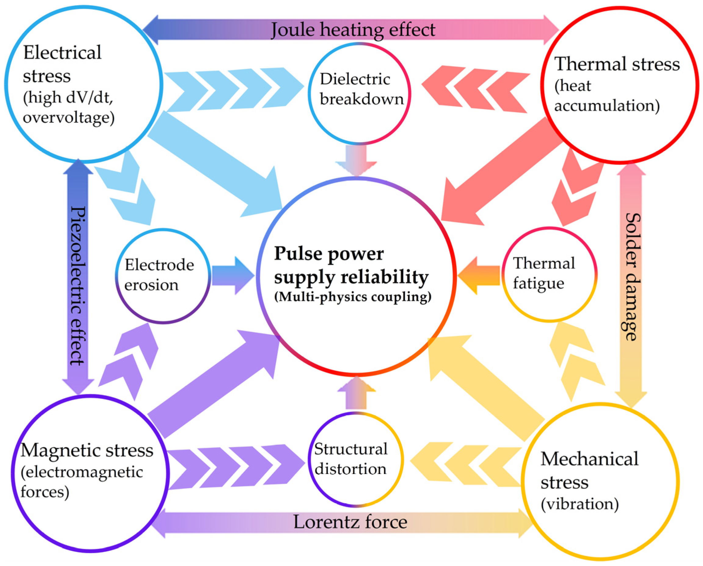
Figure 1. Schematic diagram of a typical pulsed power supply system structure [13,14,15].
Energies 19 00518 g001
Figure 2. Schematic diagram illustrating the multi-physics coupling effects in a pulsed power supply, showing the inter-related stress fields and resulting failure modes.
Energies 19 00518 g002
Figure 3. Theoretical analysis of capacitor durability under different operating conditions: (a) Influence of temperature on normalized lifetime degradation at unity voltage stress, (b) Impact of voltage stress on normalized lifetime degradation at 30 °C [32].
Energies 19 00518 g003
Figure 4. Key steps in the degradation and failure mechanism of the pulsed power capacitor.
Energies 19 00518 g004
Figure 5. Comparative analysis of key material properties for Silicon (Si), Gallium Nitride (GaN), and Silicon Carbide (SiC) [99].
Energies 19 00518 g005
Figure 6. Thermal behavior of the semiconductor switch core under pulsed operation [105]: (a) Comparison of the core and back temperature profiles during repetitive pulse sequences. (b) Transient temperature trend of the switch core under a single pulsed event.
Energies 19 00518 g006
Figure 7. Schematic of the AGD for dynamically regulating the drive current [123].
Energies 19 00518 g007
Figure 8. Resonant auxiliary drive circuit [124].
Energies 19 00518 g008
Figure 9. Overall framework for thermal management design across different hierarchical packaging levels [138].
Energies 19 00518 g009
Figure 10. Key considerations and trade-off metrics for selecting the optimal cooling technology in pulsed power systems [154].
Energies 19 00518 g010
Figure 11. The fundamental EMI model illustrating the source–path–receptor relationship [168].
Energies 19 00518 g011
Figure 12. Environmental stressors and reliability challenges for pulsed power systems deployed in marine applications [189,190,191,192].
Energies 19 00518 g012
Table 1. Classification of Pulsed Power Energy Storage Elements based on Storage Medium.
Energy Storage TypeEnergy Storage FormLifetimeInfluencing FactorsReferences
Capacitive storageElectric fieldHigh cyclic stability and longevityOvervoltage and overheating lead to material denaturation and lifetime reduction[23,24]
Inductive storageMagnetic fieldExceptional longevity and minimal inductive lossHigh voltage and current handling requirements for switching elements.[25,26,27]
Flywheel energy storageKinetic energyExtended service life, requires periodic maintenanceLimited by bearing friction and rotor fatigue[28,29,30]
Table 2. Summary of characteristic failure mechanisms for various capacitor types.
Capacitor TypeCharacteristic Failure MechanismsReferences
Polymer film capacitorsDielectric breakdown
Thermal accumulation causes dielectric aging and breakdown
[36,37,38]
Ceramic capacitorsDielectric breakdown
Thermal shock cracking
[39,40,41]
Electrolytic capacitorsElectrolyte evaporation
Oxide film degradation and breakdown
[42,43]
Table 3. Comparative Analysis of Characteristic Failure Mechanisms and Operational Lifetimes for Major Pulsed Power Switch Categories.
Switch CategoryRepresentative DevicesCharacteristic Failure MechanismsReferences
Plasma switchGas spark gap switch
Thyratron
Electrode melting and vaporization
Particle splashing
[81,82,83]
Semiconductor switchSiC MOSFETs, GaN HEMTs
Photoconductive switches
High dV/dt
Pulsed short-circuit
Severe overcurrent
Irreversible electrode degradation
Excessive or uneven optical excitation energy
[84,85,86]
Vacuum switchTriggered vacuum switchDegradation of Vacuum Integrity
Contact Erosion and Wear
[87,88]
Table 4. Suitability of Various Thermal Management Technologies for Different Pulsed Power Topologies [140,153,155,156].
Cooling MethodSuitable for Hierarchical LevelsCore StrengthsLimitationsHeat Transfer Coefficient (W/m2K)High Heat Flux (W/cm2)
Forced air coolingSystem-levelLow cost,
Simple structure,
Large heat dissipation surface area
Limited heat dissipation capacity,
High noise
Dust accumulation
2~2510~35
Thermoelectric coolingDevice-level
Board-level
Compact system-level
Precise temperature control,
High reliability
Low efficiency, Self-generated heat degrades output parametersNot applicable1~10
Immersion coolingDevice-level
Board-level
High heat dissipation capacity,
Compact structure,
Low noise
System complexity and risk of leakage50~100050~70
Microchannel coolingDevice-level
Board-level
Compact volume
Rapid transient response
High cost
High pressure drop
100~20,000100~1000
Two-phase immersion coolingDevice-level
Board-level
System-level
Excellent heat dissipation,
Excellent temperature uniformity, Strong environmental adaptability,
Low noise
High cost
Complex structure
Poor Maintainability
2500~100,00050~100
Table 5. Comparative analysis of technical characteristics, jitter precision, and scalability for different triggering methods.
Triggering MethodTechnical CharacteristicsJitter PrecisionScalabilityCostReference
Electrical triggeringBased on corona stabilized triggered switch3.1–4.8 nsLowLow[159]
Cascaded amplification architecture: comprises an 8-channel digital delay generator (DDG), a pulse generator (PG), and a compact low-inductance Marx generator.<2 nsHighMiddle[160]
FPGA timing control and magnetic ring transformersJitter depends on FPGA clockHighMiddle[161]
All-solid-state design, primary windings on individual cores; secondary winding encloses all cores, functioning as the Marx circuit magnetic switch0.64–2.53 nsHighMiddle[162]
FPGA timing control combined with a compensation circuit consisting of an active gated integrator and an output comparatorPicosecond levelHighhigh[163]
Optical triggeringCascaded amplification architecture and high-power ultraviolet laser<1 nsHighVery high[164]
Combining DC bias avalanche photoconductive semiconductor switch (PCSS) and spark gap switch<3 nsHighMiddle[165]
Table 6. Comparison of reliability characteristics of four representative PPS topologies [175,176,177,178,179,180].
PPS ArchitectureOperational CharacteristicsCritical ComponentsMain Failure MechanismsMitigation Strategies
Marx generatorHigh-voltage pulsed output
High efficiency
Flexible parameter adjustment
Switch
Energy storage elements
Dielectric aging
Switch Electrode Erosion
Synchronization-induced Overvoltage
Electrode material and cooling optimization
Low-jitter trigger system
Linear transformer driver (LTD)High efficiency
High power density
Modular scalability
Magnetic Core
Winding
Switch
Capacitance
Magnetic core loss and heating
Dielectric breakdown
Winding deformation
High-frequency low-loss magnetic material and liquid cooling
Optimization of winding mechanical fixation
Pulse Forming Network (PFN)Precise pulse waveform control
Low system complexity
High load adaptability
Inductance
Capacitance
Switch
Breakdown of capacitors and inductors
Component overvoltage Breakdown
Overvoltage and Overcurrent protection
Improved thermal management strategies
Blumlein Pulse Forming Line (BPFL)Excellent pulse quality
High voltage efficiency
Switch
Blumlein transmission lines
Overcurrent-induced Switch breakdown
Dielectric breakdown of transmission line
Addition of switch snubber circuit
Table 7. Overview of environmental stressors, dominant failure mechanisms, and targeted mitigation strategies for pulsed power systems.
ScenarioEnvironmental StressorsDominant Failure MechanismMitigation Strategy
AerospaceVacuum
High-energy radiation
Surface flashover
Thermal accumulation
Oxide layer damage
Radiation-hardened design
Derating usage
NavigationHigh humidity
High salinity
Thermal cycling
Reduction in insulation resistance
Solder joint fatigue
Coating design
Advanced soldering technology
DesertLong-term high temperature
Sand interference
Thermal feedback loop caused by dust blockage and solar heatHigh-temperature resistant design
Hermetic sealing
Disclaimer/Publisher’s Note: The statements, opinions and data contained in all publications are solely those of the individual author(s) and contributor(s) and not of MDPI and/or the editor(s). MDPI and/or the editor(s) disclaim responsibility for any injury to people or property resulting from any ideas, methods, instructions or products referred to in the content.