


Abstract
A Controllable Line-Commutated Converter (CLCC) is a novel piece of equipment for enhancing the commutation failure resistance of High-Voltage Direct Current (HVDC) transmission systems. Traditional lumped parameter models ignore the high-frequency coupling effects of internal distributed stray capacitances, resulting in insufficient transient simulation accuracy and restricting refined engineering design. Taking the CLCC in the HVDC transformation project as the research object, this paper analyzes the distribution characteristics of stray parameters in a press-pack Insulated Gate Bipolar Transistor (IGBT) under stacked structures. By integrating distributed stray parameter networks with the nonlinear characteristics of the devices, an improved IGBT equivalent circuit model is established, with key parameters identified based on field-measured data. Furthermore, an LCC-CLCC simulation model is built and used to replace the improved IGBT model to conduct short-circuit fault simulation verification. The results demonstrate that the high-fidelity model accurately reproduces transient waveforms under Alternating Current (AC) voltage disturbance and faithfully reflects the actual operating characteristics of a surge arrester and IGBT, thereby effectively compensating for the idealized errors inherent in traditional models. This modeling methodology provides a robust theoretical and simulation foundation for parameter optimization, valve control system design, and the secure operation of a CLCC.
1. Introduction
Against the backdrop of the rapid development of the Global Energy Interconnection and the transformation toward new-type power systems, HVDC transmission has emerged as a pivotal technology for large-capacity, long-distance energy transmission and cross-regional asynchronous interconnection [1,2]. As the structure of the multi-infeed DC (MIDC) receiving grid becomes increasingly complex, conventional Line-Commutated Converters (LCCs) are prone to commutation failures under weak AC system conditions, causing the power grid to operate unstably [3,4,5,6,7,8,9]. The CLCC integrates an IGBT-based auxiliary branch into the traditional thyristor valve to achieve active regulation of the commutation process. This suppresses commutation failure from a topological mechanism perspective, significantly enhancing the fault ride-through capability and operational stability of the DC [10,11]. Currently, the first CLCC has been put into operation on the China Shanghai power grid in June 2023. Field operation results have verified that it achieves controllable commutation during AC system faults, effectively resisting commutation failures and weakening the power disturbances caused by such events [12,13,14,15,16]. However, research into CLCC modeling and characteristic analysis indicates that theoretical models based on traditional lumped parameters fail to accurately reproduce measured transient waveforms. The fundamental cause of this deviation between theoretical simulation and actual physical characteristics lies in the inherent models’ neglect of the high-frequency coupling mechanisms induced by internal spatially distributed stray capacitances.
During the high-frequency switching transients of IGBT, stray parameters trigger a significant voltage peak, current oscillations, and issues with dynamic voltage and current imbalance [17,18], which are critical factors limiting the safe operation of the devices. Due to the inadequate characterization of high-frequency transient mechanisms in traditional simulation models, non-physical discrepancies exist between simulation results and field-measured data. It is difficult to support the refined design of CLCC overvoltage protection, voltage and current balancing strategies, and valve-controlled systems.
The modeling deviations mentioned above undermine the accuracy of electrical and thermal stress assessments for the internal CLCC surge arrester and IGBT, potentially leading to a lack of scientific basis for the parameter design of key components. Such uncertainty further constrains the overall performance optimization of the converter valve and the refined study of critical parameters. Consequently, there is an urgent need for an in-depth investigation into the characteristics of key components under the influence of distributed stray capacitances.
Regarding this critical scientific issue, scholars both domestically and internationally have made significant progress in power device modeling, stray parameter extraction, and the impact of stray capacitance. In terms of power device modeling, reference [19] proposed a high-frequency parasitic model for IGBT power modules by constructing a behavioral model of the IGBT chip embedded in a parasitic parameter network, utilizing static characteristics and Finite Element Method (FEM) extraction results. Reference [20] proposed an optimization scheme based on the distribution characteristics of internal parasitic inductance; after optimization, both the parasitic inductance and turn-off overvoltage within the IGBT module were significantly reduced. Some studies have employed the Partial Element Equivalent Circuit (PEEC) method and 3D electromagnetic simulation to achieve precise extraction of power circuit stray parameters. Reference [21] presented a rapid extraction method for power module layout inductance based on a multi-port network model. Reference [22] studied the impact of different integration intervals on the accuracy of stray inductance extraction and chose to calculate the stray inductance in the integration interval with smaller errors. By performing polynomial fitting on the voltage and current, the functional expressions of voltage and current were obtained, which were then substituted into the calculation formula of stray inductance to calculate the stray inductance under the influence of different parasitic capacitances. Reference [23] proposes a multi-parameter extraction method for parasitic inductance based on the LC high-frequency oscillation principle, fully utilizing the converter’s own structure. Through three field experiments, different resonant circuits are actively constructed, and the parasitic inductances at different positions of the converter are calculated based on their oscillation frequencies. Regarding the impact of stray capacitance, reference [24] conducts research on the issue of abnormally high readings of bridge differential protection ammeters for AC filter capacitors in high-voltage direct current (HVDC) transmission projects. Reference [25] noted that stray capacitance between measurement equipment and the converter valve leads to inaccurate test voltage measurements, calculating these capacitances and establishing a simulation model based on the test circuit parameters.
At present, research on high-frequency switching transient and its induced effects is largely concentrated in the field of fast-switching wide-bandgap devices such as those made from Silicon Carbide (SiC) [26,27,28,29]. In contrast, systematic research on the transient characteristics and distributed parameter effects within large-scale HVDC converter valves remains relatively scarce [30]. It is traditionally assumed that, due to the lower switching frequency and slower switching rate (dv/dt and di/dt) of large-scale HVDC valves, the probability of switching transients exciting significant distributed effects is low. However, in the novel valve structure and actual operating conditions investigated in this paper, the coupling between local switching characteristics and the spatial distribution parameters of the valve tower has led to non-negligible transient issues.
This paper is based on the actual physical structure of the controllable commutation converter valve in DC retrofit projects, and carries out detailed modeling research on the series-parallel circuit characteristics of its press-pack IGBT. We conducted an in-depth analysis of the physical distribution characteristics under the CLCC stacked structure, and extracted the key parasitic parameters affecting the device dynamic processes. Based on basic components, such as resistors, inductors, and capacitors, we constructed an improved IGBT equivalent circuit model that can represent parasitic effects. We performed parameter identification and experimental verification of the model using steady-state and transient voltage and current data measured on-site. The main content of this paper is organized into several parts as follows. Section 2 analyzes the distribution characteristics of stray parameters in CLCCs and develops an improved equivalent circuit model of the press-pack IGBT incorporating distributed parasitic effects. Section 3 establishes the LCC–CLCC simulation model and presents the validation results under AC voltage disturbances based on field test data. Section 4 provides a detailed discussion on the modeling accuracy and its engineering implications. Finally, Section 5 summarizes the main conclusions of this work.
This paper develops a high-fidelity modeling framework for CLCCs that integrates distributed stray parameter effects into an improved IGBT model, achieving accurate transient simulation and providing reliable support for the engineering design and operation of HVDC systems.
2. Materials and Methods
2.1. Analysis of Stray Parameter Distribution Characteristics in CLCC
2.1.1. Connection Structure of IGBT in CLCC
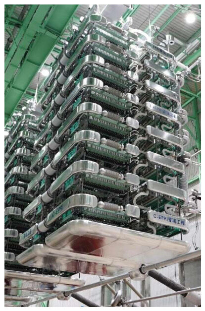
In the HVDC retrofit project, the CLCC adopts a single-valve modular design, wherein each valve module consists of a main branch and an auxiliary branch connected in parallel. The overall physical assembly employs an eight-layer stacked structure. Each layer comprises key components, including power devices, grading resistors, snubber capacitors, and connecting busbars. To ensure high-voltage insulation performance, adjacent layers are separated by insulating barriers. The eight-layer stacked structure of the CLCC is shown in Figure 1.
Figure 1.
Eight-layer stacked structure of the CLCC.
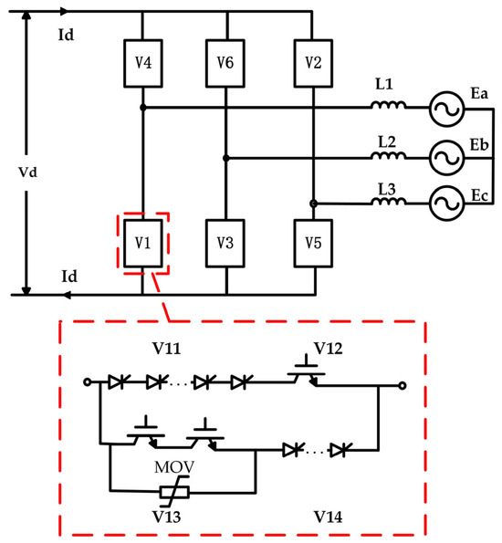
The main branch features a series-connected structure of thyristor and press-pack IGBT to undertake primary power transmission. The auxiliary branch, comprising series-parallel press-pack IGBT modules, facilitates active regulation of the commutation process by outputting compensation current to modulate the commutation voltage and suppress commutation failure.
Considering the working voltage level of the converter valve and the power transmission requirements, both the main branch and auxiliary branch of a single valve adopt multiple pressed-type IGBT series configurations. The structural topology is shown in Figure 2.
Figure 2.
Structural topology of the CLCC.
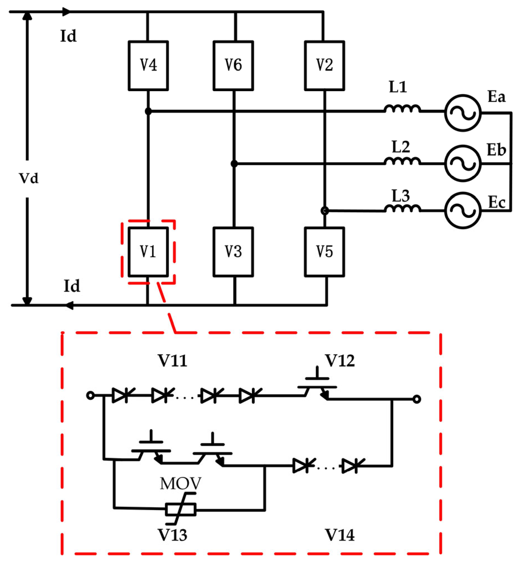
Press-pack IGBTs utilize a ceramic packaging structure, offering superior thermal dissipation, high mechanical strength, and excellent high-voltage capability. However, the packaging and stacked layout inevitably introduce stray parameters. Compared to conventional IGBTs, press-pack variants feature more complex electrode connections, housing, and inter-layer insulation. These factors lead to more pronounced nonlinear distribution characteristics of stray parameters, significantly impacting high-frequency switching transients. The specific internal valve topology reflecting these characteristics is shown in Figure 3.
Figure 3.
Detailed topology of the IGBTs.
The figure above presents a detailed topology of the IGBTs in the V12 and V13 sections within the valve. This module topology clearly illustrates the IGBT structures in both the main branch and the auxiliary branch. Through a detailed depiction of the electrical connections of the internal components, it can be observed that the complex electrode leads of press-pack IGBTs, together with the spatial layout of the converter valve tower, constitute the fundamental physical sources of nonlinear distributed stray parameters.
2.1.2. Sources of Stray Parameters in CLCC
Stray parameters within the CLCC primarily come from device packaging, power circuit layout, interlayer connections, and auxiliary components. These are categorized into stray inductance, stray capacitance, and mutual inductive coupling based on their physical nature. Stray inductance arises from conductive parts such as power busbar, IGBT electrode lead, and grading resistor connection; its magnitude is closely related to conductor length, cross-sectional dimensions, arrangement, and surrounding dielectric properties. Parasitic capacitance mainly exists between the IGBT chip and the package casing, between interlayer conductors and insulating partitions, and between power devices and grounding structures. It belongs to distributed capacitance, with a wide distribution range and uneven values. Mutual inductive coupling stems from electromagnetic induction between different power branches and stacked units, occurring mainly between adjacent IGBT series-parallel units of the main branch and auxiliary branch, which leads to transient stress interference between branches.
Owing to the stacked structure of the CLCC, stray parameter distribution exhibits distinct layering characteristics. Top and bottom units are influenced by grounding structures, resulting in relatively large stray capacitances. Middle units maintain relatively stable stray inductance and mutual coupling due to a more uniform electromagnetic environment. The coupling effect of stray parameters between the main branch and auxiliary branch is the most significant, and is the primary cause of voltage and current oscillations during the commutation process. Additionally, contact resistance between the chip and electrodes of press-pack IGBTs, along with internal parasitic inductance, significantly affects switching transients and must be considered during parameter extraction.
As a core component of HVDC transmission systems, the CLCC features a highly complex and repetitive physical structure. To investigate its internal transient evolution processes, this paper abstracts the complex physical entity into a generalized distributed-parameter network, as shown in Figure 4, based on the laminated distribution characteristics of the converter valve and the electrical topology of its power busbars.
Figure 4.
Complex circuit diagram.
It should be noted that the branch parameters in Figure 4 do not correspond one-to-one with the geometric structure of the converter valve. Instead, they represent a classification and topological aggregation of the physical sources of stray effects in the power circuit, voltage equalization circuit, and interlayer insulation structure. This abstraction approach enables the transformation of electromagnetic coupling relationships in physical space into circuit models that are convenient for computation. In practical modeling processes, any complex converter valve structure can ultimately be transformed into an equivalent schematic by following this logic.
To accurately obtain the internal stray parameters of the CLCC while balancing simulation accuracy and computational efficiency, this paper further simplifies the distributed-parameter network shown in Figure 4 into a lumped-parameter equivalent model, as shown in Figure 5.
Figure 5.
Simplified circuit diagram.
By decomposing the complex laminated structure into multiple basic units and calculating inductance, capacitance, and mutual inductance, a stray-parameter equivalent circuit model is established, thereby enabling quantitative extraction.
2.2. Improved Equivalent Circuit Modeling of IGBTs Considering Stray Effects
2.2.1. Limitations of Conventional IGBT Models
Current electromagnetic transient simulations of power systems primarily include three types of IGBT equivalent models: ideal switch, simplified behavioral, and physical-level models. The ideal switch model ignores the device’s conduction voltage drop, switching losses, and parasitic parameters, representing only the on/off logic of the device and failing to reflect its high-frequency transient characteristics. Simplified behavioral models incorporate basic parameters like conduction resistance and junction capacitance. While these can reflect conduction losses and switching actions to some extent, they neglect distributed stray parameters and mutual inductive coupling induced by press-pack packaging, making it difficult to accurately characterize voltage peak and current oscillation during high-frequency switching. The physics-level model is based on the carrier transport mechanisms within the device and offers high simulation accuracy. However, its complex structure, numerous parameters, and substantial computational load make it difficult to apply to the simulation of complex systems such as the CLCC, which involve multiple devices in series and parallel.
At present, in electromagnetic transient simulation software such as PSCAD, the built-in IGBT models are mostly ideal switch models or simplified behavioral models. The main limitation of these models lies in their high level of simplification: they only possess basic turn-on and turn-off logic, behaving essentially as ‘variable switches’ whose resistance changes with control signals during simulation. They neglect the complex carrier transport processes within the device as well as the microscopic parasitic parameters introduced by packaging, and thus are unable to reproduce the voltage and current dynamic responses during high-frequency switching transients. This highly idealized treatment leads to the inability of the models to accurately capture stray oscillations induced by AC voltage fluctuations when simulating complex commutation processes involving large numbers of series and parallel devices, such as in CLCC systems. As a result, the simulated waveforms appear overly smooth, losing their practical reference value for overvoltage protection design and voltage balancing strategy studies in real engineering applications.
To overcome the aforementioned limitations, a user-defined IGBT component model is developed in the PSCAD environment. Compared with the built-in models that only provide ‘switching functionality,’ this model offers the following significant advantages:
- Reproduction of nonlinear transients: By embedding the extracted distributed stray-parameter network of , , and around the core switching logic, the model is able to capture the intrinsic characteristics of the IGBT, rather than representing it as a simple step change.
- Balance between accuracy and efficiency: The model avoids the extremely high computational complexity of physics-based models, while faithfully reproducing the actual operating characteristics of press-pack IGBTs through a user-defined interface. It effectively eliminates the ‘idealization error’ present in traditional models and provides reliable theoretical support for the design of CLCC valve control systems.
2.2.2. Derivation of the Improved Equivalent Circuit Model
The improved equivalent circuit model for press-pack IGBT mentioned in this paper is based on the simplified behavioral model, integrated with a distributed stray parameter network and nonlinear device characteristics to achieve higher simulation fidelity.
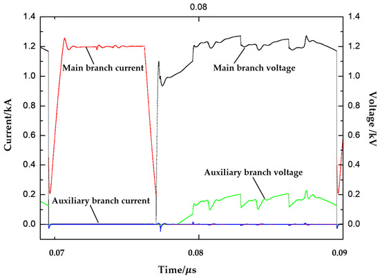
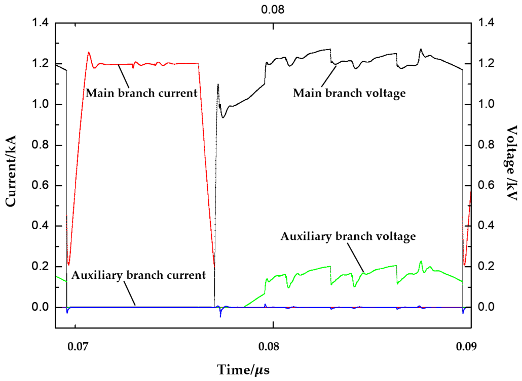
To verify the accuracy of the improved equivalent circuit model, this research conducted operational tests using a full-scale CLCC test valve to obtain the voltage and current data of the IGBT during operation, as shown in Figure 6 and Figure 7.
Figure 6.
Steady-state voltage and current waveforms.
Figure 7.
Transient voltage and current waveforms.
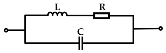
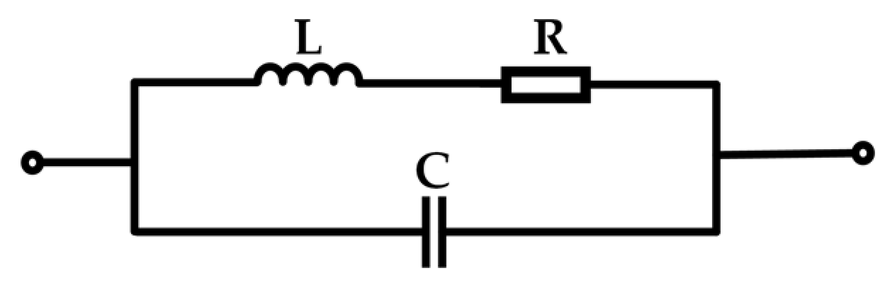
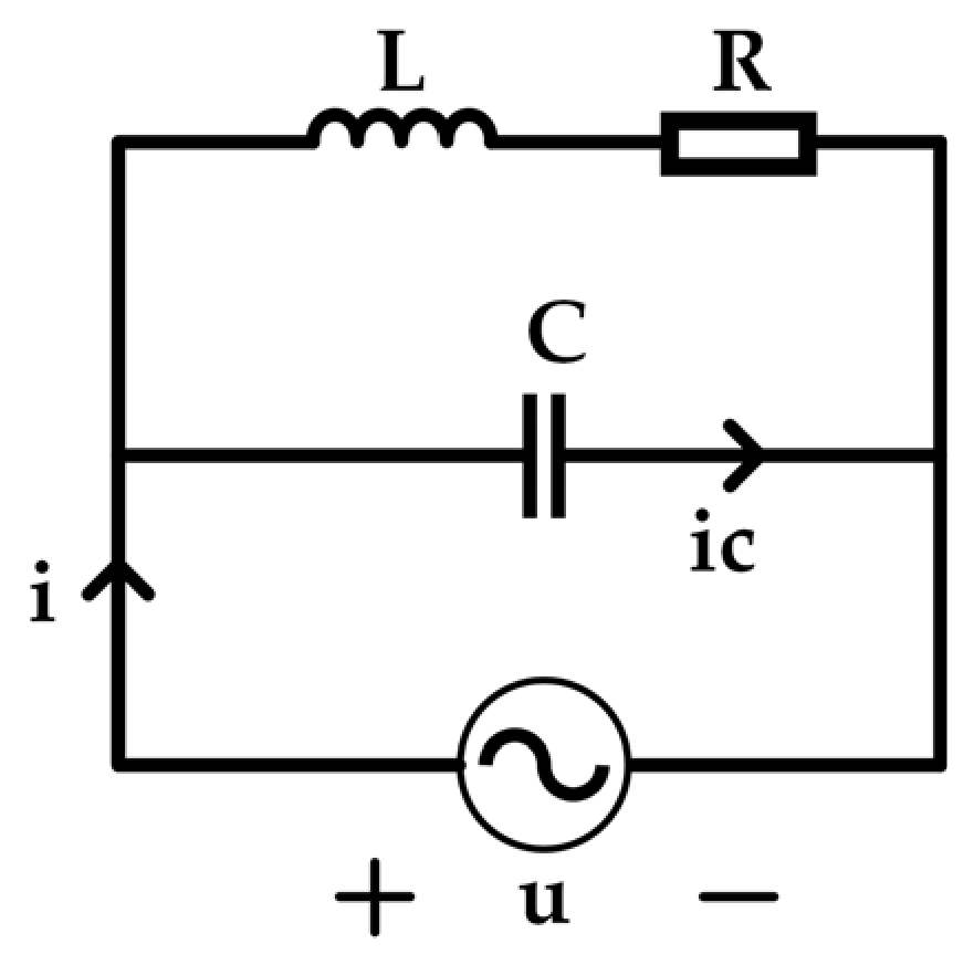
As shown in Figure 6, during the natural commutation process, the current decreases more slowly compared to the voltage variation, indicating that the inductance in the circuit is non-negligible; the voltage fluctuations of the auxiliary branch show a certain correlation with the voltage waveform of the main branch IGBT. This is based on the analysis in the previous section, and considering the electrical connection structure and spatial distribution of the IGBT, especially in cases where the auxiliary branch IGBT experience overvoltage. A refined electrical model of the IGBT is proposed as shown in Figure 8.
Figure 8.
Refined electrical model of the IGBT.
According to the circuit principle, during the natural commutation process, the surge arrester typically remains inactive. Consequently, it can be roughly regarded as a characteristic of the auxiliary branch itself. Based on the established circuit model, the fundamental governing equations are derived as follows:
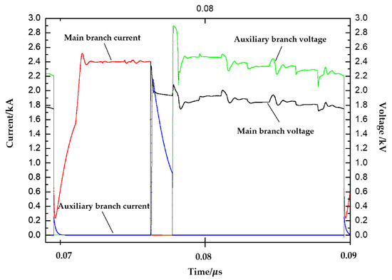
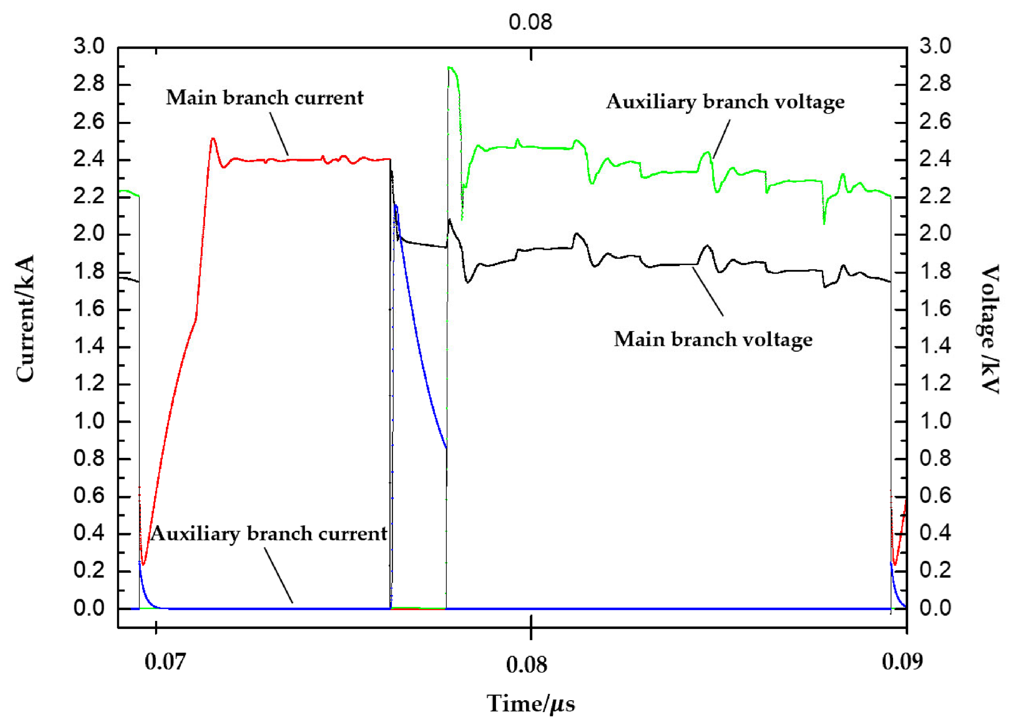
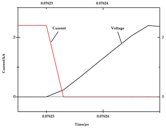
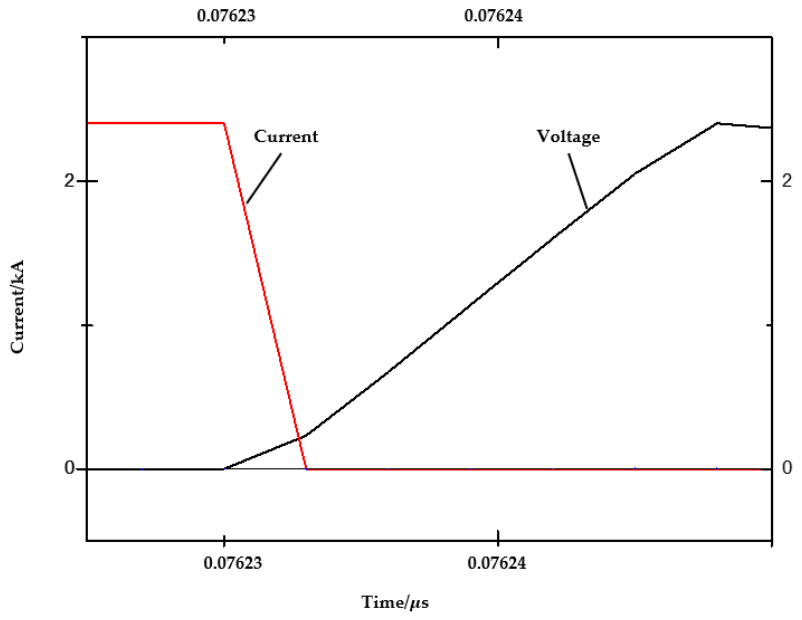
The data from the field short-circuit test are analyzed and fitted. Zoom in on the IGBT voltage and current during the transient process, and also enlarge Figure 7 to observe the voltage and current changes during the IGBT turn-off. The detailed enlarged view is shown in Figure 9 below.
Figure 9.
Enlarged view of IGBT voltage and current.
To simplify the fitting, we divide the turn-off process into two stages for parameterization.
The first stage is the rapid current fall period; in this stage, the current rapidly drops from its steady-state value to 0, resulting in a large slope of . At this moment, just begins to rise. Neglecting the smaller and terms, the voltage spike is mainly caused by the inductance, satisfying:
Select the linear segment where the current decreases most rapidly (with approximately constant). Read the corresponding voltage and current at this moment. Typically, the effect of is small in this stage, so can be preliminarily estimated using:
where is the voltage spike, measured in kV; and is the average current during the current falling interval, measured in kA.
Based on the above analysis, the value of can be obtained.
The second stage is the voltage tailing and oscillation period; this stage occurs after the current has completely decayed to 0. The equation becomes:
This is a typical exponential decay or transient process. Extract the voltage waveform segment after the current has decayed to zero. Perform a first-order linear fitting of the voltage over this segment. Using the instantaneous moment just before the current fully decays to zero, the value of can be obtained from Equation (5).
During the voltage rising phase or the initial stage after the current has decayed to zero, can be determined using Equation (1).
The corresponding , , and parameters are deduced based on the IGBT’s turn-on and turn-off characteristics.
The specific values are as follows:
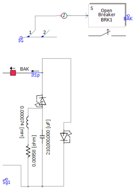
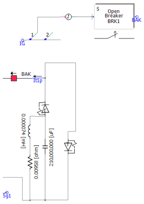
Additionally, the IGBT core nonlinear equivalent module is used to characterize the device’s dynamic behaviors, including turn-on, turn-off, and reverse recovery. This module uses diodes and timing logic blocks, and introduces a switching control function to simulate the switch conduction.
To achieve accurate simulation of the internal transient processes of the CLCC under AC voltage disturbances, when modeling the high-frequency transient processes of the CLCC, the implications of time delays and device consistencies cannot be overlooked. The overall switching delay in practical applications is primarily composed of two parts: the delay introduced by the gate driver circuits and the intrinsic delay of the IGBT power transistor itself. The proposed component is designed in accordance with the operating logic of IGBTs, and can be described from two aspects.
In terms of control logic, the switching operation of the component is strictly governed by the firing angle command (IG) issued by the internal valve control system. The control logic unit receives the IG signal in real time and converts it into corresponding high- and low-level pulses according to the given timing sequence. Combined with monitoring the voltage polarity across the device, a conduction signal is generated only when a trigger pulse is received and the device is under forward bias. When forced current interruption is required during transient processes, the trigger signal is withdrawn, and the logic unit immediately issues a turn-off command to enforce current commutation.
At the topological level, due to the limited reverse blocking capability of conventional IGBTs, auxiliary diodes are incorporated into the custom module. Two diodes are employed in total: an anti-parallel diode, which provides a freewheeling path, dissipates the energy stored in stray inductance during high-speed turn-off of the IGBT, and suppresses switching overvoltage; and a series diode, which provides high-frequency reverse blocking capability, preventing device breakdown when reverse bias occurs due to AC-side voltage.
Based on the above analysis, the user-defined component can be constructed as shown in Figure 10.
Figure 10.
User-defined component model.
By integrating the aforementioned stray parameter extraction results with the IGBT core nonlinear module, the user-defined component model can more realistically simulate the dynamic behaviors of power devices during turn-on and turn-off transients. Compared with traditional ideal switch models, this improved model provides critical modeling support for reproducing voltage spikes and current oscillations under high-frequency transient processes in the PSCAD simulation environment. This refined modeling approach is an essential prerequisite for enhancing the electromagnetic transient simulation accuracy.
3. Results
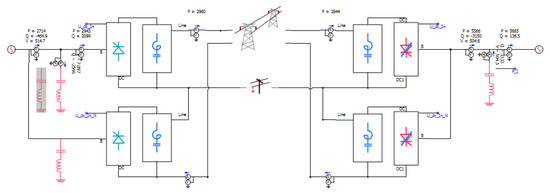
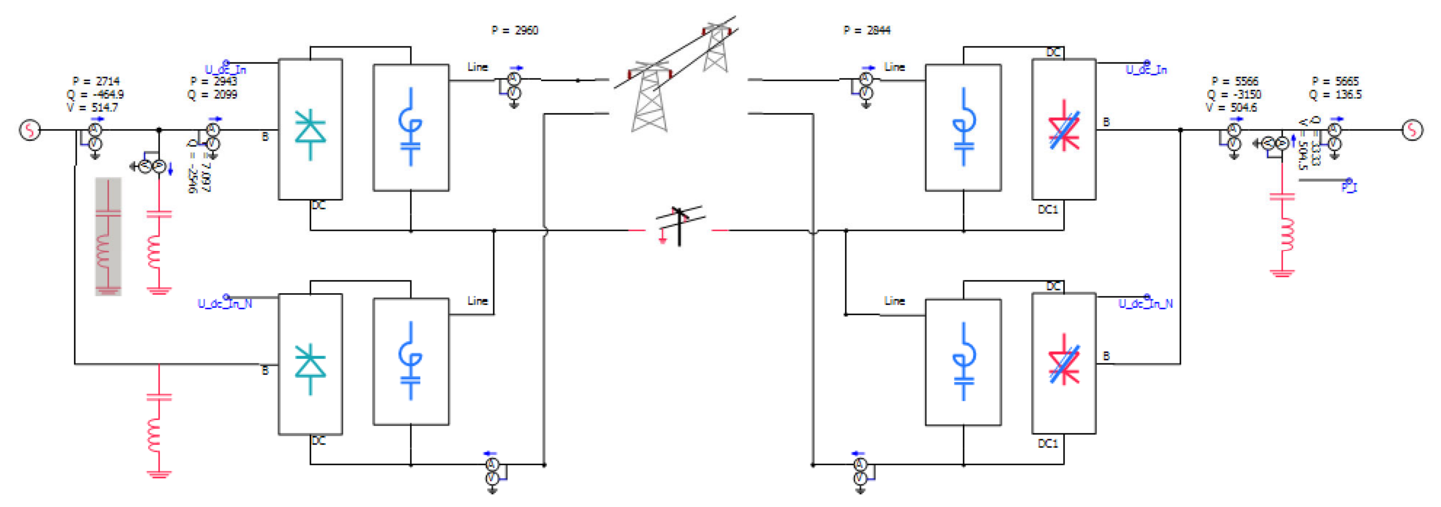
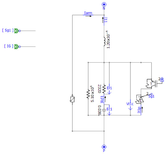
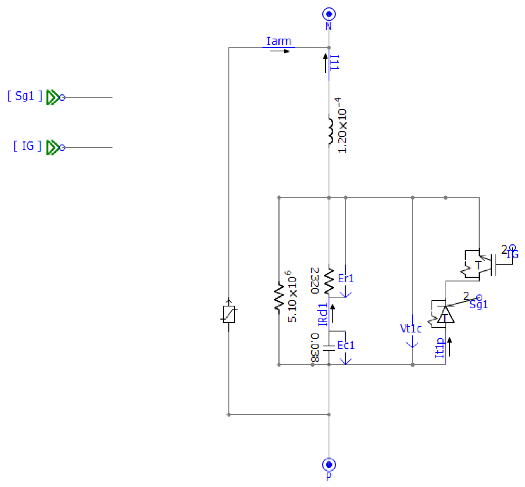
To verify the effectiveness of the user-defined component model, an electromagnetic simulation model of an AC-DC system was built using PSCAD 5.0.0. The system configuration consists of an LCC at the sender and a CLCC at the receiver. The LCC-CLCC simulation model is shown in Figure 11.
Figure 11.
LCC-CLCC simulation model.
Figure 12.
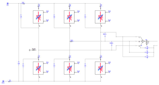
Internal structure diagram of the valve.
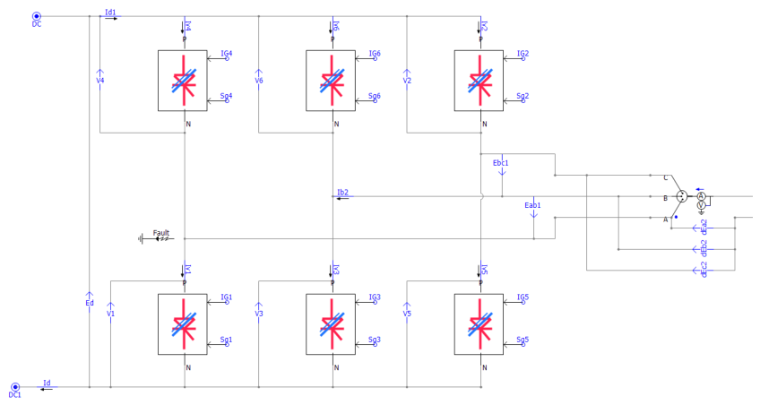
Figure 13.
Internal bridge arm structure diagram.
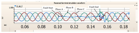
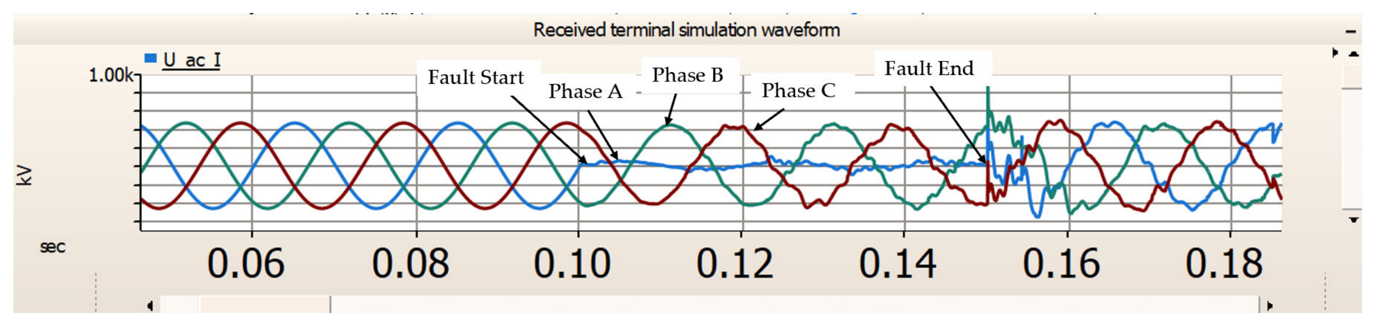
To verify the correctness of the established LCC–CLCC simulation model, in the LCC-CLCC simulation model, a single-phase-to-ground fault is applied to phase A. The fault is initiated at with a duration of . The resulting simulated voltage waveforms are illustrated in Figure 14.
Figure 14.
Simulated grid-side voltage waveforms during a Phase-A-to-ground fault.
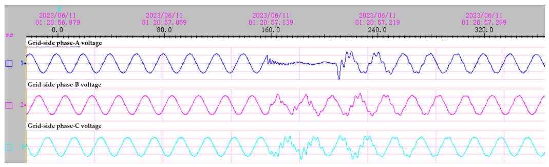
Utilizing the field test of the CLCC for the DC transformation project, an artificial short-circuit test was conducted to measure a Phase-A-to-ground fault. The corresponding recorded voltage waveforms on the grid side are shown in Figure 15.
Figure 15.
Recorded grid-side voltage waveforms during a Phase-A-to-ground fault.
A comparison between the simulation waveform in Figure 14 and the measured voltage recording in Figure 15 shows a high degree of consistency in terms of waveform shape, amplitude variation, and fault evolution trend. This agreement indicates that the established LCC–CLCC simulation model is capable of accurately capturing the dynamic response characteristics of the AC system under voltage disturbance conditions, particularly the transient behavior during the initiation and development of a single-phase-to-ground fault.
However, it should be noted that this consistency is mainly reflected at the system level, such as the external grid-side voltage response. The internal electromagnetic transient processes within the converter valve, especially those related to the detailed switching behavior of power electronic devices and the influence of distributed stray parameters, are not sufficiently represented in the current model. As a result, the simulation still lacks the ability to reflect the fine-scale high-frequency interactions and internal coupling effects among components inside the valve.
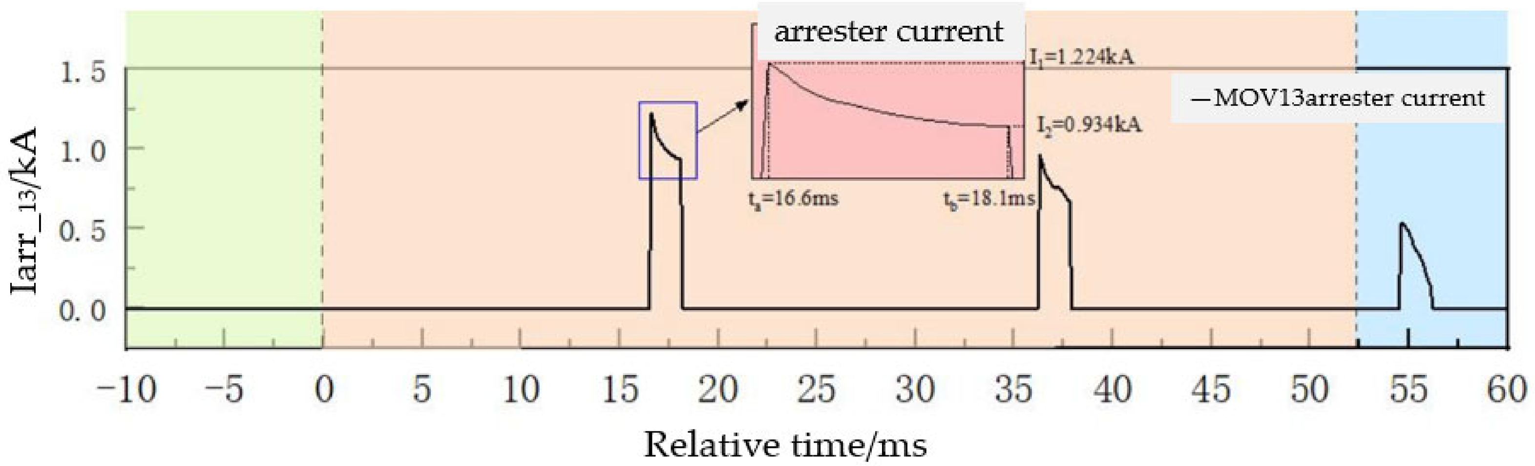
To further verify the modeling effectiveness of the user-defined components, the transient data from the artificial short-circuit test were extracted. It was observed that the surge arrester experienced continuous triggering during the voltage dip, as shown in Figure 16.
Figure 16.
Measured surge arrester current.
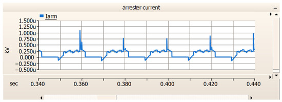
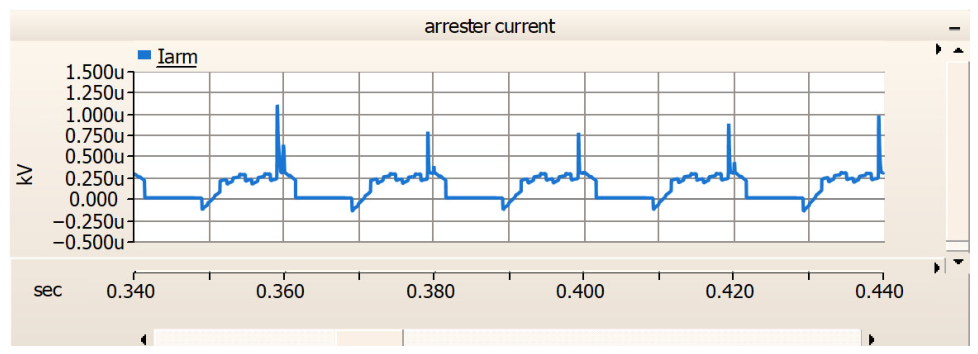
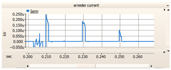
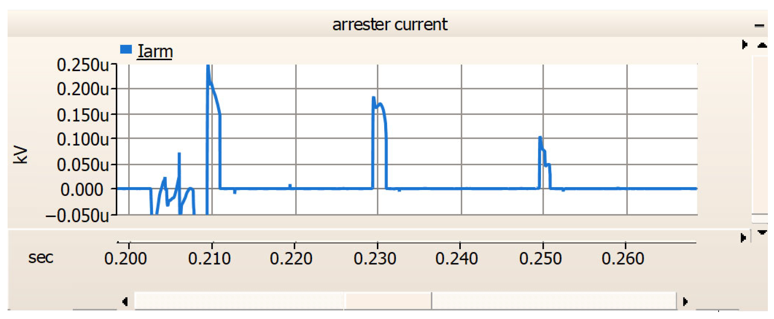
By replacing the original IGBT in Figure 13 with the user-defined components, the simulated arrester current waveforms exhibit certain differences compared with those of the pre-optimization model, as shown in Figure 17 and Figure 18.
Figure 17.
Surge arrester current with the original IGBT model.
Figure 18.
Surge arrester current with the user-defined component model.
By comparing the simulated arrester current in Figure 15 and Figure 16 with the field-recorded arrester current in Figure 14, it can be observed that the improved model more accurately reflects the actual operating conditions of the arrester. The simulated arrester current obtained using the traditional IGBT model shows significant deviations in amplitude and oscillatory characteristics from the measured data, failing to accurately reproduce the actual arrester behavior. In contrast, after replacement with the improved IGBT model, the simulated arrester current amplitude, pulse occurrence timing, and transient oscillation frequency all closely match the measured waveforms. This demonstrates that the improved model can accurately capture the transient overvoltage process within the valve and realistically reflect the arrester’s performance under AC voltage disturbances.
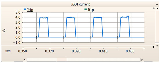
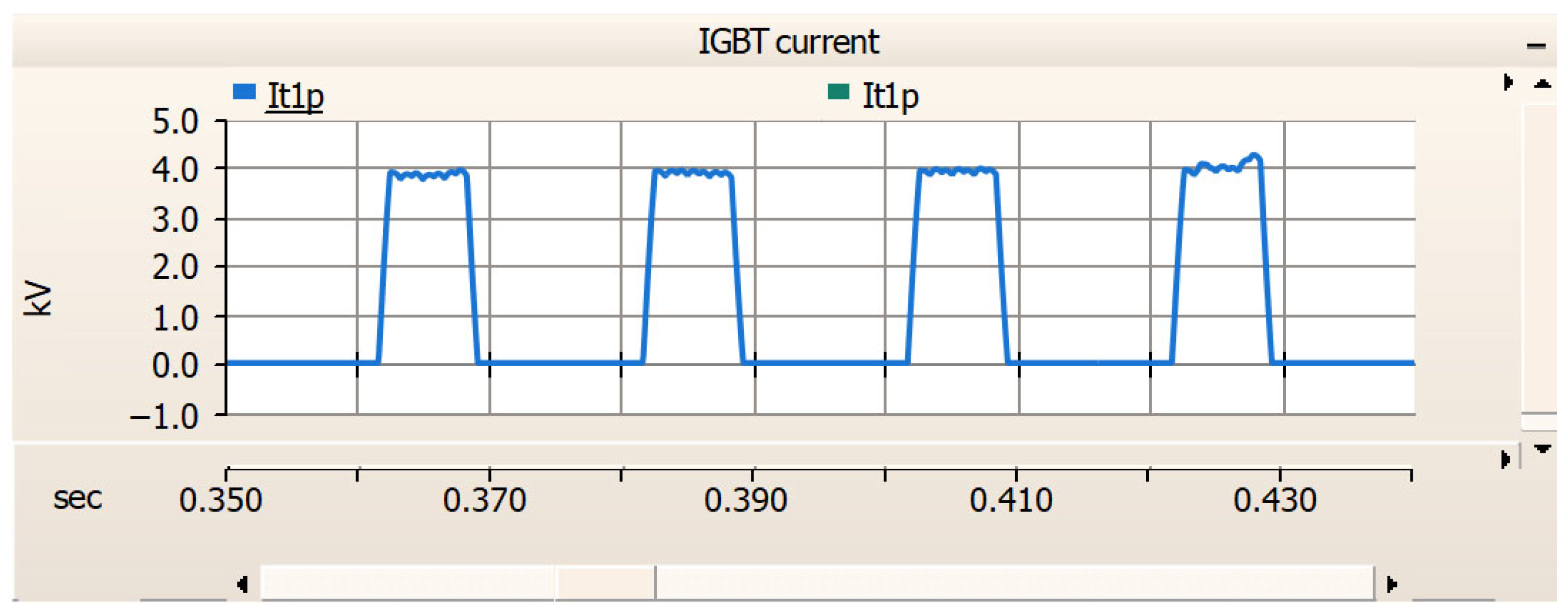
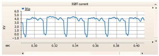
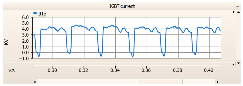
A comparison of the IGBT current before and after the model replacement is shown. It is evident that the improved model provides significantly richer high-frequency components during the conduction process, as shown in Figure 19 and Figure 20.
Figure 19.
IGBT current with the original simulation model.
Figure 20.
IGBT current with the user-defined component model.
During the simulation, current waveforms under identical operating conditions were closely monitored and recorded. The comparison indicates that the original model primarily relies on simplified ideal switching logic, which fails to adequately account for the nonlinear characteristics of practical power electronic devices during turn-on and turn-off transients. With the introduction of a custom IGBT component, the improved model more accurately reproduces switching transients, on-state voltage drops, and high-frequency dynamic responses. The resulting current waveforms show closer agreement with field measurements, effectively eliminating the idealization errors existing in the original model. Moreover, the improved model provides richer waveform details and significantly enhanced measurement accuracy, enabling a more precise and objective representation of the electromagnetic transient behavior of AC/DC systems under real operating conditions.
This research addresses the limitation of traditional lumped-parameter models in reproducing measured transient waveforms and identifies high-frequency coupling induced by spatially distributed stray capacitances as the primary cause of discrepancies between simulation and physical behavior. Experimental results show that the refined model accurately characterizes the electrical stress distribution of press-pack IGBTs at the device level, thereby filling the gap in the representation of high-frequency transient characteristics within large converter valves in existing research.
4. Discussion
- Traditional lumped-parameter models fail to accurately reproduce the measured transient waveforms under AC voltage disturbances, primarily because they neglect the high-frequency coupling effects of stray inductance, stray capacitance, and mutual inductance within the converter valve. The eight-layer stacked structure of the CLCC results in a distinct layered distribution of stray parameters, and the strong coupling between the main and auxiliary branches constitutes the main cause of voltage and current oscillations during commutation. Furthermore, the packaging characteristics of press-pack IGBTs further amplify the impact of stray parameters on switching transients, which must be emphatically considered in refined modeling. The IGBT model proposed in this paper integrates a distributed stray-parameter network and the nonlinear characteristics of the device, and identifies the key R, L, and C parameters based on field-measured data. Compared with ideal switch models and conventional behavioral models, the improved model can precisely characterize voltage spikes, current oscillations, and high-frequency dynamic responses without a significant increase in computational cost. It effectively remedies the deficiency of traditional models that disregard distributed parameters and mutual inductance coupling, thereby providing reliable support for the accurate evaluation of electrical and thermal stresses of key devices.
- Most existing studies focus on wide-bandgap devices, while systematic research on the distributed parameter effects of the CLCC remains insufficient. Based on practical engineering, this paper systematically reveals the distribution law and operating mechanism of stray parameters in the CLCC. The proposed modeling method can be extended to the design, simulation and operation analysis of similar controllable line-commutated converter valves, which is of great engineering significance for improving the commutation failure immunity of HVDC transmission systems.
- After embedding the customized improved IGBT component into the established LCC-CLCC model, the waveforms of grid-side voltage, arrester current, and IGBT current under a single-phase grounding fault are highly consistent with field measurements. The refined model can truly reflect the actual operating characteristics of arresters and IGBTs, eliminate the idealization errors of conventional models, and provide effective simulation support for the design of valve control systems and the formulation of overvoltage protection strategies.
- It should be noted that the current validation is based on single phase-to-ground fault data. Although the stray parameter network is extracted from the fixed physical structure of the CLCC and remains consistent under various operating conditions, more severe disturbances such as three-phase short circuits may trigger more complex coupling mechanisms. Future research will focus on evaluating the model’s robustness under a broader spectrum of fault scenarios to further enhance its engineering applicability.
- The refined model developed in this study, while validated against a specific eight-layer CLCC structure, offers a generalized framework for transient analysis. For applications involving alternative topologies or different power/voltage ratings, the equivalent circuit can be adapted by scaling the cascaded stages of the stray parameter network. The underlying extraction methodology—combining physical geometry analysis with electromagnetic field computation—remains applicable across various hardware configurations in HVDC systems.
5. Conclusions
To address the inability of traditional lumped-parameter models for CLCC to precisely reproduce internal transient processes and the resulting discrepancies with field-measured waveforms under AC voltage disturbances, this research focuses on the CLCC of the DC transformation project. Research was conducted on the distribution characteristics of internal stray parameters and refined modeling, leading to the following conclusions:
- The stray parameters of CLCC primarily originate from four aspects, including device packaging and power circuit layout, exhibiting distinct layered distribution characteristics within the eight-layer stacked structure. The coupling effect of stray parameters between adjacent layers of the main and auxiliary branches is the primary driver of voltage and current oscillations during the commutation process. Furthermore, the packaging characteristics of press-pack IGBT make the influence of their stray parameters on high-frequency transient behavior significantly more pronounced.
- Based on a simplified behavioral-level model, an improved equivalent circuit model for the press-pack IGBT was constructed by integrating a distributed stray parameter network with device nonlinear characteristics. Precise R, L, and C parameters were identified using field-measured data. This model compensates for the deficiencies of traditional IGBT models that neglect distributed stray parameters and mutual inductance coupling, effectively characterizing voltage spikes and oscillation features during high-frequency switching transients.
- An LCC-CLCC AC/DC system simulation model was proposed. By improved user-defined IGBT components, the simulated grid-side voltage waveforms under AC voltage disturbances show high consistency with the field-recorded waveforms from artificial short-circuit tests. Moreover, the model more realistically reproduces the actual operating current of surge arresters and the high-frequency components during the IGBT conduction process. It eliminates the idealized errors inherent in traditional models and enhances the precision of transient process simulations.
Author Contributions
Writing—original draft, conceptualization, funding acquisition, writing—review and editing, formal analysis, and resources, M.Y. and W.Z.; software and data curation, methodology, and formal analysis, M.Y. and Z.D.; and project administration, supervision and visualization, validation, and investigation, Z.D. and W.Z. All authors have read and agreed to the published version of the manuscript.
Funding
This research was funded by the Science and Technology Project of State Grid Corporation of China (grant number: 52094024001T).
Data Availability Statement
The data that support the findings of this study are available from the corresponding author upon reasonable request.
Acknowledgments
The authors gratefully acknowledge the anonymous reviewers for their valuable feedback and expert recommendations.
Conflicts of Interest
Author Zhaoxin Du was employed by the State Grid Shanghai Municipal Electric Power Company. The remaining authors declare that the research was conducted in the absence of any commercial or financial relationships that could be construed as potential conflicts of interest. The authors declare that this study received funding from the State Grid Corporation. The funder was not involved in the study design; collection, analysis, or interpretation of the data; the writing of this article; or the decision to submit it for publication. All authors have read and agreed to the published version of the manuscript.
Abbreviations
The following abbreviations are used in this manuscript:
| CLCC | Controllable Line-Commutated Converter |
| LCC | Line-Commutated Converter |
| IGBT | Insulated Gate Bipolar Transistor |
| HVDC | High-Voltage Direct Current |
| AC | Alternating Current |
| DC | Direct Current |
References
- Wei, X.; Shan, Y.; Tang, X. Current Status and Trends of HVDC Transmission Technology. Proc. Chin. Soc. Electr. Eng. 2025, 45, 8937–8958. [Google Scholar] [CrossRef]
- Yao, W.; Zhao, J.; Dou, J.; Deng, Y.; Li, Y.; Liang, Y.; Chen, J. Generation mechanism and influencing factors of transient overvoltage on ultra high-voltage direct current transmission. Front. Energy Res. 2025, 13, 1461365. [Google Scholar] [CrossRef] [Scilit]
- Cui, X.; Wu, J.; Wang, Y.; Xu, J.; Feng, J. Assessment of Transient Voltage Stability of the Power Grid with High Proportion of New Energy at the Receiving End under DC Feed. Energy Environ. 2025, 47, 191–202. [Google Scholar] [CrossRef]
- Li, G.; Wang, T.; Xin, Y.; Jiang, S.; Wang, W.; Liu, X. Fast Identification Method for Risk Areas of DC Grid Commutation Failure with Multiple Feeder Input to the DC Receiving End. Proc. Chin. Soc. Electr. Eng. 2022, 42, 140–153. [Google Scholar] [CrossRef]
- He, Z.; Gao, C.; Ding, X.; Wang, C.; Li, T.; Wu, L. A Review on Commutation Failure Defense Technology in Multi-Infeed High Voltage Direct Current Transmission Systems. High Volt. Technol. 2024, 50, 2735–2746. [Google Scholar] [CrossRef]
- Yu, Z.; Wang, J.; Fu, C.; Wang, H.; Chen, X.; Li, H.; Xin, Q. Analysis and Detection of Multiple Converter Failures in High-Voltage Direct Current Based on Instantaneous Reactive Power Dynamic Characteristics. Proc. Chin. Soc. Electr. Eng. 2026, 1–16. [Google Scholar] [CrossRef]
- Liu, J.; Liu, D.; Lin, B.; Chen, X.; He, Z.; Lu, Y. Detection of Commutation Failure in LCC-HVDC Systems Based on Valve-Side Current Asymmetry. Mod. Electron. Technol. 2026, 49, 152–159+167. [Google Scholar] [CrossRef]
- Xu, S.; Ouyang, J.; Pang, M.; Xiao, T.; Xiao, C. Security domain modeling and suppression of commutation failure for LCC-HVDC considering AC-DC coupling. Energy Convers. Manag. X 2026, 30, 101608. [Google Scholar] [CrossRef] [Scilit]
- Vedat, T. Methods to PreventCommutation Failures in HVDC Systems. BH Electr. Eng. 2025, 19, 92–97. [Google Scholar] [CrossRef] [Scilit]
- He, Z.; Gao, C.; Sheng, C.; Zhang, J.; Wang, P.; Ding, X. Design and Prototype Development of ±500 kV Controllable Series-Compensated Valve. High Volt. Technol. 2025, 51, 5597–5606. [Google Scholar] [CrossRef]
- Gao, C.; He, Z.; Yang, J.; Sheng, C.; Zhang, J.; Wang, P. Topology and control method of new controllable power grid phase-shifting and converter. Proc. Chin. Soc. Electr. Eng. 2023, 43, 1940–1950. [Google Scholar] [CrossRef]
- Yang, J.; Gao, Y.; Zhang, J.; Yu, L.; Kou, L.; Gao, Y. Control Strategy of Reactive Power Support for Controllable Phase-Shifting Converters and Dynamic Model Test. High Volt. Technol. 2026, 1–11. [Google Scholar] [CrossRef]
- Sheng, C.; Wang, C.; Wang, P.; Zhang, J.; Gao, C.; Yang, J.; Li, T. Research on Test Methods and Engineering Practices for ±500kV Controllable Phase-Shifting Converter Valves. Power Syst. Technol. 2025, 49, 5304–5313. [Google Scholar] [CrossRef]
- Zhang, M.; Yang, J.; Du, Z.; Liu, H.; Wang, Y.; Li, T. Low-Voltage Pressurization Test Method for Controllable Phase-Shifting Converter. High Volt. Eng. 2024, 50, 3655–3664. [Google Scholar]
- Gao, C.; Sheng, C.; Wang, P.; Yang, J.; Li, J.; He, Z. Research on Controllable Phase-Shift and Conduction-Interruption Test of Controllable Converter Valve and Its Engineering Application. Power Syst. Technol. 2025, 49, 408–416. [Google Scholar] [CrossRef]
- He, Z.; Zhang, J.; Gao, C.; Yang, J.; Wang, C.; Sheng, C.; Tang, G. Study on the Reactive Power Characteristics and Short-Circuit Current Characteristics of Controllable Phase-Switched Converters. Power Syst. Technol. 2025, 49, 4888–4894. [Google Scholar] [CrossRef]
- Zhang, X.; Yao, Z.; Dong, P.; Tie, Y. Simulation Analysis of the Effect of IGBT Parasitic Parameters on Series Dynamic Voltage Balancing. Electr. Technol. 2021, 16–19. [Google Scholar] [CrossRef]
- Tang, Y.; Xu, Z.; Le, B.; Li, X. Research on Commutation Overshoot of Converter Valve Based on High-Frequency Model and Optimization of Damping Circuit Parameters. High Volt. Eng. 2021, 47, 615–626. [Google Scholar] [CrossRef]
- Gong, H. Research on Electromagnetic Transient Models of Power Electronics Devices Based on Parasitic Parameters. Master’s Thesis, Shenyang University of Technology, Shenyang, China, 2025. [Google Scholar] [CrossRef]
- Lin, S. Research on Modeling of Transient and Steady-State Characteristics of Power Semiconductor Devices. Master’s Thesis, Shenyang University of Technology, Shenyang, China, 2025. [Google Scholar] [CrossRef]
- Zhou, Y.; Chen, Y.; Gao, H.; Li, C.; Luo, H.; Li, W.; He, X. Research on Quick Extraction Method of Parasitic Inductance of Power Modules Based on Multi-Port Network PEEC Method. Proc. Chin. Soc. Electr. Eng. 2022, 42, 260–271. [Google Scholar] [CrossRef]
- Qiu, L. Extraction of Parasitic Inductance and Loss Calculation of Crimped IGBT. Master’s Thesis, Beijing Jiaotong University, Beijing, China, 2023. [Google Scholar] [CrossRef]
- Xiao, Y.; Xiang, D.; Li, H.; Zheng, Y.; Zhao, N. Multi-parameter extraction method of stray inductance in converters based on high-frequency oscillation. High Volt. Eng. 2024, 50, 775–783. [Google Scholar] [CrossRef]
- Zhang, Y.; Shi, B.; Chen, D.; Wang, X.; Wang, Y.; Zhang, C.; Wei, C. Research on Measurement Method of Bridge Differential Protection Based on Stray Capacitance. Power Capacit. React. Power Compens. 2026, 47, 8–17. [Google Scholar] [CrossRef]
- Zhang, Z.; Zhang, X.; Sun, J.; Zhao, Y.; Fang, T. The Influence of Stray Capacitance on the Measurement Results of Converter Valve Insulation Tests. Hubei Electr. Power 2020, 44, 20–26. [Google Scholar] [CrossRef]
- Kang, L. Research on Wideband Modeling of Stray Currents in Power Grids. Master’s Thesis, North China Electric Power University, Beijing, China, 2025. [Google Scholar] [CrossRef]
- Huang, L.; Li, Q.; Liu, X.; Shi, W.; Gu, X. SiC IGBT Cascaded Neural Network Junction Temperature Prediction Model Based on Improved Thermally Sensitive Electrical Parameters. Electron. Compon. Mater. 2025, 44, 1087–1097. [Google Scholar] [CrossRef]
- Liu, F.; Mao, K. Parameterized Modeling and Analysis of High-Power IGBT Devices. Control Inf. Technol. 2023, 40–46. [Google Scholar] [CrossRef]
- Hao, B. Electromagnetic Transient Modeling of High-Voltage High-Power IGBT Devices and Its Application Research. Master’s Thesis, North China Electric Power University, Beijing, China, 2023. [Google Scholar] [CrossRef]
- Mao, Y.; Zhou, G.; Zhao, Z.; Sun, H.; Wang, L. Modeling Method and Application of IGBT Short-Circuit Failure of Flexible DC Converter Valve. High Volt. Eng. 2025, 1–16. [Google Scholar] [CrossRef]
Disclaimer/Publisher’s Note: The statements, opinions and data contained in all publications are solely those of the individual author(s) and contributor(s) and not of MDPI and/or the editor(s). MDPI and/or the editor(s) disclaim responsibility for any injury to people or property resulting from any ideas, methods, instructions or products referred to in the content. |
© 2026 by the authors. Licensee MDPI, Basel, Switzerland. This article is an open access article distributed under the terms and conditions of the Creative Commons Attribution (CC BY) license.