
- 3.2Impact Factor
- 6.4CiteScore
- 16 daysTime to First Decision
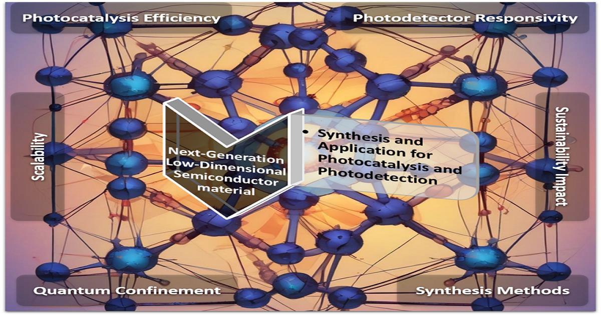
Next-Generation Low-Dimensional Semiconductor Materials: Synthesis and Applications for Photocatalysis and Photodetection
This special issue belongs to the section “Electronic Materials“.
Special Issue Information
Dear Colleagues,
Low-dimensional semiconductors (0D, 1D, 2D) exhibit quantum confinement effects and tunable optoelectronic properties, enabling breakthroughs in energy conversion, environmental remediation, and high-sensitivity photodetection. This Special Issue seeks to advance the synthesis, characterization, and application of low-dimensional semiconductors, emphasizing scalable fabrication, stability enhancement, and device integration for sustainable energy and sensing technologies.
Research History
- Post-2020: Integration of 2D materials (MoS2, MXenes) and stimuli-responsive systems for adaptive optoelectronics.
- 2010s–2020s: Emergence of hybrid materials (e.g., plasmonic–semiconductor nanostructures) and organic–inorganic perovskites, improving responsivity and catalytic efficiency.
- 2000s–2010s: Focus on inorganic nanowires (e.g., ZnO, CdS) and graphene for UV photodetectors and photocatalytic water splitting.
Latest Research Progress
- Plasmonic Hybrids: Enhanced light–matter interaction in Au/ZnO and graphene/MoS2 heterostructures for ultrasensitive photodetection and SERS-based biosensing.
- Perovskite Nanocrystals: CsCu2I3 and Cs3Cu2I5 demonstrate high photoluminescence quantum yield (PLQY >80%) for photocatalytic CO2 reduction.
- Flexible Organic Crystals: Low-dimensional organic semiconductors (e.g., S-BF2 nanowires) enable wearable UV photodetectors and optically pumped lasers 1013.
- 2D Ferroelectrics: Materials like 1T′-MoS2 show room-temperature ferroelectricity, which is promising for non-volatile memory and energy-efficient photodetectors.
We invite contributions addressing, but not limited to, the following:
- Synthesis: Novel methods (CVD, solution-phase epitaxy) for low-dimensional materials (quantum dots, nanowires, 2D perovskites).
- Characterization: Advanced techniques (in situ TEM, low-wave Raman spectroscopy) to probe atomic-scale structure–property relationships.
- Applications: Photocatalysis (H2 generation, pollutant degradation), photodetectors (UV-IR range), and integrated systems (e.g., perovskite/organic tandems).
We welcome the following:
- Original Research: Innovations in material design (e.g., defect engineering, phase-selective synthesis).
- Reviews: Critical analyses of challenges in scalability, stability, and interfacial charge transfer.
- Device Studies: Photodetectors with ultrahigh responsivity (>10⁴ A/W) or photocatalysts with >90% quantum efficiency.
- Theoretical Work: Computational modeling of exciton dynamics, carrier mobility, and heterostructure interfaces.
Prof. Dr. Lijun Wu
Dr. Jagadeesh Suriyaprakash
Dr. Lianwei Shan
Guest Editors
Manuscript Submission Information
Manuscripts should be submitted online at www.mdpi.com by registering and logging in to this website. Once you are registered, click here to go to the submission form. Manuscripts can be submitted until the deadline. All submissions that pass pre-check are peer-reviewed. Accepted papers will be published continuously in the journal (as soon as accepted) and will be listed together on the special issue website. Research articles, review articles as well as short communications are invited. For planned papers, a title and short abstract (about 250 words) can be sent to the Editorial Office for assessment.
Submitted manuscripts should not have been published previously, nor be under consideration for publication elsewhere (except conference proceedings papers). All manuscripts are thoroughly refereed through a single-blind peer-review process. A guide for authors and other relevant information for submission of manuscripts is available on the Instructions for Authors page. Materials is an international peer-reviewed open access semimonthly journal published by MDPI.
Please visit the Instructions for Authors page before submitting a manuscript. The Article Processing Charge (APC) for publication in this open access journal is 2600 CHF (Swiss Francs). Submitted papers should be well formatted and use good English. Authors may use MDPI's English editing service prior to publication or during author revisions.
Keywords
- low-dimensional semiconductors
- quantum-confined nanomaterials
- plasmonic–semiconductor hybrids
- photocatalytic CO2 reduction
- ultrahigh-responsivity photodetectors
- 2D perovskites
- solution-phase epitaxy
- exciton dynamics
- flexible optoelectronics
- defect engineering in nanostructures
Benefits of Publishing in a Special Issue
- Ease of navigation: Grouping papers by topic helps scholars navigate broad scope journals more efficiently.
- Greater discoverability: Special Issues support the reach and impact of scientific research. Articles in Special Issues are more discoverable and cited more frequently.
- Expansion of research network: Special Issues facilitate connections among authors, fostering scientific collaborations.
- External promotion: Articles in Special Issues are often promoted through the journal's social media, increasing their visibility.
- e-Book format: Special Issues with more than 10 articles can be published as dedicated e-books, ensuring wide and rapid dissemination.
Published Papers
Get Alerted
Add your email address to receive forthcoming issues of this journal.