
- 3.2Impact Factor
- 6.4CiteScore
- 16 daysTime to First Decision
Advanced Electroceramics and Their Applications in Energy Harvesting, Conversion and Storage
This special issue belongs to the section “Advanced and Functional Ceramics and Glasses“.
Special Issue Information
Dear Colleagues,
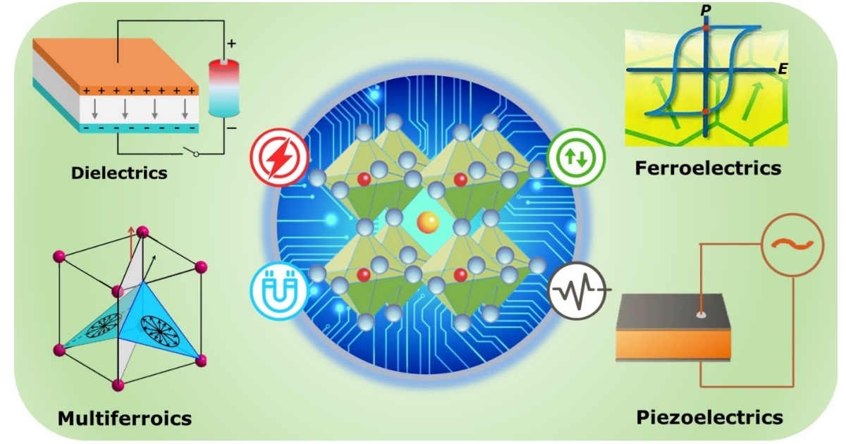
The need for research on sustainable and efficient energy solutions has never been more pressing than today. Electroceramics, with their unique properties and versatile applications, have emerged as promising candidates in this endeavor. Examples include dielectric, piezoelectric, ferroelectric, and multiferroic materials, which exhibit remarkable capacitive, electromechanical, and magnetoelectric properties. In particular, ferro-/piezoelectric materials can efficiently convert mechanical energy into electrical energy and vice versa, making them ideal for energy harvesting and conversion applications. Multiferroic materials enable efficient energy conversion between magnetic and electrical energy due to the bidirectional coupling between magnetic and electric properties. Additionally, the ability to store and release electrical energy in dielectric materials makes them useful for energy storage devices. Intensive research has been carried out around the world to develop novel electroceramic materials, fabrication techniques, and device architectures to enhance energy density, efficiency, durability, and reliability, leading to significant progress in recent years. This Special Issue aims to showcase the latest advancements in this field, providing a platform for researchers to share their new insights, innovative methodologies, and latest findings. We welcome research papers or review articles that explore and discuss various aspects of advanced electroceramics, including but not limited to:
- Novel synthesis and fabrication techniques for advanced electroceramics;
- Structural characterization of advanced electroceramics;
- Physical and chemical properties of advanced electroceramics;
- Modelling and simulation of electroceramic materials and devices;
- Applications of electroceramics in energy harvesting, conversion, and storage technologies.
Dr. Zenghui Liu
Dr. Pan Gao
Prof. Dr. Zuo-Guang Ye
Guest Editors
Manuscript Submission Information
Manuscripts should be submitted online at www.mdpi.com by registering and logging in to this website. Once you are registered, click here to go to the submission form. Manuscripts can be submitted until the deadline. All submissions that pass pre-check are peer-reviewed. Accepted papers will be published continuously in the journal (as soon as accepted) and will be listed together on the special issue website. Research articles, review articles as well as short communications are invited. For planned papers, a title and short abstract (about 250 words) can be sent to the Editorial Office for assessment.
Submitted manuscripts should not have been published previously, nor be under consideration for publication elsewhere (except conference proceedings papers). All manuscripts are thoroughly refereed through a single-blind peer-review process. A guide for authors and other relevant information for submission of manuscripts is available on the Instructions for Authors page. Materials is an international peer-reviewed open access semimonthly journal published by MDPI.
Please visit the Instructions for Authors page before submitting a manuscript. The Article Processing Charge (APC) for publication in this open access journal is 2600 CHF (Swiss Francs). Submitted papers should be well formatted and use good English. Authors may use MDPI's English editing service prior to publication or during author revisions.
Keywords
- electroceramics
- dielectric materials
- piezoelectric materials
- ferroelectric materials
- multiferroic materials
- energy storage
- energy conversion
- energy harvesting
Benefits of Publishing in a Special Issue
- Ease of navigation: Grouping papers by topic helps scholars navigate broad scope journals more efficiently.
- Greater discoverability: Special Issues support the reach and impact of scientific research. Articles in Special Issues are more discoverable and cited more frequently.
- Expansion of research network: Special Issues facilitate connections among authors, fostering scientific collaborations.
- External promotion: Articles in Special Issues are often promoted through the journal's social media, increasing their visibility.
- e-Book format: Special Issues with more than 10 articles can be published as dedicated e-books, ensuring wide and rapid dissemination.
Published Papers
Get Alerted
Add your email address to receive forthcoming issues of this journal.