


Abstract
Flexible wearable biosensors have emerged as a promising technology for continuous, noninvasive health monitoring, driven by the growing demand for personalized healthcare and an aging global population. Polymeric substrates such as polyethylene terephthalate (PET), polyimide (PI), and polydimethylsiloxane (PDMS) provide lightweight, flexible, and low-cost platforms that conform to the human body, but their practical deployment requires reliable integration with complementary metal–oxide–semiconductor (CMOS) electronics for signal acquisition, processing, and wireless communication. This review summarizes recent advances in CMOS-compatible flexible biosensors, emphasizing polymer-based sensing platforms, circuit-level integration, and system-on-chip (SoC) architectures for wearable healthcare applications. Flexible sensing mechanisms, including electrochemical, capacitive, resistive, and transistor-based devices, are discussed alongside CMOS analog front-end circuits, low-noise amplifiers, analog-to-digital converters, and ultra-low-power signal conditioning techniques. Finally, key challenges in CMOS–flexible sensor integration, including mechanical reliability, biocompatibility, signal integrity, packaging, and scalable manufacturing, are discussed, together with future directions toward highly integrated, intelligent, and energy-efficient wearable healthcare systems.
1. Introduction
Healthcare is experiencing a conceptual shift from reactive, hospital-centered treatment to proactive, personalized, and continuous care. This transformation is being driven by several converging global challenges. First, the world’s aging population is increasing the prevalence of chronic diseases such as cardiovascular disorders, diabetes, and neurodegenerative conditions, placing unprecedented demands on healthcare systems [1]. Second, escalating healthcare costs have highlighted the need for affordable technologies that enable early disease detection, remote patient monitoring, and preventive interventions outside traditional clinical settings [2]. At the same time, the emergence of personalized medicine has created demand for physiological monitoring tailored to individual patients rather than periodic, population-based assessments.
Wearable biosensors have emerged as a key enabling technology to address these challenges by providing continuous, noninvasive measurement of physiological and biochemical biomarkers in real-world environments [3,4]. Unlike conventional diagnostic methods that rely on intermittent clinical visits, wearable sensing platforms enable real-time monitoring of health status, allowing earlier detection of abnormalities and more timely clinical decision-making.
The evolution of wearable biomedical devices has been marked by a significant transition from conventional rigid silicon-based electronics to flexible, lightweight, and skin-conformal sensing [5]. Traditional silicon electronics have long served as the foundation of medical instrumentation due to their excellent electrical performance, high integration density, and mature CMOS fabrication processes. However, their inherent rigidity and brittleness limit their compatibility with soft, curved, and dynamically moving biological tissues. Conventional devices often require bulky packaging and rigid interconnects, making them unsuitable for long-term, continuous monitoring where user comfort and mechanical compliance are essential. Consequently, the need for wearable systems capable of operating reliably under repeated bending, stretching, and deformation has motivated the development of flexible electronic technologies.
Recent advances in flexible electronics have enabled the fabrication of high-performance sensors on polymer substrates such as polyethylene terephthalate (PET), polyimide (PI), and polydimethylsiloxane (PDMS). These materials offer excellent mechanical flexibility, low weight, optical transparency, and biocompatibility while remaining compatible with a wide range of printing and microfabrication techniques. Flexible devices can conform to irregular surfaces without significantly compromising electrical performance, enabling continuous monitoring of physiological signals during everyday activities. Building upon these developments, skin-conformal electronic systems have emerged as a new generation of wearable platforms that intimately laminate onto the epidermis, creating stable mechanical and electrical interfaces with minimal discomfort. Often referred to as electronic skin (e-skin), these systems enable high-fidelity acquisition of electrophysiological, mechanical, and biochemical signals by minimizing motion artifacts and improving sensor-to-skin contact [6,7].
However, realizing this vision requires more than advances in sensing materials alone. High-performance wearable systems depend on seamless integration between flexible sensing platforms and complementary metal–oxide–semiconductor (CMOS) electronics. The electrical signals generated by wearable biosensors are often extremely weak, susceptible to environmental noise, and require substantial processing before meaningful physiological information can be extracted. When integrated with ultra-low-power CMOS readout circuits, wireless communication modules, and embedded signal processing, skin-conformal biosensors provide a promising foundation for next-generation personalized healthcare, remote patient monitoring, and point-of-care diagnostics.
The analog front-end (AFE) forms the interface between the flexible sensor and the digital processing chain. It typically comprises low-noise amplifiers, instrumentation amplifiers, transimpedance amplifiers, filters, and analog-to-digital converters (ADCs) that amplify weak sensor outputs, suppress interference, and prepare signals for digital processing. Because physiological and electrochemical signals often have amplitudes in the microvolt to millivolt range, effective signal conditioning is essential to minimize motion artifacts, electromagnetic interference, and baseline drift.
Ultra-low power operation is equally critical for wearable healthcare systems. CMOS circuits employ low-voltage design, efficient power management, and wireless communication technologies such as Bluetooth Low Energy (BLE), Near-field communication (NFC), and Ultra-WideBand (UWB) to maximize battery lifetime while enabling continuous data transmission. More recently, embedded microcontrollers and Edge AI accelerators have enabled on-device feature extraction, anomaly detection, and activity recognition, reducing communication bandwidth, improving privacy, and supporting intelligent, energy-efficient wearable healthcare systems [8,9].
This review provides a comprehensive overview of CMOS-compatible flexible biosensors fabricated on polymer substrates, with particular emphasis on PET, PI, PDMS, and related soft polymer materials for wearable healthcare applications. Unlike reviews that treat materials, circuits, and system integration separately, the primary objective is to bridge three complementary research domains that are often treated independently: flexible polymer-based sensing technologies, CMOS integrated circuits for signal acquisition and processing, and system-level wearable electronic platforms. Rather than focusing solely on sensing materials or electronic interfaces, this review examines how these technologies can be co-designed and integrated to realize compact, low-power, and high-performance wearable biosensing systems.
The discussion encompasses flexible electrochemical, capacitive, resistive, and transistor-based biosensors. Integration strategies are also reviewed with emphasis on their suitability for large-scale manufacturing and long-term wearable operation.
This review does not focus on nanomaterial synthesis or growth as a primary topic. Laser-induced graphene (LIG) is discussed as a limited exception because it is formed by direct laser conversion of an existing polymer substrate rather than by separate nanomaterial synthesis or transfer, and it is included only where the resulting device illustrates flexible-system integration or CMOS-relevant readout considerations. Nanomaterial-containing devices are included only when they illustrate system-level CMOS integration, flexible packaging, or readout-circuit design. Although these materials have demonstrated exceptional sensing performance, their reliable, scalable, and CMOS-compatible integration remains an active area of research and has not yet reached the level of maturity required for widespread commercial wearable systems. Likewise, optical sensing technologies, including fluorescence and spectroscopic biosensors, are beyond the scope of this review, which focuses exclusively on electrically transduced biosensors and their integration with CMOS electronics. By concentrating on polymer-based electrical sensors and CMOS-compatible system architectures, this review aims to provide a focused perspective on technologies that are closest to practical implementation in next-generation wearable healthcare devices.
2. Polymer Platforms and CMOS Integration Constraints for Flexible Biosensors
Flexible biosensing systems require mechanically compliant substrates that support sensing layers, interconnects, encapsulation, and electrical interfaces to rigid or thinned CMOS integrated circuits. Polymer substrates are therefore not merely mechanical carriers; their thermal, chemical, dielectric, and mechanical properties directly constrain sensor fabrication, chip attachment, interconnect formation, and system packaging. In most practical implementations, the sensing surface and interconnect network are fabricated on a thin polymer substrate, whereas signal conditioning and data processing are performed by a rigid, thinned, or mechanically isolated CMOS die. The compliant portion of the system can conform to curved and moving body surfaces, improving sensor–skin contact, reducing motion-induced disturbances, and enhancing comfort during extended use [10]. Compared with bulk silicon substrates, thin polymer films tolerate substantially greater bending deformation; however, system reliability is often limited by the deposited conductors, chip-to-substrate interconnects, solder joints, and material interfaces rather than by the polymer alone.
Selected polymer substrates are low-cost and compatible with scalable patterning methods such as screen, inkjet, aerosol-jet, and roll-to-roll processing [11]. Their suitability for biomedical use nevertheless depends on material grade, surface chemistry, residual solvents, deposited layers, adhesives, and encapsulation. Because conventional CMOS fabrication cannot normally be performed directly on low-temperature polymer substrates, flexible biosensors generally employ heterogeneous integration through flip-chip attachment, wire bonding, anisotropic conductive adhesives, flexible printed circuits, or transfer printing [12,13,14]. Substrate selection determines not only mechanical conformity but also the thermal budget, lithographic resolution, interconnect reliability, dielectric behavior, moisture stability, and packaging options of the complete sensing system. Relevant parameters include elastic modulus, coefficient of thermal expansion, glass-transition temperature, surface roughness, solvent resistance, water-vapor permeability, dielectric properties, and compatibility with metallization and chip-attachment processes. In this review, “CMOS compatibility” refers primarily to heterogeneous assembly, packaging, transfer, or low-temperature post-processing after CMOS fabrication, rather than conventional front-end CMOS processing performed directly on a polymer substrate [13,14].
2.1. Polymer Substrates: Properties and Chip-Integration Implications
The polymer substrates most frequently used in flexible and wearable electronics differ substantially in thermal budget, stiffness, dimensional stability, surface chemistry, and compatibility with chip packaging. These differences determine whether a material is best used as a sensor substrate, flexible interposer, stretchable carrier, microfluidic layer, or encapsulant.
Polyethylene Terephthalate (PET) is widely used for low-cost flexible sensors because it is transparent, lightweight, commercially available in large-area films, and compatible with printing and roll-to-roll manufacturing. Its principal limitation is its relatively low thermal budget: practical processing temperatures are commonly kept below approximately 120–150 °C, although short process excursions may be possible depending on the PET grade and mechanical constraint [15]. Consequently, PET is most suitable for printed conductors, low-temperature sensing layers, and hybrid attachment of separately fabricated CMOS dies rather than direct high-temperature semiconductor processing. PET’s coefficient of thermal expansion and dimensional change during heating can reduce fine-pitch chip-alignment accuracy.
Polyimide (PI) is commonly used in high-performance flexible circuits because selected formulations provide high thermal stability, chemical resistance, and mechanical durability. Depending on the formulation and cure history, selected PI films can tolerate processing temperatures above 300 °C, allowing a wider range of metallization, dielectric and packaging processes than PET [13,16]. PI is therefore widely used in flexible printed circuits, redistribution layers, chip-scale interposers, and substrates that carry thinned or flip-chip-mounted CMOS dies. Its limitations include moisture uptake, relatively high stiffness compared with elastomers, and the reduced optical transparency of conventional amber PI.
Polydimethylsiloxane (PDMS) is a silicone elastomer used in epidermal devices, stretchable sensors, and microfluidic structures because of its low elastic modulus, optical transparency, and ability to accommodate large strain. However, its low surface energy complicates metallization and adhesive bonding, while solvent-induced swelling, permeability to gasses and water vapor, and dimensional instability can affect fabrication and long-term operation [13,17]. Rigid CMOS dies mounted on PDMS, therefore, require local mechanical islands, strain-isolation structures, compliant interconnects, or an intermediate flexible circuit.
Ecoflex is a commercial silicone elastomer used when very low modulus and high stretchability are required. Depending on the grade and curing conditions, it can sustain strains of several hundred percent and reduce mechanical loading at skin-mounted interfaces [18]. However, its softness makes fine-pattern alignment, direct metallization, and chip attachment difficult. Ecoflex is therefore generally used as a compliant carrier, encapsulant, or strain-isolation layer rather than as a substrate for high-density CMOS interconnects.
Thermoplastic PolyUrethane (TPU) is a family of elastic thermoplastics used in wearable patches, textiles, cable-like interconnects, and protective laminates. TPU provides useful abrasion resistance and can be processed by lamination, extrusion, printing, and additive manufacturing; however, its thermal behavior, moisture absorption, modulus, and chemical resistance vary substantially among grades [14]. In CMOS-integrated wearable, TPU is most often used as a compliant carrier or encapsulation layer, while high-density chip interconnection is implemented on a more dimensionally stable flexible circuit.
Parylene-C is deposited by room-temperature chemical vapor deposition and forms thin, conformal dielectric films over sensors, interconnects, and CMOS components. It is used as an encapsulant and, in some microsystems, as a free-standing flexible substrate. Its electrical insulation, chemical resistance, and established use in biomedical devices are advantageous, although moisture protection depends on film thickness, defect density, adhesion, and the integrity of edges and feedthroughs [19].
PolyEthylene Naphthalate (PEN) occupies an intermediate processing range between PET and high-temperature PI. Relative to typical PET films, PEN generally provides improved dimensional and thermal stability and reduced moisture uptake while retaining optical transparency [12]. It can therefore support finer printed features and moderately higher-temperature processing, although its thermal budget remains below that of many PI formulations. PEN is primarily suited to printed sensor platforms and hybrid CMOS assembly rather than direct semiconductor fabrication.
No single substrate optimizes stretchability, dimensional stability, thermal budget, dielectric performance, biocompatibility, and chip-packaging compatibility simultaneously. PET and PEN favor low-cost, large-area manufacturing; PI supports higher-temperature processing and denser flexible interconnects; PDMS and Ecoflex provide stretchability but complicate fine-pitch assembly; TPU is useful for mechanically durable wearable structures; and Parylene-C is particularly valuable for conformal dielectric and encapsulation layers. Material selection therefore depends on the architecture of the complete sensor–interconnect–CMOS–package stack rather than on the properties of the polymer in isolation. Table 1 compares the principal integration-relevant characteristics of these materials.
Table 1.
Comparison of polymer materials used in flexible biosensors and their implications for heterogeneous CMOS integration. The reported temperatures correspond to typical processing temperatures rather than polymer decomposition temperatures and may vary depending on material grade and fabrication process.
Polymer backbone chemistry influences chain rigidity, glass-transition behavior, solvent resistance, moisture uptake, dielectric properties, and adhesion to deposited metals and dielectrics. These factors affect lithographic alignment, residual stress, interconnect reliability, and encapsulation performance in hybrid CMOS systems. Figure 1 relates representative polymer structures to their principal system-level functions. Aromatic backbones in PET, PI, and PEN generally increase chain rigidity and dimensional stability, although the resulting thermal and mechanical properties remain formulation dependent. Silicone elastomers such as PDMS contain flexible siloxane backbones that produce low modulus and high deformability but also create challenges in adhesion and fine-pattern fabrication. TPU contains alternating hard and soft segments whose composition controls elasticity and thermal behavior. Parylene-C forms a conformal dielectric film through vapor-phase polymerization and is therefore particularly useful for electrical insulation and environmental protection. These structure–property relationships remain qualitative because processing history, molecular weight, additives, film thickness, and curing conditions strongly affect the final properties.
Figure 1.
Comparison of representative polymer substrates for CMOS-compatible flexible biosensors. The figure summarizes the chemical repeat units, optical transparency, mechanical flexibility, processing temperature, CMOS compatibility, and typical applications of PET, PI, PDMS, TPU, Parylene-C, and PEN. Star ratings provide a qualitative comparison of key material (five stars = excellent; one star = poor). Ecoflex is excluded because it is a cross-linked elastomer rather than a polymer with a well-defined repeat unit.
2.2. Fabrication and Heterogeneous CMOS Integration Technologies
The fabrication of a CMOS-integrated flexible biosensor usually comprises two distinct process streams: low-temperature formation of the flexible sensor and interconnect layers, and conventional wafer-based fabrication of the CMOS die. These streams are subsequently combined through heterogeneous assembly. Polymer processing must remain below the thermal and chemical limits of the substrate, whereas chip attachment must provide low-resistance electrical connections without introducing excessive local stress. Accordingly, fabrication-method selection affects feature size, alignment accuracy, material compatibility, throughput, interconnect parasitics, mechanical reliability, and production cost (Figure 2) [20].
Figure 2.
Representative process flows for fabricating flexible sensing layers and integrating them with CMOS electronics. Printing, roll-to-roll processing, laser patterning, and polymer-compatible photolithography primarily form sensors and interconnects, whereas transfer printing and chip-attachment methods combine separately fabricated CMOS devices with flexible substrates. Process selection depends on feature size, substrate thermal budget, alignment tolerance, production throughput, and package-reliability requirements.
Inkjet printing is a maskless, digitally patterned deposition method used for conductive traces, dielectric layers, functional coatings, and selected biorecognition materials. On PET, PEN, PI, and TPU, practical feature dimensions are commonly in the tens-of-micrometers range and depend on drop volume, ink rheology, surface energy, substrate treatment, and drop spacing. Conductive nanoparticle inks generally require thermal, photonic, or chemical sintering, and the substrate thermal budget limits the applicable sintering conditions. Inkjet printing is therefore well suited to sensor electrodes and low-density interconnects but is less suitable than lithographic methods for fine-pitch CMOS input/output redistribution.
Screen printing provides high-throughput deposition of relatively thick conductive and sensing layers over large areas. Silver, carbon, conductive-polymer, and composite inks can be patterned to form electrodes and interconnects for disposable electrochemical sensors. Its principal advantages are low cost and manufacturing maturity, whereas its limitations include relatively coarse feature size, layer-to-layer registration error, surface roughness, and variability in printed thickness. These limitations generally restrict screen-printed conductors to sensor-level routing rather than direct fine-pitch connection to a CMOS die [20].
Aerosol jet printing uses an aerodynamically focused aerosol stream to deposit conductive and dielectric materials on planar or non-planar surfaces. Feature widths below approximately 20 m have been reported under optimized conditions, although electrical performance and manufacturing yield depend strongly on ink formulation, overspray, nozzle condition, curing, and substrate topography. The technique is attractive for flexible hybrid electronics because it can print local interconnects between chip pads and flexible traces; however, connection resistance, adhesion, encapsulation, and cyclic-bending reliability remain specific to each material stack [20].
Roll-to-roll (R2R) processing is a manufacturing framework rather than a single patterning technique. It combines web handling with printing, coating, drying, curing, registration, lamination, and encapsulation. The method is attractive for high-volume sensor films and disposable patches on PET or PEN, but the integration of discrete CMOS dies remains challenging because chip placement, fine-pitch alignment, web deformation, and local packaging interrupt the otherwise continuous process [21]. Consequently, practical manufacturing may combine roll-to-roll sensor fabrication with a subsequent sheet-based or pick-and-place chip-assembly step.
Laser patterning can define metal traces, remove selected material, modify polymer surfaces, and form microfluidic structures without a physical mask. Local energy deposition can create a heat-affected zone and distort the substrate. Laser-induced carbonization of suitable polymers can also form conductive porous sensing structures, but this direct polymer-conversion process is distinct from the graphene or nanomaterial-growth technologies excluded from the main scope of this review. Laser processing is particularly useful for rapid prototyping and local pattern modification, but uniformity, debris generation, and large-area throughput remain important considerations.
Transfer printing enables separately fabricated silicon devices, thin-film components, or micro-LEDs to be released from a donor wafer and positioned on a polymer receiver substrate. For flexible biosensors, the method can reduce the effective thickness and bending stiffness of the silicon component while preserving CMOS-level device performance. Its key technical challenges include release yield, placement accuracy, interfacial adhesion, electrical interconnection, and protection of the transferred die during repeated deformation. Transfer printing is therefore a heterogeneous integration method rather than a substitute for conventional CMOS fabrication.
Photolithography remains necessary when the flexible platform requires micrometer-scale electrodes, thin-film transistors, dense redistribution lines, or precise alignment. Polymer-compatible photolithography may use low-temperature resists, lift-off, wet or dry etching, and temporary carrier wafers. Among the techniques summarized here, photolithography generally provides the finest feature resolution, but it increases process complexity and cost and may expose the polymer to solvents, plasma treatments, elevated temperatures, and thermomechanical stress [13,20]. Photolithography on a polymer substrate is a back-end patterning step and is distinct from the front-end lithographic processes used to fabricate the CMOS die.
After sensor fabrication, the flexible substrate and CMOS die are joined electrically and mechanically. Common approaches include wire bonding, flip-chip bonding, anisotropic conductive films or pastes, conductive adhesives, solder attachment on flexible printed circuits, and printed interconnect bridging. The selected method determines pad pitch, contact resistance, parasitic capacitance, package thickness, fatigue behavior, and compatibility with encapsulation. For highly deformable systems, the CMOS die is commonly positioned on a locally stiffened island and connected to the sensing region through serpentine or otherwise strain-relieved conductors [10,12,14].
Fabrication-method selection depends on the required sensor resolution and production volume together with the interconnection requirements of the CMOS interface. Screen and roll-to-roll printing favor low-cost, high-volume sensor production; inkjet and aerosol-jet printing provide digital patterning and rapid design modification; laser processing supports local, maskless structuring; and photolithography enables dense, high-resolution features. No single technique spans both large-area disposable sensing layers and fine-pitch chip interconnection. Hybrid process flows therefore combine scalable printed sensor fabrication with localized lithography, flexible-circuit redistribution, or chip-level assembly. Table 2 compares these techniques while distinguishing sensor fabrication from CMOS-die integration.
Table 2.
Comparison of fabrication and assembly technologies for polymer-based sensors and heterogeneous CMOS integration.
3. Flexible Biosensing Mechanisms
Cross-study comparison depends on four coupled factors: the biological or physical variable being measured, the signal range and noise environment at the CMOS input, the validation setting, and the sources of irreproducibility or barriers to clinical transfer. Reported sensitivity or resolution alone cannot rank devices because electrochemical measurements, mechanical transduction, physiological recording, and environmental monitoring operate at different bandwidths and under different calibration and packaging constraints. The evidentiary assessment therefore combines performance with sample size, test duration, calibration procedure, drift, interference rejection, cross-device variability, and the distinction between benchtop and on-body validation. This section reviews electrochemical, mechanical, physiological, and environmental sensing platforms and their corresponding CMOS interfaces. Although the sensing elements and analog front-end circuits differ according to the measured quantity, the system architecture becomes largely common after analog-to-digital conversion. As summarized in Figure 3, the digitized data are managed by digital control logic, transmitted through a low-power wireless interface, and supported by an integrated power-management subsystem.
Figure 3.
Common CMOS back-end architecture used after signal digitization in flexible electrochemical, mechanical, and environmental sensing systems. The analog-to-digital converter output is processed by digital control logic responsible for clock generation, sensor multiplexing, calibration, drift compensation, and data formatting. A wireless communication module provides low-power data transmission, typically through BLE, while the power-management unit regulates the battery or harvested energy using DC–DC converters and low-dropout regulators.
The digital control block provides clock generation, sensor multiplexing, calibration, drift compensation, and data formatting before transmission. Wireless communication is commonly implemented using an RF transmitter and BLE, while the power-management unit supplies regulated voltages through battery, DC–DC converter, and low-dropout regulator interfaces. These blocks are repeated across the electrochemical, mechanical, and environmental sensing systems discussed in the following subsections because they form a shared CMOS back-end architecture.
3.1. Electrochemical Sensors
Electrochemical sensing has become one of the most widely adopted approaches for flexible wearable biosensors because of its high sensitivity, low power consumption, ease of miniaturization, and compatibility with CMOS readout circuits. Unlike optical sensing techniques, electrochemical sensors directly convert chemical reactions into measurable electrical quantities, enabling compact and energy-efficient detection of a wide variety of physiological biomarkers. Most flexible electrochemical sensors employ either two- or three-electrode configurations consisting of working, reference, and counter electrodes fabricated on polymer substrates such as PET, PI, PDMS, or FPCBs. These sensing platforms can be readily integrated with CMOS analog front-end circuits for current measurement, voltage regulation, digitization, and wireless communication, making them attractive for continuous health monitoring applications [22,23].
Electrochemical sensing enables continuous monitoring of numerous physiological biomarkers in noninvasive biofluids [24]. Electrolytes such as sodium and potassium are commonly measured using potentiometric ion-selective electrodes for hydration assessment and sweat analysis, whereas pH sensing provides valuable information regarding gastrointestinal disorders, wound healing, and metabolic conditions [25,26]. Glucose and lactate are typically monitored using amperometric enzymatic biosensors [22] for diabetes management and exercise physiology, while voltammetric techniques support multiplexed biochemical analysis and cellular monitoring. Impedance spectroscopy [27,28] enables label-free assessment of tissue growth, wound healing, and implant health. Together, these electrochemical sensing modalities provide a versatile platform that can be efficiently integrated with flexible polymer electronics and CMOS readout circuits for next-generation wearable healthcare systems.
Figure 4 illustrates the typical architecture of a CMOS-compatible flexible electrochemical biosensing platform. The sensing interface consists of a conventional three-electrode configuration composed of the working electrode (WE), reference electrode (RE), and counter electrode (CE), which enables potentiometric, amperometric, and voltammetric measurements. The electrochemical response generated by the sensor is first processed by a CMOS AFE, which typically incorporates a potentiostat to regulate the electrode potentials, a chopper-stabilized amplifier for low-noise operation, and a current-to-voltage conversion stage for accurate measurement of the sensor current. The conditioned analog signal is subsequently digitized using an ultra-low-power ADC, such as a successive approximation register (SAR), sigma–delta, or time-based VCO architecture.
Figure 4.
Typical architecture of a CMOS-compatible flexible electrochemical biosensing platform.
3.1.1. Potentiometric Sensors
Potentiometric sensors measure the equilibrium potential difference between an ion-selective working electrode and a stable reference electrode under negligible current flow. The measured voltage follows the Nernst relationship and is proportional to the logarithm of the target ion concentration. This sensing principle is widely employed for electrolyte monitoring because it provides high sensitivity while consuming extremely little power.
A representative example is the fully flexible sodium ion-selective electrode (SS-ISE) developed by Lim et al., where an Au/CNT/Au nanocomposite transducer was integrated with flexible thin-film electronics to realize a wireless, skin-mounted sodium monitoring platform. The device demonstrated a near-Nernstian sensitivity of 55.5 ± 0.3 mV/decade while maintaining less than 3% variation during continuous body motion, illustrating the potential of flexible potentiometric sensors for long-term electrolyte monitoring [23]. Another example is the self-orienting ingestible capsule reported by Abdigazy et al., which integrates a miniature three-electrode pH sensor with a custom CMOS chip fabricated in a 180-nm process. The chip incorporates a chopper-stabilized analog front-end, a low-power time-based ADC, an RF transmitter operating in the Medical Implant Communication System (MICS) band, and an integrated power management unit. Mounted on a flexible polyimide printed circuit board, the system demonstrates the advantages of combining electrochemical sensing with monolithic CMOS integration for continuous gastrointestinal pH monitoring [22].
3.1.2. Amperometric Sensors
Amperometric sensors determine analyte concentration by measuring the oxidation or reduction current generated at a constant electrode potential. Since the measured current is directly proportional to the electrochemical reaction rate, amperometric sensing provides excellent sensitivity and is widely employed for enzymatic biosensors. A representative example is the ultra-thin chitosan–graphene oxide (CS–GO) biosensor developed by Kafi et al. for diabetic wound monitoring. The flexible sensor patch combines gold microelectrodes with a CS–GO substrate and demonstrates glucose detection over concentrations ranging from 1 M to 20 mM while simultaneously monitoring cell proliferation. The work illustrates the suitability of flexible amperometric biosensors for continuous biochemical monitoring in wound-care applications [29].
The ingestible CMOS platform developed by Abdigazy et al. also supports amperometric measurements through a bidirectional three-electrode potentiostat capable of measuring oxidation and reduction currents over a A range with a minimum detectable current of 150 pA while consuming approximately 1 W, demonstrating the effectiveness of ultra-low-power CMOS analog front ends for electrochemical sensing [22].
3.1.3. Voltammetric Sensors
Voltammetric sensors measure the current response while sweeping the electrode potential according to a predefined excitation waveform. Unlike amperometric sensing, voltammetry provides additional electrochemical information, including oxidation and reduction peak potentials, enabling characterization of reaction kinetics and simultaneous detection of multiple analytes.
The CS–GO wound monitoring platform developed by Kafi et al. employs cyclic voltammetry to monitor human dermal fibroblast proliferation. Stable anodic and cathodic peaks were maintained over repeated scan cycles, while the peak current increased with cell proliferation and glucose concentration, demonstrating the capability of flexible voltammetric sensors for simultaneous biochemical sensing and tissue monitoring [29]. Such systems can be readily interfaced with programmable CMOS potentiostats capable of generating excitation waveforms while accurately measuring the resulting electrochemical currents.
3.1.4. Impedance Sensors
Electrochemical impedance spectroscopy (EIS) characterizes the complex impedance of biological tissues or electrochemical interfaces over a range of excitation frequencies. Rather than measuring a single current or voltage, impedance sensing evaluates both resistive and capacitive components, providing information regarding cellular attachment, tissue growth, interface degradation, and electrode condition.
Marland et al. developed a flip-chip-on-flex impedance spectroscopy sensor for synthetic vascular graft monitoring using an array of interdigitated platinum electrodes fabricated on a silicon die and integrated onto a flexible substrate through flip-chip-on-flex packaging. The miniature sensor successfully detected vascular smooth muscle cell growth through impedance changes while demonstrating the feasibility of combining CMOS-compatible microfabrication with flexible packaging for implantable biosensing applications [28].
Across electrochemical modalities, the principal trade-off is between chemical selectivity, electrode stability, circuit complexity, and power. Potentiometric interfaces can operate with very small currents and therefore favor low-power voltage readout, but their accuracy depends on reference-electrode stability, ionic strength, temperature, and calibration drift. Amperometric and voltammetric systems provide richer reaction information and can support multi-analyte analysis, yet they require low-noise current-to-voltage conversion, bias control, and protection against electrode fouling. Impedance systems can monitor interfacial or cellular changes without labels, but their interpretation is frequency dependent and sensitive to parasitic capacitance, electrode geometry, and fixture conditions. The cited results are therefore strongest when they report calibration range, limit of detection, selectivity, repeatability, and storage or on-body duration together; many studies report only benchtop measurements with small numbers of devices, which limits claims about inter-laboratory reproducibility [28,30].
3.2. Mechanical Sensors
Mechanical sensors convert externally applied forces, pressure, strain, or deformation into measurable electrical signals and constitute one of the largest classes of flexible wearable sensors. Owing to their simple device structures, low manufacturing cost, and compatibility with flexible polymer substrates, mechanical sensors have found widespread applications in wearable healthcare, e-skin, human–machine interfaces, robotic manipulation, and physiological monitoring. Depending on the sensing mechanism, flexible mechanical sensors can generally be classified as capacitive, resistive, and piezoelectric sensors. Each sensing modality offers distinct advantages with respect to sensitivity, dynamic range, power consumption, and compatibility with CMOS readout electronics [31].
Figure 5 compares the typical CMOS-compatible system architectures employed for capacitive and resistive flexible mechanical sensors. While the sensing interfaces differ according to the transduction mechanism, both systems utilize similar CMOS building blocks. This common architecture enables scalable integration of large sensor arrays with low-power signal conditioning and wireless data transmission for wearable biomedical applications.
Figure 5.
Representative CMOS-compatible architectures for flexible mechanical sensing systems. Left: A capacitive sensing platform to accurately measure small capacitance variations produced by pressure, tactile, or proximity stimuli. Right: A resistive (piezoresistive) sensing platform employing a flexible resistive sensor array for real-time monitoring in wearable healthcare, electronic skin, and robotic sensing applications.
3.2.1. Capacitive Sensors
Capacitive sensors are widely used in flexible wearable electronics because of their high sensitivity, low power consumption, and compatibility with CMOS readout circuits [32,33]. Their operation is based on measuring capacitance variations caused by changes in electrode spacing, overlapping area, or dielectric properties under external pressure or deformation. Since the resulting capacitance changes are often in the femtofarad range, dedicated CMOS capacitance readout circuits, including switched-capacitor interfaces and capacitance-to-voltage converters, are required to achieve high sensitivity and low noise.
Peng and Lu demonstrated one of the earliest CMOS-integrated flexible capacitive sensor arrays using a tactile array fabricated on FPCBs with custom switched-capacitor readout circuits. The system achieved an average sensitivity of 1.57 mV/mmHg while resolving sub-femtofarad capacitance variations for real-time pulse diagnosis [32]. More recently, Tsao and Lu developed an flexible tactile and proximity sensor array integrated with CMOS readout circuitry, achieving a tactile sensitivity of 2.2 MPa−1, a pressure resolution of approximately 255 Pa, and a proximity sensing range of about 15 mm [33]. These studies demonstrate that CMOS-compatible capacitive sensors enable compact, low-power platforms for pressure monitoring, electronic skin, robotic manipulation, and human–machine interfaces.
3.2.2. Resistive (Piezoresistive) Sensors
Resistive sensors convert mechanical deformation into measurable resistance variations arising from changes in conductive pathways, contact resistance, or intrinsic piezoresistive effects. Compared with capacitive sensors, they require simpler readout circuitry, making them attractive for large-area pressure mapping, strain sensing, gait analysis, and wearable tactile sensing. Their compatibility with low-power CMOS electronics also enables highly integrated wearable sensing systems.
A representative example is the wearable gait monitoring system reported by Tian et al., in which a flexible piezoresistive pressure sensor array was integrated with an ultra-low-power near-sensor CMOS AI chip. The system achieved real-time gait recognition with an accuracy of 92% while consuming only 1.45 mW, demonstrating the benefits of combining flexible sensors with local CMOS processing [34]. Mahsereci et al. further demonstrated an ultra-thin flexible CMOS stress sensor in which the sensing elements, analog front end, SAR ADC, and digital controller were monolithically integrated within a 20 m-thick silicon die for robotic applications [35]. Han et al. also demonstrated multifunctional laser-induced graphene (LIG) sensors capable of electrochemical and strain sensing, illustrating the versatility of advanced conductive materials for future hybrid CMOS platforms [36]. More recently, flexible piezoelectric sensor arrays integrated with custom CMOS readout circuits have achieved 5 Pa pressure resolution, high-resolution tactile mapping, and low-power operation, extending wearable sensing to dynamic pressure monitoring and robotic applications [37,38].
The mechanical-sensor studies show a different validation pattern. Capacitive devices generally offer low static power and straightforward multiplexing, but parasitic capacitance, hysteresis, dielectric relaxation, and mechanical cross-talk can limit array-level accuracy. Resistive and piezoresistive devices are easier to interface with CMOS voltage or current readout, but they may exhibit larger baseline drift, temperature dependence, and cycle-to-cycle variation. Piezoelectric devices are attractive for dynamic pressure or vibration because they can generate a signal without continuous bias, whereas their response to static loads is intrinsically limited. Loading rate, force range, hysteresis, repeatability, spatial resolution, and cycle count therefore provide a more complete basis for comparison than sensitivity alone. Evidence obtained from isolated benchtop loading does not establish performance during skin motion, sweat exposure, or long-term attachment [31].
3.3. Physiological Sensors
Physiological sensors monitor the electrical and mechanical activity of the human body to provide continuous assessment of cardiovascular, neuromuscular, and respiratory health. Unlike electrochemical and mechanical sensors, they acquire weak endogenous bioelectrical signals, including ECG, EMG, EEG, and other electrophysiological signals. These biosignals typically range from a few microvolts to several millivolts with bandwidths below several hundred hertz, requiring low-noise analog front-end circuits with high common-mode rejection and ultra-low-power operation. Consequently, physiological sensing has become a major application of CMOS-compatible flexible electronics, integrating flexible electrodes with analog front-end circuits, ADCs, wireless communication, and power management for long-term wearable health monitoring [39,40,41,42].
A major challenge in wearable physiological sensing is the skin–electrode interface. Conventional Ag/AgCl wet electrodes rely on conductive hydrogels that gradually dehydrate, increasing contact impedance, reducing signal stability, and causing skin irritation during prolonged use. Flexible dry electrodes based on conductive polymers, carbon nanotubes, graphene, or capacitive structures have therefore emerged as attractive alternatives. Their mechanical compliance improves skin conformity while eliminating conductive gels, enabling more comfortable and reliable long-term physiological monitoring [39,42].
Figure 6 illustrates a generalized architecture for CMOS-compatible flexible physiological sensing systems. Regardless of the specific physiological signal being monitored, most wearable platforms follow a similar signal acquisition chain beginning with flexible electrodes that interface with the skin and acquire weak bioelectrical signals. This highly integrated architecture has become the foundation of modern wearable physiological monitoring systems due to its combination of miniaturization, low power consumption, and continuous real-time operation.
Figure 6.
Generalized architecture of a CMOS-compatible flexible physiological sensing system. Although illustrated for physiological monitoring, the architecture is broadly applicable to wearable ECG, EMG, EEG, and other biopotential sensing systems.
Tasneem et al. demonstrated a wearable physiological monitoring platform combining flexible MWCNT/PDMS dry electrodes on a Kapton substrate with a custom low-power CMOS analog front-end fabricated in a 130-nm process. The amplifier consumes only 1.5 W while achieving a mid-band gain exceeding 43 dB and an input-referred noise of 2.81 Vrms, producing signal-to-noise ratios between 35.7 and 38.6 dB for high-quality long-term physiological monitoring [39]. Flexible capacitive electrodes provide an alternative by capacitively coupling bioelectric potentials through a dielectric layer rather than direct skin contact. Gao et al. developed flexible capacitive ECG electrodes on polyimide substrates with custom low-noise signal conditioning electronics, demonstrating reliable physiological signal acquisition while eliminating the instability and skin irritation associated with gel-based electrodes. Their use of highly thinned operational amplifiers further demonstrated the feasibility of integrating high-performance silicon electronics with flexible hybrid platforms [42]. Beyond flexible electrodes, Tiwari et al. implemented an ECG acquisition system entirely on a 30-m-thick flexible polyimide foil using oxide TFT technology. The system incorporated a low-power noise-shaping SAR ADC that preserved clinically relevant ECG features, including the PR, QT, ST, QRS, and RR intervals, demonstrating that flexible electronics can support complete mixed-signal physiological acquisition systems [40]. At the system level, the CardioLeads platform integrates multiple low-noise ECG channels, analog front-end amplifiers, a 10-bit SAR ADC, digital control logic, power management, and wireless communication within a 130-nm CMOS SoC. Implemented on a compact rigid-flex platform, the system enables simultaneous multi-lead ECG acquisition while maintaining sub-milliwatt power consumption, highlighting the advantages of CMOS system integration for long-term wearable health monitoring [41].
Physiological sensors place the greatest emphasis on the electrode–skin interface and motion robustness. Dry electrodes improve convenience and avoid gels, but their contact impedance varies with pressure, perspiration, hair, and placement. Capacitive or textile interfaces can reduce direct skin irritation, yet they introduce shielding and parasitic-coupling requirements that affect the CMOS front end. The strongest demonstrations combine low input-referred noise and high common-mode rejection with controlled motion tests, multiple subjects, and comparison against a clinical reference instrument. A single-subject or short stationary recording provides feasibility evidence but does not establish clinical equivalence. Longitudinal recordings provide the additional temporal evidence needed to separate physiological changes from electrode aging, placement drift, and algorithmic recalibration [39,42].
3.4. Environmental Sensors
Environmental sensors continuously monitor parameters surrounding the human body, including temperature, humidity, light intensity, and the presence of liquids. Although often considered auxiliary measurements, they provide valuable contextual information for interpreting physiological signals and support applications such as personalized healthcare, wound monitoring, environmental exposure assessment, and wearable diagnostics. Similar to other flexible sensing platforms, they benefit from lightweight polymer substrates and compatibility with CMOS signal conditioning and wireless communication. While the sensing element differs from electrochemical and mechanical sensors, the remaining CMOS signal acquisition chain—including the analog front-end, ADC, digital processing, wireless communication, and power management—remains largely unchanged. The generalized architectures presented in Figure 4 are also applicable to flexible environmental sensing systems.
Among environmental sensing modalities, temperature monitoring has received significant attention because skin temperature reflects metabolic activity, inflammation, infection, and thermoregulation. Huan et al. developed a wearable wrist-mounted system integrating skin temperature, ambient temperature, galvanic skin response (GSR), and inertial measurement unit (IMU) sensors to compensate for environmental and motion-induced variations. Data were transmitted via BLE and analyzed using a template-matching algorithm capable of detecting temperature anomalies smaller than 0.4 °C over several weeks, demonstrating the benefits of combining flexible sensors with CMOS electronics, digital signal processing, and wireless communication for continuous health monitoring [43]. Humidity sensing is equally important because skin moisture and environmental humidity affect both physiological measurements and sensor reliability. Khan et al. developed a lightweight CMOS-enabled multisensory platform integrating humidity, temperature, and light sensors on a flexible polyimide substrate using a custom 0.35-m CMOS ASIC for signal conditioning, demonstrating compact, low-power environmental monitoring on an ultralight flexible platform [44]. Wetness sensing is another important environmental modality for wound monitoring and biomedical dressings. Fuketa et al. demonstrated an organic-transistor-based flexible wet sensor sheet that combines resistance-based wetness sensing with passive wireless communication powered through 13.56 MHz magnetic resonance, illustrating the potential of flexible electronics for disposable biomedical monitoring applications [45].
Environmental and biochemical monitoring systems are valuable for context-aware healthcare, but their reported performance is especially dependent on packaging and sampling conditions. Temperature, humidity, pH, sweat composition, and mechanical deformation can alter both the sensing layer and the electrical baseline. The evidentiary strength of a comparison therefore depends on whether the experiment used artificial media or human biofluid, included interferents at physiological concentrations, documented recalibration frequency, and quantified the effect of encapsulation on diffusion or response time. The literature therefore supports the feasibility of multimodal monitoring, but the evidence for stable operation over days or weeks and across users remains much thinner than the evidence from short laboratory tests [14,28].
3.5. Comparison of Sensor Mechanisms
Table 3 summarizes representative CMOS-compatible flexible biosensing systems by sensing modality, reported performance, CMOS technology, readout architecture, power, wireless interface, and substrate. The values are not normalized across analytes, bandwidths, loading conditions, or validation protocols, so a single numerical ranking would be misleading. Quantitative synthesis is instead performed within comparable signal-chain classes. Potentiometric and amperometric systems are evaluated by calibration range, detection limit, selectivity, drift, reference-electrode stability, and current-readout noise; mechanical systems by force range, sensitivity, hysteresis, spatial resolution, and cycle count; and physiological systems by input-referred noise, common-mode rejection, motion tolerance, subject count, and agreement with a reference instrument. Across all classes, the evidentiary weight increases from component-only and benchtop tests to integrated on-body studies and then to longitudinal or clinically compared measurements. Table 3 therefore provides a structured comparison of architecture and evidence level rather than a ranking of unlike metrics.
Table 3.
Comparison of representative CMOS-compatible flexible biosensing systems reported in the literature.
Despite the diversity of sensing modalities, several common trends can be observed. Most wearable systems employ ultra-low-power CMOS analog front-end circuits followed by analog-to-digital conversion, embedded digital processing, wireless communication, and power management. Electrochemical sensors typically require potentiostats or transimpedance amplifiers, whereas mechanical and physiological sensors rely on instrumentation amplifiers or capacitance readout circuits. Recent advances also demonstrate increasing integration of wireless communication, embedded intelligence, and heterogeneous packaging, reflecting the continued evolution toward compact, low-power, and fully integrated wearable SoC platforms.
Taken together, the sensor classes do not yield a single universal winner. Electrochemical platforms are favored when chemical specificity is the clinical priority; capacitive and resistive arrays are practical for pressure, touch, and motion mapping; physiological interfaces are judged primarily by noise, motion tolerance, and skin compatibility; and environmental sensors add context but require careful compensation. The most transferable systems are those that co-design the sensor impedance and dynamic range with the CMOS analog front end, digitize close to the sensor, include calibration and drift monitoring, and validate the complete package under realistic mechanical and biological conditions. In this context, Table 3 maps reported design points across sensor classes without treating incomparable metrics as a common performance scale.
4. CMOS Readout Electronics for Flexible Sensors
The sensing element represents only one component of a wearable biosensing system. Regardless of the sensing modality, the electrical signals generated by flexible sensors are typically weak, susceptible to environmental interference, and unsuitable for direct digital processing. Consequently, CMOS readout electronics have become an indispensable component of modern wearable biosensors by providing signal amplification, conditioning, digitization, processing, wireless communication, and power management. As demonstrated throughout the previous sections, although electrochemical, mechanical, physiological, and environmental sensors employ different sensing mechanisms, they all share a common CMOS signal acquisition chain consisting of an AFE, ADC, digital processing, wireless communication, and power management circuitry.
CMOS has become the dominant technology for wearable biomedical electronics because it combines mature manufacturing, ultra-low-power operation, high integration density, and excellent reliability within a single platform. Modern CMOS technologies enable complete SoC implementations on a single silicon die. Although flexible polymer substrates cannot withstand conventional CMOS fabrication temperatures, heterogeneous integration techniques allow high-performance CMOS circuits to be combined with flexible sensing platforms (Section 5.1). This combination of electrical performance, low power consumption, scalability, and compatibility with flexible electronics has established CMOS as the enabling technology for next-generation wearable biosensing systems.
For the readout electronics, the relevant comparison is the complete signal chain rather than the nominal resolution of one circuit block. Sensor impedance, bandwidth, noise density, offset, dynamic range, ADC quantization, sampling rate, wireless duty cycle, and power-management overhead interact directly. A readout that is optimal for a slowly varying electrochemical signal may be unsuitable for ECG or tactile transients. The following discussion therefore separates circuit-level merit from system-level validation and identifies where reported results remain limited to silicon tests, benchtop sensor fixtures, or short on-body demonstrations.
4.1. Analog Front-End
The AFE provides the first electronic interface between the flexible sensor and the digital processing chain. Its primary function is to amplify and condition weak sensor outputs for analog-to-digital conversion while minimizing noise and distortion. Since flexible biosensors often generate signals ranging from microvolts for physiological monitoring to picoampere currents for electrochemical sensing, the AFE must provide high gain, low input-referred noise, high input impedance, and excellent common-mode rejection while operating under stringent power constraints [46,47].
The AFE architecture is largely determined by the sensing modality. Voltage-based sensors, including ECG, EMG, EEG, and capacitive sensors, typically employ instrumentation amplifiers (IAs) followed by programmable gain amplifiers (PGAs) to amplify low-amplitude differential signals and optimize the input range of the ADC. In contrast, electrochemical sensors generate current outputs that are converted into proportional voltages using transimpedance amplifiers (TIAs). To further improve signal quality, many wearable systems incorporate chopper stabilization to suppress low-frequency flicker () noise, enabling high signal fidelity and ultra-low-power operation across multiple sensing modalities [48,49,50].
Figure 7 illustrates the three principal amplifier topologies commonly used in CMOS analog front ends. Instrumentation amplifiers provide high-input-impedance differential amplification and excellent common-mode rejection, programmable gain amplifiers offer adjustable gain to accommodate varying sensor amplitudes, and transimpedance amplifiers convert low-level sensor currents into measurable voltages. Together, these amplifier topologies constitute the core signal acquisition circuits used in modern CMOS-compatible flexible biosensing systems.
Figure 7.
Representative AFE amplifier topologies commonly employed in CMOS-compatible flexible biosensors. IAs provide high-input-impedance differential amplification for voltage-based sensors, PGAs adjust signal gain to optimize the ADC input range, and TIAs convert low-level sensor currents into proportional voltages for electrochemical sensing applications.
Signal Conditioning
Following analog amplification, the sensor output typically undergoes additional signal conditioning before analog-to-digital conversion. Although the analog front-end provides the necessary gain and impedance matching, the amplified signal may still contain dc offsets, baseline drift, power-line interference, motion artifacts, and broadband electronic noise. Signal conditioning circuits therefore improve measurement accuracy by suppressing unwanted signal components while preserving the physiological or chemical information of interest. Effective signal conditioning directly improves the signal-to-noise ratio (SNR), increases the dynamic range available to the ADC, and enhances the overall robustness of wearable sensing systems [49,51].
Filtering represents one of the most fundamental signal conditioning operations in CMOS biosensor interfaces. High-pass filters are commonly employed to remove dc offsets and slow baseline variations originating from electrode polarization, sensor drift, or motion-induced artifacts. Conversely, low-pass filters suppress high-frequency electronic noise while preserving the bandwidth of the desired signal. In physiological monitoring systems, additional notch filters centered at 50 or 60 Hz are frequently incorporated to attenuate power-line interference introduced by the surrounding electrical environment. Depending on the application, these filtering functions may be implemented using passive RC networks, active analog filters, switched-capacitor filters, or digitally implemented after analog-to-digital conversion [41].
Offset cancellation is another critical function in wearable biosensing systems. Electrochemical sensors often exhibit electrode offset voltages, while physiological electrodes generate large half-cell potentials at the skin–electrode interface. These offsets may be several orders of magnitude larger than the desired signal and can easily saturate high-gain amplifiers if left uncompensated. Various techniques, including capacitive coupling, dc servo loops, auto-zeroing circuits, and digital baseline correction, are commonly employed to remove these undesired dc components while preserving the low-frequency information contained within the measured signal [50].
Noise reduction is particularly important because many wearable biosignals possess amplitudes of only a few microvolts. Thermal noise, flicker () noise, quantization noise, electromagnetic interference, and motion artifacts all contribute to degradation of measurement quality. In addition to low-noise circuit design, techniques such as chopper stabilization, correlated double sampling (CDS), oversampling, differential signal acquisition, shielding, and proper grounding are widely employed to improve signal integrity. Increasingly, adaptive digital filtering algorithms are also incorporated after digitization to suppress motion artifacts and environmental interference without significantly distorting the desired physiological waveform [48].
Long-term wearable monitoring additionally requires compensation for sensor drift. Gradual variations in electrode characteristics, polymer material properties, temperature, humidity, and component aging can alter sensor sensitivity and baseline values over time. Drift compensation techniques periodically recalibrate the sensing system or continuously estimate baseline variations through digital algorithms. Auto-calibration routines, reference channels, temperature compensation circuits, and adaptive baseline estimation are therefore frequently integrated into modern CMOS wearable systems to maintain stable measurement accuracy during continuous operation over several hours or even days [22].
AFE architectures demonstrate a recurring trade-off between noise, input range, linearity, and energy. Chopper and auto-zero techniques can suppress low-frequency offset and flicker noise, but switching artifacts, ripple, and clock feedthrough must be filtered without sacrificing bandwidth. Transimpedance amplifiers are appropriate for amperometric sensors, yet their feedback resistor and input capacitance set a direct gain–bandwidth–noise compromise. Instrumentation amplifiers support weak differential physiological signals, but electrode impedance mismatch and motion-induced common-mode excursions can reduce the practical common-mode-rejection ratio below the value measured with laboratory sources. A meaningful comparison therefore combines input-referred noise over the application bandwidth with input range, gain error, recovery from saturation, electrode or sensor impedance, and energy per sample [48,49,50].
4.2. Data Conversion
Following analog signal conditioning, the sensor output must be converted into digital form for subsequent processing, storage, and wireless transmission. This function is performed by the ADC, which represents one of the most critical building blocks in CMOS wearable sensing systems. The ADC determines the achievable measurement resolution, sampling rate, dynamic range, and overall system power consumption. Since wearable biosensors are typically battery-powered and operate continuously for extended periods, ADCs must achieve an appropriate balance between conversion accuracy and energy efficiency. Consequently, different ADC architectures (Table 4) have been adopted depending on the sensing modality, signal bandwidth, and application requirements.
Table 4.
Comparison of ADC architectures commonly employed in CMOS-compatible wearable biosensing systems.
Among the available architectures [52], SAR ADCs have become the dominant choice for wearable biomedical electronics because they provide an excellent compromise between power consumption, conversion speed, and resolution. SAR ADCs perform binary search conversion through a capacitive digital-to-analog converter (DAC) and comparator, requiring only one comparison per conversion bit. Modern SAR ADCs commonly achieve resolutions between 8 and 12 bits while consuming only a few microwatts, making them particularly attractive for physiological monitoring systems such as ECG, EMG, and wearable pressure sensors. Their moderate sampling rates, typically ranging from several hundred samples per second to several megasamples per second, satisfy the bandwidth requirements of most biomedical signals while maintaining excellent energy efficiency [53].
Sigma–delta () ADCs provide substantially higher resolution by employing oversampling and noise shaping techniques. Rather than performing a single high-resolution conversion, these converters sample the input signal at a much higher frequency and digitally filter the resulting bitstream to achieve effective resolutions exceeding 16 bits. Such high resolution makes sigma–delta converters particularly suitable for electrochemical biosensors and low-frequency physiological measurements where detecting extremely small signal variations is more important than achieving high sampling speed. The primary limitation of sigma–delta architectures is their relatively high power consumption and increased digital processing complexity resulting from oversampling and decimation filtering [54].
Flash ADCs represent the fastest ADC architecture because all possible voltage levels are compared simultaneously using a bank of parallel comparators. An N-bit flash converter requires comparators, allowing conversion within a single clock cycle. Although this architecture provides extremely high sampling rates suitable for radio-frequency communication and high-speed imaging applications, its large hardware complexity, high power consumption, and limited achievable resolution make it generally unsuitable for wearable biosensing systems. Consequently, flash ADCs are rarely employed in flexible biomedical electronics except in specialized high-speed interfaces [55].
The selection of an ADC architecture ultimately depends on the required trade-off among resolution, sampling speed, and power consumption. Wearable physiological monitoring systems generally prioritize ultra-low-power operation and moderate resolution, making SAR ADCs the preferred solution. Electrochemical sensing applications frequently benefit from the higher resolution provided by sigma–delta converters, whereas flash ADCs remain reserved for applications where conversion speed is the primary design objective. As CMOS technologies continue to scale, advances in mixed-signal circuit design are expected to further improve energy efficiency while enabling increasingly higher resolutions and sampling rates, supporting the continued miniaturization of flexible wearable sensing platforms.
Figure 8 qualitatively illustrates the design trade-offs among the three most widely adopted ADC architectures. Although flash ADCs provide the highest conversion speed, their power consumption and hardware complexity make them unsuitable for most wearable biosensors. Conversely, SAR ADCs provide the best overall compromise between energy efficiency, resolution, and sampling speed, while sigma–delta converters prioritize conversion accuracy for applications requiring high measurement precision.
Figure 8.
Qualitative comparison of common ADC architectures for CMOS-compatible wearable sensing systems. Sigma–delta ADCs provide the highest resolution but lower speed and higher complexity. SAR ADCs offer the best balance between resolution, sampling speed, and ultra-low-power operation, making them the preferred choice for wearable biosensors. Flash ADCs achieve the highest sampling rates but at the cost of greater power consumption and hardware complexity.
ADC selection follows the information content of the sensor signal. SAR converters often provide a favorable compromise for moderate sampling rates because their energy scales efficiently with resolution, whereas sigma–delta converters can offer strong noise shaping for low-bandwidth biosignals at the cost of latency and digital filtering. Flash architectures remain useful only when very high speed justifies their comparator count and power. ADC resolution is therefore meaningful only when paired with effective number of bits, signal bandwidth, sampling rate, conversion energy, reference stability, and the noise and drift of the preceding AFE. A high nominal bit count does not guarantee useful physiological information if electrode motion, sensor hysteresis, or calibration error dominates the system [20].
4.3. Signal Transmission and Power Management
Following analog-to-digital conversion, the digitized sensor data are managed, processed, and transmitted to external devices for visualization, storage, or further analysis. Modern CMOS wearable systems increasingly integrate power management, embedded digital processing, memory, and wireless communication within an SoC, significantly reducing board area, improving reliability, and lowering overall power consumption [22,41]. The close integration of these functional blocks enables continuous operation from miniature batteries while supporting real-time physiological monitoring and intelligent healthcare applications.
Power management is a fundamental requirement for wearable biosensors because continuous sensing and wireless communication impose stringent energy constraints. Low-dropout (LDO) regulators are widely employed to provide low-noise supply voltages for sensitive analog front-end circuits, whereas switching DC–DC converters improve overall power efficiency by stepping battery voltages up or down depending on system requirements. Battery management circuits supervise charging, protection, and state-of-charge estimation, extending operational lifetime and improving system safety. Increasingly, wearable platforms also incorporate energy harvesting techniques, including photovoltaic cells, thermoelectric generators, piezoelectric harvesters, and radio-frequency (RF) wireless power transfer, to supplement battery operation [34].
Wireless communication enables continuous transmission of data to smartphones, wearable hubs, or cloud-based healthcare platforms. BLE has become the dominant communication protocol for wearable biosensors because of its low power consumption, moderate data rate, and widespread compatibility with consumer electronics. NFC is frequently employed for battery-free sensing and short-range data exchange, whereas radio-frequency identification (RFID) enables passive identification and sensing in disposable biomedical devices. Zigbee offers low-power mesh networking capabilities suitable for distributed medical sensor networks, while UWB provides high data rates and precise localization for emerging healthcare and human-machine interface applications. The choice of wireless protocol depends on transmission range, required data rate, latency, and available energy budget [45].
Recent advances in CMOS technology have also enabled increasing amounts of signal processing to be performed directly on the wearable device before wireless transmission. Embedded microcontrollers (MCUs) execute sensor control, calibration, communication protocols, and basic digital filtering while consuming only a few milliwatts of power. More computationally demanding operations can be accelerated using dedicated digital signal processing (DSP) hardware, enabling real-time feature extraction, adaptive filtering, and physiological parameter estimation. More recently, TinyML frameworks and specialized artificial intelligence (AI) accelerators have enabled machine learning inference directly on ultra-low-power microcontrollers, allowing wearable devices to perform tasks such as arrhythmia detection, activity recognition, gesture classification, and anomaly detection without continuous cloud connectivity. Performing computation locally not only reduces wireless communication bandwidth and latency but also improves privacy and extends battery lifetime by minimizing data transmission.
At the system level, wireless transmission and power management can dominate the energy budget even when the AFE and ADC are highly efficient. Duty cycling, local feature extraction, event-driven sampling, data compression, and adaptive radio scheduling reduce transmitted bits, but they introduce latency, memory, algorithm-validation, and cybersecurity requirements. For clinical use, the relevant metric is not only circuit power in microwatts but also energy per validated measurement, battery or harvested-energy lifetime, packet-loss behavior, clock and timestamp accuracy, and performance under the intended motion and communication environment. Studies that report only a short benchtop battery test cannot establish multi-day wearable operation [8,9].
The best-validated architecture depends on the clinical task. For ambulatory ECG and related biopotential monitoring, the strongest system-level combination in the reviewed literature is a high-input-impedance, low-noise instrumentation or chopper-stabilized front end followed by a moderate-rate SAR or oversampling converter, local artifact handling, and duty-cycled BLE; this chain directly addresses microvolt signals, electrode offset, mains interference, and motion, and several reports include on-body recordings rather than sensor-only tests [48,49,50]. For glucose or sweat chemistry, potentiometric buffers or amperometric transimpedance amplifiers paired with low-rate high-resolution conversion minimize energy, but reference-electrode drift, biofouling, temperature dependence, and limited-duration or artificial-fluid validation remain the dominant barriers [30]. For tactile and rehabilitation monitoring, multiplexed capacitive or piezoresistive arrays with local charge or resistance readout and a SAR ADC provide a practical density–power trade-off, although benchtop loading and short cyclic tests are more common than multi-day on-body studies [31]. Impedance-based cellular or implantable platforms benefit from programmable excitation, synchronous detection, and careful parasitic calibration, but current evidence is primarily in vitro and package lifetime remains a stronger limitation than nominal circuit resolution [28]. These comparisons identify where a circuit architecture is technically well matched to a use case and where the validation record is still insufficient for clinical claims.
5. Discussion
Although significant progress has been made in the development of CMOS-compatible flexible biosensors, several challenges remain before these technologies can achieve widespread clinical and commercial adoption. Beyond sensor performance and circuit design, issues related to packaging, long-term reliability, power management, manufacturing scalability, and system integration continue to limit practical deployment. This section discusses these key challenges and highlights potential research directions for advancing next-generation wearable biosensing systems.
5.1. Packaging and Reliability
Figure 9 summarizes the principal CMOS-compatible integration strategies employed in modern flexible wearable electronics. Since conventional CMOS fabrication requires high-temperature silicon processing, most polymer-based sensing platforms cannot directly incorporate monolithic CMOS circuits. Instead, heterogeneous integration techniques are employed to combine high-performance silicon integrated circuits with mechanically compliant flexible substrates. The choice of integration strategy depends on the desired balance between electrical performance, mechanical flexibility, manufacturing complexity, and production cost. Hybrid integration and FPCBs currently dominate commercial wearable devices due to their maturity and reliability, whereas transfer printing and thin-film electronics offer promising routes toward highly conformable and next-generation flexible SoC implementations.
Figure 9.
Representative CMOS-compatible integration strategies for flexible wearable biosensors. Hybrid integration connects flexible sensors to CMOS chips through wire bonding or similar packaging. Flip-chip bonding provides high-density chip-to-substrate interconnections, while transfer printing transfers ultra-thin silicon devices onto flexible polymer substrates. FPCBs integrate sensors, CMOS chips, batteries, and wireless modules into commercial wearable platforms, whereas TFT technologies enable lightweight electronics fabricated directly on flexible substrates.
Despite significant advances in flexible sensing materials and CMOS readout electronics, packaging remains one of the greatest challenges for wearable biosensing systems. Reliable integration between rigid silicon integrated circuits and mechanically compliant polymer substrates must withstand repeated bending, stretching, and environmental exposure without degrading electrical performance. Interconnects, solder joints, wire bonds, and adhesive layers are often the first components to fail under cyclic mechanical loading, limiting long-term device reliability. In addition, wearable devices require biocompatible encapsulation to protect both the electronics from moisture and sweat and the user from direct exposure to electrical components, while maintaining flexibility and minimizing device thickness. Although heterogeneous integration techniques such as flip-chip bonding, transfer printing, and FPCBs have significantly improved packaging reliability, achieving robust, scalable, and low-cost packaging for large-area flexible electronics remains an open research challenge and a key barrier to widespread commercialization.
5.2. Power Consumption and System Scaling
As wearable biosensing systems continue to evolve from single-parameter devices to multimodal platforms, power consumption has become an increasingly important design constraint. Integrating multiple sensing modalities, such as electrochemical, physiological, mechanical, and environmental sensors, enables more comprehensive health monitoring but also increases the complexity of the analog front-end, digital processing, wireless communication, and power management circuitry. Since most wearable devices rely on compact batteries or energy harvesting, maintaining long operational lifetimes while supporting continuous monitoring remains a significant challenge.
Future wearable platforms will require highly integrated, energy-efficient system architectures capable of scaling without compromising battery life or user comfort. Advances in ultra-low-power CMOS circuit design, duty-cycling, adaptive sampling, event-driven sensing, and energy-aware wireless communication can significantly reduce system power consumption. At the same time, heterogeneous integration and SoC technologies will enable multiple sensing modalities to share common analog and digital resources, reducing overall area, cost, and energy consumption. Continued co-design of flexible sensors, CMOS electronics, power management, and embedded intelligence will therefore be essential for realizing scalable, multifunctional wearable biosensing systems suitable for long-term personalized healthcare.
5.3. AI and Edge Computing
The integration of AI and edge computing is expected to play an increasingly important role in the next generation of wearable biosensing systems. Rather than transmitting large volumes of raw sensor data to external devices or cloud servers, edge AI enables data processing and decision-making directly on the wearable device. This approach reduces communication latency, lowers wireless power consumption, improves data privacy, and enables real-time detection of physiological abnormalities. Advances in ultra-low-power microcontrollers, digital signal processors, and specialized AI accelerators have made it possible to implement lightweight machine learning algorithms for applications such as activity recognition, arrhythmia detection, gait analysis, and personalized health monitoring.
Despite these advances, integrating AI into flexible wearable biosensors remains challenging due to the limited computational resources, memory capacity, and energy budget available on battery-powered devices. Meeting these constraints relies on model compression, quantization, and hardware-aware neural-network design that preserve acceptable inference accuracy within an ultra-low-power energy budget. Future research is expected to focus on the co-design of flexible sensors, CMOS hardware, and AI algorithms, enabling intelligent wearable systems capable of continuous multimodal sensing, adaptive signal processing, and personalized healthcare without relying extensively on cloud-based computation.
Across the reviewed studies, the main integration strategies can be grouped into four practical classes: flexible sensors with a separate rigid CMOS die, hybrid flexible-PCB assemblies, transfer-printed or thinned silicon systems, and monolithic thin-film or CMOS-compatible circuits fabricated on flexible substrates. These classes involve different trade-offs: rigid-die and flexible-PCB approaches generally provide mature circuit performance and wireless integration, whereas transfer-printed and thin-film approaches improve conformity but may face lower yield, limited device complexity, or weaker long-term validation. Reported performance acquires meaning only when interpreted together with the validation setting. For example, bench-top demonstrations may establish sensitivity or noise, whereas on-body and longer-duration studies provide stronger evidence of practical robustness; recent examples combining flexible interfaces with CMOS processing, including the systems of Tian, Tiwari, and CardioLeads, illustrate this distinction. This system-level framework compares sensing modality, readout architecture, integration route, power, and validation depth without collapsing them into a single performance ranking.
5.4. Standardization and Clinical Translation
Despite rapid advances in CMOS-compatible flexible biosensors, translation from laboratory prototypes to clinical and commercial products remains limited because validation protocols seldom evaluate sensor performance, mechanical and environmental durability, biocompatibility, circuit stability, and package reliability under a common set of conditions. Differences in fabrication methods, sensing materials, test environments, and performance definitions prevent isolated device metrics from serving as universal benchmarks for wearable biosensing systems.
Cross-study standardization therefore begins by treating the complete sensor–CMOS package as the test object and relating its loading protocol, measurement chain, acceptance criteria, and uncertainty. A comparable device record combines the substrate and encapsulant stack-up, electrode or interconnect geometry, calibration traceability, sample count, inclusion and exclusion criteria, environmental conditions, preconditioning, and failed-device fraction. For mechanical measurements, the defining variables are bend radius or applied strain, axis, rate, cycle count, dwell time, and the resistance or signal-failure threshold. Chemical measurements are conditioned by matrix composition, interferent concentration, temperature, flow, replenishment, and agreement with a reference method, whereas physiological validation depends on subject number, placement, activity protocol, clinical comparator, synchronization, and artifact-rejection rules. Circuit results become comparable when bandwidth, input-referred noise, ADC ENOB, sampling clock, supply variation, energy per sample, radio duty cycle, and calibration interval are reported with the sensor data. Together, these variables support uncertainty budgets and inter-laboratory repeatability statistics instead of relying on a single best-case trace.
A risk-linked verification matrix connects these measurements to the intended use rather than treating standards as a list of general benchmarks. Ref. [56] links hazards, risk controls, verification evidence, and production or post-production information. Biological evaluation follows the risk-based structure of [57], with contact type, exposure duration, material and extractable characterization, and justified biological endpoints defined for the final device stack rather than the bare polymer alone. For powered wearables, ref. [58] establishes basic safety and essential performance; ref. [59] adds electromagnetic-emission and immunity testing with explicit pass/fail criteria; and ref. [60] addresses lay use and environmental conditions in home healthcare. Device-specific standards such as [61] remain relevant for ambulatory ECG. Embedded software is governed by [62], while user-interface hazards and foreseeable use error are evaluated under [63]. For polymer–CMOS hybrids, the verification matrix incorporates deformation and environmental stress sequences that are absent from most circuit reports: preconditioning, bend or strain amplitude, cycle count, sweat or humidity exposure, temperature excursion, adhesion and delamination inspection, calibration retention, baseline drift, wireless packet loss, and essential-performance limits before, during, and after stress. Acceptance criteria derive from the intended clinical measurement and the ISO 14971 risk controls rather than from an arbitrary percentage change in resistance.
Clinical translation extends this verification framework to real-world use. Many flexible biosensors are evaluated in controlled laboratory environments or with small participant groups, leaving long-term performance under daily wear, repeated deformation, sweat exposure, and environmental variation insufficiently characterized. Regulatory approval, manufacturing scalability, data security, and interoperability with existing healthcare systems remain prerequisites for widespread adoption. Progress toward clinically deployable wearable biosensors therefore depends on standardized evaluation methods, adequately powered clinical studies, reproducible manufacturing processes, and performance gains demonstrated at the complete-system level.
6. Conclusions
Flexible polymer electronics have transformed the development of wearable biosensors by enabling lightweight, conformal, and mechanically compliant sensing platforms capable of continuous physiological monitoring. This review summarized recent advances in CMOS-compatible flexible biosensors based on PET and other soft polymer substrates, highlighting the roles of flexible substrate materials, fabrication technologies, sensing mechanisms, and CMOS readout electronics. Although electrochemical, mechanical, physiological, and environmental sensors employ different transduction mechanisms, they share a common CMOS signal acquisition chain consisting of analog front-end circuits, analog-to-digital conversion, digital processing, wireless communication, and power management. The combination of flexible polymer sensors with mature CMOS technology has enabled compact, low-power, and highly integrated wearable systems capable of acquiring and transmitting high-quality physiological data for personalized healthcare applications.
Despite these advances, several challenges remain before flexible biosensors achieve widespread clinical and commercial adoption. Packaging reliability, long-term mechanical stability, power consumption, manufacturing scalability, AI-enabled edge computing, and standardized evaluation protocols continue to limit large-scale deployment. Addressing these challenges will require the continued co-design of sensing materials, flexible electronics, CMOS integrated circuits, and intelligent signal processing algorithms. As heterogeneous integration techniques, ultra-low-power SoC architectures, and scalable manufacturing processes continue to mature, CMOS-compatible flexible biosensors are expected to play an increasingly important role in next-generation wearable healthcare, enabling continuous, personalized, and intelligent health monitoring.
Author Contributions
Conceptualization, A.H.; methodology, A.H.; validation, S.M.; formal analysis, S.M.; investigation, A.H. and S.M.; writing—original draft preparation, A.H. and S.M.; writing—review and editing, A.H. and S.M.; visualization, A.H.; supervision, A.H.; project administration, A.H. All authors have read and agreed to the published version of the manuscript.
Funding
This work is supported by National Science Foundation Grant No. 2431589.
Data Availability Statement
The raw data supporting the conclusions of this article will be made available by the authors on request.
Acknowledgments
During the preparation of this manuscript, the authors used OpenAI Codex, powered by GPT-5, for language editing, narrative coherence, and generating selected parts of some figures. The authors have reviewed and edited all outputs and take full responsibility for the content of this publication.
Conflicts of Interest
The authors declare no conflicts of interest.
References
- Jones, C.H.; Dolsten, M. Healthcare on the Brink: Navigating the Challenges of an Aging Society in the United States. npj Aging 2024, 10, 22, Correction in npj Aging 2024, 10, 25. [Google Scholar] [CrossRef] [Scilit] [PubMed]
- Kazi, D.S.; Beckman, J.A.; Benjamin, R.M.; Firestone, G.; Johnson, J.C.; McClellan, M.B.; Meltzer, N.; Oxrider, A.; Rosen, S.E.; Scott, B.L.; et al. Health Care Affordability in the United States, From Crisis to Action: A Presidential Advisory From the American Heart Association. Circulation 2026, 153, e1369–e1389. [Google Scholar] [CrossRef] [Scilit] [PubMed]
- Ates, H.C.; Nguyen, P.Q.; Gonzalez-Macia, L.; Morales-Narváez, E.; Güder, F.; Collins, J.J.; Dincer, C. End-to-End Design of Wearable Sensors. Nat. Rev. Mater. 2022, 7, 887–907. [Google Scholar] [CrossRef] [Scilit] [PubMed]
- Vaghasiya, J.V.; Mayorga-Martinez, C.C.; Pumera, M. Wearable Sensors for Telehealth Based on Emerging Materials and Nanoarchitectonics. npj Flex. Electron. 2023, 7, 26. [Google Scholar] [CrossRef] [Scilit] [PubMed]
- Gong, S.; Lu, Y.; Yin, J.; Levin, A.; Cheng, W. Materials-driven soft wearable bioelectronics for connected healthcare. Chem. Rev. 2024, 124, 455–553. [Google Scholar] [CrossRef] [Scilit] [PubMed]
- Kim, K.H.; Kim, J.H.; Ko, Y.J.; Lee, H.E. Body-attachable multifunctional electronic skins for bio-signal monitoring and therapeutic applications. Soft Sci. 2024, 4, 24. [Google Scholar] [CrossRef] [Scilit]
- Bunea, A.C.; Dediu, V.; Laszlo, E.A.; Pistriţu, F.; Carp, M.; Iliescu, F.S.; Ionescu, O.N.; Iliescu, C. E-skin: The dawn of a new era of on-body monitoring systems. Micromachines 2021, 12, 1091. [Google Scholar] [CrossRef] [Scilit] [PubMed]
- Prabha, M.; Nandhini, S.; Dayanidhy, M.; Pradeep, R. Edge-AI integrated secure wireless IoT architecture for real time healthcare monitoring and federated anomaly detection. Sci. Rep. 2025, 16, 574. [Google Scholar] [CrossRef] [Scilit] [PubMed]
- Aralbaikyzy, Z.; Amanbayeva, A.; Nazhenova, N.; Oskeleng, D.; Bashekov, D. Comparative Analysis of Edge-Enabled AI–IoT Healthcare Systems: Toward the Most Effective Predictive Model. J. Emerg. Technol. Comput. 2026, 5. [Google Scholar] [CrossRef] [Scilit]
- Rogers, J.A.; Someya, T.; Huang, Y. Materials and Mechanics for Stretchable Electronics. Science 2010, 327, 1603–1607. [Google Scholar] [CrossRef] [Scilit] [PubMed]
- Kim, D.H.; Ahn, J.H.; Choi, W.M.; Kim, H.S.; Kim, T.H.; Song, J.; Huang, Y.Y.; Liu, Z.; Lu, C.; Rogers, J.A. Stretchable and Foldable Silicon Integrated Circuits. Science 2008, 320, 507–511. [Google Scholar] [CrossRef] [Scilit] [PubMed]
- Someya, T. Conformable, flexible, large-area networks of pressure and thermal sensors with organic transistor active matrixes. Proc. Natl. Acad. Sci. USA 2005, 102, 12321–12325. [Google Scholar] [CrossRef] [Scilit] [PubMed]
- Kim, D.H.; Lu, N.; Ma, R.; Kim, Y.S.; Kim, R.H.; Wang, S.; Wu, J.; Won, S.M.; Tao, H.; Islam, A.; et al. Epidermal Electronics. Science 2011, 333, 838–843. [Google Scholar] [CrossRef] [Scilit] [PubMed]
- Stoppa, M.; Chiolerio, A. Wearable Electronics and Smart Textiles: A Critical Review. Sensors 2014, 14, 11957–11992. [Google Scholar] [CrossRef] [Scilit] [PubMed]
- Crawford, R.J.; Kearns, M. (Eds.) Practical Guide to Polyethylene Terephthalate (PET); Smithers Rapra Press: Shawbury, UK, 2004. [Google Scholar]
- Zhang, T.; Chai, Y.; Wang, S.; Yu, J.; Jiang, S.; Zhu, W.; Fang, Z.; Li, B. Recent Study Advances in Flexible Sensors Based on Polyimides. Sensors 2023, 23, 9743. [Google Scholar] [CrossRef] [Scilit] [PubMed]
- McDonald, J.C.; Whitesides, G.M. Poly(dimethylsiloxane) as a Material for Fabricating Microfluidic Devices. Acc. Chem. Res. 2002, 35, 491–499. [Google Scholar] [CrossRef] [Scilit] [PubMed]
- Park, J.; Wang, S.; Li, M.; Ahn, C.; Hyun, J.K.; Kim, D.S.; Kim, D.K.; Rogers, J.A. Three-Dimensional Nanonetworks for Giant Stretchability in Dielectrics and Conductors. Nat. Commun. 2012, 3, 916. [Google Scholar] [CrossRef] [Scilit] [PubMed]
- Golda-Cepa, M.; Engvall, K.; Hakkarainen, M.; Kotarba, A. Recent Progress on Parylene C Polymer for Biomedical Applications: A Review. Prog. Org. Coat. 2020, 140, 105493. [Google Scholar] [CrossRef] [Scilit]
- Luo, Y.; Abidian, M.R.; Ahn, J.-H.; Akinwande, D.; Andrews, A.M.; Antonietti, M.; Bao, Z.; Berggren, M.; Berkey, C.A.; Bettinger, C.J.; et al. Technology Roadmap for Flexible Sensors. ACS Nano 2023, 17, 5211–5295. [Google Scholar] [CrossRef] [Scilit] [PubMed]
- Elkington, D.C.; Cooling, N.A.; Lim, S.L.; Trinh, N.T.; Al-Ahmad, A.; Lewis, T.; Thompson, K.L.; Chowdhury, R.; Belcher, W.; Dastoor, P.C. Upscaling Laboratory Organic Electronic Sensor Devices to Roll-to-Roll Printing: The Effect of Printable Electrodes on Device Operation. Appl. Phys. Lett. 2024, 124, 173301. [Google Scholar] [CrossRef] [Scilit]
- Abdigazy, A.; Islam, M.S.; Arfan, M.; Hassan, M.F.; Hashemi, H.; Khan, Y. A Self-Orienting Single-Chip Ingestible Pill for Electrochemical Sensing in the GI Tract. In Proceedings of the 2024 IEEE Biomedical Circuits and Systems Conference (BioCAS), Xi’an, China, 24–26 October 2024. [Google Scholar] [CrossRef] [Scilit]
- Lim, H.R.; Lee, Y.; Jones, K.A.; Kwon, Y.T.; Kwon, S.; Mahmood, M.; Lee, S.M.; Yeo, W.H. All-in-One, Wireless, Fully Flexible Sodium Sensor System with Integrated Au/CNT/Au Nanocomposites. Sens. Actuators B Chem. 2021, 331, 129416. [Google Scholar] [CrossRef] [Scilit]
- Gao, F.; Liu, C.; Zhang, L.; Liu, T.; Wang, Z.; Song, Z.; Cai, H.; Fang, Z.; Chen, J.; Wang, J.; et al. Wearable and Flexible Electrochemical Sensors for Sweat Analysis: A Review. Microsyst. Nanoeng. 2023, 9, 1. [Google Scholar] [CrossRef] [Scilit] [PubMed]
- Aslanzadeh, S.; Hedayatipour, A.; McFarlane, N. ISFET Digital Readout Circuit with an On-Chip MIPS Processor. In Proceedings of the IEEE Sensors Conference (IEEE SENSORS), Rotterdam, The Netherlands, 25–28 October 2020; pp. 1–4. [Google Scholar] [CrossRef] [Scilit]
- Bilbao, E.; Garate, O.; Rodríguez Campos, T.; Roberti, M.; Mass, M.; Lozano, A.; Longinotti, G.; Monsalve, L.; Ybarra, G. Electrochemical Sweat Sensors. Chemosensors 2023, 11, 244. [Google Scholar] [CrossRef] [Scilit]
- Hedayatipour, A.; Aslanzadeh, S.; McFarlane, N. CMOS Integrated Impedance to Frequency Converter for Biomedical Applications. In Proceedings of the IEEE International Symposium on Circuits and Systems (ISCAS), Seville, Spain, 12–14 October 2020; pp. 1–5. [Google Scholar] [CrossRef] [Scilit]
- Marland, J.R.K.; Tsiamis, A.; Hoare, D.; Lopez, P.G.L.; Neale, S.L.; Mercer, J.R.; Mitra, S. Toward Synthetic Vascular Graft Monitoring Using a Flip-Chip-on-Flex Impedance Spectroscopy Sensor. IEEE Sens. J. 2023, 23, 88–98. [Google Scholar] [CrossRef] [Scilit]
- Kafi, M.A.; Paul, A.; Vilouras, A.; Hosseini, E.S.; Dahiya, R.S. Chitosan-Graphene Oxide-Based Ultra-Thin and Flexible Sensor for Diabetic Wound Monitoring. IEEE Sens. J. 2020, 20, 6794–6801. [Google Scholar] [CrossRef] [Scilit]
- Tang, Z.; Jian, J.; Guo, M.; Liu, S.; Ji, S.; Li, Y.; Liu, H.; Shao, T.; Gao, J.; Yang, Y.; et al. All-Fiber Flexible Electrochemical Sensor for Wearable Glucose Monitoring. Sensors 2024, 24, 4580. [Google Scholar] [CrossRef] [Scilit] [PubMed]
- Liu, Y.F.; Wang, W.; Chen, X.F. Progress and Prospects in Flexible Tactile Sensors. Front. Bioeng. Biotechnol. 2023, 11, 1264563. [Google Scholar] [CrossRef] [Scilit] [PubMed]
- Peng, J.Y.; Lu, M.S.C. A Flexible Capacitive Tactile Sensor Array with CMOS Readout Circuits for Pulse Diagnosis. IEEE Sens. J. 2015, 15, 1170–1178. [Google Scholar] [CrossRef] [Scilit]
- Tsao, C.T.; Lu, M.S.C. Development of a Flexible Capacitive Tactile-Proximity Sensor Array with CMOS Integration for Enhanced Sensitivity. IEEE Sens. J. 2024, 24, 40541–40552. [Google Scholar] [CrossRef] [Scilit]
- Tian, X.; Liu, Z.; Guo, C.; Yang, J.; Chen, J.; Lyu, S.; Bi, H.; Qiao, F.; Wu, X.; Lu, Y. Pressure Sensor Array with Low-Power Near-Sensor CMOS Chip for Human Gait Monitoring. IEEE Sens. Lett. 2021, 5, 6000304. [Google Scholar] [CrossRef] [Scilit]
- Mahsereci, Y.; Saller, S.; Richter, H.; Burghartz, J.N. An Ultra-Thin Flexible CMOS Stress Sensor Demonstrated on an Adaptive Robotic Gripper. IEEE J. Solid-State Circuits 2016, 51, 273–284. [Google Scholar] [CrossRef] [Scilit]
- Han, T.; Nag, A.; Simorangkir, R.B.V.B.; Afsarimanesh, N.; Liu, H.; Mukhopadhyay, S.C.; Xu, Y.; Zhadobov, M.; Sauleau, R. Multifunctional Flexible Sensor Based on Laser-Induced Graphene. Sensors 2019, 19, 3477. [Google Scholar] [CrossRef] [Scilit] [PubMed]
- Ku, P.J.; Lu, M.S.C. CMOS-Integrated Flexible Piezoelectric Sensor Arrays for High-Resolution Spatiotemporal Tactile Sensing. IEEE Sens. J. 2025, 25, 28156–28167. [Google Scholar] [CrossRef] [Scilit]
- Ku, P.J.; Lai, C.Y.; Liu, Y.T.; Lu, M.S.C. Flexible Piezoelectric Sensor Array with CMOS Integration for High-Resolution Tactile Mapping. In Proceedings of the IEEE Sensors Conference, Vancouver, BC, Canada, 19–22 October 2025. [Google Scholar] [CrossRef] [Scilit]
- Tasneem, N.T.; Pullano, S.A.; Critello, C.D.; Fiorillo, A.S.; Mahbub, I. A Low-Power On-Chip ECG Monitoring System Based on MWCNT/PDMS Dry Electrodes. IEEE Sens. J. 2020, 20, 12799–12809. [Google Scholar] [CrossRef] [Scilit]
- Tiwari, B.; Choudhary, V.; Shrivastava, S.; Bahubalindruni, P.G.M. An ECG Monitoring System Using SAR ADC on Flexible Foil with Oxide TFT Technology. IEEE J. Flex. Electron. 2025, 4, 405–416. [Google Scholar] [CrossRef] [Scilit]
- Gagnon-Turcotte, G.; Gagné, G.; Sulkowska, J.; Côté-Allard, U.; Gosselin, B. CardioLeads: An Eleven-Leads ECG Monitoring System with an Ultralow-Power CMOS SoC. IEEE Trans. Instrum. Meas. 2026, early access. [Google Scholar] [CrossRef] [Scilit]
- Gao, Y.; Soman, V.V.; Lombardi, J.P.; Rajbhandari, P.P.; Dhakal, T.P.; Wilson, D.G.; Poliks, M.D.; Ghose, K.; Turner, J.N.; Jin, Z. Heart Monitor Using Flexible Capacitive ECG Electrodes. IEEE Trans. Instrum. Meas. 2020, 69, 4314–4324. [Google Scholar] [CrossRef] [Scilit]
- Huan, J.; Bernstein, J.S.; Difuntorum, P.; Masna, N.V.R.; Gravenstein, N.; Bhunia, S.; Mandal, S. A Wearable Skin Temperature Monitoring System for Early Detection of Infections. IEEE Sens. J. 2022, 22, 1670–1679. [Google Scholar] [CrossRef] [Scilit]
- Khan, S.M.; Shaikh, S.F.; Qaiser, N.; Hussain, M.M. Flexible Lightweight CMOS-Enabled Multisensory Platform for Plant Microclimate Monitoring. IEEE Trans. Electron. Devices 2018, 65, 5038–5044. [Google Scholar] [CrossRef] [Scilit]
- Fuketa, H.; Yoshioka, K.; Yokota, T.; Yukita, W.; Koizumi, M.; Sekino, M.; Sekitani, T.; Takamiya, M.; Someya, T.; Sakurai, T. Organic-Transistor-Based 2 kV ESD-Tolerant Flexible Wet Sensor Sheet for Biomedical Applications with Wireless Power and Data Transmission Using 13.56 MHz Magnetic Resonance. In Proceedings of the 2014 IEEE International Solid-State Circuits Conference (ISSCC) Digest of Technical Papers, San Francisco, CA, USA, 9–13 February 2014; pp. 490–491. [Google Scholar] [CrossRef] [Scilit]
- Valente, V.; Demosthenous, A. Wideband Fully-Programmable Dual-Mode CMOS Analogue Front-End for Electrical Impedance Spectroscopy. Sensors 2016, 16, 1159. [Google Scholar] [CrossRef] [Scilit] [PubMed]
- Fahed, V.D.S.; Cordero, R.; Machado, J.C.; Santos, M.S. Electrocardiogram Acquisition System and Cardiac Frequency Estimation Implemented in FPGA and Tested using FPGA in-the-Loop. In Proceedings of the 2026 Global Medical Engineering Physics Exchanges/Pan American Health Care Exchanges (GMEPE/PAHCE), Rio de Janeiro, Brazil, 6–10 April 2026; pp. 1–6. [Google Scholar]
- Yang, W.; Jiang, H.; Yin, Y.; Wang, Z. A 4-μW Analog Front End Achieving 2.4 NEF for Long-Term ECG Monitoring. IEEE Trans. Biomed. Circuits Syst. 2021, 15, 655–665. [Google Scholar] [CrossRef] [Scilit] [PubMed]
- Wu, C.Y.; Huang, C.W.; Chen, Y.W.; Lai, C.K.; Hung, C.C.; Ker, M.D. Design of CMOS Analog Front-End Local-Field Potential Chopper Amplifier with Stimulation Artifact Tolerance for Real-Time Closed-Loop Deep Brain Stimulation SoC Applications. IEEE Trans. Biomed. Circuits Syst. 2024, 18, 539–551. [Google Scholar] [CrossRef] [Scilit] [PubMed]
- Liu, J.; Shen, Y.; Liu, S.; Ding, R.; Zhu, Z. An Auto-Zeroing Chopper-Stabilized Capacitively Coupled Instrumentation Amplifier with 25-Vpp Common-Mode Interference Tolerance. Microelectron. J. 2024, 151, 106303. [Google Scholar] [CrossRef] [Scilit]
- Wu, C.M.; Chen, H.C.; Yen, M.Y.; Yang, S.C. Chopper-Stabilized Instrumentation Amplifier with Automatic Frequency Tuning Loop. Micromachines 2018, 9, 289. [Google Scholar] [CrossRef] [Scilit] [PubMed]
- Murmann, B. ADC Performance Survey; Stanford University: Stanford, CA, USA, 2020. [Google Scholar]
- Verbruggen, B.; Iriguchi, M.; Craninckx, J. A 1.7 mW 11-bit 250 MS/s 2× Interleaved Fully Dynamic Pipelined SAR ADC in 40 nm Digital CMOS. In Proceedings of the IEEE International Solid-State Circuits Conference (ISSCC), San Francisco, CA, USA, 19–23 February 2012; pp. 466–468. [Google Scholar] [CrossRef] [Scilit]
- Sharma, B.P.; Gupta, A.; Shekhar, C.; Chauhan, R.; Chamola, V. Design of Low Power Energy Efficient Sigma-Delta ADC for Biomedical IoT Applications. Sci. Rep. 2025, 15, 36165. [Google Scholar] [CrossRef] [Scilit] [PubMed]
- Ismail, A.; Elmasry, M. A 6-Bit 1.6-GS/s Low-Power Wideband Flash ADC Converter in 0.13-μm CMOS Technology. IEEE J. Solid-State Circuits 2008, 43, 1982–1990. [Google Scholar] [CrossRef] [Scilit]
- ISO 14971:2019; Medical Devices—Application of Risk Management to Medical Devices. International Standard, 3rd ed. International Organization for Standardization: Geneva, Switzerland, 2019.
- ISO 10993-1:2025; Biological Evaluation of Medical Devices—Part 1: Requirements and General Principles for the Evaluation of Biological Safety Within a Risk Management Process. International Standard, 6th ed. International Organization for Standardization: Geneva, Switzerland, 2025.
- IEC 60601-1:2005+A1:2012+A2:2020; Medical Electrical Equipment—Part 1: General Requirements for Basic Safety and Essential Performance. International Standard, Consolidated Version, ed. 3.2. International Electrotechnical Commission: Geneva, Switzerland, 2020.
- IEC 60601-1-2:2014+A1:2020; Medical Electrical Equipment—Part 1-2: General Requirements for Basic Safety and Essential Performance—Collateral Standard: Electromagnetic Disturbances—Requirements and Tests. International Standard, Consolidated Version, ed. 4.1. International Electrotechnical Commission: Geneva, Switzerland, 2020.
- IEC 60601-1-11:2015+A1:2020; Medical Electrical Equipment—Part 1-11: General Requirements for Basic Safety and Essential Performance—Collateral Standard: Requirements for Medical Electrical Equipment and Medical Electrical Systems Used in the Home Healthcare Environment. International Standard, Consolidated Version, ed. 2.1. International Electrotechnical Commission: Geneva, Switzerland, 2020.
- IEC 60601-2-47:2012; Medical Electrical Equipment—Part 2-47: Particular Requirements for the Basic Safety and Essential Performance of Ambulatory Electrocardiographic Systems. International Standard, 2nd ed. International Electrotechnical Commission: Geneva, Switzerland, 2012.
- IEC 62304:2006+A1:2015; Medical Device Software—Software Life Cycle Processes. International Standard, Consolidated Version, ed. 1.1. International Electrotechnical Commission: Geneva, Switzerland, 2015.
- IEC 62366-1:2015+A1:2020; Medical Devices—Part 1: Application of Usability Engineering to Medical Devices. International Standard, Consolidated Version, ed. 1.1. International Electrotechnical Commission: Geneva, Switzerland, 2020.
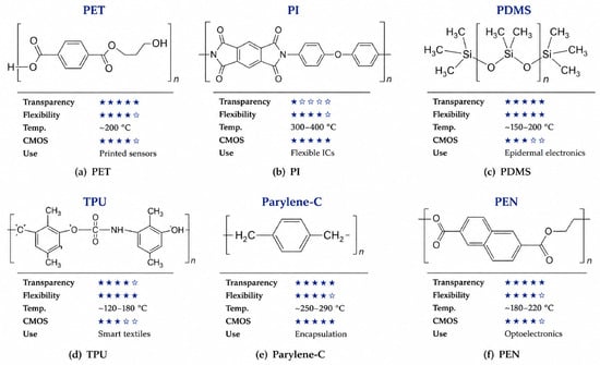
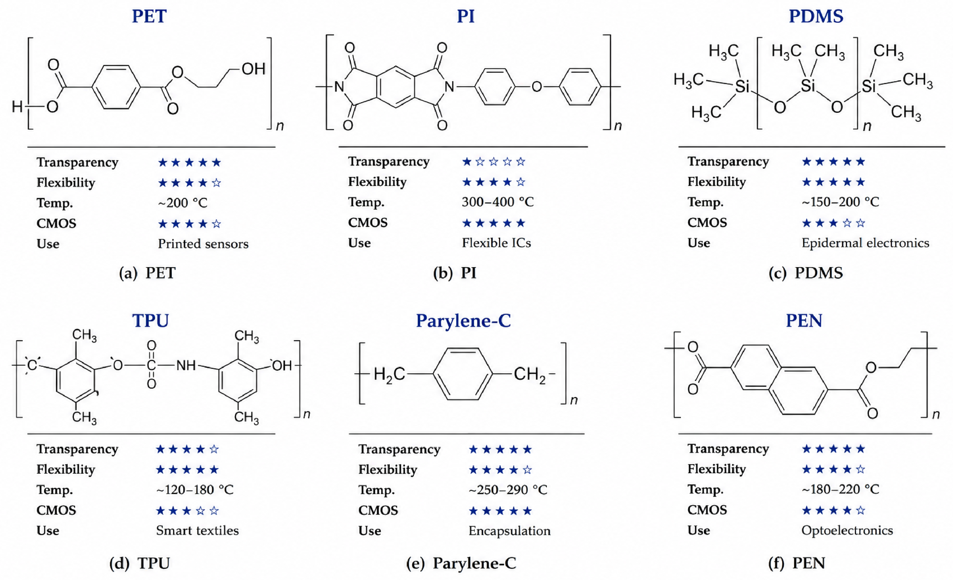
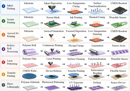
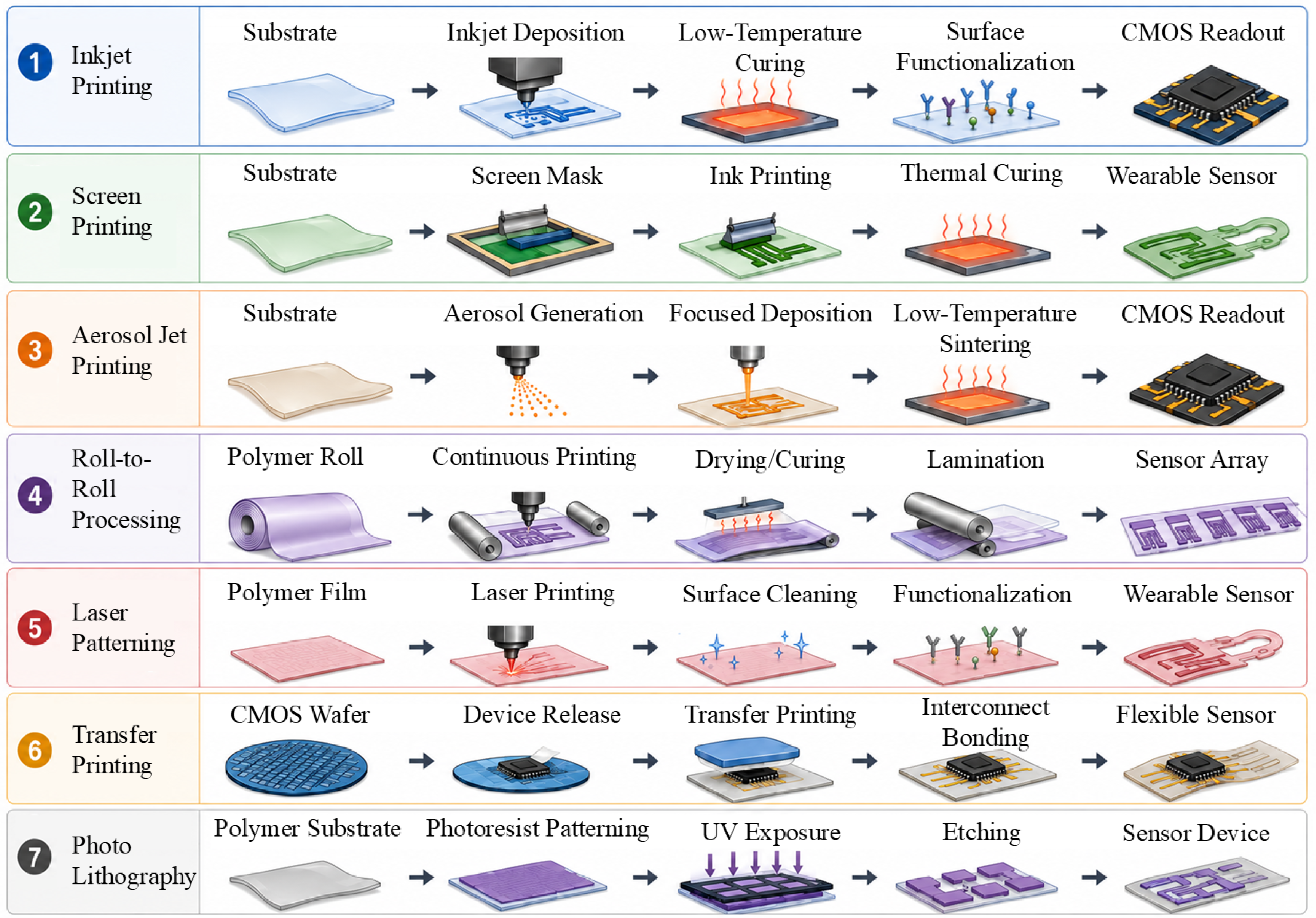
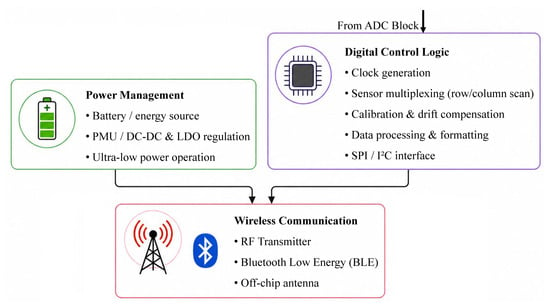
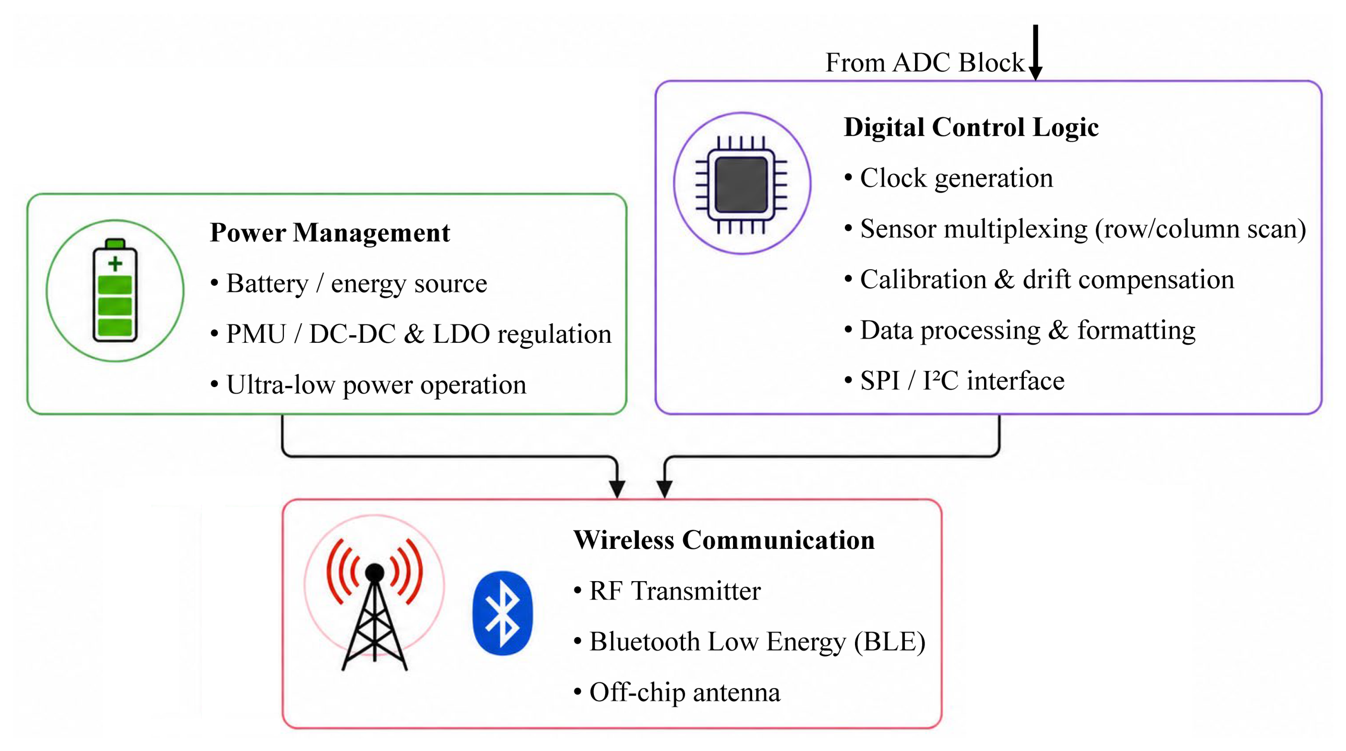
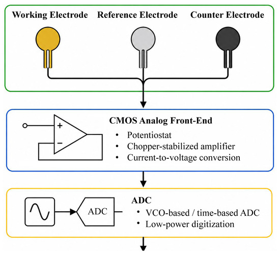
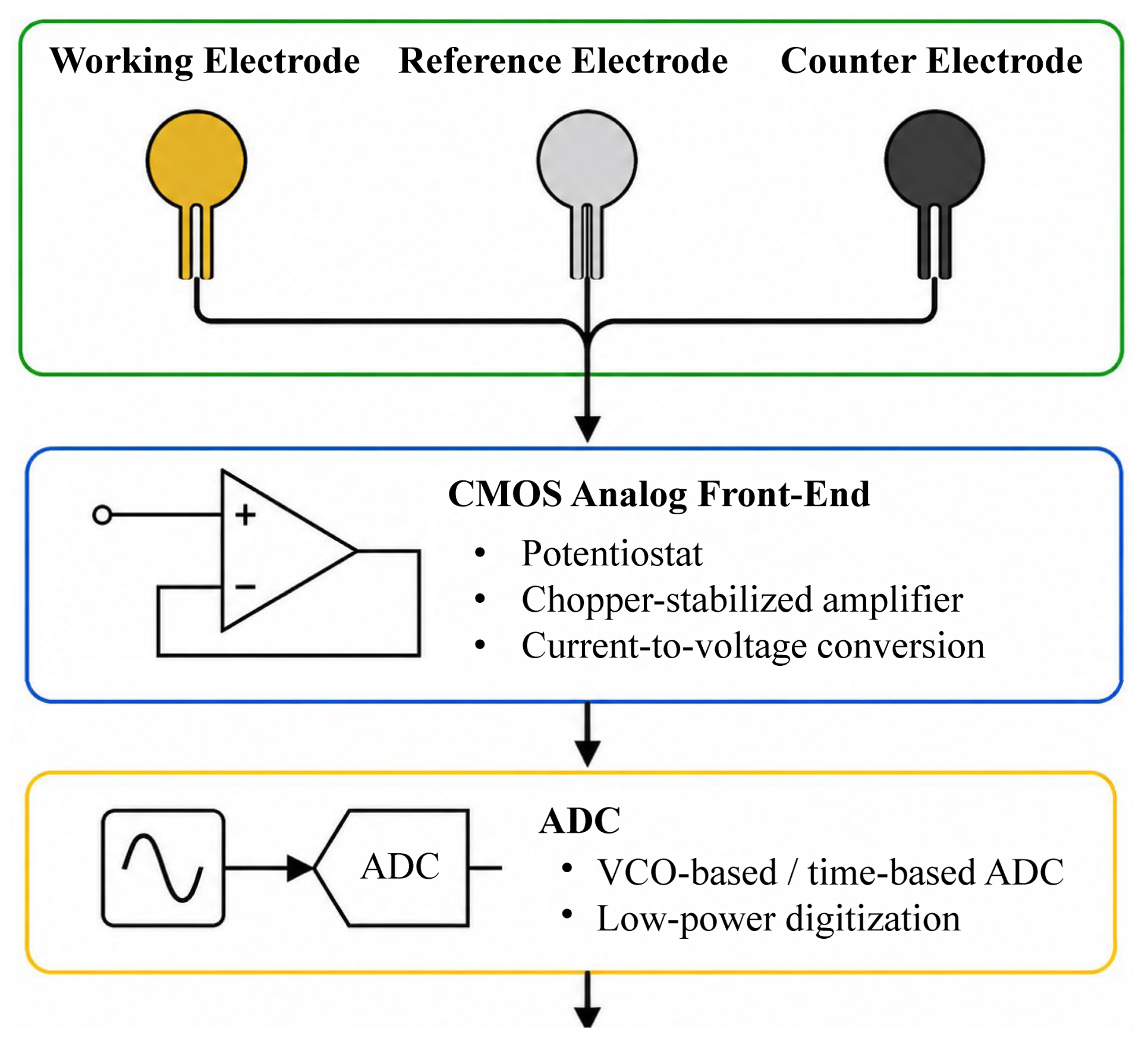
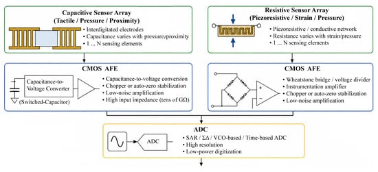
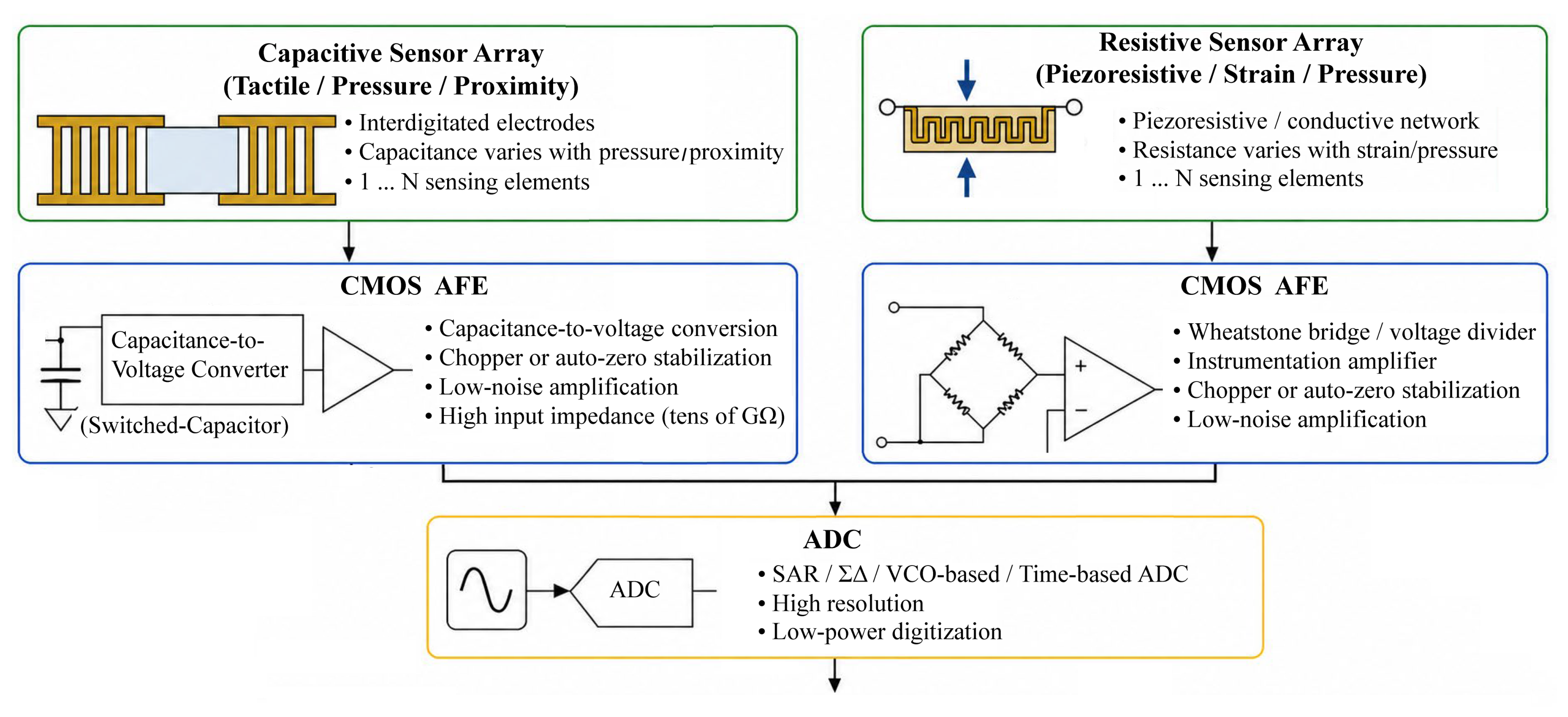
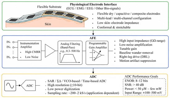
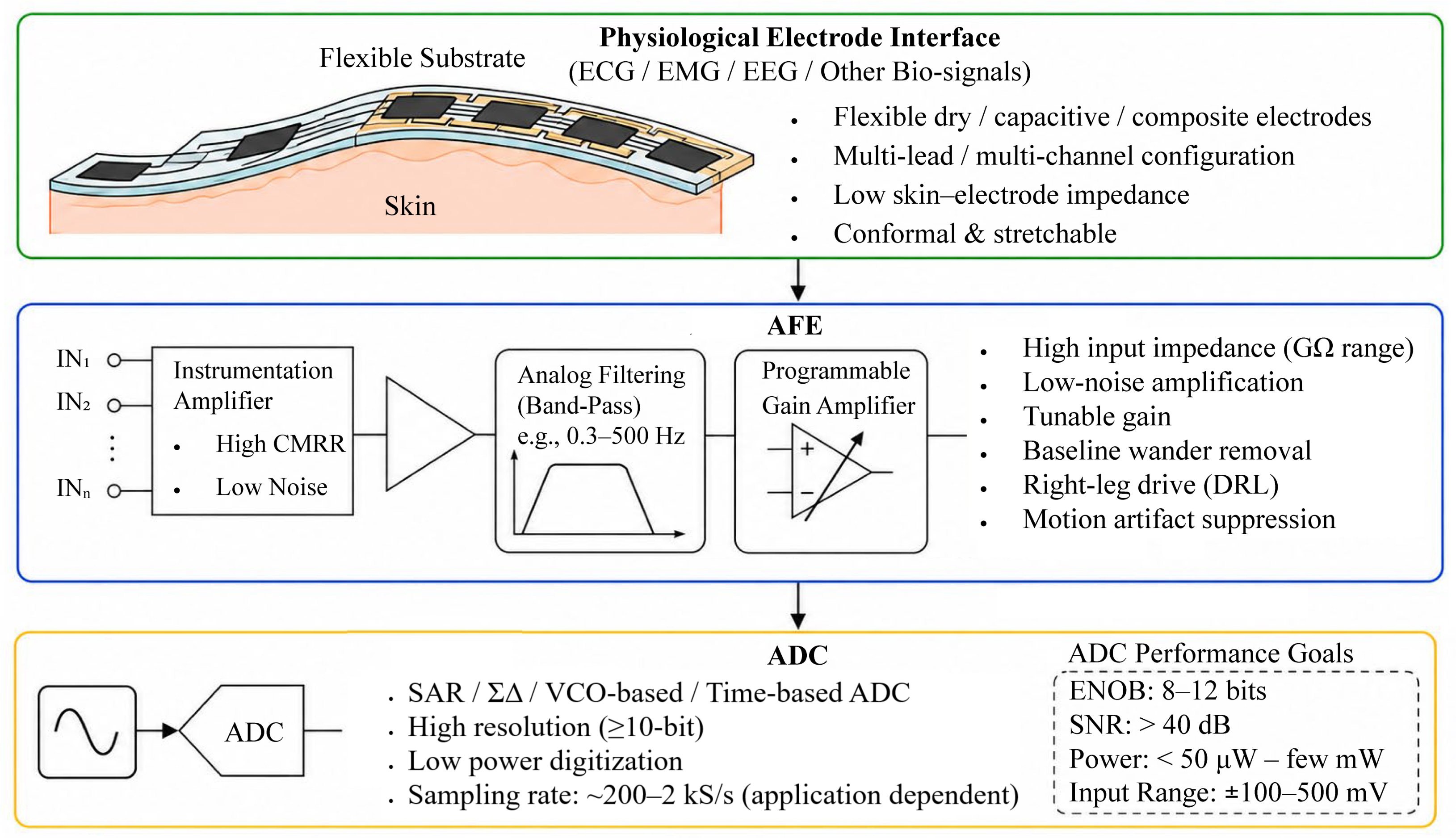

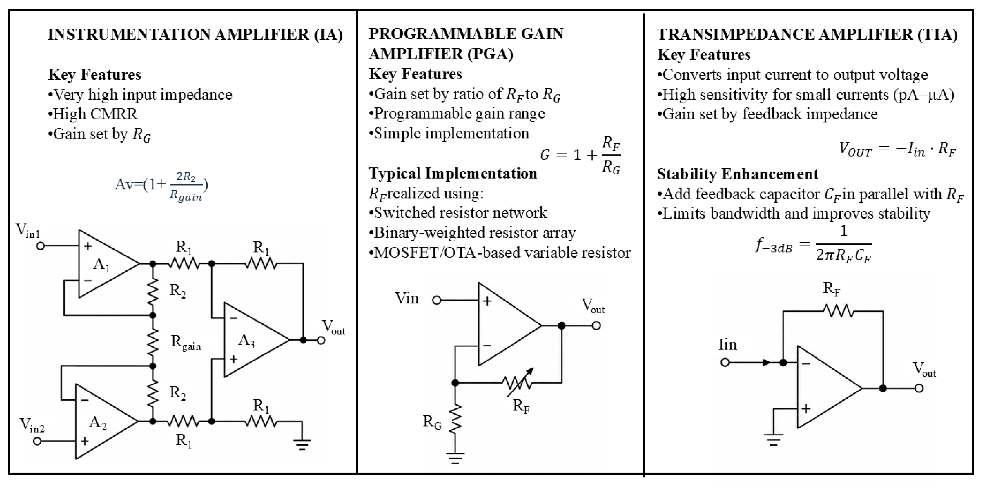
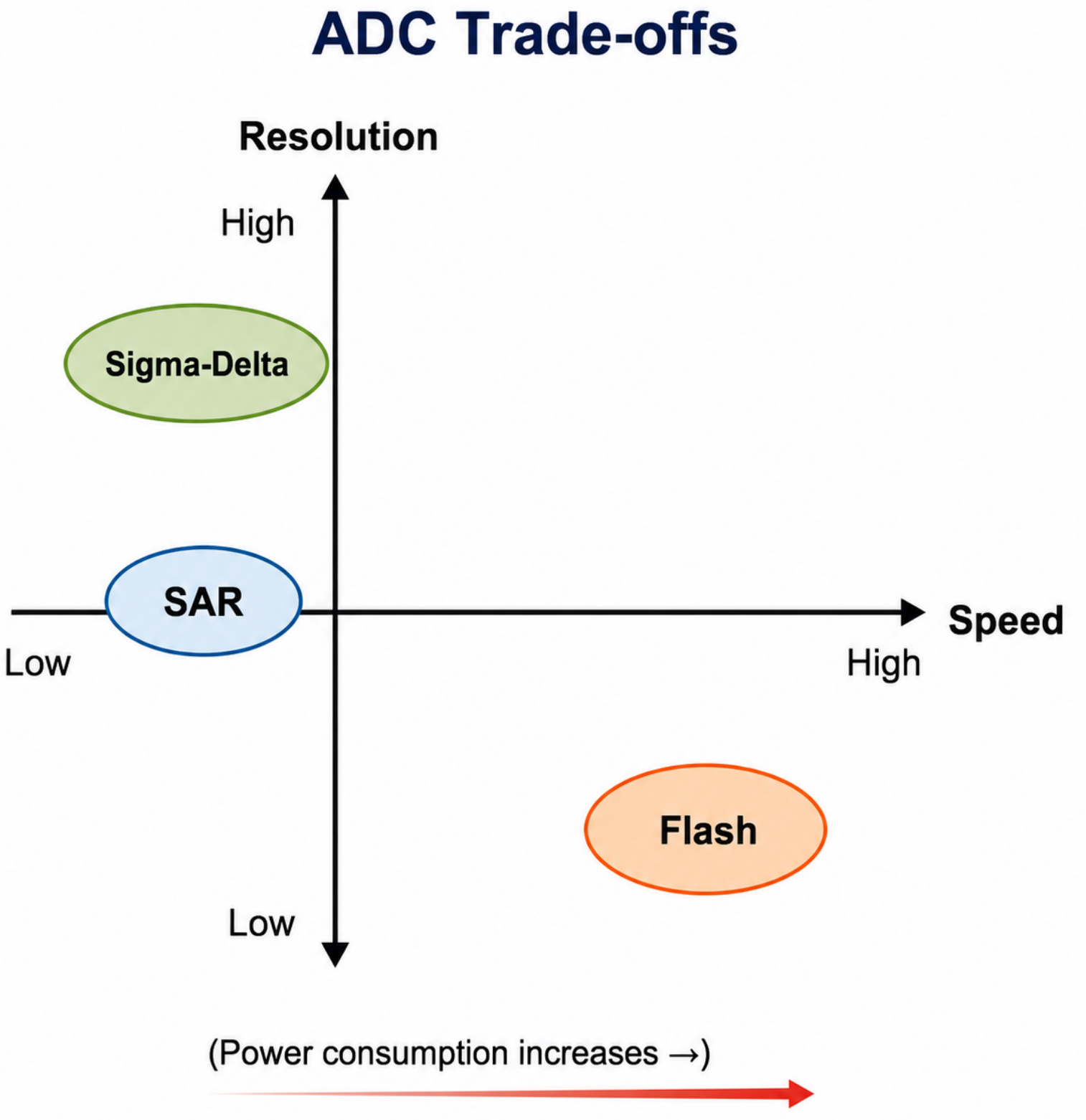
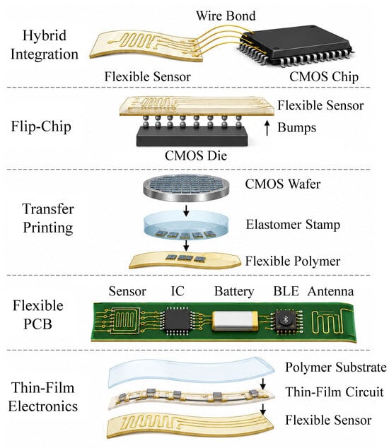
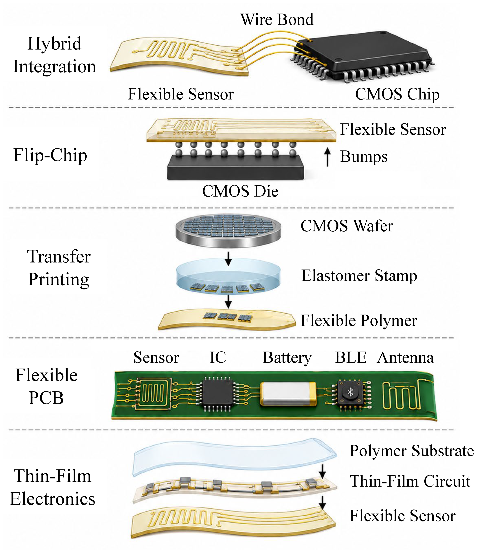

Disclaimer/Publisher’s Note: The statements, opinions and data contained in all publications are solely those of the individual author(s) and contributor(s) and not of MDPI and/or the editor(s). MDPI and/or the editor(s) disclaim responsibility for any injury to people or property resulting from any ideas, methods, instructions or products referred to in the content. |
© 2026 by the authors. Licensee MDPI, Basel, Switzerland. This article is an open access article distributed under the terms and conditions of the Creative Commons Attribution (CC BY) license.