


Abstract
A multifunctional circuit with high-pass and low-pass negative group delays can be achieved by simply changing the values of the components in the circuit, without changing the circuit structure. While achieving negative group delay, the circuit also has flat broadband characteristics and lower losses. Theoretical calculations and equation derivation are provided. The experimental circuit was simulated, and the simulation results were essentially consistent with the theoretical results, indicating the feasibility of the experiment.
1. Introduction
Group delay is an important technical indicator in identifying whether a communication system is in good condition, and distortion of group delay can cause some problems, such as increased system error rates. The negative group delay circuit, as a method of balancing group delay, has received a lot of attention.
Since the discovery of the theory of negative group delay, scholars have conducted extensive research on negative group delay circuits and proposed different circuit structures with negative group delay to meet different needs, such as the crab shape, Li type, etc. [1,2,3,4]. This includes lumped parameter circuits and microstrip line circuits. After proposing different circuit structures, scholars conducted theoretical analyses on negative group delay circuits [5,6,7]. At the same time, scholars have attempted to apply different negative group delay circuits in different fields, such as filters [8,9], non-Foster capacitors [10], cables [11], and improving array antenna performance [12,13,14] to eliminate the positive group delay generated by signals passing through communication systems.
Over time, scholars have found that there are usually significant fluctuations in circuit performance when negative group delay occurs. Therefore, the question of how to obtain a flat negative group delay to achieve ultra-low bit error rates in communication has become an important direction of negative group delay research [15]. In Ref. [16], a negative group delay circuit composed of microstrip lines is proposed. With a negative group delay of −1.11 ns and an insertion loss of 9.75 dB, the flat NGD bandwidth is 6.1% and the group delay fluctuation is 11.5%. In the study of flat negative group delay circuits, many scholars use a fluctuation of 8% as the standard [17,18], with a negative group delay of about −0.5 ns and insertion loss of over 15 dB under this standard. Similarly, many scholars use a fluctuation of 20% as the standard, which, as shown in [19], has a negative group delay of −0.2 ns and an insertion loss of 14 dB.
These flat circuit structures can usually only achieve one function. In Ref. [9], a circuit structure with three functions—low pass, high pass, and band pass—is proposed. However, the negative group delay that it achieves is not smooth, and, in research on flatness, it has significant insertion losses. Therefore, it is necessary to develop a multifunctional and low-loss flat negative group delay circuit.
This study proposes a flat negative group delay low-loss circuit that can achieve both high-pass and low-pass functions by changing the circuit component parameters. This article consists of four sections. The second section mainly describes the circuit structure and theoretically analyzes the circuit transfer function and group delay. It explores the impact of delay component parameters on the circuit when implementing a high-pass or low-pass negative group. The third section presents the circuit theory and simulation results and compares them with other research results to demonstrate that the circuit has the advantages of high-pass and low-pass flat negative group delay. The final section presents the conclusions of the study.
2. Circuit Design and Analysis with High-Pass and Low-Pass Negative Group Delay
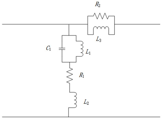
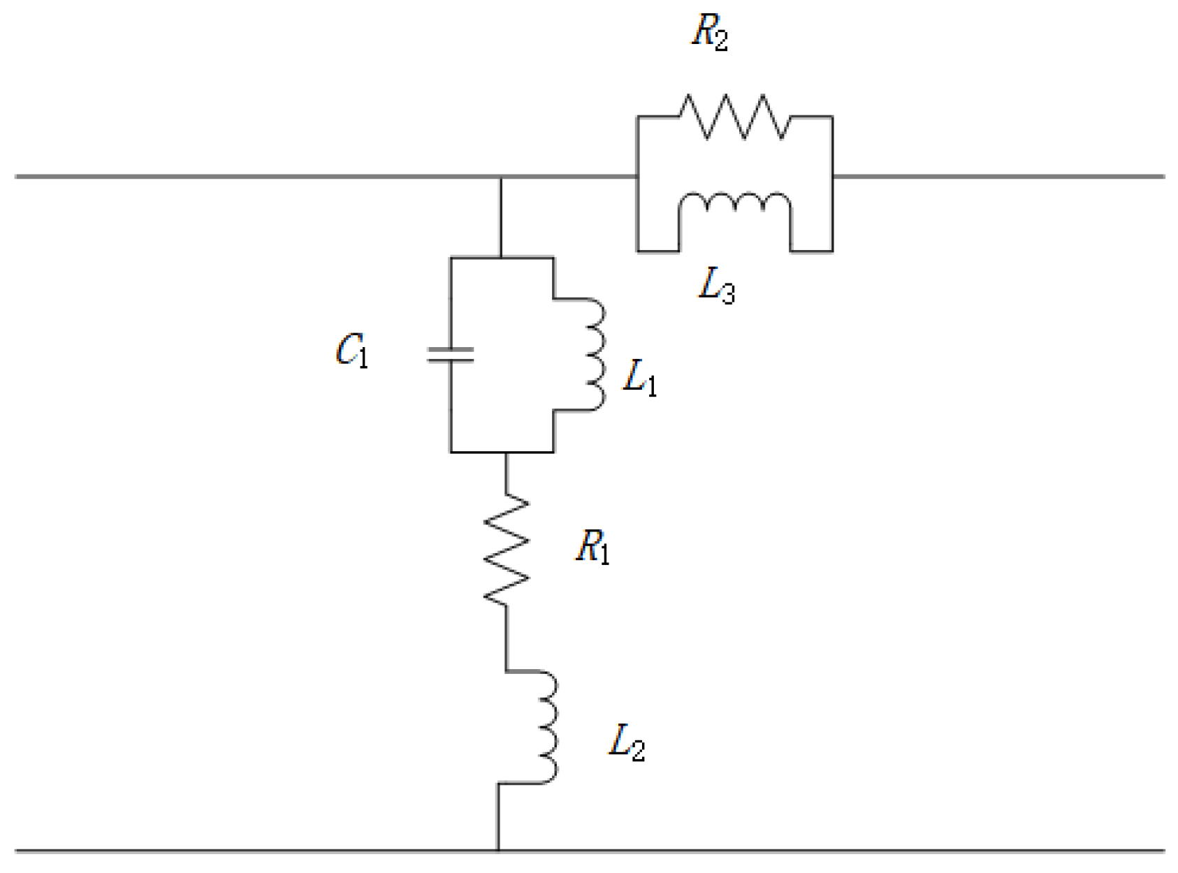
As shown in Figure 1, the circuit that can achieve high-pass and low-pass negative group delays is composed of a branch connected in series with a capacitor C1 and in parallel with an inductor L1, resistor R1, and inductor L2, and then connected in series with a branch connected in parallel with a resistor R2 and inductor L3. The topology retains the structural characteristics of both the high-pass prototype and the low-pass prototype, and the circuit can be switched between low pass and high pass by adjusting the parameters of the components in the circuit. By changing the values of capacitors C1, inductors L3, L2, and resistors R1, R2, the circuit can have the function of a high-pass or low-pass flat negative group delay circuit. Compared with previously designed negative group delay circuits, the negative group delay circuit designed in this work can achieve high-pass negative group delay while maintaining fairly high flatness.
Figure 1.
Negative group delay circuit structure diagram.
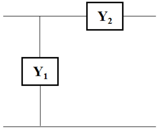
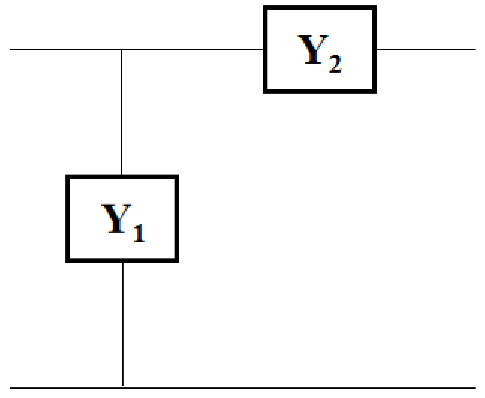
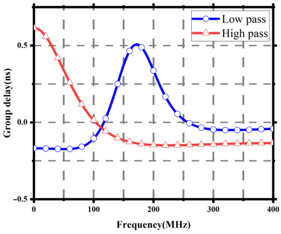
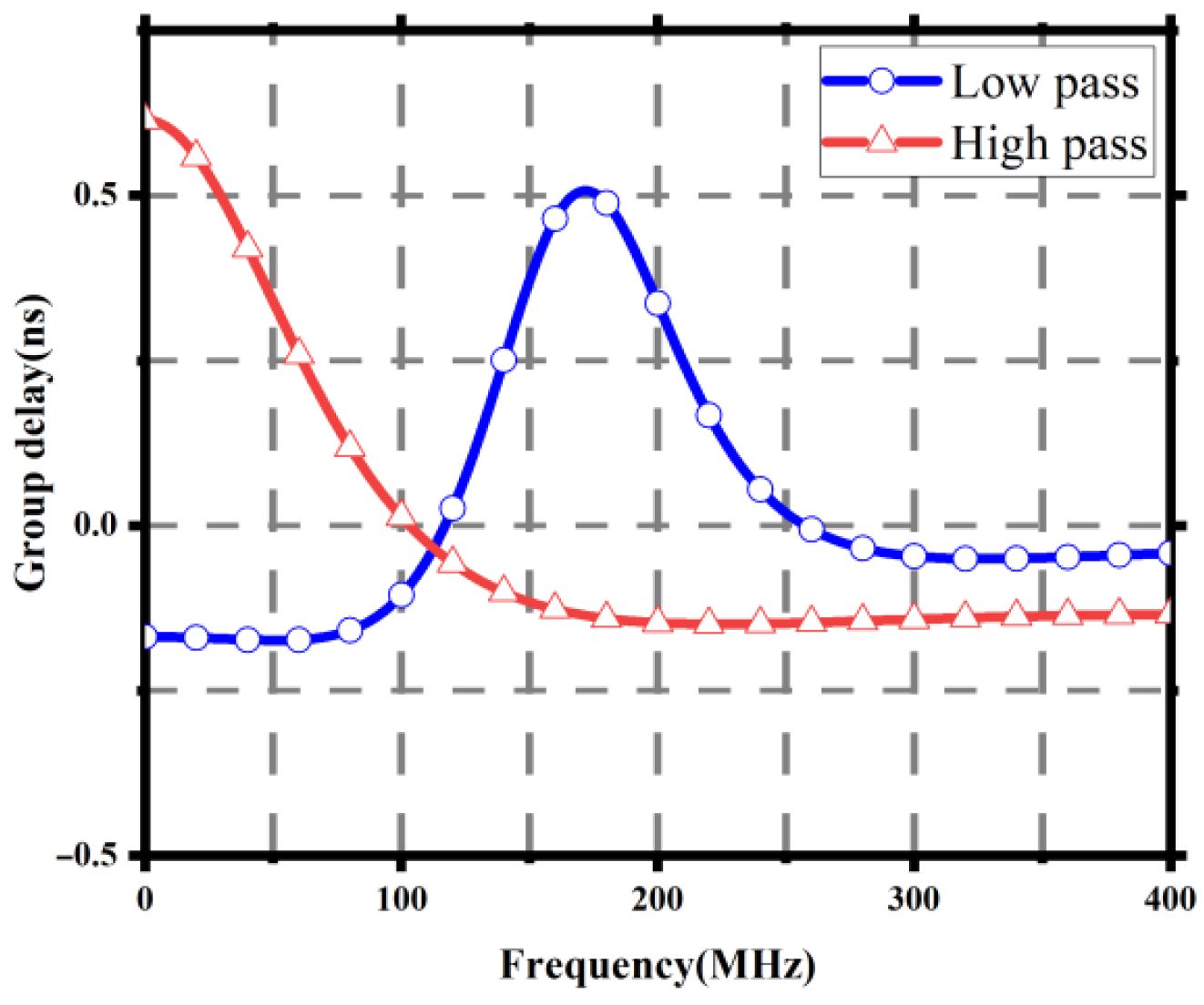
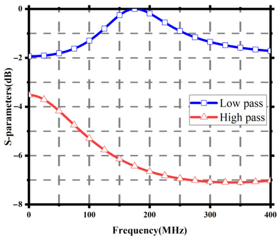
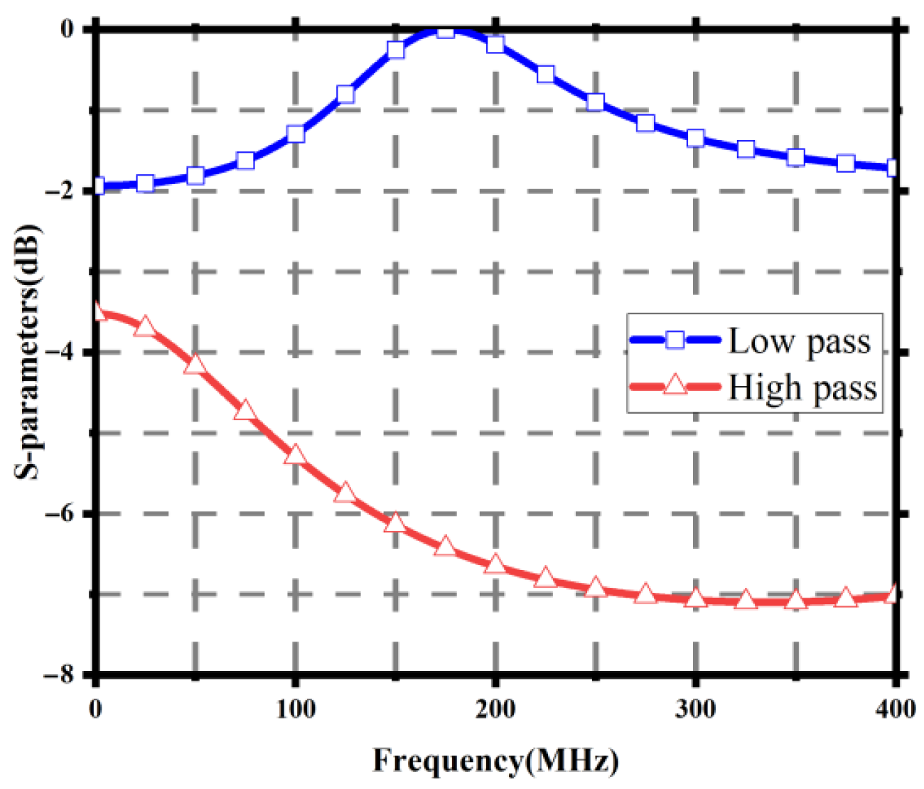
The impedance value of the circuit is given in Equation (1), and the equivalent [ABCD] matrix model is shown in Figure 2. The [ABCD] matrix value of the circuit is also given in Equation (2). Moreover, the partial admittance of the circuit is given in Equations (3) and (4). By synthesizing Equations (2)–(4), the transfer function of the circuit can be obtained, as given in Equations (5) and (6), and the group delay is given in Equation (7). The results of achieving high-pass and low-pass negative group delays in the circuit are shown in Figure 3 and Figure 4.
Figure 2.
Equivalent [ABCD] matrix model.
Figure 3.
The group delay result generated by the circuit shown in Figure 1.
Figure 4.
The S21 result generated by the circuit shown in Figure 1.
2.1. High-Pass Flat Negative Group Delay Circuit
The circuit structure is shown in Figure 1. When the values of the components in the circuit are as shown in Table 1, the circuit is a circuit with a high-pass negative group delay function. The results are shown by the red lines in Figure 3 and Figure 4.
Table 1.
Component values for high-pass flat negative group delay low-loss circuit.
2.1.1. High-Pass Negative Group Delay Circuits with Different C1 Values
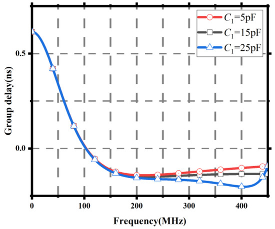
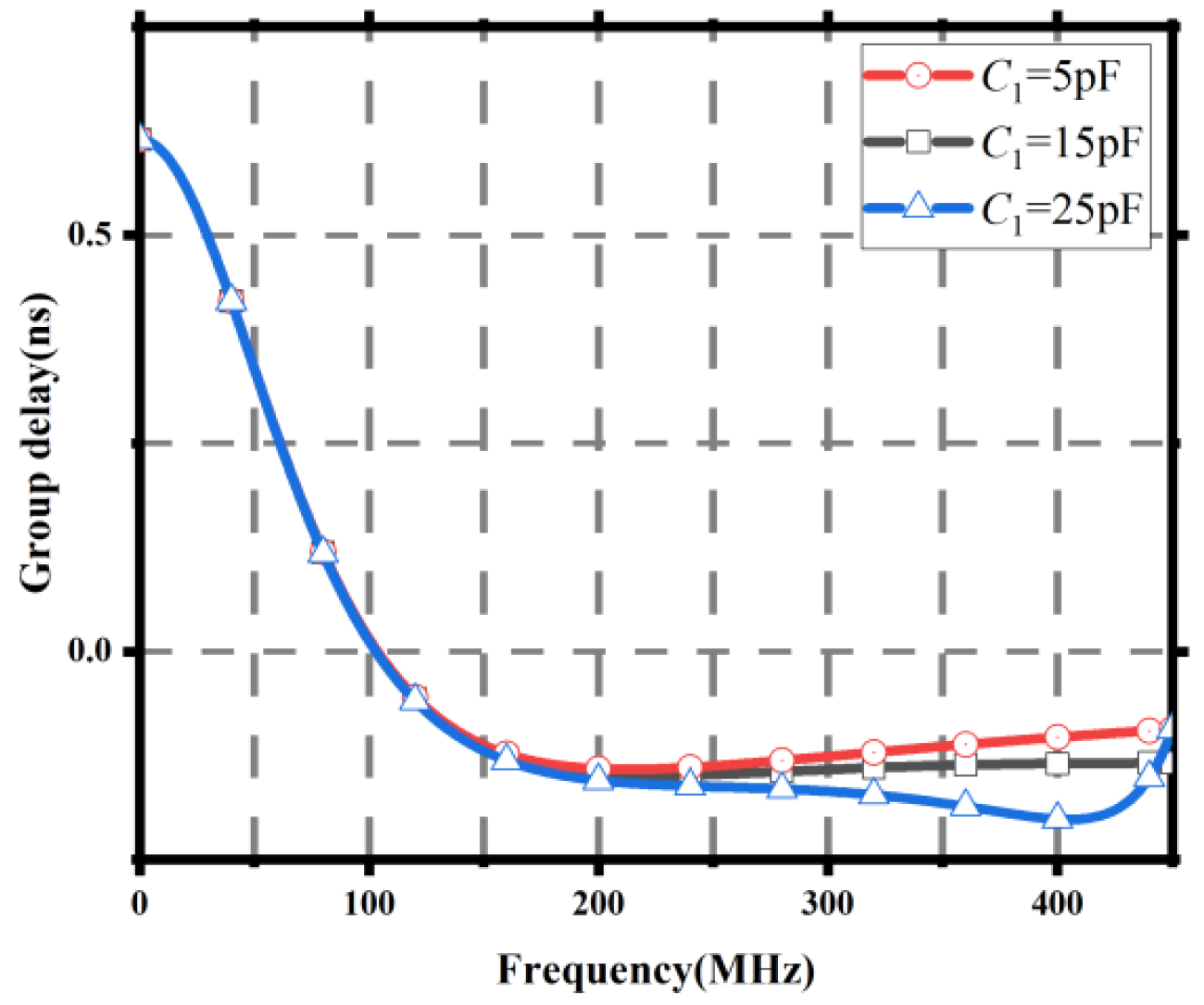
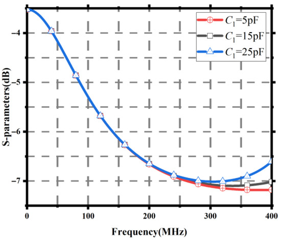
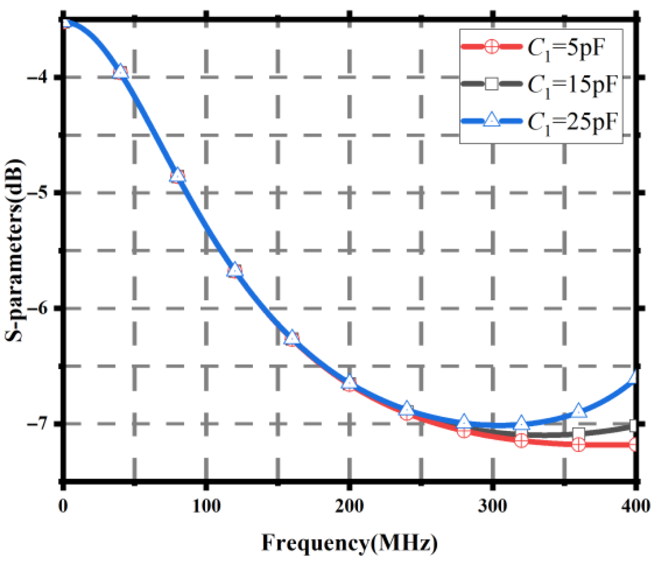
When the values of 1, R1, 2, 2, and 3 in the circuit remain unchanged, as shown in Table 1, we change the values of 1 to 5 pF, 15 pF, and 25 pF in sequence and observe the changes in the circuit transfer function and group delay. The circuit results in these three cases are shown in Table 2 and Figure 5 and Figure 6. Through observation, it is found that changing the value of capacitor 1 does not change the group delay of the high-pass circuit at 0 MHz. However, as the frequency increases, the larger the value of capacitor 1, the greater the negative group delay value. The change in capacitor 1 also affects the flat negative group delay bandwidth. If the capacitance is too large or too small, the negative group delay will not have a relatively flat characteristic, and the circuit insertion loss will also decrease with the increase in capacitor 1. 1 is the key capacitive element of a high-pass negative group delay circuit, and changes in its value modify the circuit’s impedance characteristics and energy transfer efficiency. When 1 is increased, the impedance matching and resonance characteristics of the branch in the circuit formed by the participation are changed, resulting in a reduction in the energy attenuation of the signal as it is transmitted through the circuit, which in turn manifests itself as a reduction in the loss of insertion (IL).
Table 2.
Circuit results with different 1 values.
Figure 5.
Group delay results for different 1 values.
Figure 6.
21 results for different 1 values.
2.1.2. High-Pass Negative Group Delay Circuits with Different L1 Values
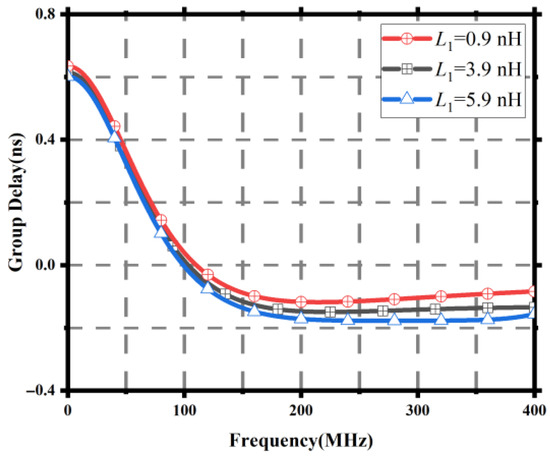
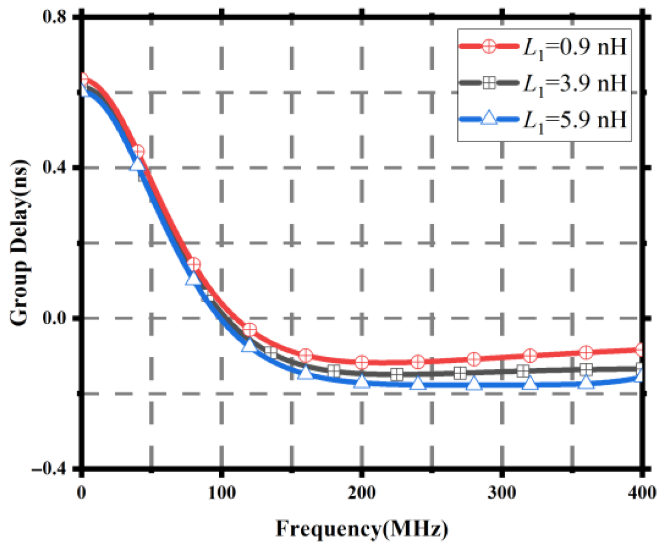
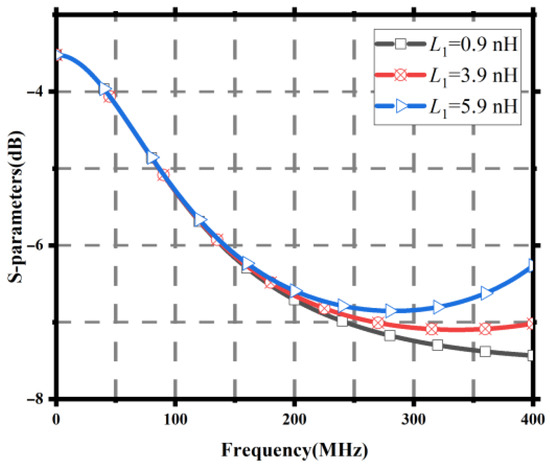
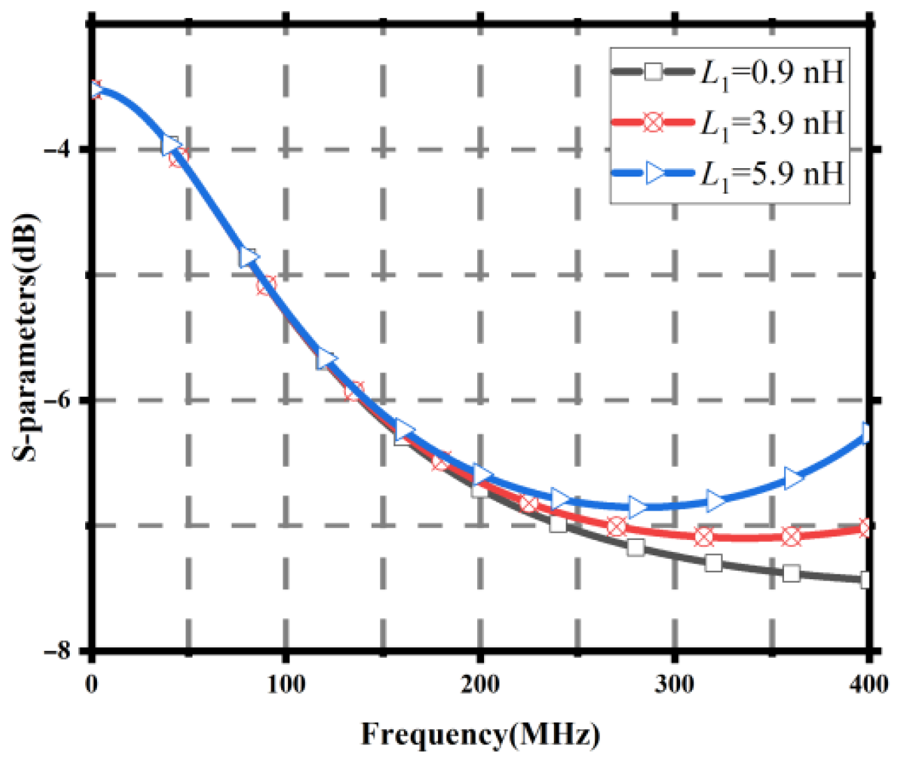
When the values of 1, 1, 2, 2, and 3 in the circuit remain unchanged, as shown in Table 1, we change the values of 1 to 0.9 nH, 3.9 nH, and 5.9 nH in sequence and observe the changes in the circuit transfer function and group delay. The circuit results in these three scenarios are shown in Table 3 and Figure 7 and Figure 8. Through observation, it is found that, as the value of inductance 1 increases, the group delay of the high-pass circuit at 0 MHz decreases. As the frequency increases, the larger the value of capacitance 1, the smaller the negative group delay value. The change in inductance 1 also affects the flat negative group delay bandwidth, and the insertion loss of the circuit also decreases with the increase in inductance 1.
Table 3.
Circuit results with different 1 values.
Figure 7.
Group delay results for different 1 values.
Figure 8.
21 results for different 1 values.
2.1.3. High-Pass Negative Group Delay Circuits with Different R1 Values
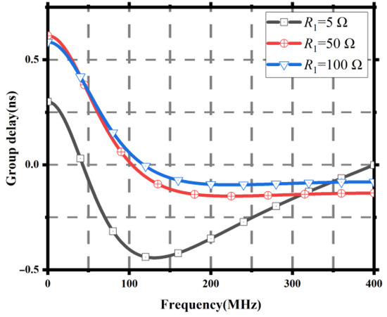
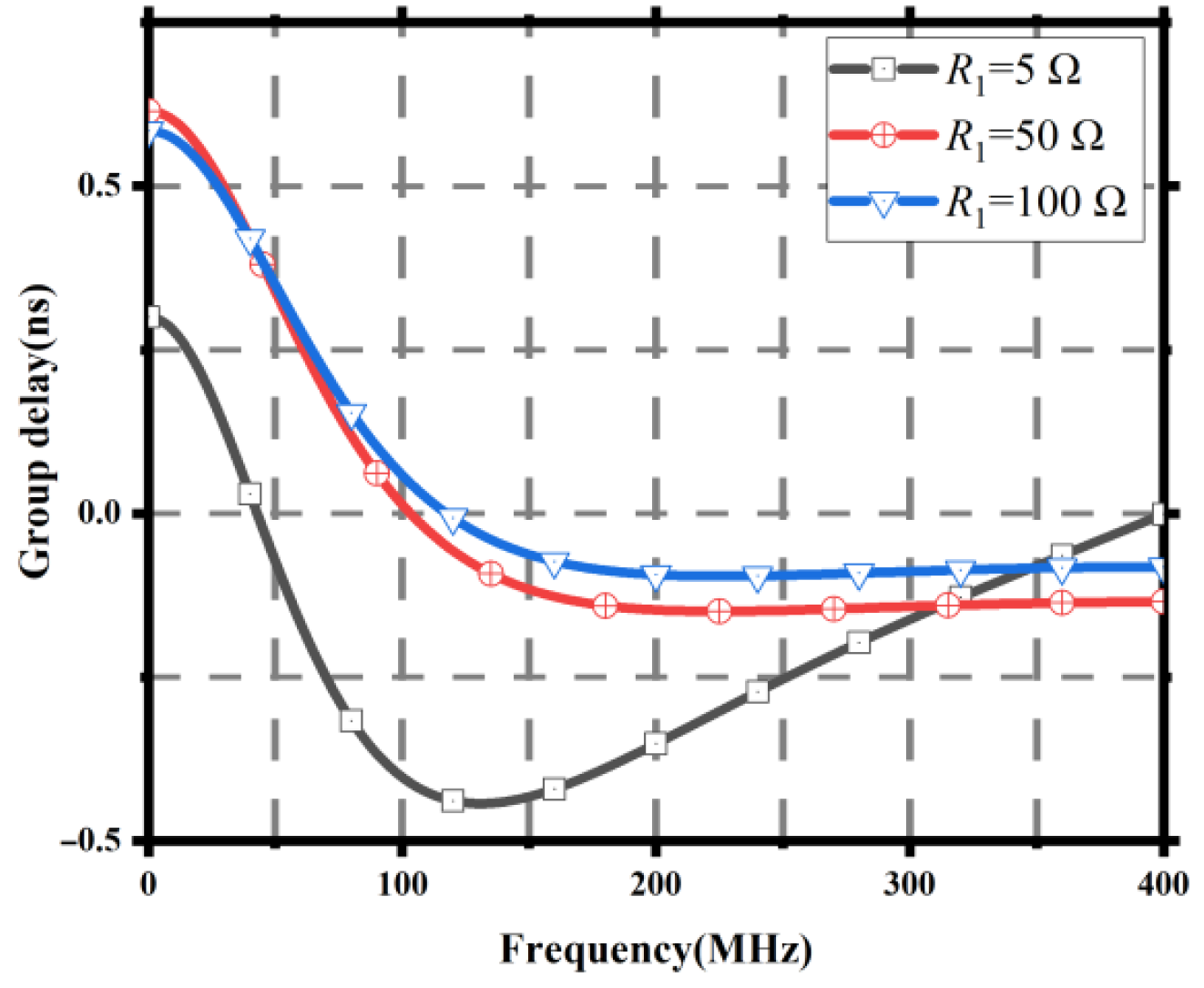
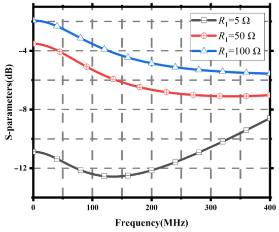
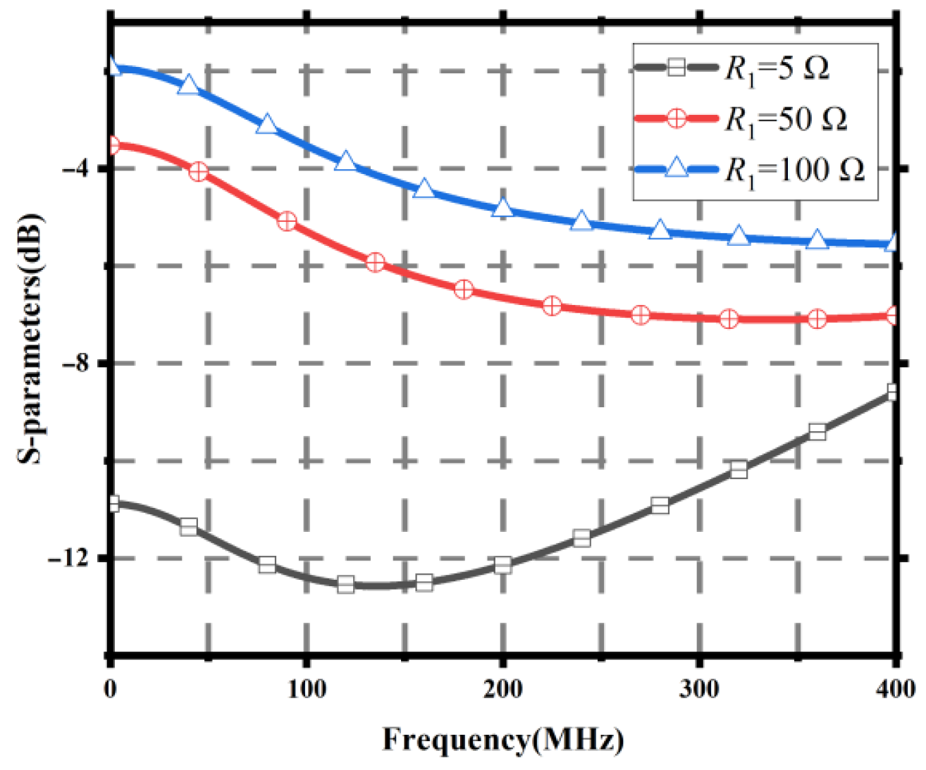
When the values of 1, 1, 2, 2, and 3 in the circuit remain unchanged from Table 1, we change the values of R1 to 10 Ω, 50 Ω, and 100 Ω in sequence and observe the changes in the circuit transfer function and group delay. The circuit results in these three cases are shown in Table 4 and Figure 9 and Figure 10. Through observation, it is found that, as the value of resistance 1 decreases, the negative group delay value of the circuit is no longer flat. However, as 1 decreases, the minimum negative group delay of the high-pass circuit decreases, and the circuit insertion loss also decreases with the increase in resistance 1.
Table 4.
Circuit results with different 1 values.
Figure 9.
Group delay results for different 1 values.
Figure 10.
21 results for different 1 values.
2.1.4. High-Pass Negative Group Delay Circuits with Different L2 Values
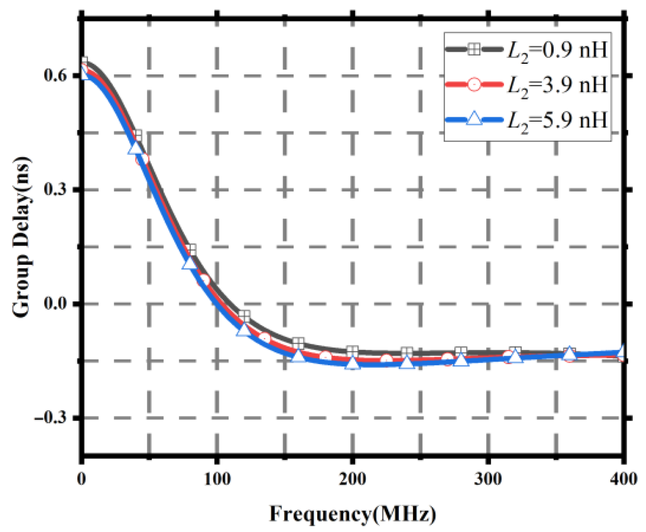
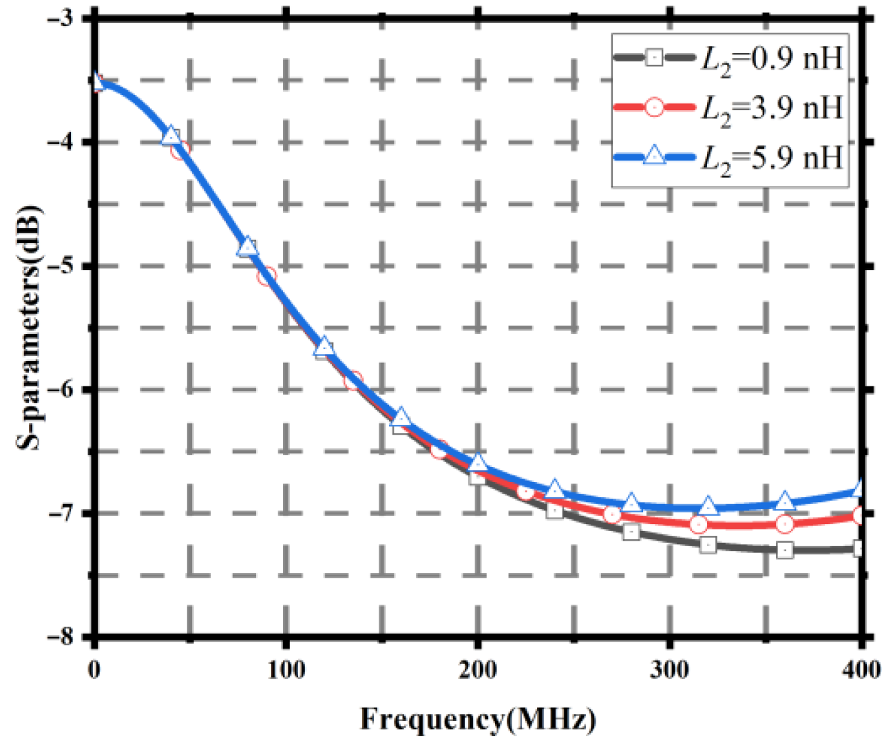
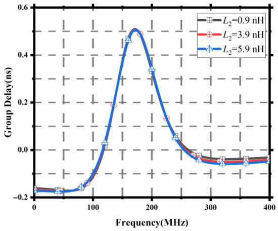
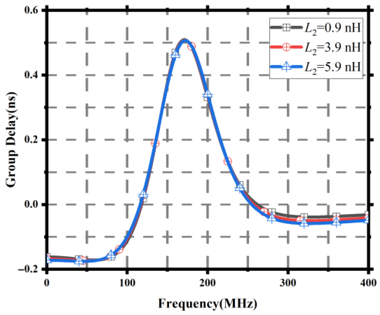
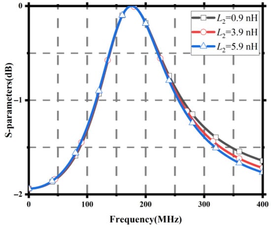
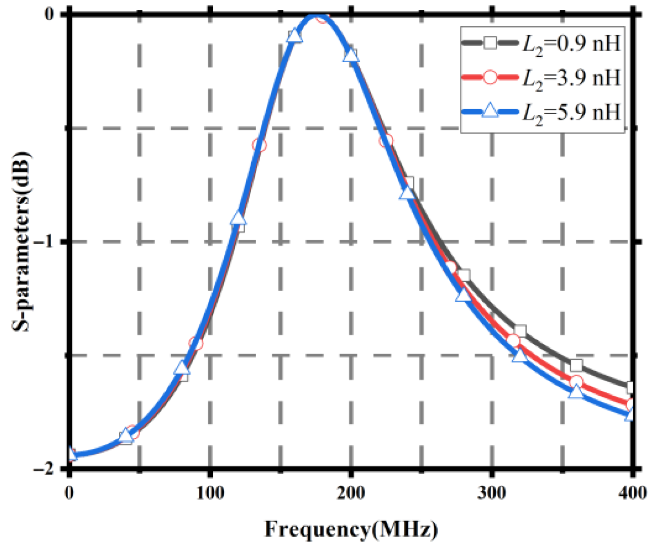
When the values of C1, R1, L1, R2, and L3 in the circuit remain unchanged, as shown in Table 1, and the L2 values are sequentially changed to 0.9 nH, 3.9 nH, and 5.9 nH, we observe the changes in the circuit transfer function and group delay. The circuit results in these three scenarios are shown in Table 5 and Figure 11 and Figure 12. Through observation, it is found that, as the value of inductance L2 increases, the group delay of the high-pass circuit at 0 MHz decreases, but the difference is small. Changing the value of inductance L2 also has a small impact on the bandwidth of the flat negative group delay. At the same time, the insertion loss of the circuit also decreases with the increase in inductance L2.
Table 5.
Circuit results with different 2 values.
Figure 11.
Group delay results for different 2 values.
Figure 12.
21 results for different 2 values.
2.1.5. High-Pass Negative Group Delay Circuits with Different 2 Values
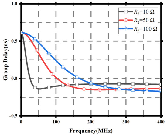
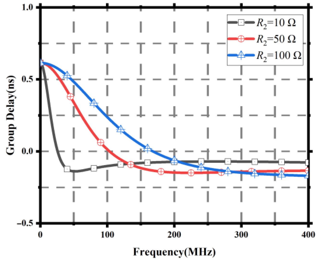
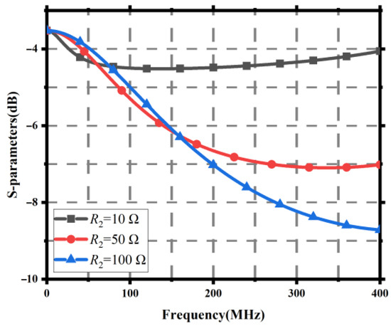
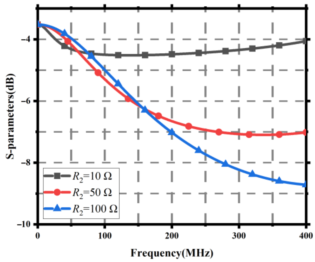
When the values of 1, 1, 2, 1, and 3 in the circuit remain unchanged, as shown in Table 1, and the 2 values are sequentially changed to 10 Ω, 50 Ω, and 100 Ω, we observe the changes in the circuit transfer function and group delay. The circuit results in these three cases are shown in Table 6 and Figure 13 and Figure 14. Through observation, it is found that the group delay of the high-pass circuit remains unchanged at 0 MHz as the resistance 2 value changes. However, increasing or decreasing 2 will lead to poorer flatness of the high-pass circuit. The negative group delay value will also decrease as 2 decreases, and the insertion loss of the circuit will also increase with the increase in resistance 2.
Table 6.
Circuit results with different 2 values.
Figure 13.
Group delay results for different 2 values.
Figure 14.
21 results for different 2 values.
2.1.6. High-Pass Negative Group Delay Circuits with Different 3 Values
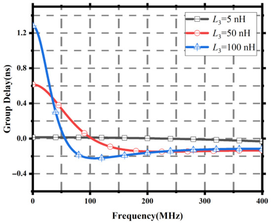
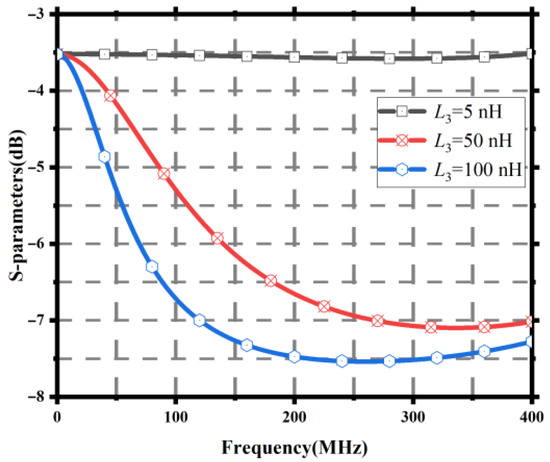
When the values of 1, 1, 1, 2, and 2 in the circuit remain unchanged from Table 1, we change the values of 3 to 5 nH, 50 nH, and 100 nH in sequence and observe the changes in the circuit transfer function and group delay. The circuit results in these three cases are shown in Table 7 and Figure 15 and Figure 16. Through observation, it is found that, as the value of inductance 3 increases, the group delay of the high-pass circuit at 0 MHz increases. As the value of inductance 3 increases, the negative group delay value decreases, and the circuit insertion loss increases with the increase in inductance 3.
Table 7.
Circuit results with different 3 values.
Figure 15.
Group delay results for different 3 values.
Figure 16.
21 results for different 3 values.
2.2. Low-Pass Flat Negative Group Delay Circuit
The circuit structure is shown in Figure 1. When the values of the components in the circuit are as shown in Table 8, the circuit has a low-pass negative group delay function, as shown by the blue lines in Figure 3 and Figure 4.
Table 8.
Component values for low-pass flat negative group delay low-loss circuit.
2.2.1. Low-Pass Negative Group Delay Circuits with Different C1 Values
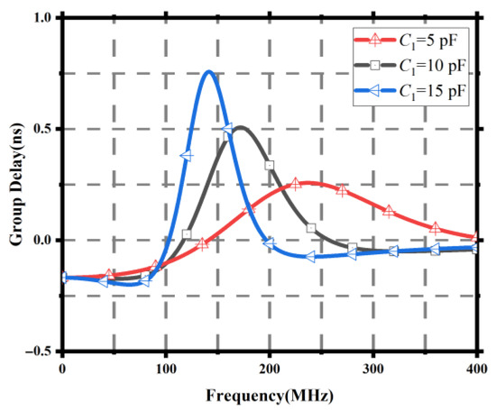
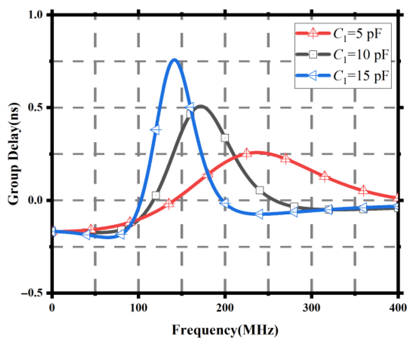
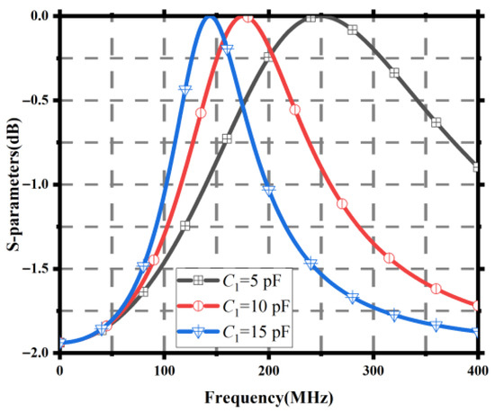
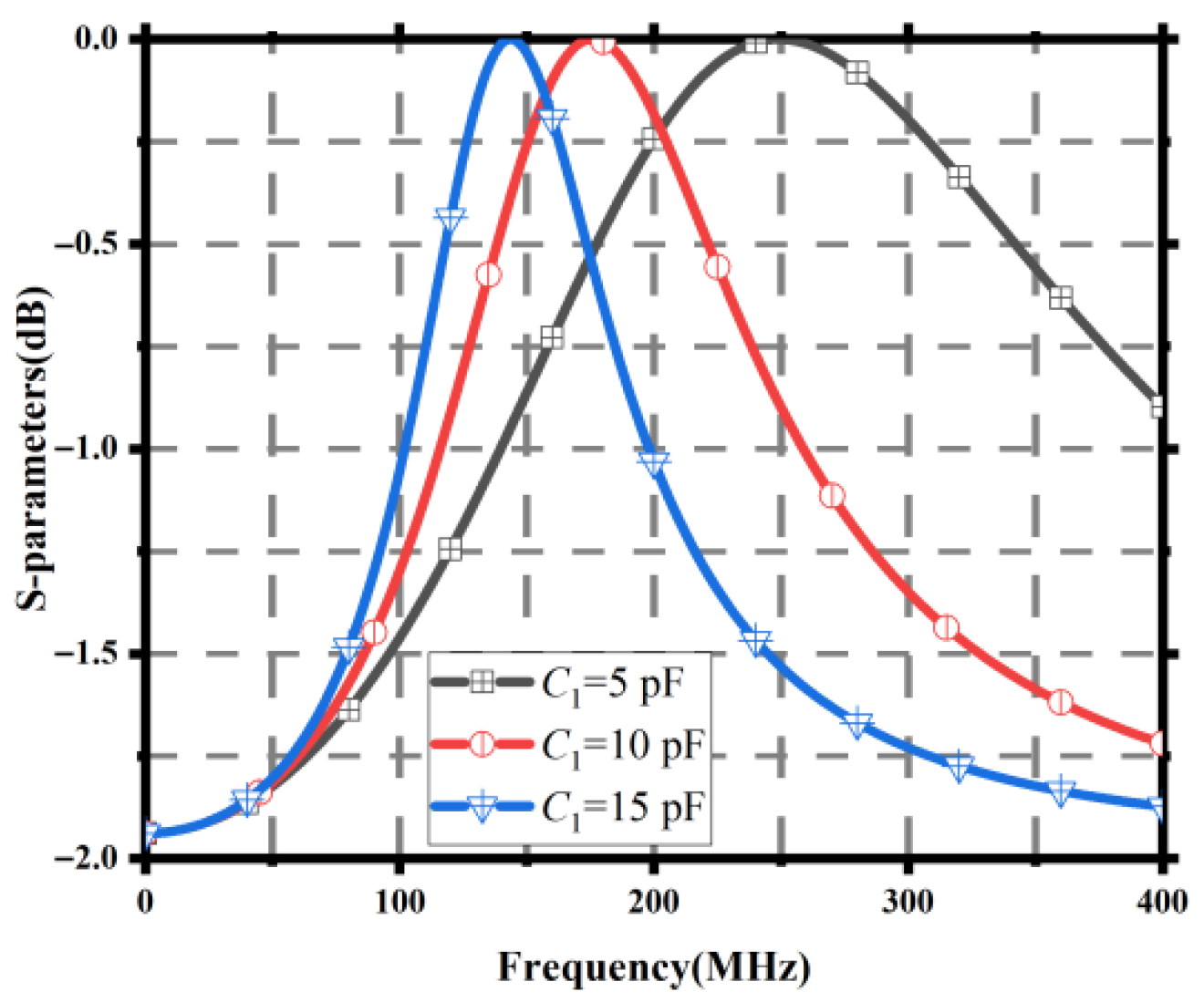
When the values of L1, R1, L2, R2, and L3 in the circuit remain unchanged, as shown in Table 8, and the values of C1 are sequentially changed to 5 pF, 10 pF, and 15 pF, we observe the changes in the circuit transfer function and group delay. The circuit results in these three cases are shown in Table 9 and Figure 17 and Figure 18. Through observation, it is found that changing the value of capacitor C1 does not change the group delay of the low-pass circuit at 0 MHz. However, as the frequency increases, the larger the value of capacitor C1, the smaller the negative group delay value. The change in capacitor C1 also affects the flat negative group delay bandwidth. If the capacitance is too large or too small, the negative group delay will not have a relatively flat characteristic, and the change in C1 does not affect the maximum insertion loss value of the circuit.
Table 9.
Circuit results with different 1 values.
Figure 17.
Group delay results for different 1 values.
Figure 18.
21 results for different 1 values.
2.2.2. Low-Pass Negative Group Delay Circuits with Different 1 Values
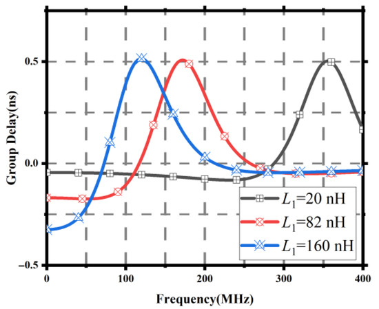
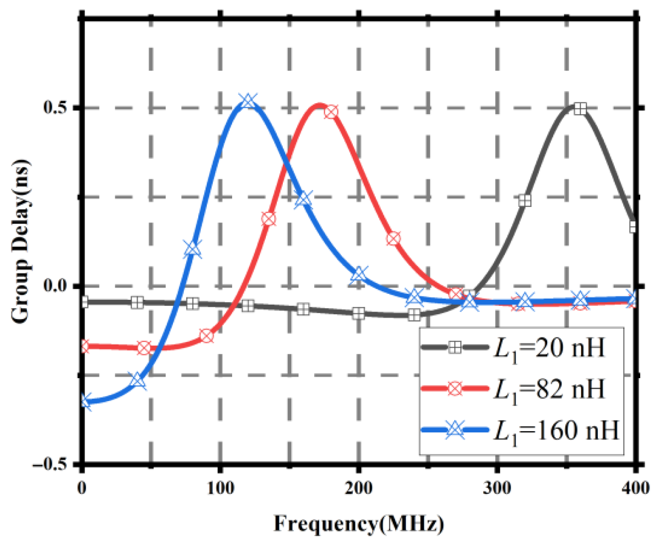
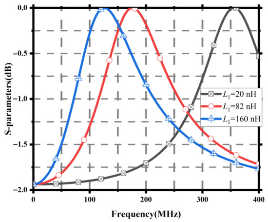
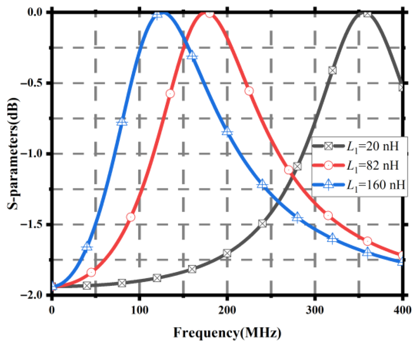
When the values of C1, R1, L2, R2, and L3 in the circuit remain unchanged, as shown in Table 8, and the L1 values are sequentially changed to 20 nH, 82 nH, and 160 nH, we observe the changes in the circuit transfer function and group delay. The circuit results in the three scenarios are shown in Table 10 and Figure 19 and Figure 20. Through observation, it is found that, as the value of inductance L1 increases, the group delay of the low-pass circuit at 0 MHz decreases, while the bandwidth of the flat negative group delay decreases. The circuit insertion loss does not change with the change in inductance L1.
Table 10.
Circuit results with different 1 values.
Figure 19.
Group delay results for different 1 values.
Figure 20.
21 results for different 1 values.
2.2.3. Low-Pass Negative Group Delay Circuits with Different R1 Values
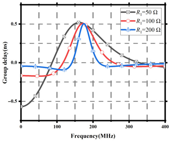
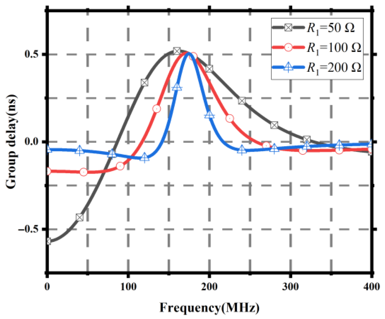
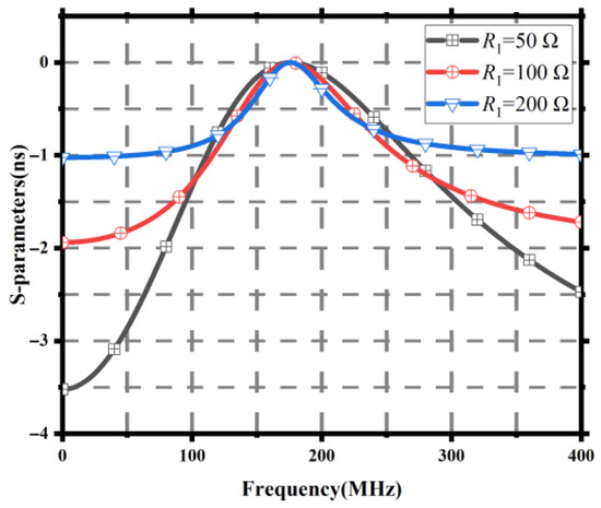
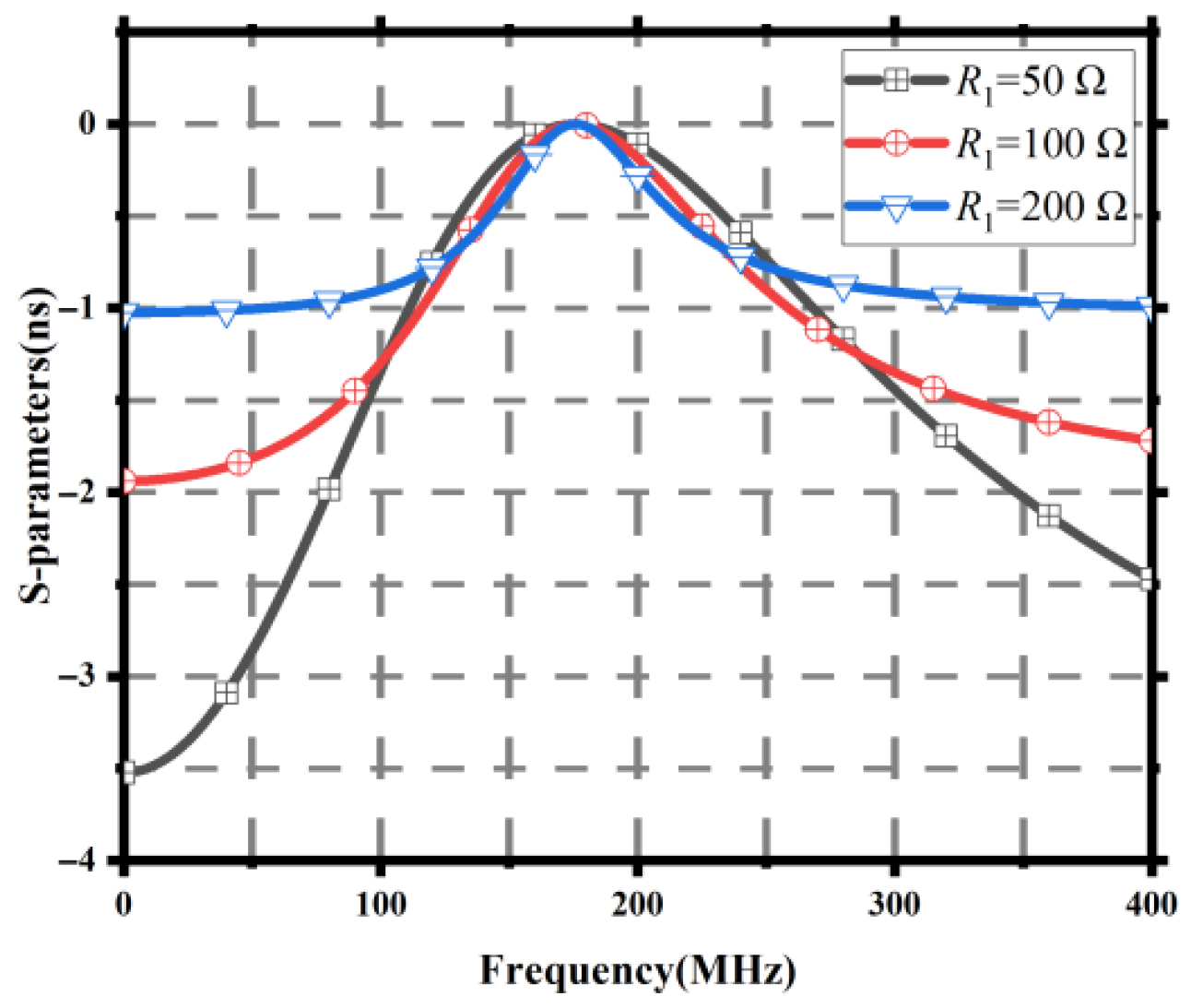
When the values of C1, L1, L2, R2, and L3 in the circuit remain unchanged, as shown in Table 8, we change the values of R1 to 50 Ω, 100 Ω, and 200 Ω in sequence and observe the changes in the circuit transfer function and group delay. The circuit results in these three cases are shown in Table 11 and Figure 21 and Figure 22. Through observation, it is found that, as the value of resistance R1 decreases, the negative group delay value of the circuit is no longer flat. However, as R1 decreases, the minimum negative group delay of the high-pass circuit decreases, and the circuit insertion loss also decreases with the increase in resistance R1.
Table 11.
Circuit results with different 1 values.
Figure 21.
Group delay results for different 1 values.
Figure 22.
21 results for different 1 values.
2.2.4. Low-Pass Negative Group Delay Circuits with Different L2 Values
When C1, R1, L1, R2, and L3 in the circuit remain unchanged from the values in Table 8, and the L2 values are sequentially changed to 0.9 nH, 3.9 nH, and 5.9 nH, we observe the changes in the circuit transfer function and group delay. The circuit results in the three scenarios are shown in Table 12 and Figure 23 and Figure 24. Through observation, it is found that, as the value of inductance L2 increases, the group delay of the high-pass circuit at 0 MHz decreases, but the difference is small. Changing the value of inductance L2 also has a small impact on the bandwidth of the flat negative group delay. At the same time, the insertion loss of the circuit does not change with the value of inductance L2.
Table 12.
Circuit results with different 2 values.
Figure 23.
Group delay results for different 2 values.
Figure 24.
21 results for different 2 values.
2.2.5. Low-Pass Negative Group Delay Circuits with Different 2 Values
When the values of C1, L1, L2, R1, and L3 in the circuit remain unchanged, as shown in Table 8, and the R2 values are sequentially changed to 50 Ω, 100 Ω, and 200 Ω, we observe the changes in the circuit transfer function and group delay. The circuit results are identical in all three cases.
2.2.6. Low-Pass Negative Group Delay Circuits with Different 3 Values
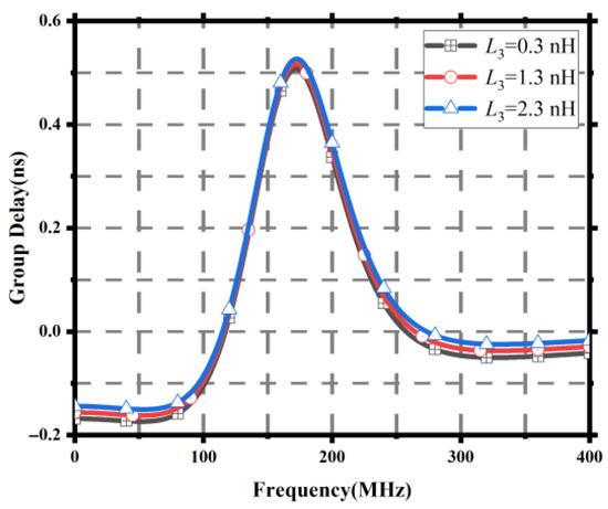
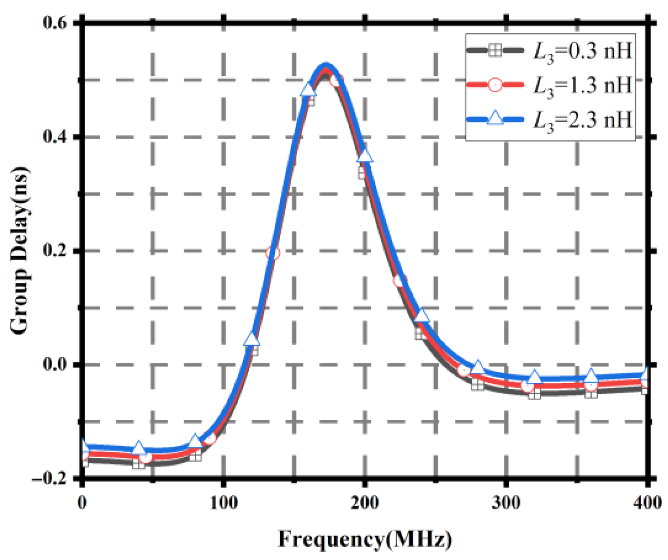
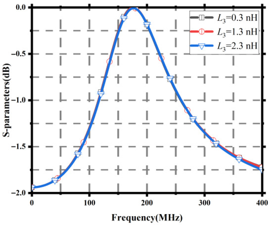
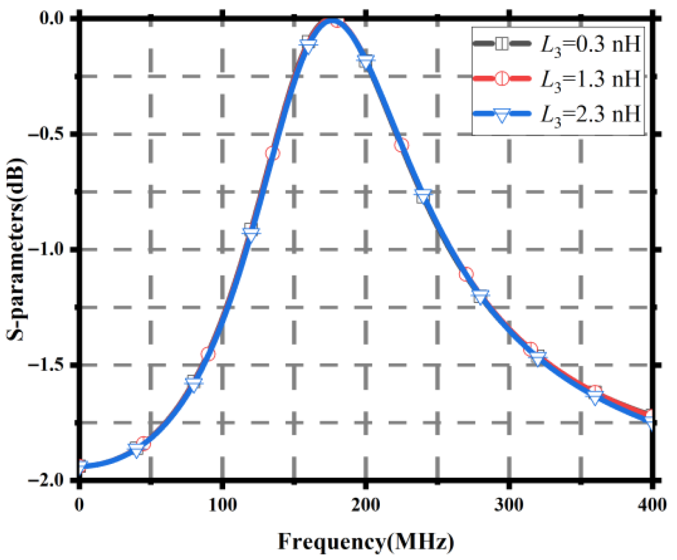
When the values of C1, R1, L1, R2, and L2 in the circuit remain unchanged, as shown in Table 8, and L3 is sequentially changed to 0.3 nH, 1.3 nH, and 2.3 nH, we observe the changes in the circuit transfer function and group delay. The circuit results in these three cases are shown in Table 13 and Figure 25 and Figure 26. Through observation, it is found that, as the value of inductance L3 increases, the group delay of the high-pass circuit at 0 MHz decreases. As the value of inductance L3 increases, the negative group delay also decreases. The degree of change in the circuit insertion loss is not significant, but, as the frequency increases, the insertion loss increases with the increase in inductance L3.
Table 13.
Circuit results with different 3 values.
Figure 25.
Group delay results for different 3 values.
Figure 26.
21 results for different 3 values.
3. Circuit Simulation with High-Pass and Low-Pass Negative Group Delay
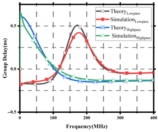
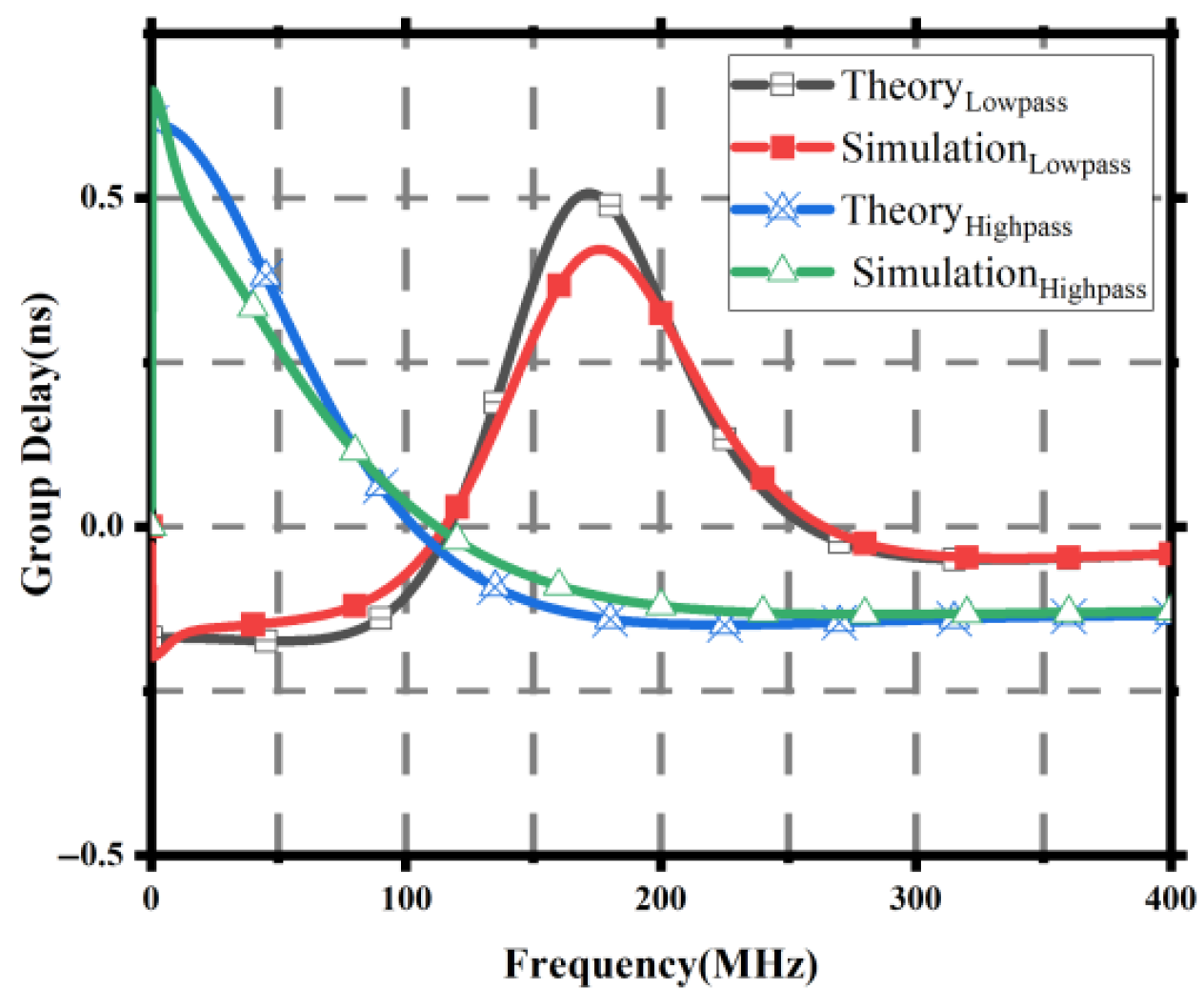
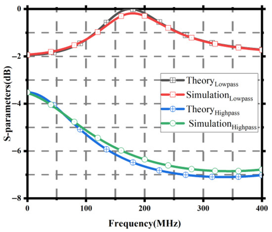
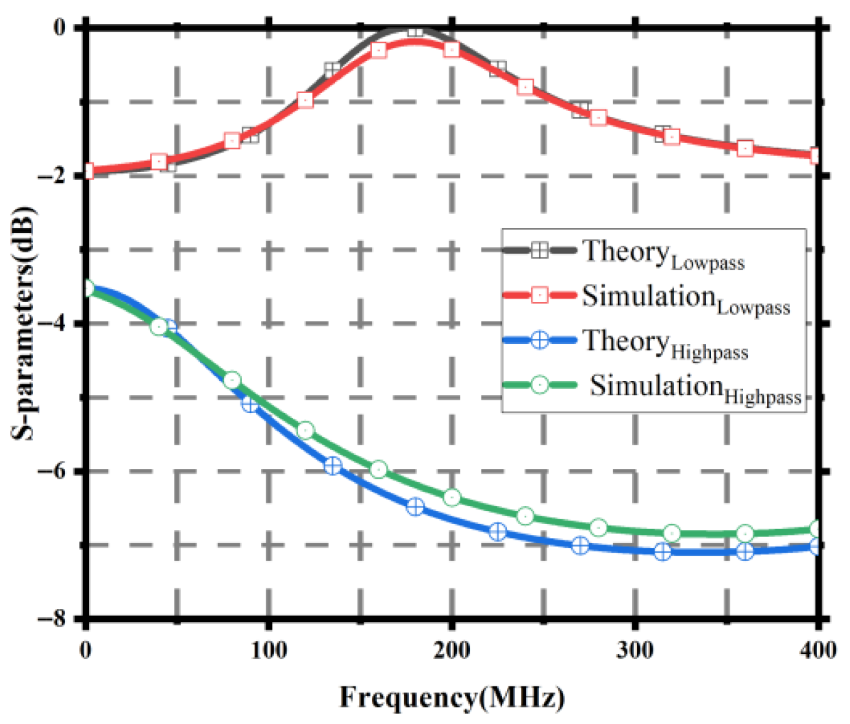
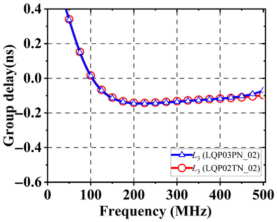
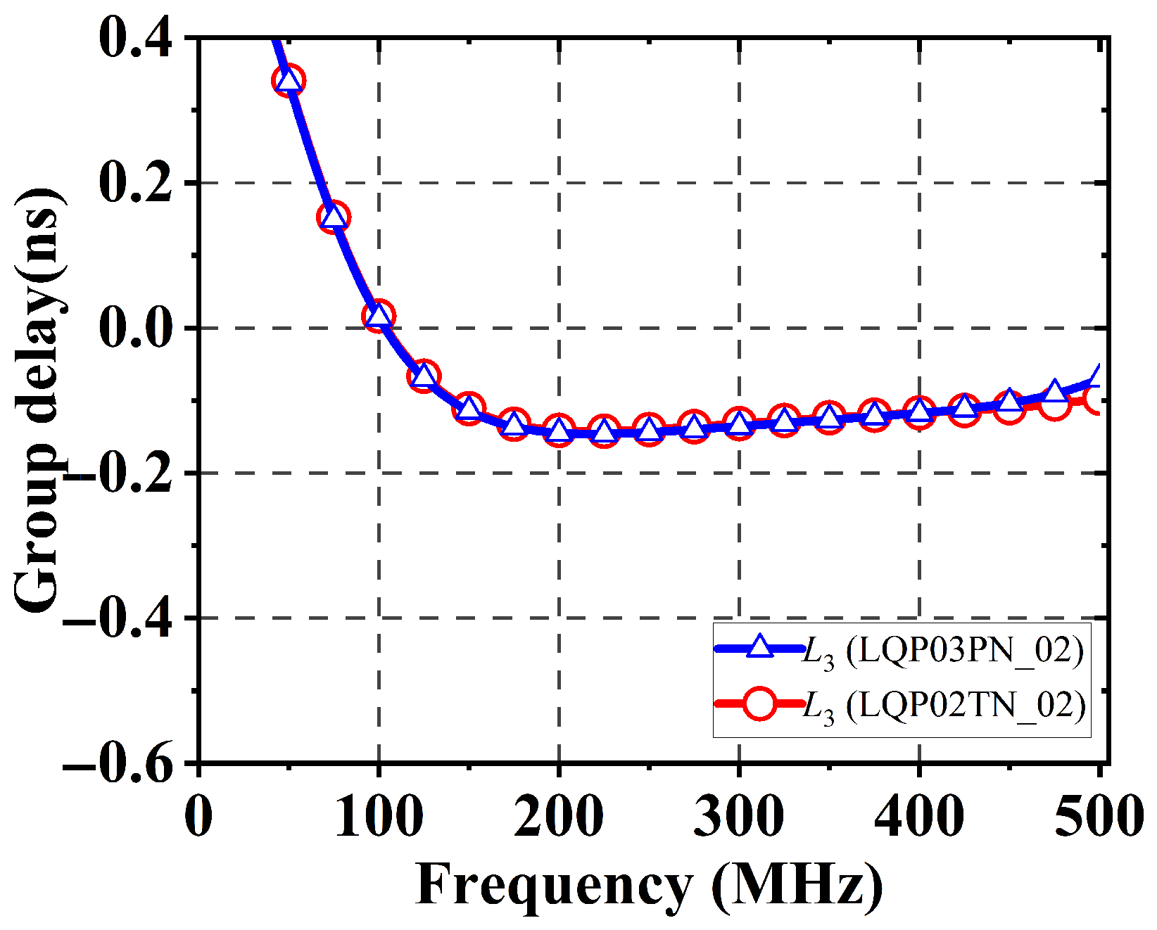
Based on the analysis of the circuit parameters, and considering the factors of the average negative group delay bandwidth and insertion loss, the parameters of the high-pass circuit are determined as in Table 14, and those of the low-pass circuit are as shown in Table 15. The circuit was simulated using the ADS software and Murata simulation library. The simulation results are shown in Table 14 and Table 15 and Figure 27 and Figure 28, and they are consistent with the theoretical results, indicating the feasibility of the experiment. We take inductor L3 as an example to analyze the effects of component tolerance on the circuit. We select inductors with different tolerances and the same inductance value in the Murata component library for simulation, and the simulation results are shown in Figure 29. The results obtained using inductors with different tolerances are essentially the same, which indicates that the component tolerances have a small effect on the circuit. As shown in Table 16, we achieve the characteristics of a larger negative group delay bandwidth, flatter bandwidth, and lower loss compared to other studies. During the comparison process, the GD ripple is calculated as shown in Equation (7).
Table 14.
High-pass circuit theory and simulation results.
Table 15.
Low-pass circuit theory and simulation results.
Figure 27.
Theoretical and simulation group delay results.
Figure 28.
Theoretical and simulation S21 results.
Figure 29.
Cluster delay results for 3 with different tolerances.
Table 16.
Comparison with other studies.
4. Conclusions
The proposed negative group delay circuit can achieve high- or low-pass negative group delay circuit functionalities through parameter adjustment, and it has multifunctionality. Moreover, the designed and implemented negative group delay circuit has the characteristics of a larger negative group delay bandwidth, better flatness, and lower transmission loss. Through testing, it has been proven to yield consistent experimental results and demonstrates feasibility. These results lay the foundation for subsequent research and can also be applied to various circuits to eliminate the originally generated positive group delay in the circuit and achieve the goal of reducing signal errors.
Author Contributions
Conceptualization, A.Y. and J.L.; methodology, A.Y.; validation, E.S., X.G. and N.C.; formal analysis, E.S.; investigation, E.S.; writing—original draft preparation, E.S.; writing—review and editing, A.Y. All authors have read and agreed to the published version of the manuscript.
Funding
This research received no external funding.
Institutional Review Board Statement
Not applicable.
Informed Consent Statement
Not applicable.
Data Availability Statement
The original contributions presented in this study are included in the article. Further inquiries can be directed to the corresponding author.
Conflicts of Interest
Author Junzheng Liu is from a company. The authors declare no conflicts of interest.
References
- Zhou, X.; Gu, T.C.; Wu, L.L.; Wan, F.Y.; Li, B.H.; Murad, N.; Lallechere, S.; Ravelo, B. S-matrix and bandpass negative group delay innovative theory of ti-geometrical shape microstrip structure. IEEE Access 2020, 8, 160363–160373. [Google Scholar] [CrossRef] [Scilit]
- Wan, F.Y.; Gu, T.C.; Ravelo, B.; Li, B.H.; Cheng, J.; Yuan, Q.Y. Negative group delay theory of a four-port RC-network feedback operational amplifier. IEEE Access 2019, 7, 75708–75720. [Google Scholar] [CrossRef] [Scilit]
- Yuan, A.X.; Fang, S.J.; Wang, Z.B.; Liu, H.M.; Zhang, H.J. A novel band-stop filter with band-pass, high-pass, and low-pass negative group delay characteristics. Int. J. Antennas Propag. 2021, 3207652. [Google Scholar] [CrossRef] [Scilit]
- Zhang, T.D.; Yang, T. A novel fully reconfigurable non foster capacitance using distributed negative group delay networks. IEEE Access 2019, 7, 92768–92777. [Google Scholar] [CrossRef] [Scilit]
- Ravelo, B.; Wan, F.Y.; Feng, J. All-Pass Negative Group Delay Function with Transmission Line Feedback Topology. IEEE Access 2019, 7, 155711–155723. [Google Scholar] [CrossRef] [Scilit]
- Ravelo, B.; Wan, F.Y.; Rahajandraibe, W.; Murad, N. Cable delay cancellation with low-pass NGD function. In Proceedings of the 2020 International Symposium on Electromagnetic Compatibility, EMC EUROPE, Rome, Italy, 23–25 September 2020; pp. 1–5. [Google Scholar]
- Wang, H.D.; Wu, Y.L.; Wu, Z.H.; Wang, W.M.; Liu, Y.N. Compact arbitrary terminated power divider with bandwidth-enhanced negative group delay characteristics. Int. J. Circ. Theor. Appl. 2019, 47, 909–916. [Google Scholar] [CrossRef] [Scilit]
- Ravelo, B.; Wu, L.; Wan, F.Y.; Rahajandraibe, W.; Murad, N. Negative group delay theory on Li topology. IEEE Access 2020, 8, 47596–47606. [Google Scholar] [CrossRef] [Scilit]
- Wu, Y.; Wang, H.; Zhuang, Z.; Liu, Y. Unidirectional reciprocal DC-block impedance transformer with flatness and broadband negative group delay characteristics. In Proceedings of the 2017 IEEE Electrical Design of Advanced Packaging and Systems Symposium (EDAPS), Haining, China, 14–16 December 2017; pp. 1–3. [Google Scholar]
- Wu, Y.; Wang, H.; Zhuang, Z.; Liu, Y.A.; Xue, Q.; Kishk, A.A. A novel arbitrary terminated unequal coupler with bandwidth-enhanced positive and negative group delay characteristics. IEEE Trans. Microw. Theory Tech. 2018, 66, 2170–2184. [Google Scholar] [CrossRef]
- Gomez-Garcia, R.; Munoz-Ferreras, J.; Feng, W.; Psychogiou, D. Input-reflectionless negative-group-delay bandstop-filter networks based on lossy complementary duplexers. In Proceedings of the 2019 IEEE MTT-S International Microwave Symposium (IMS), Boston, MA, USA, 2–7 June 2019; pp. 1031–1034. [Google Scholar]
- Wan, F.Y.; Wu, L.L.; Ravelo, B.; Ge, J. Analysis of interconnect line coupled with a radial-stub terminated negative group delay circuit. IEEE Trans. Electromagn. Compat. 2020, 62, 1813–1821. [Google Scholar] [CrossRef] [Scilit]
- Ravelo, B.; Wan, F.Y.; Lallechere, S.; Fontgalland, G.; Rahajandraibe, W. Design and test of crab-shaped negative group delay circuit. IEEE Des. Test 2022, 39, 67–76. [Google Scholar] [CrossRef] [Scilit]
- Wan, F.Y.; Li, N.D.; Ravelo, B.; Rahajandraibe, W.; Lalechere, S. Design of =|= shape stub-based negative group delay circuit. IEEE Des. Test 2021, 38, 78–88. [Google Scholar] [CrossRef] [Scilit]
- Chaudhary, G.; Jeong, Y. A design of power divider with negative group delay characteristics. IEEE Microw. Wirel. Compon. Lett. 2015, 25, 394–396. [Google Scholar] [CrossRef] [Scilit]
- Alomar, W.; Mortazawi, A. Method of generating negative group delay in phase arrays without using lossy circuits. In Proceedings of the 2013 IEEE International Wireless Symposium (IWS), Beijing, China, 14–18 April 2013; pp. 1–3. [Google Scholar]
- Wu, C.T.M.; Itoh, T. Maximally flat negative group-delay circuit: A microwave transversal filter approach. IEEE Trans. Microw. Theory Tech. 2014, 62, 1330–1342. [Google Scholar] [CrossRef] [Scilit]
- Wang, Z.B.; Meng, Y.W.; Fang, S.J.; Liu, H.M. Wideband flat negative group delay circuit with improved signal attenuation. IEEE Trans. Circuits Syst. II Express Briefs 2022, 8, 3371–3375. [Google Scholar] [CrossRef] [Scilit]
- Oh, S.S.; Shafai, L. Compensated circuit with characteristics of lossless double negative materials and its application to array antennas. IET Microw. Antenna Propag. 2007, 1, 29–38. [Google Scholar] [CrossRef] [Scilit]
- Kandic, M.; Bridges, G.E. Maximally Flat Negative Group Delay Prototype Filter Based on Capped Reciprocal Transfer Function of Classical Bessel Filter. Prog. Electromagn. Res. B 2025, 110, 91–105. [Google Scholar] [CrossRef] [Scilit]

Disclaimer/Publisher’s Note: The statements, opinions and data contained in all publications are solely those of the individual author(s) and contributor(s) and not of MDPI and/or the editor(s). MDPI and/or the editor(s) disclaim responsibility for any injury to people or property resulting from any ideas, methods, instructions or products referred to in the content. |
© 2025 by the authors. Licensee MDPI, Basel, Switzerland. This article is an open access article distributed under the terms and conditions of the Creative Commons Attribution (CC BY) license (https://creativecommons.org/licenses/by/4.0/).