
On Standard Cell-Based Design for Dynamic Voltage Comparators and Relaxation Oscillators


Abstract
1. Introduction
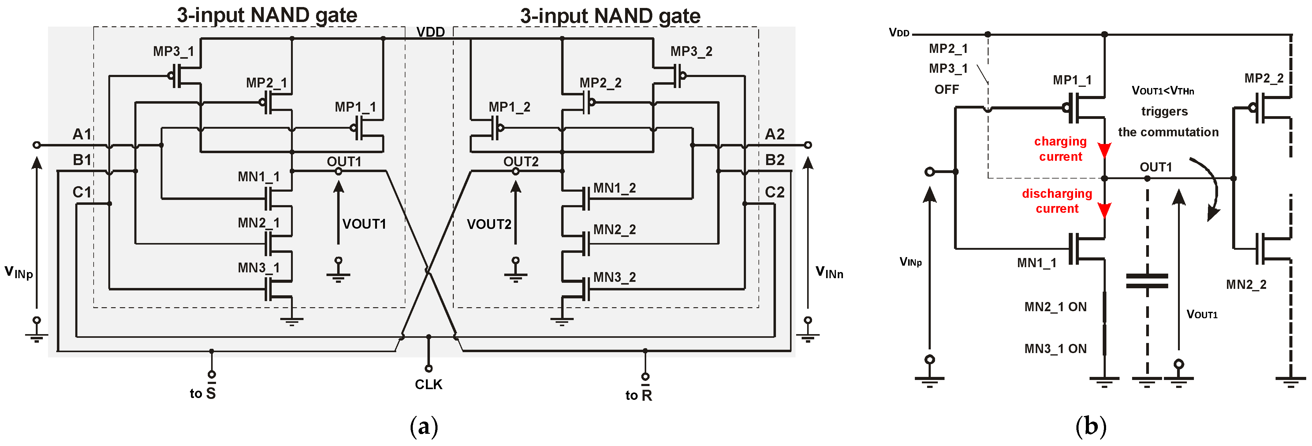
2. Fully Synthesizable Rail-to-Rail Dynamic Voltage Comparator
3. Digital-Gate Design: From Dynamic Voltage Comparators to Relaxation Oscillators
4. A Wake-Up Relaxation Oscillator Made with DLS Gates
5. Conclusions
Funding
Institutional Review Board Statement
Informed Consent Statement
Data Availability Statement
Conflicts of Interest
References
- Aiello, O. Ultra-Low-Power ICs for the Internet of Things. J. Low Power Electron. Appl. 2023, 13, 38. [Google Scholar] [CrossRef]
- Aiello, O.; Crovetti, P.; Alioto, M. Ultra-Low Power and Minimal Design Effort Interfaces for the Internet of Things: Invited paper. In Proceedings of the 2019 IEEE International Circuits and Systems Symposium (ICSyS), Kuantan, Malaysia, 18–19 September 2019; pp. 1–4. [Google Scholar]
- Aiello, O.; Crovetti, P.; Alioto, M. Minimum-Effort Design of Ultra-Low Power Interfaces for the Internet of Things. In Proceedings of the 2019 26th IEEE International Conference on Electronics, Circuits and Systems (ICECS), Genoa, Italy, 27–29 November 2019; pp. 105–106. [Google Scholar]
- Di Patrizio Stanchieri, G.; Aiello, O.; De Marcellis, A. A 0.4 V 180 nm CMOS Sub-μW Ultra-Compact and Low-Effort Design PWM-Based ADC. In Proceedings of the IEEE International Symposium on Circuits and Systems (ISCAS), Singapore, 19–22 May 2024; pp. 1–5. [Google Scholar] [CrossRef]
- Stanchieri, G.D.P.; De Marcellis, A.; Faccio, M.; Palange, E.; Aiello, O. A Fully Integrated CMOS 0.3 V 335 nW PWM-Based Light-to-Digital Converter for Optoelectronic Sensing Systems in Biomedical Applications. IEEE Sens. Lett. 2025, 9, 3500404. [Google Scholar] [CrossRef]
- Stanchieri, G.D.P.; Aiello, O.; De Marcellis, A. A reduced effort design, low power, extremely compact, CMOS ADC based on voltage-to-time converter. AEU Int. J. Electron. Commun. 2025, 196, 155790. [Google Scholar] [CrossRef]
- Rodovalho, L.-H.; Aiello, O. Inverter-Based Amplifier with Active Frequency Compensation and Adaptive Voltage Scaling. In Proceedings of the IEEE International Symposium on Circuits and Systems (ISCAS), Singapore, 19–22 May 2024; pp. 1–5. [Google Scholar] [CrossRef]
- Catania, A.; Benvenuti, L.; Ria, A.; Manfredini, G.; Piotto, M.; Bruschi, P. A 2 nW 0.25 V 140 dB-FOM Inverter-Based First Order ΔΣ Modulator. IEEE Trans. Circuits Syst. II Express Briefs 2020, 67, 1514–1518. [Google Scholar]
- Della Sala, R.; Centurelli, F.; Scotti, G.; Palumbo, G. Standard-Cell-Based Comparators for Ultra-Low Voltage Applications: Analysis and Comparisons. Chips 2023, 2, 173–194. [Google Scholar] [CrossRef]
- Weaver, S.; Hershberg, B.; Kurahashi, P.; Knierim, D.; Moon, U.-K. Stochastic flash analog-to-digital conversion. IEEE Trans. Circuits Syst. I Reg. Papers 2010, 57, 2825–2833. [Google Scholar] [CrossRef]
- Weaver, S.; Hershberg, B.; Moon, U.-K. Digitally synthesized stochastic flash ADC using only standard digital cells. IEEE Trans. Circuits Syst. I Reg. Papers 2014, 61, 84–91. [Google Scholar] [CrossRef]
- Fahmy, A.; Liu, J.; Kim, T.; Maghari, N. An All-Digital Scalable and Reconfigurable Wide-Input Range Stochastic ADC Using Only Standard Cells. IEEE Trans. Circuits Syst. II Express Briefs 2015, 62, 731–735. [Google Scholar] [CrossRef]
- Liu, J.; Maghari, N. A fully-synthesizable 0.6V digital LDO with dual-loop control using digital standard cells. In Proceedings of the 2016 14th IEEE International New Circuits and Systems Conference (NEWCAS), Vancouver, BC, Canada, 26–29 June 2016; pp. 1–4. [Google Scholar] [CrossRef]
- Liu, J.; Park, B.; Guzman, M.; Fahmy, A.; Kim, T.; Maghari, M. A Fully Synthesized 77-dB SFDR Reprogrammable SRMC Filter Using Digital Standard Cells. IEEE Trans. VLSI Syst. 2018, 26, 1126–1138. [Google Scholar] [CrossRef]
- Aiello, O.; Crovetti, P.; Alioto, M. Fully synthesizable rail-to-rail dynamic voltage comparator for operation down to 0.3 V. In Proceedings of the 2018 IEEE International Symposium on Circuits and Systems (ISCAS), Florence, Italy, 27–30 May 2018; pp. 1–5. [Google Scholar]
- Aiello, O.; Crovetti, P.; Toledo, P.; Alioto, M. Rail-to-Rail Dynamic Voltage Comparator Scalable down to pW-Range Power and 0.15-V Supply. IEEE Trans. Circuits Syst. II Express Briefs 2021, 68, 2675–2679. [Google Scholar] [CrossRef]
- Aiello, O.; Pedro Toledo, P. Temperature Characterization of a Fully-synthesizable Rail-to-Rail Dynamic Voltage Comparator operating down to 0.15-V: (Invited paper). In Proceedings of the 2021 19th IEEE International New Circuits and Systems Conference (NEWCAS), Toulon, France, 13–16 June 2021; pp. 1–4. [Google Scholar]
- Bui, D.-H.; Tran, D.-M.; Caviglia, D.D.; Aiello, O. Fully Synthesizable Dynamic Voltage Comparator across technology nodes and scaled supply voltages. In Proceedings of the IEEE International Symposium on Circuits and Systems (ISCAS), Singapore, 19–22 May 2024; pp. 1–5. [Google Scholar] [CrossRef]
- Manno, A.; Scotti, G.; Palumbo, G. Design of Ultra-Low-Power Rail-to-Rail Input Common Mode Range Standard-Cell-Based Comparators. J. Low Power Electron. Appl. 2025, 15, 14. [Google Scholar] [CrossRef]
- Li, X.; Zhou, T.; Ji, Y.; Li, Y. A 0.35 V-to-1.0 v. synthesizable rail-to-rail dynamic voltage comparator based OAI&AOI logic. Analog Integr. Circuits Signal Process. 2020, 104, 351–357. [Google Scholar]
- Li, M.; Wang, J.; Cheng, X.; Han, J.; Zeng, X. A Digital Synthesizable Full Common-mode Input Range Dynamic Voltage Comparator. In Proceedings of the 2020 IEEE 15th International Conference on Solid-State & Integrated Circuit Technology (ICSICT), Kunming, China, 3–6 November 2020; pp. 1–3. [Google Scholar] [CrossRef]
- Zou, X.; Nakatake, S. A Fully Synthesizable, 0.3V, 10nW Rail-to-rail Dynamic Voltage Comparator. In Proceedings of the 2020 IEEE 63rd International Midwest Symposium on Circuits and Systems (MWSCAS), Springfield, MA, USA, 9–12 August 2020; pp. 199–202. [Google Scholar] [CrossRef]
- Zhou, T.; Li, X.; Ji, Y.; Li, Y. A 0.25–1.0 v. fully synthesizable three-stage dynamic voltage comparator based XOR&XNOR&NAND&NOR logic. Analog Integr. Circuits Signal Process. 2021, 108, 221–228. [Google Scholar]
- Sasidhar, R.S.; Umamaheswara, R.G. A Novel Low Power Digital-Based Analog Voltage Comparator Circuit. In Proceedings of the 2022 6th International Conference on Computation System and Information Technology for Sustainable Solutions (CSITSS), Bangalore, India, 21–23 December 2022; pp. 1–6. [Google Scholar]
- Della Sala, R.; Bocciarelli, C.; Centurelli, F.; Spinogatti, V.; Trifiletti, A. A Novel Ultra-Low Voltage Fully Synthesizable Comparator exploiting NAND Gates. In Proceedings of the 2023 18th Conference on Ph.D Research in Microelectronics and Electronics (PRIME), Valencia, Spain, 18–21 June 2023; pp. 21–24. [Google Scholar]
- Wang, S.; Guo, Y.; Pan, Q.; Liu, X.; Wang, S.; Jin, J. A Fully Synthesizable Dynamic Voltage Comparator with Time-Domain Offset Calibration. In Proceedings of the 2023 IEEE 66th International Midwest Symposium on Circuits and Systems (MWSCAS), Tempe, AZ, USA, 6–9 August 2023; pp. 482–485. [Google Scholar] [CrossRef]
- Della Sala, R.; Centurelli, F.; Scotti, G.; Palumbo, G. Rail to Rail ICMR and High Performance ULV Standard-Cell-Based Comparator for Biomedical and IoT Applications. IEEE Access 2024, 12, 4642–4659. [Google Scholar] [CrossRef]
- Aiello, O.; Crovetti, P.; Alioto, M. A Sub-Leakage PW-Power HZ-Range Relaxation Oscillator Operating with 0.3V-1.8V Unregulated Supply. In Proceedings of the 2018 IEEE Symposium on VLSI Circuits, Honolulu, HI, USA, 18–22 June 2018; pp. 119–120. [Google Scholar] [CrossRef]
- Aiello, O.; Crovetti, P.; Lin, L.; Alioto, M. A pW-Power Hz-Range Oscillator Operating with a 0.3V–1.8V Unregulated Supply. IEEE J. Solid-State Circuits 2019, 54, 1487–1496. [Google Scholar] [CrossRef]
- Aiello, O.; Crovetti, P.; Alioto, M. Wake-Up Oscillators with pW Power Consumption in Dynamic Leakage Suppression Logic. In Proceedings of the 2019 IEEE International Symposium on Circuits and Systems (ISCAS), Sapporo, Japan, 26–29 May 2019; pp. 1–5. [Google Scholar] [CrossRef]
- Pelgrom, M.J.M.; Duinmaijer, C.J.; Welbers, A.P.G. Matching properties of MOS transistors. IEEE J. Solid-State Circuits 1989, 24, 1433–1440. [Google Scholar] [CrossRef]
- Seo, M.J.; Roh, Y.J.; Chang, D.J.; Kim, W.; Kim, Y.D.; Ryu, S.T. A reusable code-based SAR ADC design with CDAC compiler and synthesizable analog building blocks. IEEE Trans. Circuits Syst. II Exp. Briefs 2018, 65, 1904–1908. [Google Scholar] [CrossRef]
- Ojima, N.; Xu, Z.; Iizuka, T. A 0.0053-mm2 6-bit fully-standard-cell-based synthesizable SAR ADC in 65 nm CMOS. In Proceedings of the 2019 17th IEEE International New Circuits and Systems Conference (NEWCAS), Munich, Germany, 23–26 June 2019; pp. 1–4. [Google Scholar]
- Park, J.-E.; Hwang, Y.-H.; Jeong, D.-K. A 0.5-V fully synthesizable SAR ADC for on-chip distributed waveform monitors. IEEE Access 2019, 7, 63686–63697. [Google Scholar] [CrossRef]
- Xu, Z.; Ojima, N.; Li, S.; Iizuka, T. An all-standard-cell-based synthesizable SAR ADC with nonlinearity-compensated RDAC. IEEE Trans. VLSI Syst. 2021, 29, 2153–2162. [Google Scholar] [CrossRef]
- Yang, F.; Bui, D.H.; Zhao, Y.; Qi, L.; Zhang, J.; Tran, X.T.; Li, Y. Understanding Synthesizable Design Methodologies for Mixed-Signal SAR ADC Circuits. Integr. Circuits Syst. 2024, 1, 120–126. [Google Scholar] [CrossRef]
- Lim, W.; Lee, I.; Sylvester, D.; Blaauw, D. Batteryless sub-nW Cortex-M0+ processor with dynamic leakage-suppression logic. In Proceedings of the 2015 IEEE International Solid-State Circuits Conference—(ISSCC) Digest of Technical Papers, San Francisco, CA, USA, 22–26 February 2015; pp. 1–3. [Google Scholar]
- Bol, D.; Ambroise, R.; Flandre, D.; Legat, J.-D. Building Ultra-Low-Power Low-Frequency Digital Circuits with High-Speed Devices. In Proceedings of the 2007 14th IEEE International Conference on Electronics, Circuits and Systems, Marrakech, Morocco, 11–14 December 2007; pp. 1404–1407. [Google Scholar]
- Yin, J.; Stan, M.R. Design and Modeling for Very High-sensitivity UHF RF Energy Harvesting Circuit. In Proceedings of the 2025 IEEE 16th Latin America Symposium on Circuits and Systems (LASCAS), Bento Gonçalves, Brazil, 25–28 February 2025; pp. 1–5. [Google Scholar] [CrossRef]
- Shavit, N.; Stanger, I.; Taco, R.; Yavits, L.; Fish, A. Low Power, Energy Efficient and High Performance Triple Mode Logic for IoT Applications. In Proceedings of the 2024 19th Conference on Ph.D Research in Microelectronics and Electronics (PRIME), Larnaca, Cyprus, 9–12 June 2024; pp. 1–4. [Google Scholar] [CrossRef]
- Yin, J.; Stan, M.R. A Low Power SRAM with Fully Dynamic Leakage Suppression for IoT Nodes. In Proceedings of the 2023 24th International Symposium on Quality Electronic Design (ISQED), San Francisco, CA, USA, 5–7 April 2023; pp. 1–8. [Google Scholar] [CrossRef]
- Chen, X.; Chen, G.; Yu, X.; Wang, Y.; Niitsu, K. A 52.3% Peak Efficiency 22nm CMOS Low-Power Light-Adaptive Self-Oscillating Voltage Doubler Using Scalable Dynamic Leakage-Suppression Logic. In Proceedings of the 2022 IEEE 13th Latin America Symposium on Circuits and System (LASCAS), Puerto Varas, Chile, 1–4 March 2022; pp. 1–4. [Google Scholar] [CrossRef]
- Wang, Y.; Chen, G.; Yu, X.; Chen, X.; Niitsu, K. A 22nm CMOS 0.2V 13.3nW 16T SRAM Using Dynamic Leakage Suppression and Half-Selected Free Technique. In Proceedings of the 2021 IEEE Asia Pacific Conference on Circuit and Systems (APCCAS), Penang, Malaysia, 22–26 November 2021; pp. 29–32. [Google Scholar] [CrossRef]
- Tan, J.S.Y.; Park, J.H.; Li, J.; Dong, Y.; Chan, K.H.; Ho, G.W.; Yoo, J. A Fully Energy-Autonomous Temperature-to-Time Converter Powered by a Triboelectric Energy Harvester for Biomedical Applications. IEEE J. Solid-State Circuits 2021, 56, 2913–2923. [Google Scholar] [CrossRef]
- Truesdell, D.S.; Calhoun, B.H. A Single-Supply 6-Transistor Voltage Level Converter Design Reaching 8.18-fJ/Transition at 0.3–1.2-V Range or 44-fW Leakage at 0.8–2.5-V Range. IEEE Solid-State Circuits Lett. 2020, 3, 502–505. [Google Scholar] [CrossRef]
- Tan, J.S.Y.; Park, J.; Li, J.; Dong, Y.; Chan, K.H.; Ho, G.W.; Yoo, J. A 0.14 pJ/conversion Fully Energy-Autonomous Temperature-to-Time Converter for Biomedical Applications. IEEE Solid-State Circuits Lett. 2020, 3, 466–469. [Google Scholar] [CrossRef]
- Cañada, J.; Yoshida, Y.; Miura, H.; Nakano, N. An On-Chip Ultra-Low-Power Hz-Range Ring Oscillator Based on Dynamic Leakage Suppression Logic. In Proceedings of the 2020 35th International Technical Conference on Circuits/Systems, Computers and Communications (ITC-CSCC), Nagoya, Japan, 3–6 July 2020; pp. 378–383. [Google Scholar]
- Truesdell, D.S.; Calhoun, B.H. Improving Dynamic Leakage Suppression Logic with Forward Body Bias in 65nm CMOS. In Proceedings of the 2019 IEEE SOI-3D-Subthreshold Microelectronics Technology Unified Conference (S3S), San Jose, CA, USA, 14–17 October 2019; pp. 1–2. [Google Scholar] [CrossRef]
- Kobayashi, A.; Hayashi, K.; Arata, S.; Murakami, S.; Xu, G.; Islam, Z.; Niitsu, K. A 2.1-nW Burst-Pulse-Counting Supply Voltage Monitor for Biofuel-Cell-Combined Biosensing Systems in 180-nm CMOS. In Proceedings of the 2019 IEEE Biomedical Circuits and Systems Conference (BioCAS), Nara, Japan, 17–19 October 2019; pp. 1–4. [Google Scholar] [CrossRef]
- Kawaguchi, H.; Nose, K.; Sakurai, T. A super cut-off CMOS (SCCMOS) scheme for 0.5-V supply voltage with picoampere stand-by current. IEEE J. Solid-State Circuits 2000, 35, 1498–1501. [Google Scholar] [CrossRef]
- Liu, X.; Sanchez-Sinencio, E. A 0.45-to-3V reconfigurable charge pump energy harvester with two-dimensional MPPT for Internet of Things. In Proceedings of the 2015 IEEE International Solid-State Circuits Conference—(ISSCC) Digest of Technical Papers, San Francisco, CA, USA, 22–26 February 2015; pp. 1–3. [Google Scholar]
- LTC3107 Ultralow Voltage Energy Harvester and Primary Battery Life Extender, Linear Technologies Corp. 2013. Available online: https://www.analog.com/media/en/technical-documentation/data-sheets/3107f.pdf (accessed on 1 July 2025).
- Savanth, A.; Weddell, A.S.; Myers, J.; Flynn, D.; Al-Hashimi, B.M. A Sub-nW/kHz Relaxation Oscillator with Ratioed Reference and Sub-Clock Power Gated Comparator. IEEE J. Solid-State Circuits 2019, 54, 3097–3106. [Google Scholar] [CrossRef]
- Liu, Y.; Zhu, Z.; Bao, R.; Lin, J.; Yin, J.; Li, Q.; Mak, P.-I.; Yang, S. A Compact Sub-nW/kHz Relaxation Oscillator Using a Negative-Offset Comparator with Chopping and Piecewise Charge-Acceleration in 28-nm CMOS. IEEE Trans. Circuits Syst. I Regul. Pap. 2023, 71, 515–525. [Google Scholar] [CrossRef]
- Zhao, G.; Xiao, Z.; Mak, P.-I.; Martins, R.P.; Law, M.-K. One-Cycle-Startup Relaxation Oscillator Using Ratiometric Threshold-Referenced and Self-Synchronized Power Gating Techniques. IEEE Trans. Circuits Syst. II Express Briefs 2023, 71, 56–60. [Google Scholar] [CrossRef]
- Mirchandani, N.; Shrivastava, A. A 254-nW 20-kHz On-Chip RC Oscillator with 21-ppm/°C Minimum Temperature Stability and 10-ppm Long Term Stability. IEEE Trans. Circuits Syst. I Regul. Pap. 2023, 70, 2823–2833. [Google Scholar] [CrossRef]
- Wei, Y.; Yang, S.; Liu, Y.; Bao, R.; Zhu, Z.; Lin, J.; Zhang, Z.; Chen, Y.; Yin, J.; Mak, P.-I.; et al. A 0.0043-mm2 0.085-μW/MHz Relaxation Oscillator Using Charge-Prestored Asymmetric Swings R-RC Network. IEEE Trans. Very Large Scale Integr. (VLSI) Syst. 2023, 31, 1248–1252. [Google Scholar] [CrossRef]
- Loo, M.H.-W.; Ramiah, H.; Lei, K.-M.; Lim, C.C.; Lai, N.S.; Mak, P.-I.; Martins, R.P. Fully-Integrated Timers for Ultra-Low-Power Internet-of-Things Nodes—Fundamentals and Design Techniques. IEEE Access 2022, 10, 65936–65950. [Google Scholar] [CrossRef]
- Wang, Z.; Liu, Y.; Zhou, P.; Tan, Z.; Fan, H.; Zhang, Y.; Shen, L.; Ru, J.; Wang, Y.; Ye, L.; et al. A 148-nW Reconfigurable Event-Driven Intelligent Wake-Up System for AIoT Nodes Using an Asynchronous Pulse-Based Feature Extractor and a Convolutional Neural Network. IEEE J. Solid-State Circuits 2021, 56, 3274–3288. [Google Scholar] [CrossRef]
- Lei, K.M.; Mak, P.I.; Martins, R.P. A 0.35-V 5200-μm2 2.1-MHz Temperature-Resilient Relaxation Oscillator with 667 fJ/Cycle Energy Efficiency Using an Asymmetric Swing-Boosted RC Network and a Dual-Path Comparator. IEEE J. Solid-State Circuits 2021, 56, 2701–2710. [Google Scholar] [CrossRef]
- Truesdell, D.S.; Li, S.; Calhoun, B.H. A 0.5-V 560-kHz 18.8-fJ/Cycle On-Chip Oscillator with 96.1-ppm/°C Steady-State Stability Using a Duty-Cycled Digital Frequency-Locked Loop. IEEE J. Solid-State Circuits 2021, 56, 1241–1253. [Google Scholar] [CrossRef]
- Zhou, R.; Wang, L.; Yang, J.; Li, Z.; Zhao, X.; Liu, S. A 8.1-nW, 4.22-kHz, −40–85 °C relaxation oscillator with subthreshold leakage current compensation and forward body bias buffer for low power IoT applications. Microelectron. J. 2024, 144, 106090. [Google Scholar] [CrossRef]
- Lei, K.M.; Mak, P.I.; Martins, R.P. Martins, Ultra-Low-Voltage Clock References, Analog and Mixed-Signal Circuits in Nanoscale CMOS. In Analog Circuits and Signal Processing; Springer: Berlin/Heidelberg, Germany, 2023; p. 91. [Google Scholar]
- Li, Z.; Zhao, H.; Liu, J.; Qiao, S.; Zhou, Y. A current-capacitor-based voltage average feedback RC oscillator with no comparators. AEU Int. J. Electron. Commun. 2023, 167, 154672. [Google Scholar] [CrossRef]
- Liao, Y.; Chan, P.K. A 1.1 V 25 ppm/°C Relaxation Oscillator with 0.045%/V Line Sensitivity for Low Power Applications. J. Low Power Electron. Appl. 2023, 13, 15. [Google Scholar] [CrossRef]
- Hu, Y.; Li, Z.; Hou, J.; Ma, W.; Lu, C.; Xiao, Z.; Liu, H.; Hu, W. A constant charging-current relaxation oscillator with a duty-cycled main comparator and an adaptive auxiliary comparator. Microelectron. J. 2022, 128, 105566. [Google Scholar] [CrossRef]
- Li, Z.; Zhao, H.; Yin, J.; Qiao, S.; Zhou, Y. A fully integrated RC oscillator with adaptive-body-biasing. IEICE Electron. Express 2022, 19, 20220102. [Google Scholar] [CrossRef]
- Lim, J.; Jang, T.; Saligane, M.; Yasuda, M.; Miyoshi, S.; Kawaminami, M.; Blaauw, D.; Sylvester, D. A 224 pW 260 ppm/°C Gate-Leakage-based Timer for Ultra-Low Power Sensor Nodes with Second-Order Temperature Dependency Cancellation. In Proceedings of the 2018 IEEE Symposium on VLSI Circuits, Honolulu, HI, USA, 18–22 June 2018. [Google Scholar]
- Wang, H.; Mercier, P.P. A 1.6%/V 124.2 pW 9.3 Hz Relaxation Oscillator Featuring a 49.7 pW Voltage and Current Reference Generator. In Proceedings of the ESSCIRC 2017—43rd IEEE European Solid State Circuits Conference, Leuven, Belgium, 11–14 September 2017; pp. 99–102. [Google Scholar]
- Wang, H.; Mercier, P.P. A Reference-Free Capacitive-Discharging Oscillator Architecture Consuming 44.4 pW/75.6 nW at 2.8 Hz/6.4 kHz. IEEE J. Solid-State Circuits 2016, 51, 1423–1435. [Google Scholar] [CrossRef]
- Nadeau, P.M.; Paidimarri, A.; Chandrakasan, A.P. Ultra Low-Energy Relaxation Oscillator with 230 fJ/cycle Efficiency. IEEE J. Solid-State Circuits 2016, 51, 789–799. [Google Scholar] [CrossRef]
- Jeong, S.; Lee, I.; Blaauw, D.; Sylvester, D. A 5.8 nW CMOS Wake-Up Timer for Ultra-Low-Power Wireless Applications. IEEE J. Solid-State Circuits 2015, 50, 1754–1763. [Google Scholar] [CrossRef]
- Aiello, O.; Crovetti, P.; Alioto, M. Conversion Time-Power Tradeoff in Capacitance-to-Digital Converters with Dual-Mode Logic. In Proceedings of the 2022 35th SBC/SBMicro/IEEE/ACM Symposium on Integrated Circuits and Systems Design (SBCCI), Porto Alegre, Brazil, 22–26 August 2022; pp. 1–5. [Google Scholar]
- Aiello, O.; Crovetti, P. Capacitance-to-digital converter in dual-mode logic: Power consumption vs conversion time trade-off. Analog. Integr. Circuits Signal Process. 2023, 117, 35–44. [Google Scholar] [CrossRef]
- Lin, L.; Jain, S.; Alioto, M. Sub-nW Microcontroller With Dual-Mode Logic and Self-Startup for Battery-Indifferent Sensor Nodes. IEEE J. Solid-State Circuits 2020, 56, 1618–1629. [Google Scholar] [CrossRef]
- Aiello, O.; Crovetti, P.; Alioto, M. 5.2 Capacitance-to-Digital Converter for Operation Under Uncertain Harvested Voltage down to 0.3V with No Trimming, Reference and Voltage Regulation. In Proceedings of the 2021 IEEE International Solid-State Circuits Conference (ISSCC), San Francisco, CA, USA, 13–22 February 2021; pp. 74–76. [Google Scholar] [CrossRef]
- Aiello, O.; Crovetti, P.S.; Alioto, M. Capacitance-to-Digital Converter for Harvested Systems Down to 0.3 V with No Trimming, Reference, and Voltage Regulation. IEEE Trans. Circuits Syst. I Regul. Pap. 2023, 70, 1439–1449. [Google Scholar] [CrossRef]
- Aiello, O.; Alioto, M. Capacitance-Based Voltage Regulation- and Reference-Free Temperature-to-Digital Converter down to 0.3 V and 2.5 nW for Direct Harvesting. In Proceedings of the ESSCIRC 2022—IEEE 48th European Solid State Circuits Conference (ESSCIRC), Milan, Italy, 19–22 September 2022; pp. 381–384. [Google Scholar] [CrossRef]


Disclaimer/Publisher’s Note: The statements, opinions and data contained in all publications are solely those of the individual author(s) and contributor(s) and not of MDPI and/or the editor(s). MDPI and/or the editor(s) disclaim responsibility for any injury to people or property resulting from any ideas, methods, instructions or products referred to in the content. |
© 2025 by the author. Licensee MDPI, Basel, Switzerland. This article is an open access article distributed under the terms and conditions of the Creative Commons Attribution (CC BY) license (https://creativecommons.org/licenses/by/4.0/).
Share and Cite
Aiello, O. On Standard Cell-Based Design for Dynamic Voltage Comparators and Relaxation Oscillators. Chips 2025, 4, 31. https://doi.org/10.3390/chips4030031
Aiello O. On Standard Cell-Based Design for Dynamic Voltage Comparators and Relaxation Oscillators. Chips. 2025; 4(3):31. https://doi.org/10.3390/chips4030031
Chicago/Turabian StyleAiello, Orazio. 2025. "On Standard Cell-Based Design for Dynamic Voltage Comparators and Relaxation Oscillators" Chips 4, no. 3: 31. https://doi.org/10.3390/chips4030031
APA StyleAiello, O. (2025). On Standard Cell-Based Design for Dynamic Voltage Comparators and Relaxation Oscillators. Chips, 4(3), 31. https://doi.org/10.3390/chips4030031