


Abstract
The κ-phase gallium oxide (κ-Ga2O3) has emerged as a promising material for next-generation electronic devices owing to its ultra-wide band gap, remarkable spontaneous polarization and unique ferroelectricity. We have investigated the two-dimensional electron gas (2DEG) characteristics and device performance of κ-Ga2O3/GaN HEMTs via numerical simulations. The κ-Ga2O3/GaN heterostructure exhibits a significantly enhanced 2DEG density (~1.05 × 1014 cm−2), which is nearly an order of magnitude higher than that of conventional AlGaN/GaN HEMTs, due to the strong polarization effect. For a barrier thickness of 25 nm, the κ-Ga2O3/GaN HEMT exhibits a maximum drain current density (ID,max) of 4.40 A/mm at VGS = 2 V and a peak transconductance (gm,max) of 0.45 S/mm, accompanied by a steep subthreshold swing (SS) of 63.2 mV/decade. Furthermore, we find that the absolute value of threshold voltage increases with the barrier thickness and the peak transconductance decreases with the increase in barrier thickness. When the thickness reaches 40 nm, the 2DEG density becomes saturated with a value of 1.12 × 1014 cm−2. Moreover, by incorporating a p-type GaN cap layer into the κ-Ga2O3/GaN heterostructure, a normally off operation is achieved, with a positive threshold voltage as the acceptor concentration exceeds 8.0 × 1017 cm−3. These results highlight the potential of κ-Ga2O3/GaN heterostructures for high-performance power electronic applications.
1. Introduction
High-electron-mobility transistors (HEMTs) based on GaN are key devices for achieving high-power and high-frequency performance in applications such as power regulation, radar systems, and microwave transmitters [1,2,3]. These devices are highly favored due to their high current density, large power output, and fast switching speed, particularly under high electric field and high-temperature operating conditions. These superior characteristics originate from the polarization-induced two-dimensional electron gas (2DEG), which has a high carrier density (~1 × 1013 cm−2) and high mobility (~2000 cm2 V−1 s−1) at room temperature [4,5]. Further boosting the 2DEG density at the heterointerface is critically essential to enhance the output performance of HEMTs.
Ultra-wide bandgap semiconductor, Ga2O3, has emerged as a research hotspot for next-generation power electronics. Notably, κ-Ga2O3, owing to its non-centrosymmetric orthorhombic crystal structure, exhibits a high spontaneous polarization. The theoretical spontaneous polarization coefficient reaches up to 23 μC/cm2, exceeding those of III-nitride semiconductors such as AlN (−8.1 μC/cm2) and GaN (−2.9 μC/cm2) [6,7]. Heterostructures based on κ-Ga2O3 can support extremely high-density 2DEG [8,9,10]. In addition, κ-Ga2O3 possesses a high dielectric constant [7] and unique ferroelectric properties [6,8]. These features introduce an additional degree of freedom for realizing the high density of 2DEG [11,12]. The growth of κ-Ga2O3 on GaN and other III-nitride semiconductors has been demonstrated to be feasible [13,14,15,16,17,18]. Facilitated by high elastic strain, high-quality κ-Ga2O3 thin films can be achieved on lattice-mismatched substrates such as sapphire, GaN, AlN, and SiC using techniques including halide vapor phase epitaxy (HVPE), mist chemical vapor deposition (mist-CVD), and metal–organic chemical vapor deposition (MOCVD) [13,19,20,21,22,23,24,25,26]. These suggest the potential for the design and fabrication of high-performance HEMT devices based on κ-Ga2O3 and GaN heterostructures.
Hybrid density functional theory predicted that the κ-Ga2O3/GaN heterostructure exhibits an ultra-high-density 2DEG with a sheet concentration exceeding 1014 cm−2 without intentional doping [6,27,28]. Although theoretical studies predict an ultrahigh 2DEG density in κ-Ga2O3/GaN heterostructures, experimentally reported carrier concentrations are usually lower than the ideal values. This discrepancy may originate from trap states within the barrier layer and interface nonidealities, including oxygen vacancies, impurity-related traps, interface roughness, and surface/interface states. These defects can trap electrons, screen the polarization field, reduce the effective interfacial charge density, and degrade carrier mobility [13,25]. Therefore, it is important to distinguish the intrinsic polarization-induced charge-control mechanism from extrinsic defect-related limitations. In this work, we propose a ferroelectric/polar HEMT based on a κ-Ga2O3/GaN heterostructure. Numerical simulations are carried out to clarify the ideal electrostatic behavior of κ-Ga2O3/GaN HEMTs and to examine how the κ-Ga2O3 barrier thickness and p-GaN cap layer modulate the 2DEG density, threshold voltage, and device performance.
The results reveal that the κ-Ga2O3/GaN heterostructure exhibits a significantly enhanced 2DEG density (~1.05 × 1014 cm−2), leading to markedly improved current density, transconductance, and reduced on-resistance compared with conventional AlGaN/GaN devices. For a barrier thickness of 25 nm, the κ-Ga2O3/GaN HEMT exhibits a maximum drain current density (ID,max) of 4.40 A/mm and a peak transconductance (gm,max) of 0.45 S/mm, accompanied by a steep subthreshold swing (SS) of 63.2 mV/decade. The barrier thickness is found to effectively modulate the 2DEG density and threshold voltage. The absolute value of Vth increases with the barrier thickness, and the peak transconductance decreases with the increase in barrier thickness. Furthermore, the introduction of a p-GaN cap layer enables normally off operation through depletion of the 2DEG, dependent on acceptor concentration. The threshold voltage is positive as the acceptor concentration exceeds 8.0 × 1017 cm−3.
2. Model and Methods
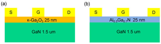
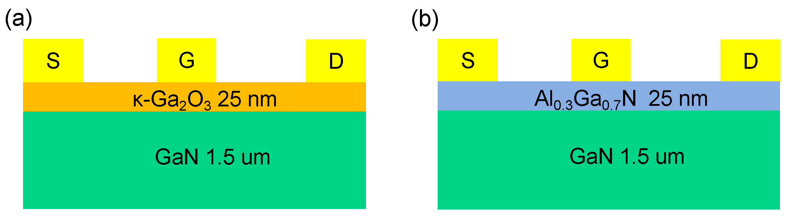
The κ-Ga2O3/GaN HEMT consists of a 25 nm-thick κ-Ga2O3 barrier layer and a 1.5 μm-thick GaN channel layer, as shown in Figure 1a. An Al0.3Ga0.7N/GaN HEMT is also investigated for comparison (Figure 1b). The width of both HEMTs is 100 μm. The gate length (LG), gate-source distance (LGS) and gate-drain distance (LDS) were set to 2 μm, 3 μm and 3 μm, respectively. The source and drain electrodes were defined as Ohmic contacts, while the gate electrode was defined as a Schottky contact with a work function of 5.0 eV [29]. In the present simulations, the gate was modeled as an ideal Schottky contact with a fixed work function, enabling us to clarify the intrinsic electrostatic modulation induced by the κ-Ga2O3/GaN polarization discontinuity and the barrier thickness. However, in realistic devices, the effective gate barrier height and threshold voltage can be affected by the detailed band alignment at the metal/κ-Ga2O3 or dielectric/κ-Ga2O3 interface, as well as by interfacial dipoles and trap states. Therefore, the calculated threshold-voltage values should be interpreted as idealized trends. Experimental techniques such as angle-resolved XPS, UPS, and C-V characterization are required to determine the actual band offsets and validate the simulated gate-control behavior [30]. We assume that κ-Ga2O3/Al0.3Ga0.7N was grown along the [001] direction upon the polar plane (0001) of Ga-faced GaN with spontaneous polarization opposite to the z-axis. Considering the difference in crystalline structure and large lattice mismatch, the κ-Ga2O3 film was considered fully relaxed, eliminating piezoelectric polarization (PPE), and only spontaneous polarization (PSP) was considered [21,26].
Figure 1.
Cross-section structure of (a) κ-Ga2O3/GaN and (b) AlGaN/GaN HEMTs.
The electrical characteristics of the two HEMTs were calculated using the TCAD device simulator Silvaco Atlas (version 5.0.10.R). The models included a parallel electric field model for velocity saturation, Shockley-Read-Hall, an incomplete ionization model and polarization model. All calculations were based on the Fermi-Dirac statistics [29,31]. The density of states of conduction band for κ-Ga2O3 was estimated to be 2.95 × 1018 cm−3, based on an effective electron mass (mn*) of 0.24 m0 [32]. The dielectric constant () of 32 was used for κ-Ga2O3 [7]. The material parameters, including bandgap energy (Eg), conduction band offset between the barrier layer and GaN (ΔEc), electron effective mass relative to free electron mass (mn*/m0), εr, and PSP, for κ-Ga2O3, Al0.3Ga0.7N and GaN are listed in Table 1 [7,32,33,34]. An Al mole fraction of 0.30 was selected for the reference AlGaN/GaN HEMT because Al0.3Ga0.7N is commonly used in conventional GaN-based HEMTs to achieve a relatively high polarization-induced 2DEG density while avoiding excessive lattice mismatch and material degradation [35]. Thus, Al0.3Ga0.7N/GaN serves as a representative benchmark for evaluating the potential advantage of the κ-Ga2O3/GaN heterostructure. The κ-Ga2O3 barrier and GaN channel were treated as unintentionally doped, and the 2DEG was mainly induced by polarization discontinuity rather than intentional donor doping. For the p-GaN-gated structure, the acceptor concentration in the p-GaN cap layer was varied from 1 × 10¹⁷ to 1 × 1018 cm−3 to study the threshold-voltage shift.
Table 1.
Key material parameters for GaN, κ-Ga2O3 and AlN in simulations.
3. Results and Discussion
3.1. Comparison of κ-Ga2O3/GaN and AlGaN/GaN
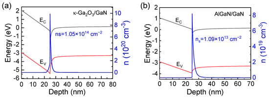
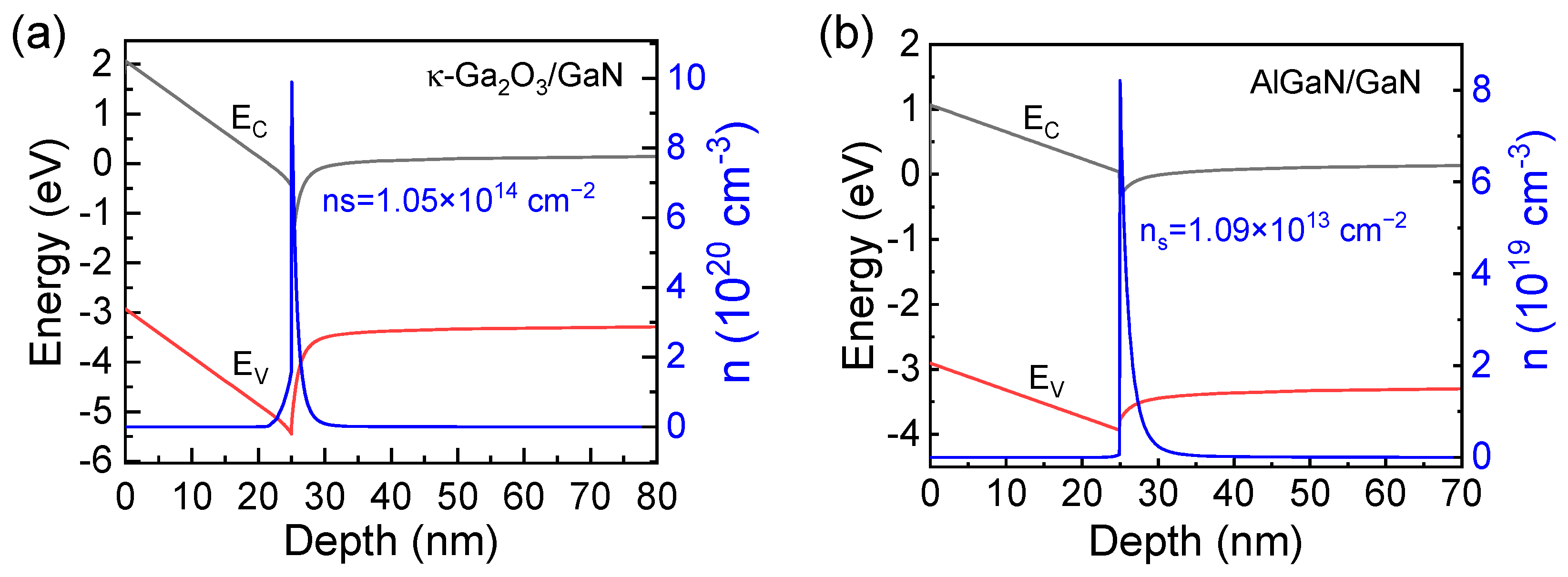
Figure 2a presents the calculated band structure and electron density distribution of the κ-Ga2O3/GaN heterojunction. The conduction band (EC) and valence band (EV) exhibit a pronounced linear bending across the κ-Ga2O3 barrier layer, which originates from the strong polarization fields in κ-Ga2O3/GaN heterostructure. At the κ-Ga2O3/GaN heterointerface, a conduction band offset of 1.38 eV is formed [34], creating a triangular potential well on the GaN side that serves to confine charge carriers. The electron concentration shows a distinct, sharp peak localized at the interface, confirming the formation of a 2DEG. The peak volume concentration reaches 9.90 × 1020 cm−3, corresponding to a sheet electron density (ns) of 1.05 × 1014 cm−2. For comparison, the band structure and electron density distribution of the conventional AlGaN/GaN heterojunction are calculated (Figure 2b). A confined 2DEG is also formed due to the polarization discontinuity at the Al0.3Ga0.7N/GaN interface. The peak density of the 2DEG is about 8.21 × 1019 cm−3, corresponding to a sheet concentration ns of 1.09 × 1013 cm−2, which is in line with the experimental observations [36]. Compared with the κ-Ga2O3/GaN heterojunction, the Al0.3Ga0.7N/GaN system exhibits a weaker polarization-induced electric field, a shallower potential well, and a significantly lower 2DEG sheet density. The κ-Ga2O3/GaN heterojunction achieves a 2DEG sheet density one order of magnitude higher than that of Al0.3Ga0.7N/GaN, exceeding the reported upper limit of 6 × 1013 cm−2 for AlN/GaN heterojunctions [37,38]. This superior performance originates from the stronger polarization-induced electric field and deeper potential well in κ-Ga2O3/GaN, demonstrating its excellent carrier confinement capability for high-power electronic devices.
Figure 2.
Energy band and electron density distribution for (a) κ-Ga2O3/GaN and (b) AlGaN/GaN heterostructures with the barrier thickness of 25 nm. ns is the sheet concentration obtained by integrating n.
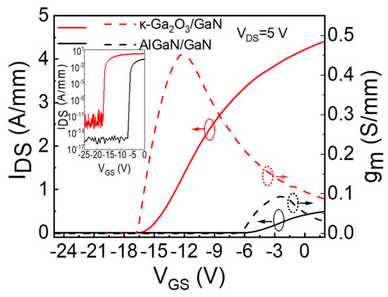
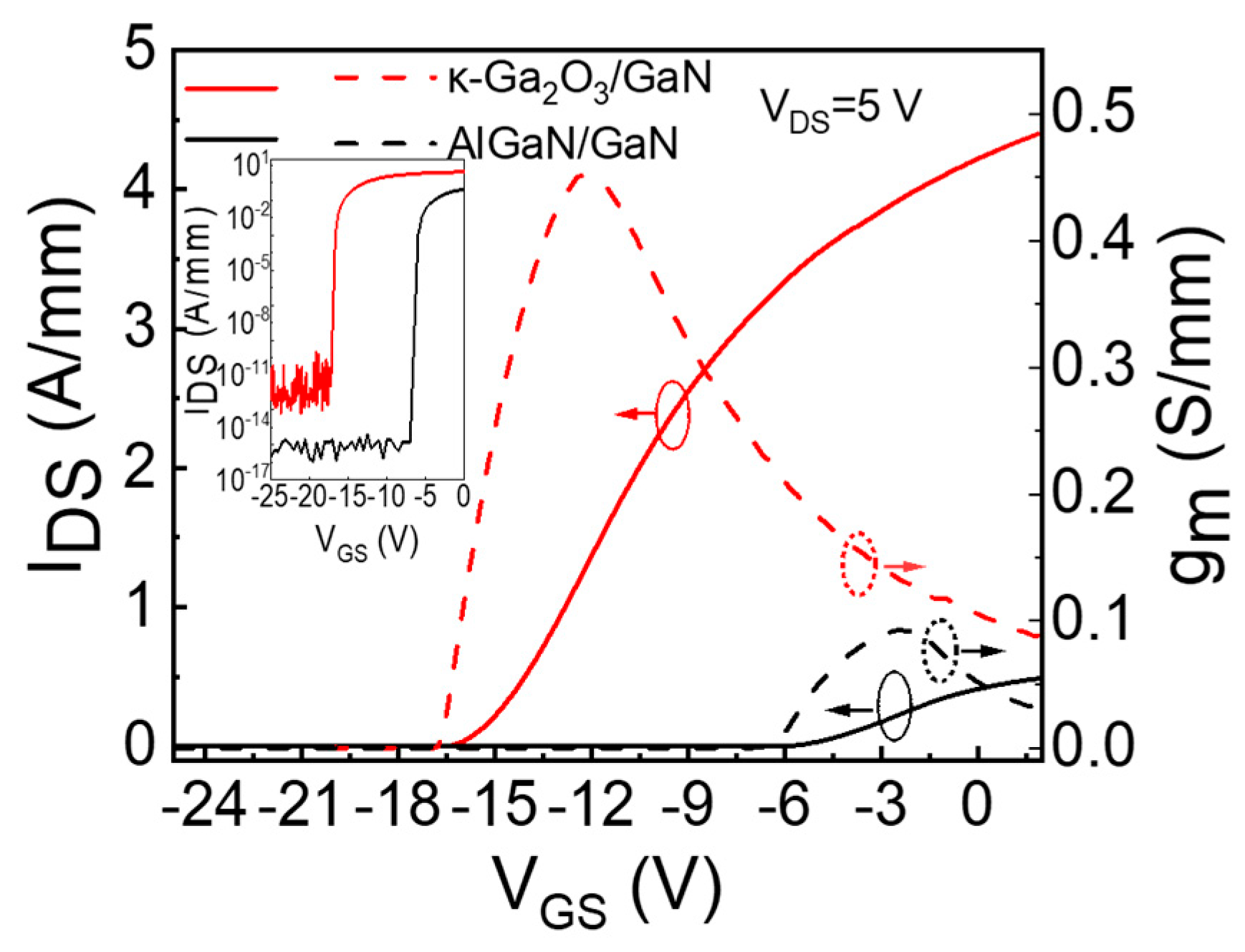
Figure 3 shows the transfer characteristics at the drain-source voltage VDS = 5 V. Drain current density, IDS, and transconductance as a function of gate-source voltage, VGS, are plotted. As illustrated, the maximum drain current density (ID,max) for the κ-Ga2O3/GaN and the AlGaN/GaN reaches 4.40 and 0.49 A/mm at VGS = 2 V, respectively. The ID,max of κ-Ga2O3/GaN is approximately one order of magnitude higher than that of AlGaN/GaN due to the higher 2DEG density at the κ-Ga2O3/GaN interface [39]. Additionally, the gm,max of κ-Ga2O3/GaN HEMT (0.45 S/mm) is about 5 times higher than that of AlGaN/GaN HEMT (0.09 S/mm). Further, as shown in the inset of Figure 3, the ION/IOFF ratio is about 1013 for the AlGaN/GaN and 1012 for the κ-Ga2O3/GaN with LG = 2 μm. A distinct discrepancy in reverse leakage current is observed between the two HEMT structures. The different off-state current levels of the two HEMTs are closely related to their different polarization-induced electrostatics. Because the κ-Ga2O3/GaN heterostructure possesses a much higher 2DEG density, the channel is more difficult to fully deplete under the same negative gate bias, resulting in a higher residual subthreshold current. Since detailed trap-assisted leakage mechanisms were not explicitly included in the present simulation, the leakage characteristics should be understood as idealized trends associated with polarization-induced charge control.
Figure 3.
IDSVGS and gmVGS for the κ-Ga2O3/GaN and AlGaN/GaN HEMTs at VDS = 5 V. The inset is the transfer characteristics in logarithmic scale for the κ-Ga2O3/GaN and the reference AlGaN/GaN HEMTs.
Based on the data, we extracted the threshold voltage (Vth) for both HEMTs via a constant-current method. Vth is defined as the gate voltage when IDS reaches 10 μA/mm in the subthreshold region [40,41]. The Vth values for the κ-Ga2O3/GaN and AlGaN/GaN are −16.8 V and −6.2 V, respectively. The κ-Ga2O3/GaN HEMT has a more negative Vth compared with the AlGaN/GaN HEMT. This behavior can be attributed to the higher 2DEG density at the κ-Ga2O3/GaN interface. Additionally, we calculated the subthreshold swing (SS). The SS values are 84.0 mV/decade for AlGaN/GaN HEMT, and 63.2 mV/decade, approaching the near-ideal range, for the κ-Ga2O3/GaN HEMT [42]. This implies that the polarization-induced higher-density 2DEG at the κ-Ga2O3/GaN interface enables the device to achieve a high-power density and a low power consumption [43].
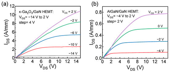
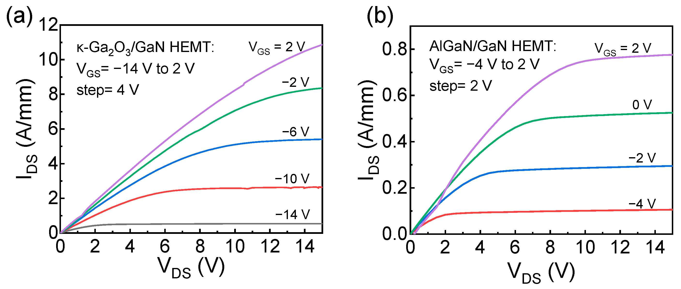
The output characteristics are presented in Figure 4. For the κ-Ga2O3/GaN HEMT, the maximum drain current density is 10.87 A/mm at VDS = 15 V, VGS = 2 V. For the AlGaN/GaN, the maximum drain current density is only 0.78 A/mm. The on-resistance (RON), extracted from the linear region of the case of VGS = 2 V, is 0.89 Ω·mm for the κ-Ga2O3/GaN and 10.21 Ω·mm for the AlGaN/GaN. It means that κ-Ga2O3/GaN has a lower conduction loss in comparison with AlGaN/GaN. The findings confirm that κ-Ga2O3/GaN is a promising candidate to address the challenges of high-power applications.
Figure 4.
IDSVDS for (a) the κ-Ga2O3/GaN and (b) AlGaN/GaN.
The very high 2DEG density predicted for κ-Ga2O3/GaN heterostructures is beneficial for high current drivability. Meanwhile, carrier mobility constitutes another key factor determining the practical performance of κ-Ga2O3/GaN HEMTs. The actual channel mobility and dynamic device performance may be limited by dislocations, native surface traps on κ-Ga2O3 barrier layer, and κ-Ga2O3/GaN interface roughness and traps. These nonidealities can introduce Coulomb scattering, trap-assisted leakage, and current collapse [44,45]. Therefore, high-quality epitaxial growth and interface engineering are expected to be critical for realizing the full potential of κ-Ga2O3/GaN HEMTs. High-k passivation layers and nanolaminate dielectrics grown by ALD or PEALD, such as HfO2/La2O3-based stacks used in AlGaN/GaN systems, may provide possible routes to suppress surface states and improve carrier transport [46]. For κ-Ga2O3/GaN devices, further studies are needed to evaluate the dielectric/κ-Ga2O3 band alignment, threading dislocations and native surface states within the κ-Ga2O3 epitaxial layer, as well as trap density at the κ-Ga2O3/GaN heterointerface to optimize overall electrical performance.
3.2. Effect of Barrier Thickness
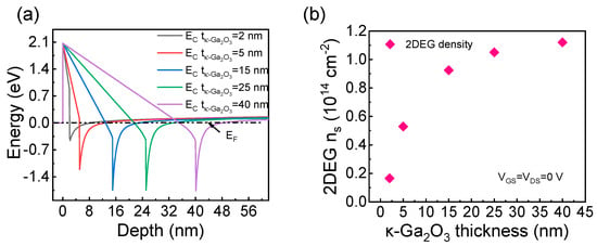
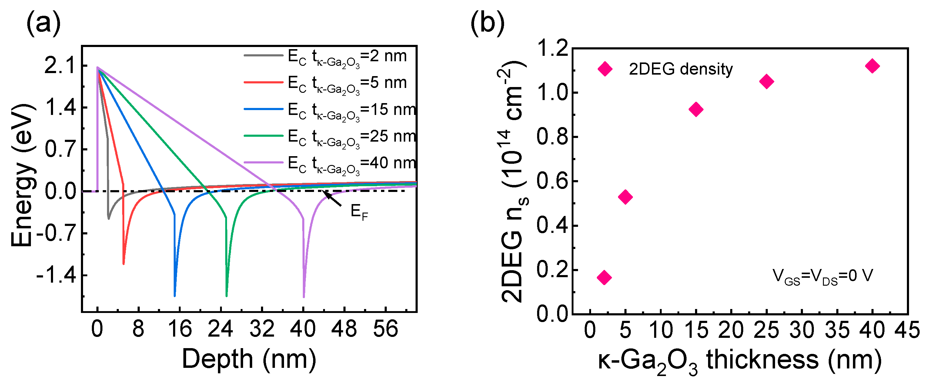
Now, we investigate the influence of κ-Ga2O3 thickness on the conduction band and 2DEG concentration for the κ-Ga2O3/GaN HEMT. As shown in Figure 5a, the Fermi level penetrates into the conduction band, leading to the formation of a triangular quantum well for all the thicknesses we studied. This causes the generation of 2DEG due to polarization-induced electron transfer from donor-like surface states on the top surface of the barrier layer to the GaN conduction band at the interface. The 2DEG density increases with κ-Ga2O3 thickness and gradually approaches saturation with a value of 1.12 × 1014 cm−2 when the thickness is around 40 nm within the investigated range (Figure 5b). This behavior originates from the electrostatic balance between the polarization field and the screening field generated by the transferred electrons. A thicker κ-Ga2O3 barrier produces a larger potential drop and promotes electron transfer to the interface, while the accumulated 2DEG screens the polarization field and limits further increase in sheet density. Therefore, in the ideal model, the 2DEG density is expected to saturate rather than increase indefinitely [47,48]. In practical devices, however, an excessively thick κ-Ga2O3 layer may introduce defects, roughness, strain relaxation, and trap states, which can reduce the effective carrier density and mobility. Thus, the optimized barrier thickness should consider both the saturated 2DEG density and the carrier mobility degradation caused by trap states, defects and interface quality issues.
Figure 5.
(a) Conduction band profiles and (b) 2DEG sheet concentrations of the κ-Ga2O3/GaN heterostructure with varying κ-Ga2O3 thickness.
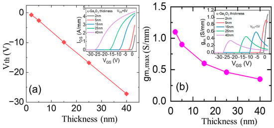
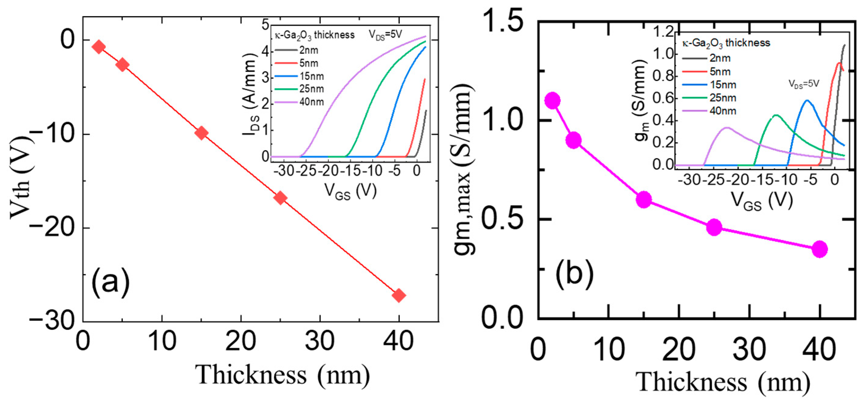
Vth and gm,max, as a function of κ-Ga2O3 thickness, are plotted in Figure 6. The transfer characteristics are also given. The value of Vth is negative (Figure 6a), and its absolute value increases with the barrier thickness due to the deepening of the quantum well. It indicates that one can achieve the desired Vth by tuning the thickness of the κ-Ga2O3 barrier. In addition, the maximum drain current also increases with κ-Ga2O3 thickness due to the enhanced electron density in the channel.
Figure 6.
Vth (a) and gm,max (b) as a function of κ-Ga2O3 thickness for the κ-Ga2O3/GaN HEMTs. The insets are gmVGS and IDSVGS with various thicknesses of κ-Ga2O3, respectively.
The peak transconductance (Figure 6b) decreases with the increase in barrier thickness, owing to the strong impact of the lowering gate capacitance for thicker barriers [48]. It implies that the HEMT suffers from loss of gate control with the increase in κ-Ga2O3 thickness. After careful analysis, we observed that he gm,max reaches 1.08 S/mm when the barrier layer is 2 nm. For this thin barrier, the maximum drain current is close to 2.0 A/mm (see the insets of Figure 6). The value is still much larger than that of conventional AlGaN/GaN HEMT. It can be concluded that the κ-Ga2O3/GaN heterostructure is suitable for fabricating ultra-thin devices, which maintains a large drain current and a high transconductance.
3.3. Effect of p-GaN Gate
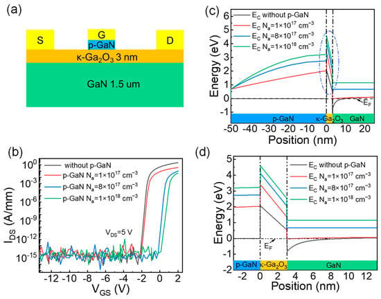
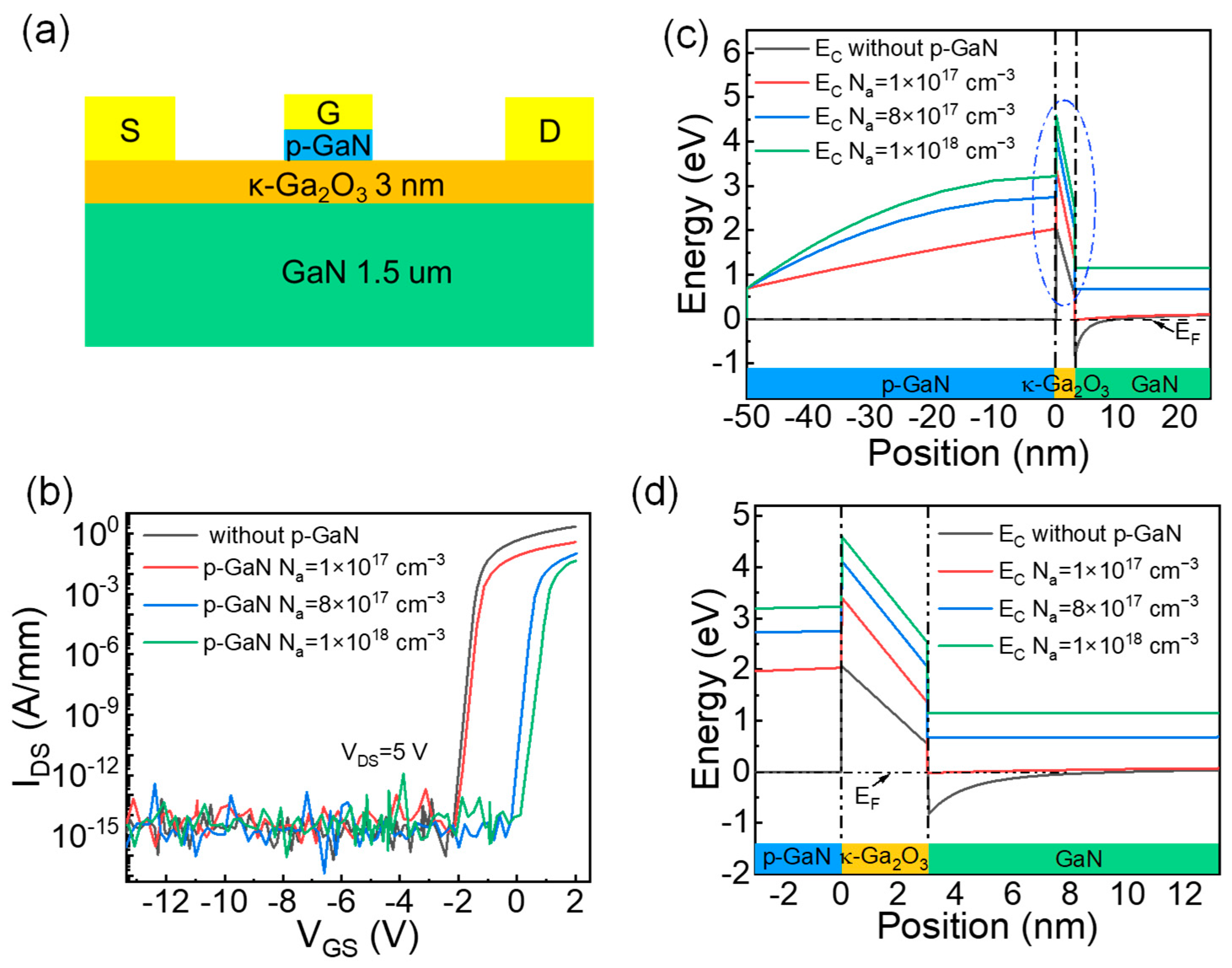
The above κ-Ga2O3/GaN HEMTs display a normally on operation due to the presence of a 2DEG channel at zero gate bias. However, normally off enhancement mode devices with positive threshold voltages are more desirable in power electronic applications, especially in the design of fail-safe power switches and RF power amplifiers [48,49]. To realize the normally off operation, a p-GaN gate layer was introduced at the top of the channel layer, as shown in Figure 7a. The thicknesses of the κ-Ga2O3 barrier and p-GaN cap layer were set to be 3 nm and 50 nm, respectively.
Figure 7.
(a) Schematic structure of the p-GaN gated κ-Ga2O3/GaN HEMT. (b) Transfer characteristics and (c) Ec at VGS = VDS = 0 V for the κ-Ga2O3/GaN HEMTs with and without p-GaN layer. Na denotes the acceptor concentration in the p-GaN layer, and EF represents the Fermi level. The magnified view of the circled region in (c) is displayed in (d).
From the transfer characteristics of HEMTs (shown in Figure 7b), we found that the κ-Ga2O3/GaN HEMT without a cap layer exhibits a threshold voltage of −1.50 V at VDS = 5 V and a maximum drain current density of 2.26 A/mm at VGS = 2 V. For the p-GaN capped devices, Vth shifts positively as the acceptor concentration in the p-GaN layer increases above 8 × 1017 cm−3, implying the realization of enhancement-mode operation. To understand the reason for the positive shift in Vth, we plot the Ec diagrams in Figure 7c. For the heterostructure without the p-GaN layer, the conduction band edge lies below the Fermi level near the interface. The p-type conductivity of the GaN cap layer effectively lifts up the potential, depletes the 2DEG and consequently results in the positive shift in Vth [50]. It should be noted that the incorporation of a p-GaN cap layer does not guarantee normally off operation. An appropriate choice of the acceptor concentration of p-GaN is crucial for efficiently depleting the 2DEG and realizing a normally off operation.
It should be noted that a κ-Ga2O3 thickness of 3 nm is adopted for the p-GaN-gated structure. This ultrathin barrier yields a reduced 2DEG density and a less negative threshold voltage, which enables full depletion of the channel via the p-GaN cap layer. For a thicker κ-Ga2O3 barrier, such as 25 nm, the much higher polarization-induced 2DEG density would make the threshold voltage more negative, and the same p-GaN cap may become insufficient to realize normally off operation. In that case, stronger depletion would be required through a higher acceptor concentration, a thicker p-GaN cap, gate recess engineering, high-work-function gate metals, or dielectric/interface charge engineering. Therefore, the design of p-GaN-gated κ-Ga2O3/GaN HEMTs involves a trade-off between high current density and normally off operation [51].
Although the p-GaN cap layer can deplete the 2DEG and shift the threshold voltage positively, the threshold voltage of a practical p-GaN-gated κ-Ga2O3/GaN HEMT may also be affected by surface and interfacial layers [52]. Native oxide vacancies, residual interlayers, fixed charges, interface dipoles, and trap states at the metal/p-GaN, p-GaN/κ-Ga2O3, or κ-Ga2O3/GaN interfaces can modify the local band bending and further alter the equilibrium 2DEG sheet density as well as threshold voltage. Therefore, surface passivation processes and careful interface control are required for reproducible normally off operation.
Because experimental demonstrations of complete κ-Ga2O3/GaN HEMTs, especially p-GaN-gated normally off devices, remain limited, the present simulation results should be regarded as predictive design guidelines rather than fully benchmarked device datasets, highlighting the necessity of further experimental verification. Hall measurements can be used to determine the 2DEG density and mobility; C–V measurements can evaluate charge control and threshold behavior; and XPS/UPS or angle-resolved XPS can determine the band offsets and band bending at the gate and p-GaN/κ-Ga2O3 interfaces. Such systematic experimental characterizations would enable comprehensive verification of device performance and establish a direct quantitative correlation among interfacial band alignment, p-GaN-mediated channel depletion, and threshold voltage shift.
4. Conclusions
In summary, we have systematically investigated the 2DEG characteristics and performance of κ-Ga2O3/GaN HEMTs through numerical simulations, in comparison with conventional AlGaN/GaN devices. Owing to the strong polarization effect of κ-Ga2O3, the κ-Ga2O3/GaN heterostructure yields an ultrahigh interfacial 2DEG sheet concentration of ~1.05 × 1014 cm−2, nearly one order of magnitude higher than that of conventional AlGaN/GaN heterostructures. The enhanced 2DEG density enables a maximum drain current density of 4.40 A/mm, a peak transconductance of 0.45 S/mm, and a markedly reduced on-resistance of 0.89 Ω·mm in the κ-Ga2O3/GaN HEMT at the barrier thickness of 25 nm and VGS = 2 V. Furthermore, the influence of barrier thickness on the electronic properties has been clarified. The absolute value of Vth increases with the barrier thickness, and the peak transconductance decreases with the increase in barrier thickness. The interfacial 2DEG density exhibits saturation behavior at a barrier thickness of 40 nm, with a saturated value of 1.12 × 1014 cm−2. This tunability enables flexible control of threshold voltage and output performance.
Moreover, by integrating a 50 nm-thick p-GaN cap layer with an acceptor concentration exceeding 8.0 × 1017 cm−3 into the 3 nm-thick κ-Ga2O3 barrier-based GaN HEMT, the interfacial 2DEG can be effectively depleted, enabling the successful realization of normally off operation with a positive threshold voltage of 0.92 V. Our findings reveal the significant advantages of κ-Ga2O3/GaN heterostructures for high-performance and normally off power electronics, and provide important physical insights and design guidelines for next-generation polarization-engineered devices.
Author Contributions
Conceptualization and methodology, Y.Z.; investigation, J.H.; formal analysis, C.H. and Y.D.; data curation, Q.C. and K.F.; writing—review and editing, D.Q. and G.X. All authors have read and agreed to the published version of the manuscript.
Funding
This work is supported by the National Natural Science Foundation of China (62241407, 62304238, 62425403, 62234007, 62293521, U21A20503, U21A2071, and 62004183), the National Key R&D Program of China (2022YFB3605403), Major Projects of Natural Sciences of University in Jiangsu Province of China (25KJA510011) and the Qinglan Project of Jiangsu Province of China.
Institutional Review Board Statement
Not applicable.
Informed Consent Statement
Not applicable.
Data Availability Statement
Data will be made available on request.
Conflicts of Interest
The authors declare that they have no known competing financial interests or personal relationships that could have appeared to influence the work reported in this paper.
References
- Guo, Y.; Qin, Y.; Porter, M.; Yang, Z.; Xiao, M.; Wang, Y.; Popa, D.; Efthymiou, L.; Cheng, C.; Cheng, K.; et al. 10 kV E-mode GaN HEMT: Physics for breakdown voltage upscaling. Appl. Phys. Lett. 2025, 127, 042102. [Google Scholar] [CrossRef] [Scilit]
- Islam, N.; Mohamed, M.F.P.; Khan, M.F.A.J.; Falina, S.; Kawarada, H.; Syamsul, M. Reliability, Applications and Challenges of GaN HEMT Technology for Modern Power Devices: A Review. Crystals 2022, 12, 1581. [Google Scholar] [CrossRef] [Scilit]
- Higashiwaki, M.; Kuramata, A.; Murakami, H.; Kumagai, Y. State-of-the-art technologies of gallium oxide power devices. J. Phys. D Appl. Phys. 2017, 50, 333002. [Google Scholar] [CrossRef] [Scilit]
- Eller, B.S.; Yang, J.; Nemanich, R.J. Polarization Effects of GaN and AlGaN: Polarization Bound Charge, Band Bending, and Electronic Surface States. J. Electron. Mater. 2014, 43, 4560–4568. [Google Scholar] [CrossRef] [Scilit]
- Wan, L.; Sun, P.; Liu, X.; Chen, D.; Que, X.; Yao, S.; Li, G. A highly efficient method to fabricate normally-off AlGaN/GaN HEMTs with low gate leakage via Mg diffusion. Appl. Phys. Lett. 2020, 116, 023504. [Google Scholar] [CrossRef] [Scilit]
- Maccioni, M.B.; Fiorentini, V. Phase diagram and polarization of stable phases of (Ga1−xInx)2O3. Appl. Phys. Express 2016, 9, 041102. [Google Scholar] [CrossRef] [Scilit]
- Yusa, S.; Oka, D.; Fukumura, T. High-κ dielectric ε-Ga2O3 stabilized in a transparent heteroepitaxial structure grown by mist CVD at atmospheric pressure. Cryst. Eng. Comm. 2020, 22, 381–385. [Google Scholar] [CrossRef] [Scilit]
- Mezzadri, F.; Calestani, G.; Boschi, F.; Delmonte, D.; Bosi, M.; Fornari, R. Crystal Structure and Ferroelectric Properties of epsilon-Ga2O3 Films Grown on (0001)-Sapphire. Inorg. Chem. 2016, 55, 12079–12084. [Google Scholar] [CrossRef] [Scilit] [PubMed]
- Kim, J.; Tahara, D.; Miura, Y.; Kim, B.G. First-principle calculations of electronic structures and polar properties of (κ, ε)-Ga2O3 Applied Physics Express. Appl. Phys. Express 2018, 11, 061101. [Google Scholar] [CrossRef] [Scilit]
- Mazzolini, P.; Varley, J.B.; Parisini, A.; Sacchi, A.; Pavesi, M.; Bosio, A.; Bosi, M.; Seravalli, L.; Janzen, B.M.; Marggraf, M.N.; et al. Engineering shallow and deep level defects in κ-Ga2O3 thin films: Comparing metal-organic vapour phase epitaxy to molecular beam epitaxy and the effect of annealing treatments. Mater. Today Phys. 2024, 45, 101463. [Google Scholar] [CrossRef] [Scilit]
- Karthik Ram, M.; Dahlberg, H.; Wernersson, L.-E. Cryogenic Ferroelectricity of HZO Capacitors on a III–V Semiconductor. IEEE Electron Device Lett. 2024, 45, 1827–1830. [Google Scholar] [CrossRef] [Scilit]
- Wang, P.; Wang, D.; Mondal, S.; Hu, M.; Liu, J.; Mi, Z. Dawn of nitride ferroelectric semiconductors: From materials to devices. Semicond. Sci. Technol. 2023, 38, 043002. [Google Scholar] [CrossRef] [Scilit]
- Leone, S.; Fornari, R.; Bosi, M.; Montedoro, V.; Kirste, L.; Doering, P.; Benkhelifa, F.; Prescher, M.; Manz, C.; Polyakov, V.; et al. Epitaxial growth of GaN/Ga2O3 and Ga2O3/GaN heterostructures for novel high electron mobility transistors. J. Cryst. Growth 2020, 534, 125511. [Google Scholar] [CrossRef] [Scilit]
- Cho, S.B.; Mishra, R. Epitaxial engineering of polar ε-Ga2O3 for tunable two-dimensional electron gas at the heterointerface. Appl. Phys. Lett. 2018, 112, 162101. [Google Scholar] [CrossRef] [Scilit]
- Wang, Y.; Guan, Y.; Zhang, C.; Cao, J.; Chen, X.; Ouyang, Q.; Wong, Y.H.; Hu, G.; Tan, C.K. Indium alloying in ε-Ga2O3 for polarization and interfacial charge tuning. Appl. Phys. Lett. 2025, 126, 022112. [Google Scholar] [CrossRef] [Scilit]
- Ranga, P.; Cho, S.B.; Mishra, R.; Krishnamoorthy, S. Highly tunable, polarization-engineered two-dimensional electron gas in ε-AlGaO3/ε-Ga2O3 heterostructures. Appl. Phys. Express 2020, 13, 061009. [Google Scholar] [CrossRef] [Scilit]
- Wang, Y.; Cao, J.; Song, H.; Zhang, C.; Xie, Z.; Wong, Y.H.; Tan, C.K. Polarization engineering of two-dimensional electron gas at ε-(AlxGa1–x)2O3/ε-Ga2O3 heterostructure. Appl. Phys. Lett. 2023, 123, 142103. [Google Scholar] [CrossRef] [Scilit]
- Kuang, Y.; Chen, X.; Ma, T.; Du, Q.; Zhang, Y.; Hao, J.; Ren, F.-F.; Liu, B.; Zhu, S.; Gu, S.; et al. Band Alignment and Enhanced Interfacial Conductivity Manipulated by Polarization in a Surfactant-Mediated Grown κ-Ga2O3/In2O3 Heterostructure. ACS Appl. Electron. Mater. 2021, 3, 795–803. [Google Scholar] [CrossRef] [Scilit]
- Polyakov, A.Y.; Nikolaev, V.I.; Pechnikov, A.I.; Yakimov, E.B.; Karpov, S.Y.; Stepanov, S.I.; Shchemerov, I.V.; Vasilev, A.A.; Chernykh, A.V.; Kuznetsov, A.; et al. Two-dimensional hole gas formation at the κ-Ga2O3/AlN heterojunction interface. J. Alloys Compd. 2023, 936, 168315. [Google Scholar] [CrossRef] [Scilit]
- Nikolaev, V.I.; Stepanov, S.I.; Pechnikov, A.I.; Shapenkov, S.V.; Scheglov, M.P.; Chikiryaka, A.V.; Vyvenko, O.F. HVPE Growth and Characterization of ε-Ga2O3 Films on Various Substrates. ECS J. Solid State Sci. Technol. 2020, 9, 045104. [Google Scholar] [CrossRef] [Scilit]
- Li, Y.; Xiu, X.; Xu, W.; Zhang, L.; Zhao, H.; Xie, Z.; Tao, T.; Chen, P.; Liu, B.; Zhang, R.; et al. Pure-phase κ-Ga2O3 layers grown on c-plane sapphire by halide vapor phase epitaxy. Superlattices Microstruct. 2021, 152, 106845. [Google Scholar] [CrossRef] [Scilit]
- Oshima, Y.; Víllora, E.G.; Matsushita, Y.; Yamamoto, S.; Shimamura, K. Epitaxial growth of phase-pure ε-Ga2O3 by halide vapor phase epitaxy. J. Appl. Phys. 2015, 118, 085301. [Google Scholar] [CrossRef] [Scilit]
- Tahara, D.; Nishinaka, H.; Morimoto, S.; Yoshimoto, M. Stoichiometric control for heteroepitaxial growth of smooth ε-Ga2O3 thin films onc-plane AlN templates by mist chemical vapor deposition. Jpn. J. Appl. Phys. 2017, 56, 078004. [Google Scholar] [CrossRef] [Scilit]
- Xia, X.; Chen, Y.; Feng, Q.; Liang, H.; Tao, P.; Xu, M.; Du, G. Hexagonal phase-pure wide band gap ε-Ga2O3 films grown on 6H-SiC substrates by metal organic chemical vapor deposition. Appl. Phys. Lett. 2016, 108, 202103. [Google Scholar] [CrossRef] [Scilit]
- Kang, H.Y.; Yeom, M.J.; Yang, J.Y.; Choi, Y.; Lee, J.; Park, C.; Yoo, G.; Kyu Chung, R.B. Epitaxial κ-Ga2O3/GaN heterostructure for high electron-mobility transistors. Mater. Today Phys. 2023, 31, 101002. [Google Scholar] [CrossRef] [Scilit]
- Chen, Y.; Ning, H.; Kuang, Y.; Yu, X.-X.; Gong, H.-H.; Chen, X.; Ren, F.-F.; Gu, S.; Zhang, R.; Zheng, Y.; et al. Band alignment and polarization engineering in κ-Ga2O3/GaN ferroelectric heterojunction. Sci. China Phys. Mech. Astron. 2022, 65, 277311. [Google Scholar] [CrossRef] [Scilit]
- Wang, J.; Guo, H.; Zhu, C.-Z.; Cai, Q.; Yang, G.-F.; Xue, J.-J.; Chen, D.-J.; Tong, Y.; Liu, B.; Lu, H.; et al. ε-Ga2O3: A Promising Candidate for High-Electron-Mobility Transistors. IEEE Electron Device Lett. 2020, 41, 1052–1055. [Google Scholar] [CrossRef] [Scilit]
- Qu, A.; Xie, Z.; Wang, Y.; Hu, G.; Tan, C.-K. Effect of Acceptor-Type Traps in GaN Buffer Layer on Current Collapse of ε-Ga2O3/GaN HEMTs. J. Electron. Mater. 2025, 54, 3086–3096. [Google Scholar] [CrossRef] [Scilit]
- Ge, M.; Li, Y.; Zhu, Y.; Chen, D.; Wang, Z.; Tan, S. An improved design for e-mode AlGaN/GaN HEMT with gate stack β-Ga2O3/p-GaN structure. J. Appl. Phys. 2021, 130, 035703. [Google Scholar] [CrossRef] [Scilit]
- Chakraborty, S.; Kim, T.-W. Comprehensive Schottky Barrier Height Behavior and Reliability Instability with Ni/Au and Pt/Ti/Pt/Au on AlGaN/GaN High-Electron-Mobility Transistors. Micromachines 2022, 13, 84. [Google Scholar] [CrossRef] [Scilit] [PubMed]
- Song, K.; Zhang, H.; Fu, H.; Yang, C.; Singh, R.; Zhao, Y.; Sun, H.; Long, S. Normally-off AlN/β-Ga2O3 field-effect transistors using polarization-induced doping. J. Phys. D Appl. Phys. 2020, 53, 345107. [Google Scholar] [CrossRef] [Scilit]
- Guo, S.-D.; Du, H.-M. Piezoelectric properties of Ga2O3: A first-principle study. Eur. Phys. J. B 2020, 93, 7. [Google Scholar] [CrossRef] [Scilit]
- Krishna, S.; Lu, Y.; Liao, C.-H.; Khandelwal, V.; Li, X. Band alignment of orthorhombic Ga2O3 with GaN and AlN semiconductors. Appl. Surf. Sci. 2022, 599, 153901. [Google Scholar] [CrossRef] [Scilit]
- Reddy, P.; Bryan, I.; Bryan, Z.; Tweedie, J.; Washiyama, S.; Kirste, R.; Mita, S.; Collazo, R.; Sitar, Z. Charge neutrality levels, barrier heights, and band offsets at polar AlGaN. Appl. Phys. Lett. 2015, 107, 091603. [Google Scholar] [CrossRef] [Scilit]
- Jayasakthi, M.; Ramesh, R.; Arivazhagan, P.; Loganathan, R.; Prabakaran, K.; Balaji, M.; Baskar, K. Structural and optical characterization of AlGaN/GaN layers. J. Cryst. Growth 2014, 401, 527–531. [Google Scholar] [CrossRef] [Scilit]
- Hsu, L.; Walukiewicz, W. Effect of polarization fields on transport properties in AlGaN/GaN heterostructures. J. Appl. Phys. 2001, 89, 1783–1789. [Google Scholar] [CrossRef] [Scilit]
- Cao, Y.; Jena, D. High-mobility window for two-dimensional electron gases at ultrathin AlN/GaN heterojunctions. Appl. Phys. Lett. 2007, 90, 182112. [Google Scholar] [CrossRef] [Scilit]
- Ambacher, O.; Foutz, B.; Smart, J.; Shealy, J.R.; Weimann, N.G.; Chu, K.; Murphy, M.; Sierakowski, A.J.; Schaff, W.J.; Eastman, L.F.; et al. Two dimensional electron gases induced by spontaneous and piezoelectric polarization in undoped and doped AlGaN/GaN heterostructures. J. Appl. Phys. 2000, 87, 334–344. [Google Scholar] [CrossRef] [Scilit]
- Zimmermann, T.; Deen, D.; Cao, Y.; Simon, J.; Fay, P.; Jena, D.; Xing, H.G. AlN/GaN Insulated-Gate HEMTs With 2.3 A/mm Output Current and 480 mS/mm Transconductance. IEEE Electron Device Lett. 2008, 29, 661–664. [Google Scholar] [CrossRef] [Scilit]
- Zhang, Y.; Sun, M.; Joglekar, S.J.; Fujishima, T.; Palacios, T. Threshold voltage control by gate oxide thickness in fluorinated GaN metal-oxide-semiconductor high-electron-mobility transistors. Appl. Phys. Lett. 2013, 103, 033524. [Google Scholar] [CrossRef] [Scilit]
- Ma, C.; Chen, H.; Zhou, C.; Huang, S.; Yuan, L.; Roberts, J.; Chen, K.J. ON-state critical gate overdrive voltage for fluorine-implanted enhancement-mode AlGaN/GaN high electron mobility transistors. J. Appl. Phys. 2011, 110, 114514. [Google Scholar] [CrossRef] [Scilit]
- Lu, H.; Hou, B.; Yang, L.; Niu, X.; Si, Z.; Zhang, M.; Wu, M.; Mi, M.; Zhu, Q.; Cheng, K.; et al. AlN/GaN/InGaN Coupling-Channel HEMTs for Improved gm and Gain Linearity. IEEE Trans. Electron Devices 2021, 68, 3308–3313. [Google Scholar] [CrossRef] [Scilit]
- Rao, G.P.; Lenka, T.R.; Singh, R.; Nguyen, H.P.T. Simulation modelling of III-nitride/β-Ga2O3 HEMT for emerging high-power nanoelectronics applications. J. Korean Phys. Soc. 2022, 81, 876–884. [Google Scholar] [CrossRef] [Scilit]
- Zanato, D.; Gokden, S.; Balkan, N.; Ridley, B.K.; Schaff, W.J. The effect of interface-roughness and dislocation scattering on low temperature mobility of 2D electron gas in GaN/AlGaN. Semicond. Sci. Technol. 2004, 19, 427–432. [Google Scholar] [CrossRef] [Scilit]
- Zhang, J.; Hao, Y.; Zhang, J.; Ni, J. The mobility of two-dimensional electron gas in AlGaN/GaN heterostructures with varied Al content. Sci. China Ser. F Inf. Sci. 2008, 51, 780–789. [Google Scholar] [CrossRef] [Scilit]
- Cao, D.; Cheng, X.; Xie, Y.; Li, X.; Wang, Z.; Xia, C.; Zheng, L.; Xu, D.; Shen, L.; Yu, Y. Properties of HfO2/La2O3 nanolaminate films grown on an AlGaN/GaN heterostructure by plasma enhanced atomic layer deposition. RSC Adv. 2014, 4, 36828–36833. [Google Scholar] [CrossRef] [Scilit]
- Ibbetson, J.P.; Fini, P.T.; Ness, K.D.; DenBaars, S.P.; Speck, J.S.; Mishra, U.K. Polarization effects, surface states, and the source of electrons in AlGaN/GaN heterostructure field effect transistors. Appl. Phys. Lett. 2000, 77, 250–252. [Google Scholar] [CrossRef] [Scilit]
- Smorchkova, I.P.; Elsass, C.R.; Ibbetson, J.P.; Vetury, R.; Heying, B.; Fini, P.; Haus, E.; DenBaars, S.P.; Speck, J.S.; Mishra, U.K. Polarization-induced charge and electron mobility in AlGaN/GaN heterostructures grown by plasma-assisted molecular-beam epitaxy. J. Appl. Phys. 1999, 86, 4520–4526. [Google Scholar] [CrossRef] [Scilit]
- He, J.; Cheng, W.C.; Wang, Q.; Cheng, K.; Yu, H.; Chai, Y. Recent Advances in GaN-Based Power HEMT Devices. Adv. Electron. Mater. 2021, 7, 2001045. [Google Scholar] [CrossRef] [Scilit]
- Meneghini, M.; Hilt, O.; Wuerfl, J.; Meneghesso, G. Technology and Reliability of Normally-Off GaN HEMTs with p-Type Gate. Energies 2017, 10, 153. [Google Scholar] [CrossRef] [Scilit]
- Greco, G.; Iucolano, F.; Roccaforte, F. Review of technology for normally-off HEMTs with p-GaN gate. Mater. Sci. Semicond. Process. 2018, 78, 96–106. [Google Scholar] [CrossRef] [Scilit]
- Wu, T.-L.; Marcon, D.; Bakeroot, B.; De Jaeger, B.; Lin, H.C.; Franco, J.; Stoffels, S.; Van Hove, M.; Roelofs, R.; Groeseneken, G.; et al. Correlation of interface states/border traps and threshold voltage shift on AlGaN/GaN metal-insulator-semiconductor high-electron-mobility transistors. Appl. Phys. Lett. 2015, 107, 093507. [Google Scholar] [CrossRef] [Scilit]

Disclaimer/Publisher’s Note: The statements, opinions and data contained in all publications are solely those of the individual author(s) and contributor(s) and not of MDPI and/or the editor(s). MDPI and/or the editor(s) disclaim responsibility for any injury to people or property resulting from any ideas, methods, instructions or products referred to in the content. |
© 2026 by the authors. Licensee MDPI, Basel, Switzerland. This article is an open access article distributed under the terms and conditions of the Creative Commons Attribution (CC BY) license.