


1. Error in Figure
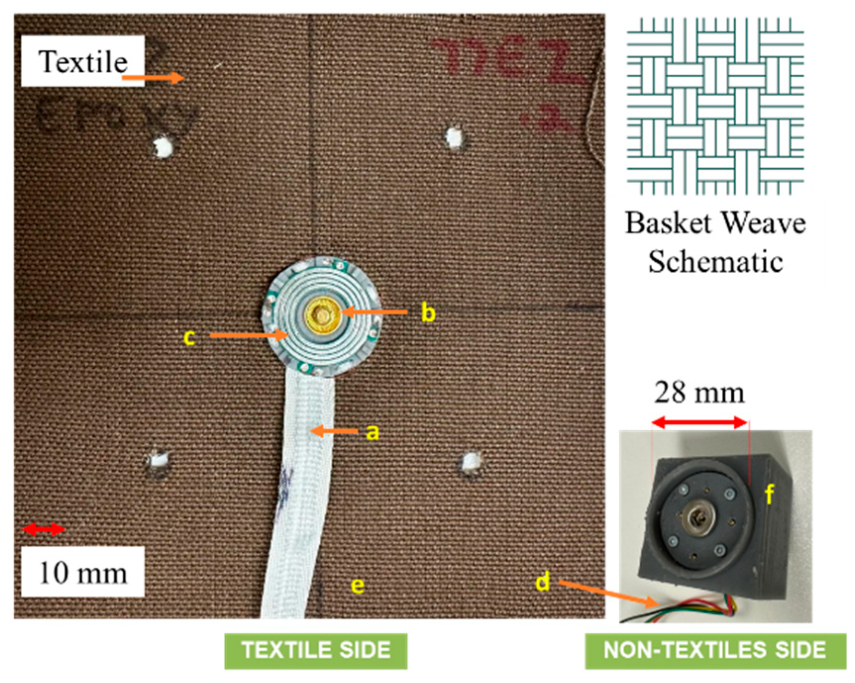
In the original publication [1], there was a typographical error in Figure 4. The dimension is not 280 mm but 28 mm as appears below. The authors apologize for any inconvenience caused and state that the scientific conclusions are unaffected.
2. Blurred Figures
Figures 1, 7, and 9 have been replaced with higher quality ones.
Figure 1.
Three interconnect technologies based on conductivity and flexibility.
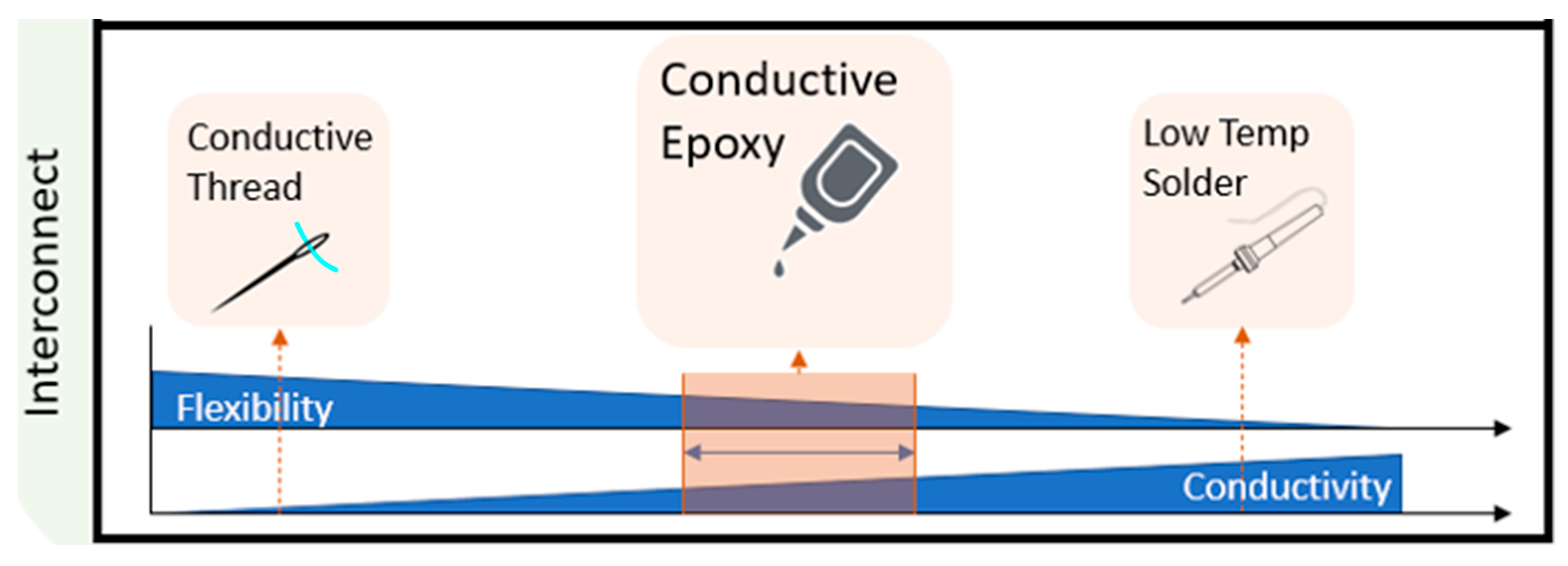
Figure 7.
(a) Force gauge. (b) IMADA motorized stand.
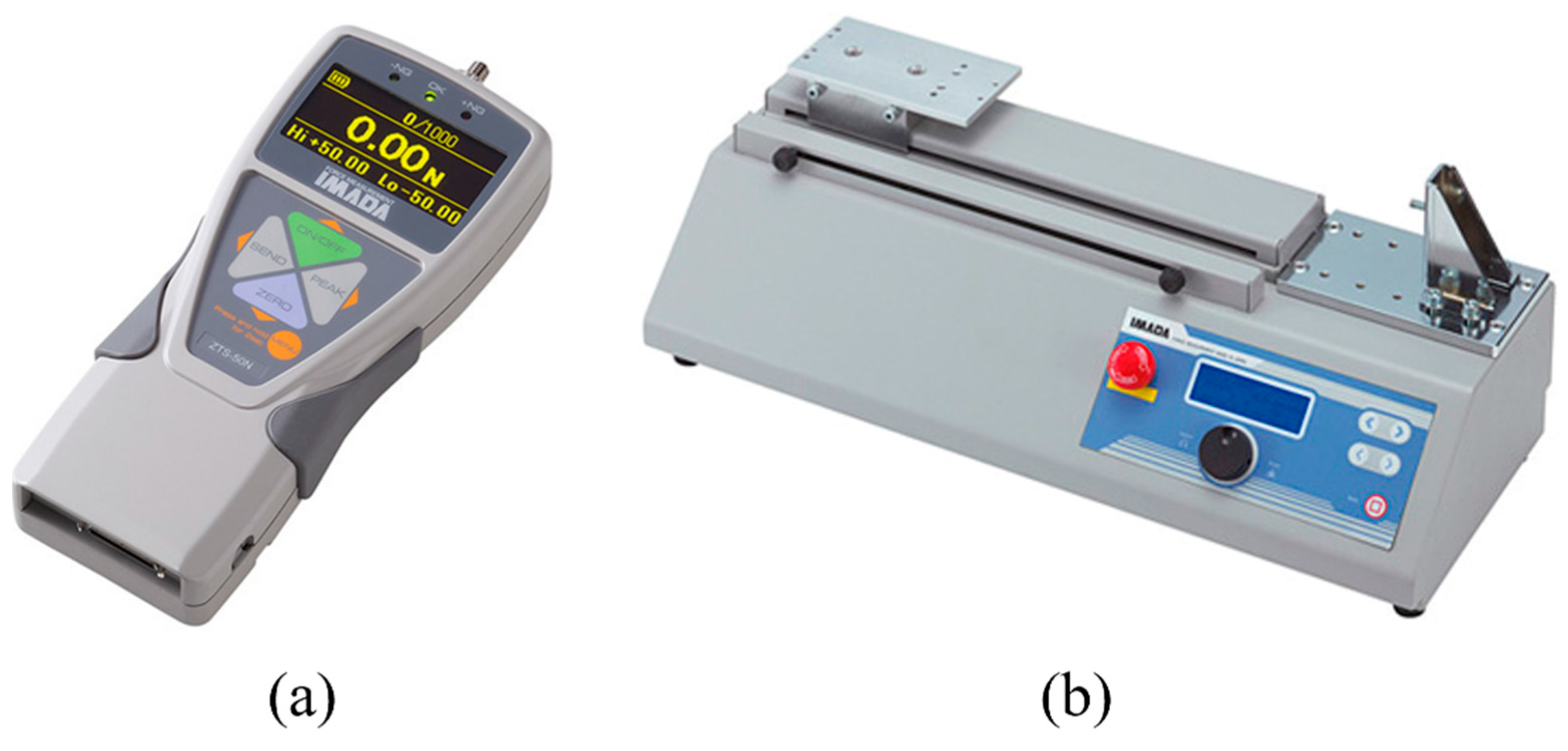
Figure 9.
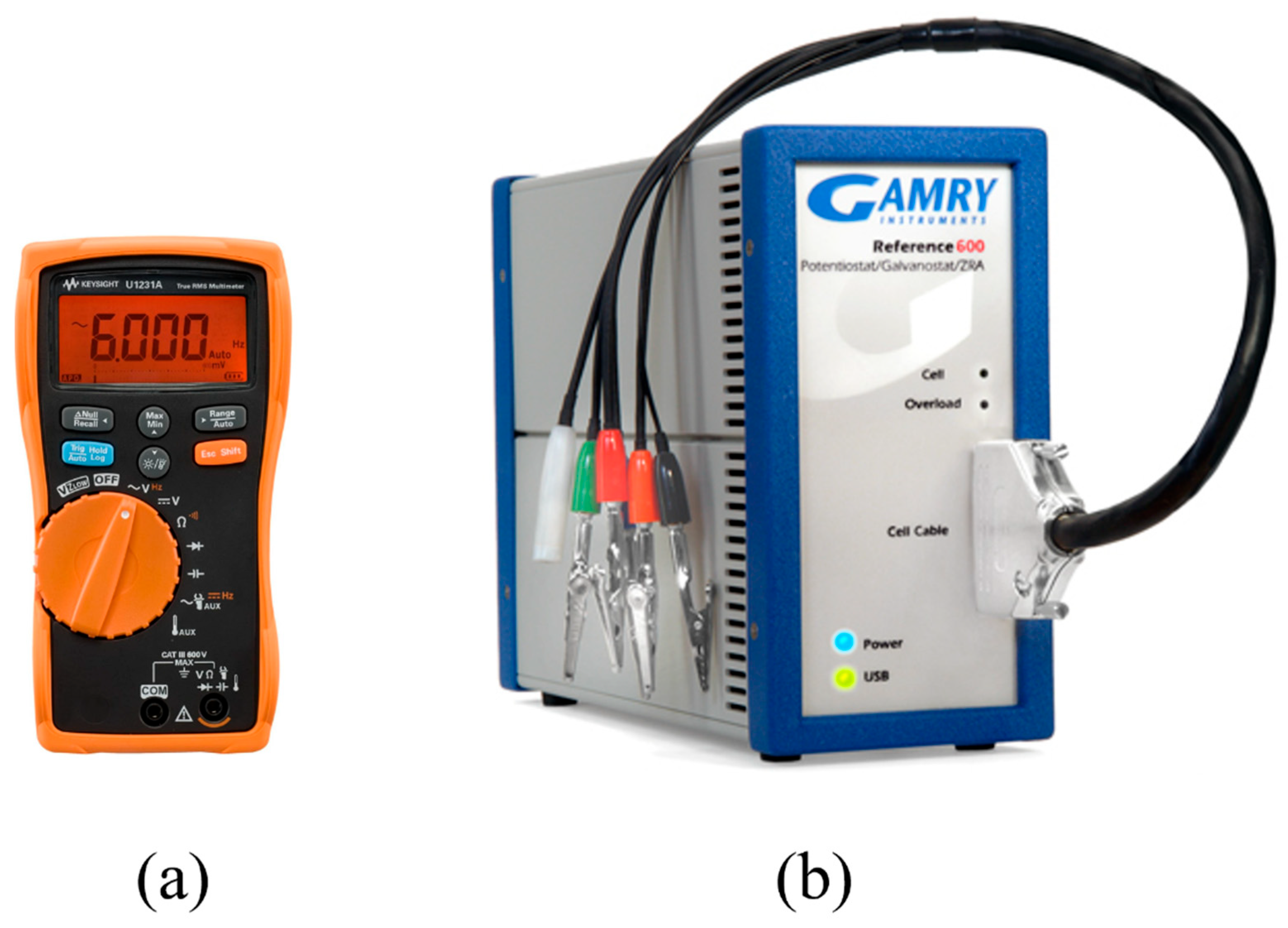
(a) Keysight U1231A multimeter. (b) Gamry device.
3. Text Correction
There was a typographical error in the Conclusion section. A correction has been made to Conclusion Section in the first paragraph as follows. The authors apologize for any inconvenience caused and state that the scientific conclusions are unaffected.
“Wearable connectors are critical components of wearable systems as they perform the important task of transferring monitored physiological or environmental signals to electronics for data amplification or display. In this study, we designed and developed detachable mechanical connectors that can be integrated into a garment in the form of snaps. Results showed that unlike the connectors of low and medium unmating forces, which could withstand all 5000 cycles, the connector with a high mating–unmating force level failed before 1000 mating–unmating cycles were complete. Connectors mating–unmating at low force levels gave the highest overall conductance in all interconnects. Epoxy interconnects performed the best over 5000 cycles at the low force level. For the medium force level, conductive stitches showed a higher conductance as they are mechanically stronger and more flexible than the other two interconnect types. Overall, the conductance of all the interconnects was low (less than 1 siemens). The empirical data evidence how important it is to engineer materials and to design interconnect methods, mating–unmating forces, and mating–unmating cycles for a particular application of wearable connectors.”
4. Text Correction
There was a typographical error and a correction has been made to Section 2.2 in the last paragraph. The authors apologize for any inconvenience caused and state that the scientific conclusions are unaffected. The corrected paragraph is below.
“The MTS Q-test machine (Berlin, Germany) was used to characterize the mechanical strength of the three interconnects. Under the standard ASTM D2261—Fabric Tongue Tear Test setting [31]—the textile side connector was pulled away from the fabric substrate and the textile cable until separation. For the accurate characterization of interconnect strength, no means of mechanical attachment was added. The test was performed in an angle same to the snap mating–unmating direction. It was observed that the interconnect using conductive stitches showed the highest pull force—99.45 N for snap. For the other two interconnect methods, the pull force stayed around 9–10 N. The force seemed to be recorded when the textile cable broke, indicating the strength of the Cu wires before damaging the interconnect itself.”
5. Text Correction
There was a typographical error and a correction has been made to Section 2.3 in the second last paragraph. The authors apologize for any inconvenience caused and state that the scientific conclusions are unaffected. Corrected paragraph is below.
“The impedance magnitude as a function of the frequency was measured for the connector samples using the Gamry Potentiostat (Figure 9b) (Philadelphia, PA, USA). The device was first calibrated and, like the resistance readings, alligator clips of the Gamry were appropriately attached to the hook-up wires on the textile side connector and its corresponding channels on the non-textile side connector. The impedance was measured across frequencies from 100 kHz to 1 MHz for the USB 2.0 and I2C communication protocol. The USB 2.0 protocol was chosen due to its widespread usage, familiarity, and compatibility with various devices [32]. The device recorded 200 points of data across these frequencies from each sample. Impedance was measured at 0 and 5000 cycles with the connectors in the mated position.”
6. Text Correction
There was a typographical error and a correction has been made to the paragraph in Section 3.3. The authors apologize for any inconvenience caused and state that the scientific conclusions are unaffected. The corrected paragraph is below.
“Figure 13a shows a prototype of the example system implemented with the proposed connector. A temperature sensor was stitched to the inner side of a forearm sleeve to be in contact with skin and to monitor the skin temperature. One end of the textile data cable was soldered to the sensor, and another end was soldered to the PCB on the snap connector, to transfer the data from the sensor to the textile side snap connector (plug). The textile side snap connector was attached to the forearm sleeve with non-conductive stitches. Figure 13b shows that the temperature signal was read at the non-textile side snap connector (receptacle) when mated with the textile side connector. This evidences that the snap connector is a miniaturized wearable device that can integrate seamlessly into a garment and look aesthetically pleasing due to its snap form factor. In future, to evaluate the reliability of this connector, it can be compared to a conventional connector under a more controlled experimental setting.”
7. Text Correction
There was a typographical error referring to conductive stitches and a correction has been made to Section 3.1 in the second paragraph, the caption of Figure 11, Table 3, Section 3.2 in the first paragraph, and the caption of Figure 12. The authors apologize for any inconvenience caused and state that the scientific conclusions are unaffected. The corrected paragraph is below.
“Table 2 shows the ANOVA results for the snap connector. The factors of the snap-connecting interface that had a significant effect on the conductance were Force Level (main effect), Interconnect Method (main effect), and Force Level × Interconnect Method (interaction effect). The overall trend in the conductance from force levels (low and medium) across the three interconnect methods (conductive epoxy, conductive stitches, and solder) at every 1000 mating–unmating cycles starting from 0 to 5000 for the snap type of connector can be found in Figure 11.”
“Figure 11. Conductance in the snap connector from two force levels (low and medium) across the three interconnect methods (conductive epoxy, conductive stitches, and solder) at every 1000 mating–unmating cycles starting from 0 to 5000.”
Table 3.
Tukey’s HSD connecting letter report of Force Level x Interconnect Method.
“Figure 12a,b show the impedance magnitude between 100 kHz (or 100,000 Hz) and 1 MHz (or 1,000,000 Hz) frequencies, across the three interconnect methods (conductive epoxy, conductive stitches, and solder) at 0 and 5000 mating–unmating cycles respectively. It can be observed that the impedance of the soldered snap connectors stayed lower as compared to the conductive-epoxied and conductive-stitched samples. At 0 cycles, conductive-stitched interconnect samples had a slightly higher impedance as compared to the conductive-epoxied samples. However, after 5000 cycles, it was observed that the impedance in the conductive-epoxied samples was slightly higher than the conductive-stitched samples. Overall, impedance increased with frequency, but the active increase started from 100 kHz to 1 MHz frequency. This increase was less than 2 ohms.”
“Figure 12. Impedance magnitude of snap connector across the three interconnect methods (conductive epoxy, conductive stitches, and solder) at (a) 0 and (b) 5000 mating–unmating cycles.”
8. Text Correction
There was a typographical error and a correction has been made to Section 3.1 in the sixth paragraph and Section 2.2 in the second paragraph. The authors apologize for any inconvenience caused and state that the scientific conclusions are unaffected. The corrected paragraph is below.
“The least conductance was shown in conductive epoxied samples of medium unmating force levels. This might have been due to the conductive epoxy not being able to withstand the medium unmating force level like conductive stitches. This shows that the conductive epoxy works great for lower unmating forces, but not at the medium unmating force level. As the force level increased, the difference between interconnect methods became ambiguous. The force level seems to have impacted the solder interconnect. The overall conductance at both unmating force levels was low. This could be because of the rigid nature of the solder, which could have led to cracks or the breaking of the solder. Solder showed a relatively lower conductance; however, it did not perform significantly differently than the conductive epoxy and conductive stitches at the medium force level. Therefore, higher force and mating–unmating cycles with solder might not be the best option for the interconnect method.”
9. Text Correction
There was a typographical error citing Figure 6. Figure 6 in the existing text needs to be re-labeled Figure 6a or Figure 6b. A correction has been made to Section 2.2 in the first and second paragraphs. The authors apologize for any inconvenience caused and state that the scientific conclusions are unaffected. The corrected paragraph is below.
“The three interconnect methods used were conductive epoxy, stitches, and solder. Epoxied interconnects were achieved using low-temperature conductive silver epoxy (S-CEP7-SF4) supplied from Sunray Scientific S-CEP7-SF4 (Eatontown, NJ, USA). This is a two-part, silver-filled epoxy-based, electrically conductive adhesive designed by Sunray Scientific. It forms a strong bond with the substrate and circuitry, while maintaining exceptional flexibility. It can offer reduced silver migration properties with our anti-silver migration additive. Madeira HC-40 highly conductive embroidery thread (Freiburg, Germany) with 117/2 dtex linear density and <300 ohm/m resistance was used to make the conductive stitch interconnects. A Juki DDL-8700 industrial sewing machine (Tokyo, Japan) was used to create stitches under the needle thread tension of 1.75 N and the bobbin thread tension of 0.25 N. MG Chemicals 60/40 rosin core leaded solder (Burlington, ON, Canada) with a 0.032” diameter and a melting temperature of 183 °C enabled soldered interconnects. The three interconnect materials were applied to pre-arranged holes (marked with orange arrows in Figure 6a) of the connector body and PCB on the connectors. Conductive stitches were repeated four to five times, and each interconnection hole was filled with the epoxy and solder, respectively. Additional holes were made on the connector body to sew the connector body to the textiles using non-conduction stitches (marked with black arrows in Figure 6a).”
“A textile data cable from WEEL Technology (Greensboro, NC, USA) was used to construct the electric infrastructure for power and data transmission on the fabric surface. The cable was 1.00 mm-wide and 0.70 mm-thick woven tape having a polyester sheath and four copper (Cu) wires inside. The four-wire design was used for the USB 2.0 protocol, as shown in Figure 2. Each Cu wire had 14 filaments with a resistance of approximately 1.5 ohm/m. One end of the cable was unraveled to attach to the hook-up wires. Four Cu wires on the other end were inserted into four pre-arranged holes on the connector body and PCB. These four holes are individually connected to the four concentric conductive electrodes on the PCB, respectively. This makes each Cu wire connected to each conductive ring on PCB using three different interconnect technologies. These concentric electrodes on the PCB are meant to contact the pogo pins on the non-textile side of the connector to make an electrical connection (Figure 6b). The metal stud and socket were used for mechanical connection. A circular/ring design was adopted for the non-directional mating of the textile and the non-textile side of the connector. In the case of the sewn interconnect, the conductive yarn was stitched from the hole of the connector body to a hole adjacent to it on the PCB, in which the Cu wire was encased. The conductive epoxy and solder were placed right on the hole of the PCB. As mentioned above, this assembly of the textile side connector was mechanically sewn to the fabric using a regular sewing thread (non-conductive interconnect), 27-tex cotton-poly spun yarn (marked with black arrows in Figure 6a).”
10. Text Correction
There was a typographical error citing Figure 10, and a correction has been made to Section 3 in the second paragraph. The authors apologize for any inconvenience caused and state that the scientific conclusions are unaffected. The corrected paragraph is below.
“This failure happened regardless of the interconnection method. Conductive-stitched samples have a better attachment between the connector and the fabric due to the presence of four non-conductive and four conductive stitches, whereas the conductive epoxy and solder samples only have four non-conductive stitches. In the case of conductive epoxy (Figure 10a) and conductive stitches (Figure 10b) samples, the metal socket and stud detached from the connector, respectively. In the case of solder (Figure 10c), the unraveling of the non-conductive stitches was observed. This can be due to the mating–unmating force exerted on the connector being much higher for the four non-conductive stitches that hold the connector to the fabric. The solder samples also showed cracks and the breakage of the plastic housing. The excessive force exerted during mating–unmating can cause damage to the connector housing or casing (in this case, the plastic body). Figure 10c shows cracks, fractures, and the breakage of the plastic housing material. Therefore, a very high mating–unmating force can compromise the structural integrity and protection of the connector components.”
Reference
- Ugale, P.; Lingampally, S.; Dieffenderfer, J.; Suh, M. Wearable Solutions: Design, Durability, and Electrical Performance of Snap Connectors and Integrating Them into Textiles Using Interconnects. Textiles 2024, 4, 328–343. [Google Scholar] [CrossRef] [Scilit]
Disclaimer/Publisher’s Note: The statements, opinions and data contained in all publications are solely those of the individual author(s) and contributor(s) and not of MDPI and/or the editor(s). MDPI and/or the editor(s) disclaim responsibility for any injury to people or property resulting from any ideas, methods, instructions or products referred to in the content. |
© 2026 by the authors. Licensee MDPI, Basel, Switzerland. This article is an open access article distributed under the terms and conditions of the Creative Commons Attribution (CC BY) license.