


Abstract
A software tool for realistic simulation of DDS output phase noise under non-ideal conditions is presented. Unlike approaches that rely solely on ideal clock scaling or require detailed device-specific characterization, the proposed method combines an ideal scaled contribution with an optional quantization floor and a compact phenomenological residual-noise model that captures output-stage limitations. The tool accepts sparse clock phase-noise data and DDS parameters, reconstructs the output spectrum, and exports ADIsimPLL-compatible models. Validation against AD9912 (50 MHz, 150 MHz) and AD9915 (123 MHz, 978 MHz) datasheet curves shows agreement within 2–3 dB for most offsets, with deviations up to 5 dB only at 10 Hz for the 978 MHz case. The approach enables phase-noise reconstruction from limited published data and supports hybrid DDS-driven PLL synthesizer studies.
1. Introduction
Direct digital synthesis (DDS) is a digitally controlled signal generation technique in which the output frequency is set by a programmable tuning word referenced to a clock source [1]. DDS is attractive in practice due to its high frequency resolution, fast tuning capability, and phase-continuous operation [1,2].
From the spectral purity viewpoint, however, predicting DDS output phase noise is considerably more difficult than predicting the nominal output frequency [2]. Reported DDS measurements indicate that the phase noise scales down approximately as 1/f2 only until the limit imposed by the output stage is reached [2]. The same work also shows that spur-related effects can redistribute power from the white noise floor, making ideal clock scaling alone insufficient for realistic DDS phase-noise prediction. This creates a practical engineering problem. If only ideal clock scaling is applied, the predicted DDS output spectrum may become unrealistically optimistic in offset frequency regions where internal DDS mechanisms and the analog output path determine the actual floor and slope structure [2]. At the same time, an excessively device-specific description is less suitable for comparative analysis and synthesizer-level design studies. In practice, a usable intermediate model is needed to translate available clock source data and DDS operating conditions into a realistic output phase-noise profile suitable for DDS-driven PLL synthesis studies.
The importance of accurate link modelling is also evident in 5G radio relay planning, where signal level distribution and fading directly affect system performance [3]. Phase-noise characterization of frequency synthesizers is equally critical for such systems [1,4].
The present work is driven by this engineering need. Rather than aiming at a purely theoretical noise model, the objective is to provide a practical simulation framework that can reliably reconstruct DDS output phase noise from the limited data typically available in datasheets. To this end, a software tool that combines ideal clock scaling relations with a compact phenomenological residual-noise model is developed. The resulting framework enables realistic prediction of DDS output phase-noise behavior under non-ideal operating conditions and is intended to support early-stage trade-off studies in hybrid synthesizer design.
2. Theoretical Background and Modeling Basis
2.1. Signal and Phase-Noise Representation
The starting point is the standard representation of a noisy carrier:
where is the nominal amplitude, is the fractional amplitude fluctuation, and is the random phase fluctuation [2]. In this notation, the noise is described through the single-sided power spectral densities and , and the phase-noise spectrum is commonly approximated by a polynomial law of the form .
For phase-noise analysis, the more widely plotted quantity is the single-sideband phase noise , related to the phase-fluctuation spectrum by:
This relation is fundamental for the simulation tool because it determines how the contributions must be combined (link can be found in Supplementary Materials). Since physical superposition applies to power spectral densities in linear units, all modeled terms must first be converted to , summed there, and only then transformed back to in dBc/Hz. The same convention is used in the literature on DAC and DDS phase-noise characterization [4].
2.2. DDS Frequency Generation and Ideal Phase-Noise Scaling
A conventional DDS is governed by the modulo-D phase accumulation rule:
where N is the tuning word and D = 2m is set by the phase-accumulator length m [2]. This mechanism yields the nominal output frequency:
The corresponding frequency resolution is:
where fCLK is the system clock frequency. These relations explain both the frequency agility and the extremely fine frequency resolution that distinguish DDS operation from many analog alternatives [1,2].
From the phase-noise viewpoint, the key result is that, under an ideal noise-free synthesis core, the input phase-time fluctuation is transferred to the output while the phase unit scales with frequency [2]:
In logarithmic single-sideband form, this becomes [5]:
This scaling law constitutes the ideal reference-based component used by the software tool. However, reported DDS measurements also show that the ideal 1/f02 tendency does not continue indefinitely. Once the down-scaled input contribution reaches the limit imposed by the DDS output stage, the measured spectrum no longer follows the ideal scaling expressed by Equation (7).
2.3. Quantization, Spurs, and the Need for a Residual Model
A first non-ideal contribution arises from DAC quantization. In DDS systems, the finite DAC resolution q sets a lower bound on the achievable white noise floor, and under the usual white-quantization approximation the corresponding coefficient can be written as [2]:
Accordingly, the optional quantization contribution included in the total model is taken as , that is, as a frequency-independent white phase-noise term derived from Equation (8). This term is used in the software as an optional quantization contribution, enabled when the DAC resolution is known and quantization noise is to be included explicitly.
A realistic DDS output, however, cannot be described by white quantization alone. Because the phase accumulator must be truncated before phase-to-amplitude conversion, the DDS introduces a deterministic phase error rather than a purely random one. Reported analyses show that this error has a sawtooth-like form, is sampled at the clock frequency, and produces harmonics that extend beyond the Nyquist band and are aliased back into the useful spectrum as discrete spurs [2]. The same analyses also show that these spurs modify the apparent broadband floor, so the resulting spectrum cannot be represented adequately by ideal clock scaling plus white quantization only [2]. Recent hardware-oriented DDS designs have employed cubic Hermite interpolation to mitigate amplitude quantization spurs, achieving significant SFDR improvements at the cost of additional logic resources [6].
Further non-ideal contributions originate in the DAC and analog output path. In addition to quantization and phase truncation, practical DDS outputs are affected by DAC nonlinearity, switching transients, clock feedthrough, and output-stage limitations [6]. Experimental studies further show that, once the clock-scaled contribution has been reduced sufficiently, the measured close-in spectrum is often limited by the DDS output stage and associated low-frequency mechanisms rather than by the ideal scaling law itself. From a practical viewpoint, the DDS follows clock scaling only over part of the offset-frequency range, while the rest is captured by an additional model term [2].
For this reason, the present work introduces a phenomenological residual phase-noise model intended as an engineering approximation of the deviation from ideal clock-scaled behavior. In the implemented form, the residual contribution is written as:
where the coefficients represent residual white, flicker, and 1/f2 components, respectively. In practical use, the simulated spectrum is not allowed to follow ideal clock scaling toward unrealistically low values once the output-stage-related limit is reached. Instead, the spectrum is constrained by an output-stage-related floor term once the floor-limited region is reached, so that the reconstructed spectrum remains consistent with the observed behavior of practical DDS implementations. In the following, denotes this effective residual contribution as used by the simulation model. The total modeled DDS phase-noise spectrum is therefore formed in linear units as:
where denotes the optional quantization term. The final single-sideband result is obtained as:
The resulting model combines the clock-scaled contribution with optional quantization and residual-noise terms for practical DDS phase-noise prediction. In this form, it also provides a reusable phase-noise representation suitable for further simulation of hybrid synthesizer architectures.
2.4. Use of the Proposed Model in Hybrid DDS-Driven PLL Architecture
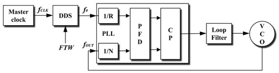
Hybrid DDS-driven PLL architectures are widely used in modern frequency synthesis to combine the fine resolution of direct digital synthesis [7] with the spectral purity of phase-locked loops [1]. The system-level role of the proposed approach is illustrated in Figure 1. While the PLL subsystem can be evaluated in established environments such as ADIsimPLL, the required phase-noise descriptions of the master clock, DDS output, and VCO are not always available in directly reusable form. The developed tool addresses this limitation by generating phase-noise models from data typically available in technical documentation or extracted from published phase-noise plots, thereby enabling simulation of hybrid synthesizer architectures using realistic input data and supporting results that are closer to practical behavior.
Figure 1.
Conceptual role of the proposed phase-noise model in a DDS-driven PLL synthesizer architecture.
For example, the hybrid opto-electronic synthesizer reported in [8] uses a DDS clocked by an ultra-low noise 10 GHz reference to achieve wideband tunability (8–12 GHz) with phase noise as low as −156 dBc/Hz at 10 kHz offset. Similarly, a dual PLL frequency synthesizer for a cesium atomic clock [9] employs a DDS to generate a 7.368 MHz reference signal for the second phase-locked loop. The proposed simulation tool could assist in the early-stage design of such systems by estimating the DDS output phase noise under non-ideal conditions.
3. Simulation Methodology and Software Implementation
3.1. Workflow and Simulation Objective
The application was implemented in Python 3.10.11 as a desktop graphical environment using PySide6 version 6.11.0 for the user interface and Matplotlib version 3.10.7 for visualization. The tool is intended for early-stage evaluation of hybrid frequency synthesizer architectures in which fine frequency resolution and wide tuning capability must be achieved without neglecting phase-noise performance. In such studies, the designer typically selects a master clock source, a DDS device, a VCO, and PLL parameters, and then seeks realistic simulation results before hardware implementation.
While the required phase-noise information is often available in technical documentation, it is not always provided in a form directly suitable for system-level simulation. The purpose of the developed environment is therefore to assist in transforming available source data into reusable phase-noise models for subsequent analysis of standalone DDS solutions and hybrid DDS-driven PLL synthesizers.
3.2. Reference Clock and DDS Data Input
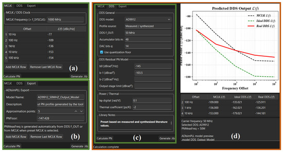
The simulation workflow begins from input data typically available in technical documentation or published measurements. For the reference clock, the procedure is direct: the carrier frequency is entered explicitly, and the phase-noise profile is defined by discrete L(f) values at selected offset frequencies, as shown in Figure 2a. This corresponds to the usual way in which oscillator phase noise is reported in datasheets.
Figure 2.
Main views of the developed DDS phase −noise simulation tool: (a) MCLK input tab, (b) export tab, (c) DDS parameter tab, and (d) overall application view with predicted DDS output spectrum and ADIsimPLL model preview.
For the DDS stage, the parameterization is broader because the output spectrum depends on both nominal operating parameters and device-specific nonideal behavior. In the current implementation, the user may either select a predefined DDS model or enter the parameters manually. The DDS input section includes the output frequency, the accumulator length m, the DAC resolution q, optional activation of the quantization floor, and a residual phase-noise model defined by the coefficients b0, b−1, and b−2, together with an output-stage limit term—Figure 2c.
When an absolute phase-noise plot is available for the selected DDS device, the residual-model coefficients may be estimated graphically from the published spectrum. The white noise coefficient b0 is taken from the flat high-offset region. The flicker coefficient b−1 is obtained from the close-in asymptote with an approximate slope of −10 dB/decade by extending that line toward 1 Hz offset. If a sufficiently distinct −20 dB/decade region is present, b−2 may be estimated in the same manner from the corresponding 1/f2 behavior. In this case, the coefficients are used as engineering estimates derived from datasheet plots, not as directly measured analytical model parameters.
3.3. DDS Output Spectrum Reconstruction Algorithm
The implemented reconstruction algorithm operates on the offset frequency points entered in the MCLK table. First, the ideal DDS contribution is obtained by scaling the entered master-clock phase-noise values with the ratio f0/fCLK according to Equation (7). These values are then converted to linear phase-noise spectral density.
Next, the DDS residual contribution is evaluated on the same offset frequency grid from the coefficients b0, b−1, and b−2, using the form Equation (9). If enabled, the quantization term is added as a constant white contribution derived from the DAC resolution and clock frequency. When specified, the output-stage limit is applied as a lower constraint on the close-in residual spectrum.
The total modelled DDS spectrum is then obtained as the sum of all contributions in linear units. In the final step, the result is converted back to the single sideband representation L(f). Log–log interpolation is applied only for plotting and export purposes, while the main calculation is performed directly on the entered offset frequency points.
3.4. Exporting Phase-Noise Models
The overall application view in Figure 2d combines the reconstructed DDS spectrum with the corresponding model preview, whereas the export panel in Figure 2b provides generation of reusable phase-noise models. In the standard DDS mode, the reconstructed DDS output spectrum is exported as an ADIsimPLL-compatible phase-noise model. The same function also supports separate export of master-clock and VCO phase-noise data when these components are to be represented individually as source blocks. This extends the program from DDS output reconstruction to broader support of standalone DDS and hybrid DDS-driven PLL studies. The ADIsimPLL environment is widely used for designing low-phase-noise PLL synthesizers; for example, a fourth-order RLC loop filter designed with ADIsimPLL was shown to achieve phase noise below −100 dBc/Hz at 1 kHz offset [10].
4. Simulation Results and Model Validation
The developed software tool was evaluated against published phase-noise data for two different DDS devices: the AD9912 and the AD9915.
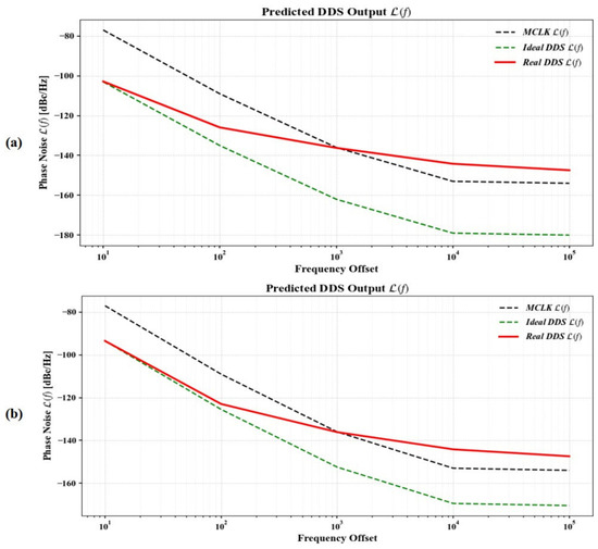
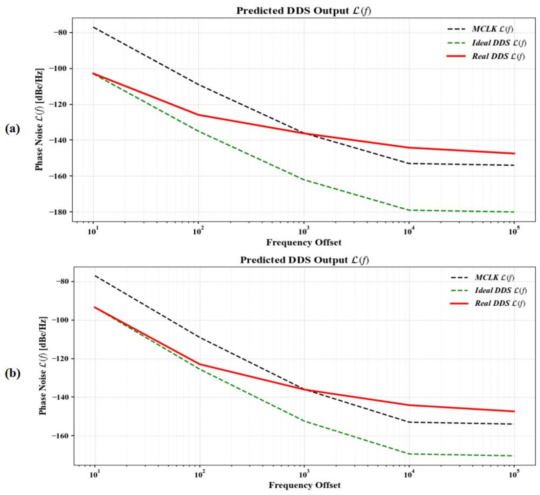
For the AD9912, validation was carried out at output frequencies of 50 MHz and 150 MHz, using the reference clock phase noise of a Wenzel oscillator [11] as reported in [12]. The corresponding simulated spectra are shown in Figure 3. The numerical comparison in Table 1 includes the original datasheet values, which are not generated by the software tool but serve as an independent reference for the reader. The simulated values track the datasheet curves within about 1.5 dB over the reported offset range (100 Hz to 100 kHz).
Figure 3.
Simulated DDS output phase-noise spectrum for the AD9912 at (a) 50 MHz and (b) 150 MHz output frequency with reference clock—Wenzel 1 GHz oscillator.
Table 1.
Comparison between graphically extracted AD9912 datasheet phase-noise values and simulated DDS output phase-noise values.
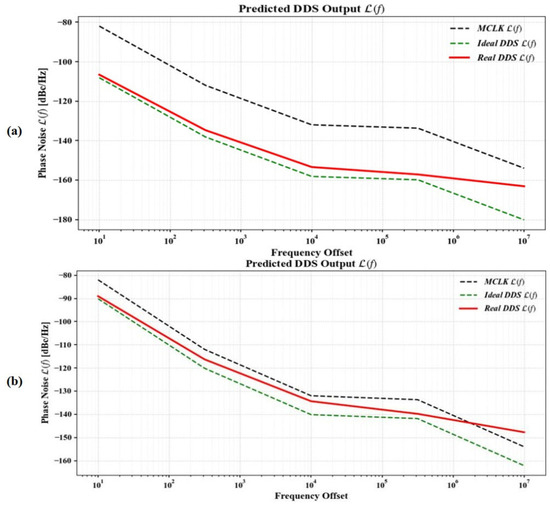
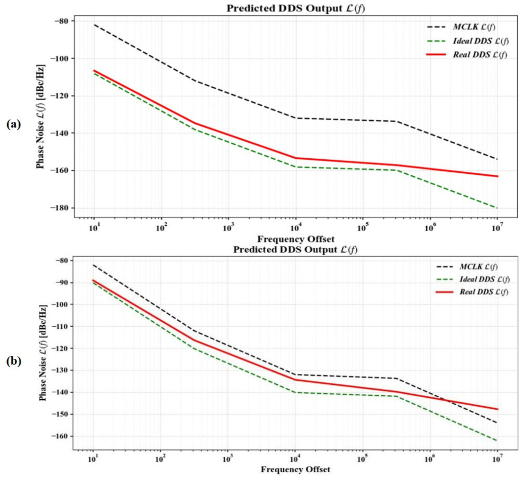
For the AD9915 [13], the reference clock was a Rohde & Schwarz SMA100 signal generator [14] at 2.5 GHz buffered by an ADCLK925, with its phase-noise profile taken from Figure 4 of the AD9915 datasheet [13]. The output spectra were validated at 123 MHz and 978 MHz using the absolute phase-noise curves of the same datasheet [13]; the results are presented in Figure 4 and Table 2.
Figure 4.
Simulated DDS output phase-noise spectrum for the AD9915 at (a) 123 MHz and (b) 978 MHz output frequency with ref. clock—R&S SMA100 at 2.5 GHz buffered by ADCLK925.
Table 2.
Comparison between graphically extracted AD9915 datasheet phase-noise values and simulated DDS output phase-noise values.
As with the AD9912, Table 2 includes the datasheet reference levels to facilitate direct numerical comparison. The agreement is within 2–3 dB for most offsets; the largest deviation (5 dB) occurs at 10 Hz for the 978 MHz output. This increased deviation is attributed to the very steep phase-noise slope at very low offset frequencies, where small errors in the graphically extracted flicker coefficient (b−1) lead to larger absolute differences.
In both cases, the residual model coefficients (b0, b−1, b−2) were estimated graphically from the respective datasheet phase-noise plots following the procedure described in Section 3.2.
An important practical aspect of the AD9912 validation is that the reference clock spectrum was available only as a sparse set of discrete values (four points) [12]. The simulation was therefore carried out under sparse input conditions representative of a realistic engineering situation. For the AD9915, the clock phase noise was given as a denser curve (Figure 4) [13]; nevertheless, the reconstruction still relied on graphical extraction of a limited number of points, maintaining the practical nature of the method.
For engineering-level comparisons and synthesizer-oriented studies, deviations of 3–5 dB at offsets below 100 Hz are generally acceptable, because the close-in phase noise in a typical DDS-driven PLL is dominated by the reference oscillator and loop filter rather than by the residual DDS floor. This tolerance is typical for early-stage evaluation, where low-offset DDS noise is rarely limiting.
In all four tested cases (50 MHz and 150 MHz for AD9912; 123 MHz and 978 MHz for AD9915), the simulated output reproduces the main spectral features expected from practical DDS operation: the close-in decrease associated with the dominant low-frequency contribution (flicker noise), the transition region, and the high-offset floor-limited region.
For comparison, a naive model using only ideal clock scaling (7) (without the residual term) produces deviations exceeding 10 dB at higher offsets, reaching more than 30 dB near 100 kHz in the AD9912 50 MHz case (Figure 3a).
The reconstructed spectrum is only as accurate as the input data used to define both the reference clock spectrum and the residual DDS coefficients. When only a few phase-noise values are available, the result should be regarded as an engineering approximation rather than an exact reconstruction. Nevertheless, by combining the reference clock contribution with a compact non-ideal DDS model, the tool produces spectra consistent with published device behavior for two different DDS families driven by different reference clocks. Overall, the results demonstrate that the tool is suitable for DDS phase-noise reconstruction and for generation of reusable models for subsequent synthesizer-level studies, covering both sparse and moderately dense input data scenarios.
5. Conclusions
A software tool for realistic DDS output phase-noise prediction has been developed and validated against AD9912 and AD9915 devices. The method combines ideal clock scaling with a compact residual-noise model, allowing output spectra to be reconstructed from sparse datasheet data. Validation shows agreement within 2–3 dB for most offsets, with deviations reaching 5 dB only at 10 Hz for the 978 MHz case. Deviations of this magnitude at very low offset frequencies are acceptable for engineering studies because the close-in phase noise in a typical DDS-driven PLL is dominated by the reference oscillator and loop filter, not by the residual DDS floor. The tool exports ADIsimPLL-compatible models, directly bridging device documentation and system-level simulation. While the limitations of graphical coefficient extraction are acknowledged, the results demonstrate that the proposed approach is suitable for rapid early-stage evaluation of hybrid DDS-driven synthesizer architectures. Future work includes automated extraction of residual coefficients from spectral plots using optimization algorithms, which would further reduce manual fitting effort.
Supplementary Materials
The executable version (version v1.0) of the simulation tool is available at the following GitHub repository: https://github.com/ZParunev/Osc_Sim_PN/releases/tag/v1.0 (accessed on 2 September 2026).
Author Contributions
Conceptualization, Z.P. and G.G.; methodology, G.G.; software, Z.P.; formal analysis, G.G.; investigation, Z.P.; resources, G.G.; data curation, Z.P.; writing—original draft preparation, Z.P.; writing—review and editing, G.G.; visualization, Z.P. All authors have read and agreed to the published version of the manuscript.
Funding
This research received no external funding.
Institutional Review Board Statement
Not applicable.
Informed Consent Statement
Not applicable.
Data Availability Statement
Dataset available on request from the author.
Conflicts of Interest
The authors declare no conflicts of interest.
Abbreviations
The following abbreviations are used in this manuscript:
| DAC | Digital-to-analog converter |
| DDS | Direct digital synthesis |
| MCLK | Master clock |
| PLL | Phase-locked loop |
| SFDR | Spurious-free dynamic range |
| VCO | Voltage-controlled oscillator |
References
- Chenakin, A. Microwave Frequency Synthesizers: A Tutorial. IEEE Microw. Mag. 2023, 24, 29–40. [Google Scholar] [CrossRef] [Scilit]
- Calosso, C.E.; Gruson, Y.; Rubiola, E. Phase Noise and Amplitude Noise in DDS. In Proceedings of the 2012 IEEE International Frequency Control Symposium (IFCS); IEEE: Piscataway, NJ, USA, 2012; pp. 777–782. [Google Scholar]
- Iliev, T.; Stoyanov, I.; Mihaylov, G.; Fazylova, A.; Papadopoulou, M.S. Evaluation of Signal Level Distribution in 5G Radio Relay Transmissions. Eng. Proc. 2023, 41, 2. [Google Scholar] [CrossRef] [Scilit]
- Calosso, C.E.; Cárdenas Olaya, A.C.; Rubiola, E. Phase-Noise and Amplitude-Noise Measurement of DACs and DDSs. IEEE Trans. Ultrason. Ferroelectr. Freq. Control 2020, 67, 431–439. [Google Scholar] [CrossRef] [Scilit]
- Annino, B. Low Phase Noise DAC-Based Frequency Synthesis for Fast Hopping Wideband Microwave Applications; Technical Article; Analog Devices: Wilmington, MA, USA, 2021. [Google Scholar]
- Zhou, K.; Xu, Q.; Zhang, T. Optimized Design of Direct Digital Frequency Synthesizer Based on Hermite Interpolation. Sensors 2024, 24, 6285. [Google Scholar] [CrossRef] [Scilit]
- Karailiev, H.Z.; Rankovska, V.V. Synthesizing Sine Wave Signals Based on Direct Digital Synthesis Using Field Programmable Gate Arrays. In Proceedings of the International Conference on Electronics, Engineering Physics and Earth Science (ICEST), Ohrid, Macedonia, 24–27 June 2007; pp. 637–640. Available online: https://icestconf.org/wp-content/uploads/2016/proceedings/icest_2007_02.pdf (accessed on 2 September 2026).
- Kudelin, I.; Shirmohammadi, P.; Groman, W.; Hanifi, S.; Kelleher, M.L.; Lee, D.; Nakamura, T.; McLemore, C.A.; Lind, A.; Meyer, D.; et al. Tunable X-Band Opto-Electronic Synthesizer with Ultralow Phase Noise. arXiv 2024, arXiv:2404.00136. [Google Scholar]
- Guo, G.; Li, C.; Hou, D.; Liu, K.; Sun, F.; Zhang, S. Analysis and Implementation of a Frequency Synthesizer Based on Dual Phase-Locked Loops in Cesium Atomic Clock. Appl. Sci. 2023, 13, 9155. [Google Scholar] [CrossRef] [Scilit]
- Zhang, X.; Du, Q.; Liu, C.; Zhang, H.; Ma, Y.; Li, Y.; Li, J. A Low Phase Noise Frequency Synthesizer with a Fourth-Order RLC Loop Filter. Electronics 2023, 12, 224. [Google Scholar] [CrossRef] [Scilit]
- Wenzel Associates, Inc. PL-OCXO MXO-PLD: Low Noise Crystal Oscillators—MXO Data Sheet. Available online: https://wenzel.com/wp-content/uploads/MXO-PLMX_DRAFT-1.pdf (accessed on 28 August 2026).
- Analog Devices. AD9912: 1 GSPS Direct Digital Synthesizer, Data Sheet, Rev. G. Available online: https://www.analog.com/media/en/technical-documentation/data-sheets/ad9912.pdf (accessed on 28 August 2026).
- Analog Devices. AD9915: 2.5 GSPS Direct Digital Synthesizer with 12-Bit DAC, Data Sheet, Rev. G. Available online: https://www.analog.com/media/en/technical-documentation/data-sheets/ad9915.pdf (accessed on 28 August 2026).
- Rohde & Schwarz. R&S®SMA100B RF and Microwave Signal Generator Specifications, Version 10.00, February 2026. Available online: https://scdn.rohde-schwarz.com/ur/pws/dl_downloads/pdm/cl_brochures_and_datasheets/specifications/5215_1018_22/SMA100B_specs_en_5215-1018-22_v1001.pdf (accessed on 28 August 2026).

Disclaimer/Publisher’s Note: The statements, opinions and data contained in all publications are solely those of the individual author(s) and contributor(s) and not of MDPI and/or the editor(s). MDPI and/or the editor(s) disclaim responsibility for any injury to people or property resulting from any ideas, methods, instructions or products referred to in the content. |
© 2026 by the authors. Licensee MDPI, Basel, Switzerland. This article is an open access article distributed under the terms and conditions of the Creative Commons Attribution (CC BY) license.