


Abstract
Various inverter applications such as electronic vehicles, renewable energy systems, and uninterrupted power supplies have been the motive behind the increasing focus on the DC-AC inverters field. Therefore, DC-AC inverters have been evolving with the recent topology being the Z-source inverters (ZSIs). Though the ZSI overcame most of the limitations faced by the previous topologies such as the Voltage-Source Inverters (VSIs) and Current-Source Inverters (CSIs), they had shortcomings such as the increase in switching devices’ voltage stress and hence the deterioration of power quality with the increase in the boost factor. As a result, several ZSI-based topologies have been proposed in the literature to further improve the performance of a ZSI. This paper also proposes a different Z-source inverter topology called the Shunt Capacitor-Boosted Z-Source Inverter (SCB-ZSI) which seeks to improve the boost factor and lower the voltage stress. This inverter strategically adds two shunt capacitors on the impedance network of a traditional Z-source inverter, hence the Shunt Capacitor-Boosted-ZSI. The SCB-ZSI was mathematically modeled and simulated on MATLAB Simulink R2024a version. The SCB-ZSI was found to have a high boost factor compared to the ZSI for the same input DC voltage and modulation index. The SCB-ZSI was also found to incur less switching voltage stress across the switching devices compared to the ZSI for the same input DC voltage and modulation index. The simulation test results showed that the selection of shunt capacitors of a ZSI at 1% of those of the original ZSI improves the boost factor by 56% and reduces the switch voltage stress ration by 40% on an SCB-ZSI for the same set of input parameters. Though the SCB-ZSI is one of the promising ZSI-based inverter topologies, more work still has to be done before they can be industrially applied, such as developing an algorithm to design the shunt capacitors.
1. Introduction
Three-phase DC-AC converters are a crucial integral part of smart grids, more particularly, renewable energy systems [1]. This is because most renewable energy sources, such as photovoltaic cells [1] and battery cells [2], produce DC power. DC-AC converters also find most applications in electronic gadgets, electronic vehicles (EVs), power quality correction devices, and energy storage equipment such as uninterrupted power supplies (UPSs) [2]. The effects of excessive emissions due to fossil fuel (e.g., coal)-based energy generation methods which include global warming, and consequently the resulting natural disaster, have increased the global awareness to adopt greener energy-generating techniques.
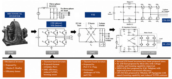
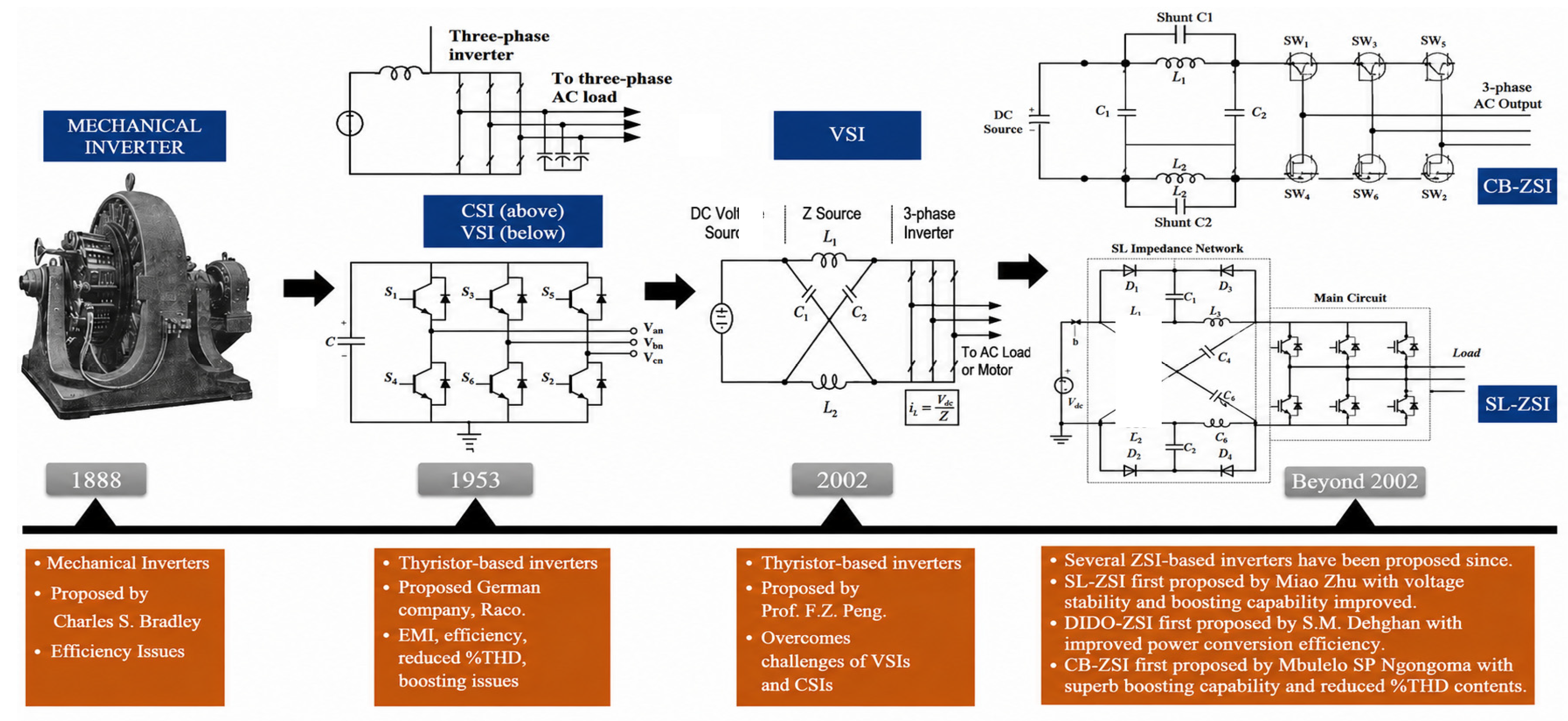
South Africa (SA) is one of the leading coal producers in the world (ranked seventh in the year 2021) and estimates project that the country has about 54 billion tons of coal left [3]. Factoring in the current rate of SA’s coal dissipation (plus the coal exports), estimates suggest these reserves will be depleted in the next 200 years, while environmental challenges will still be apparent during this time [4]. This implies that South Africa should already be exploring alternative energy sources to replace the current coal-fired power stations, and renewable energy, particularly photovoltaic (PV) energy, is increasingly becoming an integral part of SA’s smart grid. DC-AC converters are utilized to synchronize PV power systems into the national power grid. As a result, there has been an increasing focus on DC-AC converters. DC-AC converters have, therefore, evolved in several aspects of their conceptualization and operation over the years while improving efficiency, reliability, and power quality (to name a few) [5]. The 19th century was dominated by the early version of mechanical inverters. Figure 1 shows a typical mechanical inverter that was proposed by Charles S. in 1888, and it suffered from high losses and consequently low efficiency. The 20th century saw advancements in semiconductor technology and power-switching components such as bipolar junction transistors (BJTs), metal-oxide-semiconductor field-effect transistors (MOSFETs), thyristors, etc. This has allowed for the semi-conductor switch-based DC-AC inverters to be invented. Figure 1 shows that the Voltage-Source Inverter (VSI) and Current-Source Inverter (CSI) were introduced in the 1950s. The VSI and CSI generally outperformed the early mechanical inverters though they still had their own conceptual and practical limitations which include limited boosting range, susceptibility to shoot-through state caused by electromagnetic interference (EMI), and high total harmonic distortion content (THD) on the output power signals.
Figure 1.
Evolution of the inverter over the past years.
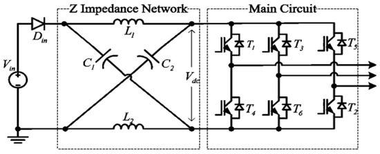
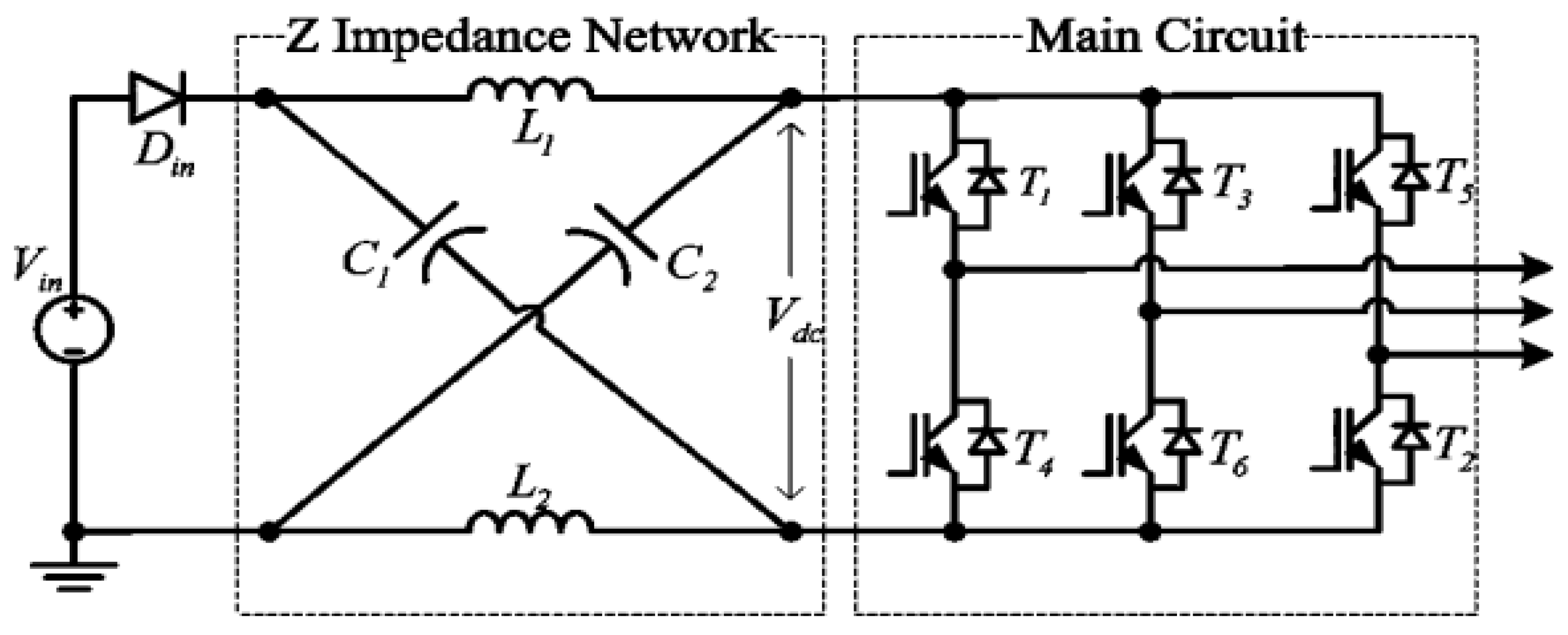
In 2002, Prof. F.Z. Penz proposed a Z-source inverter (ZSI)—refer to Figure 2—which also proved to overcome most of the shortcomings experienced with the VSI and CSI though itself has its own shortcomings too [6,7]. This inverter has a DC input source (Vin) connected in series with a diode (Din), an impedance network (comprising C1, C2, L1, and L2), and the main inverting circuit comprising power switches T1–T6. Though a ZSI is theoretically capable of buck-boosting in the range of zero to infinity (0-∞), the voltage stress (VS) and hence the %THD worsen as the boost factor (BF) is increased (or decreased) beyond unity [6,7].
Figure 2.
A Z-source inverter architecture [1].
As a result of this limitation and several others, researchers have proposed different ZSI-based topologies as solutions, such as the Switched-Inductance Z-Source inverter (SL-ZSI), as shown in Figure 1, and Quazi-Z-Source Inverter (q-ZSI).
The purpose of this paper is also to propose a different ZSI-based inverter topology with an improved boost factor and lower voltage stress across power electronic switches of the inverting stage. This ZSI-based inverter topology is called the Shunt Capacitor-Boosted Z-Source Inverter (SCB-ZSI). The SCB-ZSI has two additional capacitors on top of the original impedance network of a classical ZSI connected across the two inductors, L1 and L2. These extra shunt capacitors store additional energy and maintain residual voltage across the inductors L1 and L2 during the shoot-through switching state of the SCB-ZSI, which would not be the case in a classical ZSI. As a result, the boost factor of a CB-ZSI is higher than that of the classical ZSI and other ZSI-based topologies for the same Pulse Width Modulation (PWM) technique and it increases with the modulation index (m) and the magnitude of the shunt capacitor selected. Due to being able to achieve higher boost factors of the SCB-ZSI compared to other topologies for the same modulation index, the same is also true with the voltage stress across the power electronic switches (T1 to T6). The average voltage stress experienced by the power electronic switches on an SCB-ZSI topology is less than that experienced on other topologies for the same PWM technique and modulation index. When the shunt capacitance magnitude of an SCB-ZSI approaches zero, the SCB-ZSI topology converges to the traditional ZSI topology. What happens to the critical parameters of an SCB-ZSI (boost factor, voltage stress, %total harmonic distortion, etc.) when the shunt capacitance approaches infinity? The performance parameters of the SCB-ZSI continue to improve but reach a point when they plateau, that is, a further increase in the magnitude of the SCB-ZSI has minor or no impact on the key performance of the SCB-ZSI.
2. Related Work
Several authors have proposed different inverter topologies based on a traditional ZSI and each topology has displayed performance improvements relative to the traditional ZSI topology. This section discusses a few of these ZSI-based inverter topologies that have been proposed by different authors in the literature.
2.1. Switched-Inductor Z-Source Inverter (SL-ZSI)
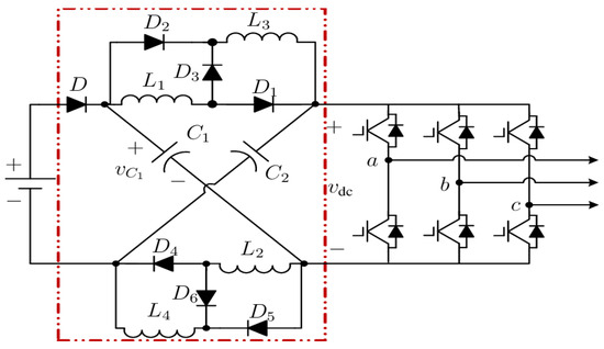
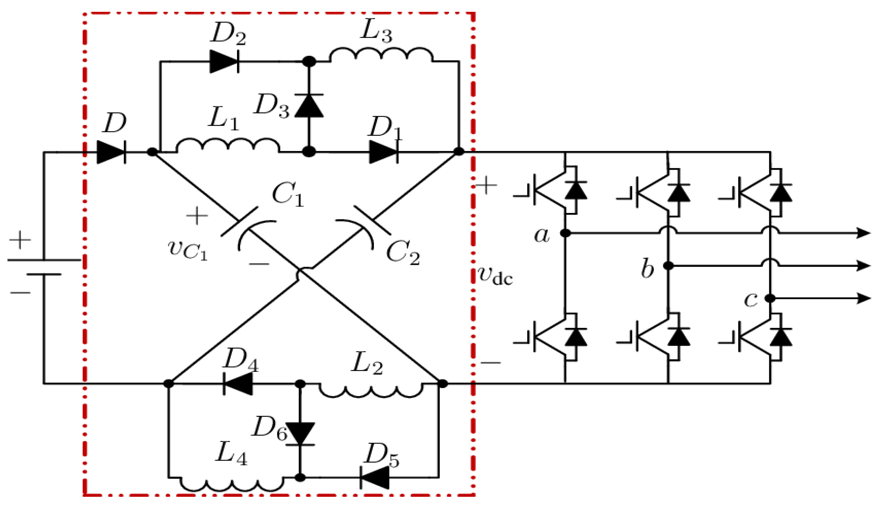
An SL-ZSI was proposed by Miao Zhu [8] and its architecture is shown in Figure 3. An SL-ZSI is made up of three main parts—the DC energy source, the SL-impedance network (marked in the red dashed box), and the inverting stage comprising six power switching devices (four in the case of a single-phase system) arranged in an H-bridge connection.
Figure 3.
Switched inductor Z-source inverter architecture [1].
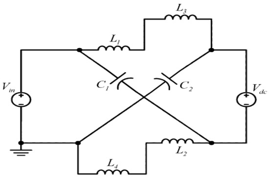
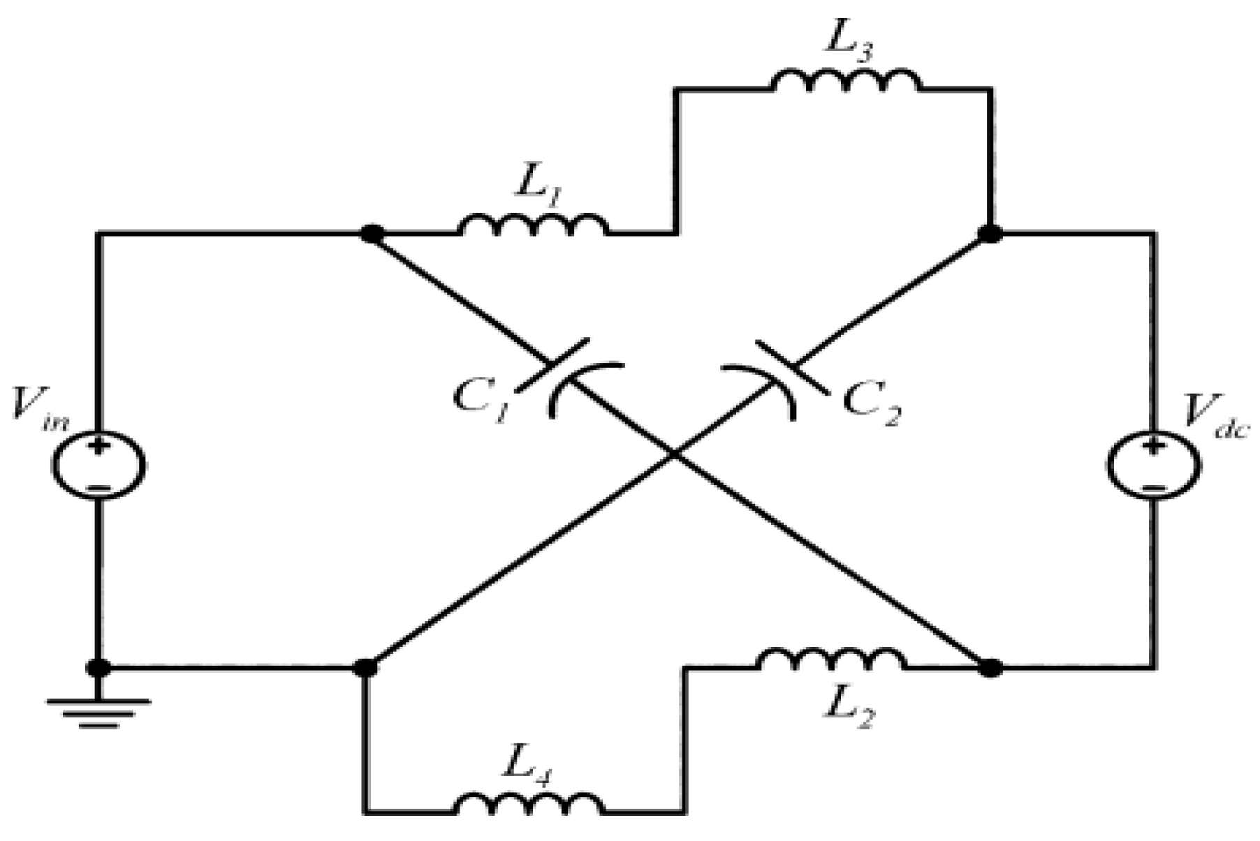
The major distinction between a traditional ZSI and an SL-ZSI is in the Z- and SL-impedance networks. The SL-impedance network has, in addition to the elements of a Z-impedance, two more inductors (L3 and L4) and six more diodes (D1–D6). The SL-ZSI, similar to the ZSI, can operate in two main states, viz., the shoot-through and the non-shoot-through states. Shoot-through occurs when one or more phase legs of the SL-ZSI are shorted [8]. The non-shoot-through occurs when the SL-ZSI is operating in one of the six active or two zero states [1,8,9,10,11]. The SL-impedance network is arranged such that Din, D3, and D6 are switched on while D1, D2, D4, and D5 are switched on during the non-shoot-through states. Figure 4 shows the non-shoot-through equivalent circuit of the SL-ZSI. In this state, the SL-ZSI is operating as a traditional ZSI with the inductors L1 and L3 as well as L2 and L4 connected in series. The energy stored in the inductors (during the shoot-though state) L1–L4 is transferred into the main inverting circuit towards the load while the capacitors C1 and C2 are charged during the same state.
Figure 4.
Non-shoot-through equivalent circuit of an SL-ZSI.
In the shoot-through state, Din, D3, and D6 are switched off while D1, D2, D4, and D5 are switched on. This turns inductors L1 and L3 as well as L2 and L4 into parallel combinations and the corresponding equivalent circuit of an SL-ZSI is shown in Figure 5. During this state, the DC source is disconnected from the SL-ZSI, and the capacitors C1 and C2 discharge through inductors L1 and L3 as well as L2 and L4 respectively.
Figure 5.
Shoot-through equivalent circuit of an SL-ZSI.
The SL-ZSI proved to have better boosting capabilities and lower voltage stresses (and hence lower %THD) on the power electronics components relative to the traditional ZSI.
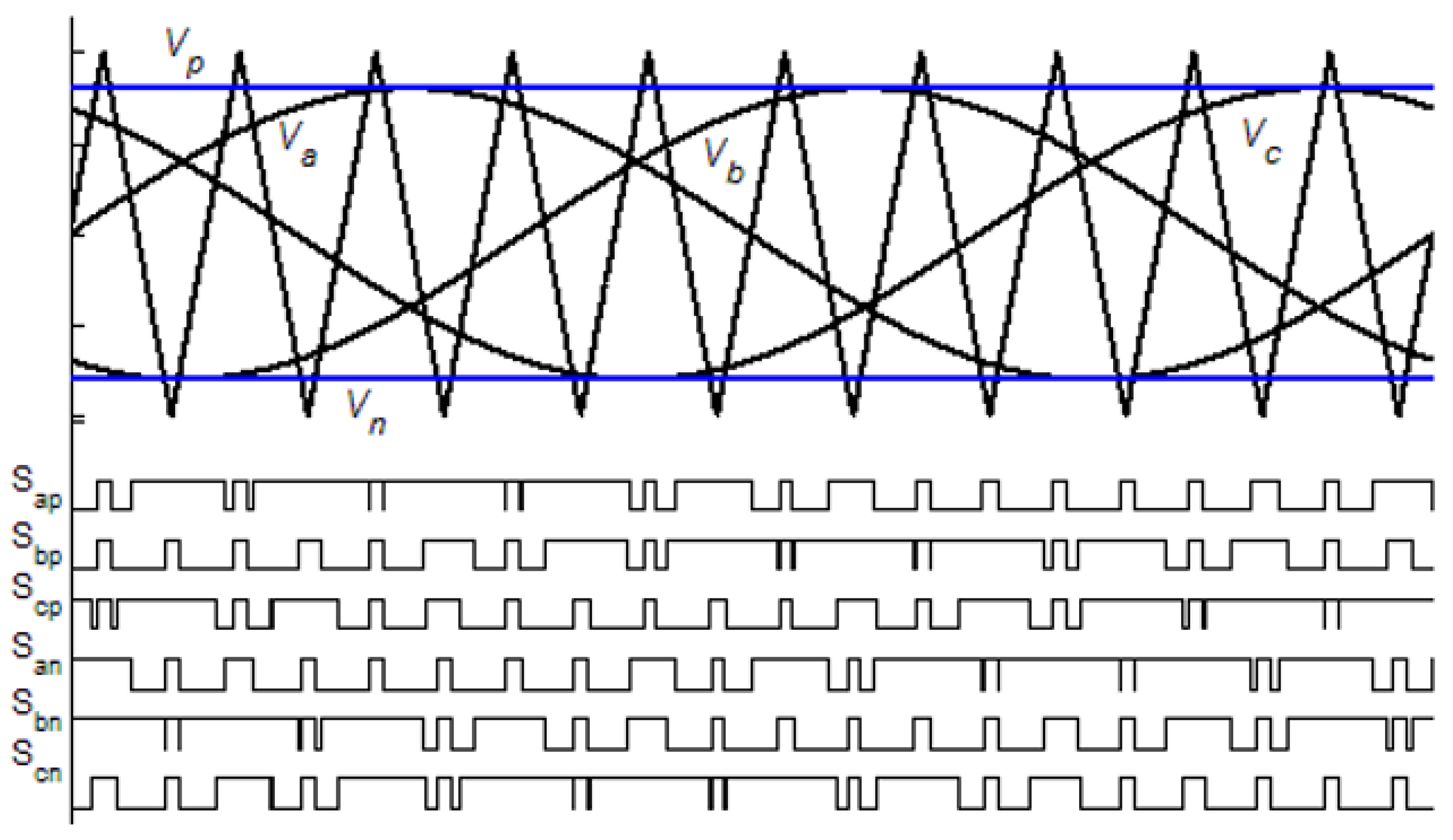
Equations (1) and (2) show the boost factor of the traditional ZSI and SL-ZSI respectively where D0 is the shoot-through duty ratio. The shoot-through duty ratio is the ratio of the shoot-through time (T0) to the switching period (T) of the main circuit’s Pulse Width Modulation (PWM) generator. Several PWM schemes have been proposed in the literature and their strengths and weaknesses have been discussed; however, the simple, constant, and maximum boost are the three most cited. Figure 6 shows how the PWM signals for switches S1–S6 are generated where Va, Vb, and Vc are the three-phase fundamental signals, Vp and Vn are modulation signals and the triangular wave is the switching carrier signal.
Figure 6.
The simple boost PWM scheme [8].
The shoot-through state (for all three phases) occurs when the carrier signal is greater than the positive modulating signal Vp and when it is less than the negative modulating signal Vn. The zero state occurs for a specific phase (a, b, or c) when its fundamental wave is less than the switching carrier signal. Similarly, the active state occurs for a specific phase (a, b, or c) when its fundamental wave is greater than the switching carrier signal. The ratio between the amplitude of the positive modulating signal and the amplitude of the switching carrier signal is termed the modulation index (MI). The voltage gain (VG) of the SL-ZSI is then defined as the product of the modulation index and the boost factor as depicted in Equation (3) [12,13].
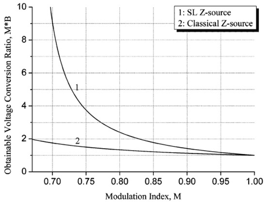
Figure 7 shows the relationship between the modulation index and the voltage gain for the SL-ZSI as well as the traditional ZSI. It can be seen from this figure that the voltage gain factor of an SL-ZSI is always greater or equal to that of a traditional ZSI across all the values of a modulation index in the allowable range. Therefore, an SL-ZSI is one of the ZSI topologies that proved to be successful in improving the performance of a classical ZSI topology.
Figure 7.
Modulation-gain characteristic for an SL-ZSI (under simple boost PWM control) [4].
2.2. Other ZSI-Based Inverter Found in the Literature
Several other inverter topologies based on a classical ZSI have been proposed in the literature and this section presents them summarily by looking at the most critical distinctions amongst them, as shown in Table 1.
Table 1.
Summary of other ZSI-based inverter topologies found in the literature.
Several other ZSI-based topologies can be found in the literature; however, this section focused on a few key points. The next section will present the conceptualization and mathematical modeling of yet another ZSI-based topology that is proposed by this research paper.
3. Materials and Methods
The purpose of this section is to conceptualize and mathematically model a different inverter topology called Shunt Capacitor-Boosted Z-Source Inverter (SCB-ZSI). A simple boost PWM scheme will then be designed to test the performance of an SCB-ZSI in the next section. MATLAB Simulink environment will be used to simulate and sample the performance results of this proposed inverter.
3.1. Conceptualization of an SCB-ZSI
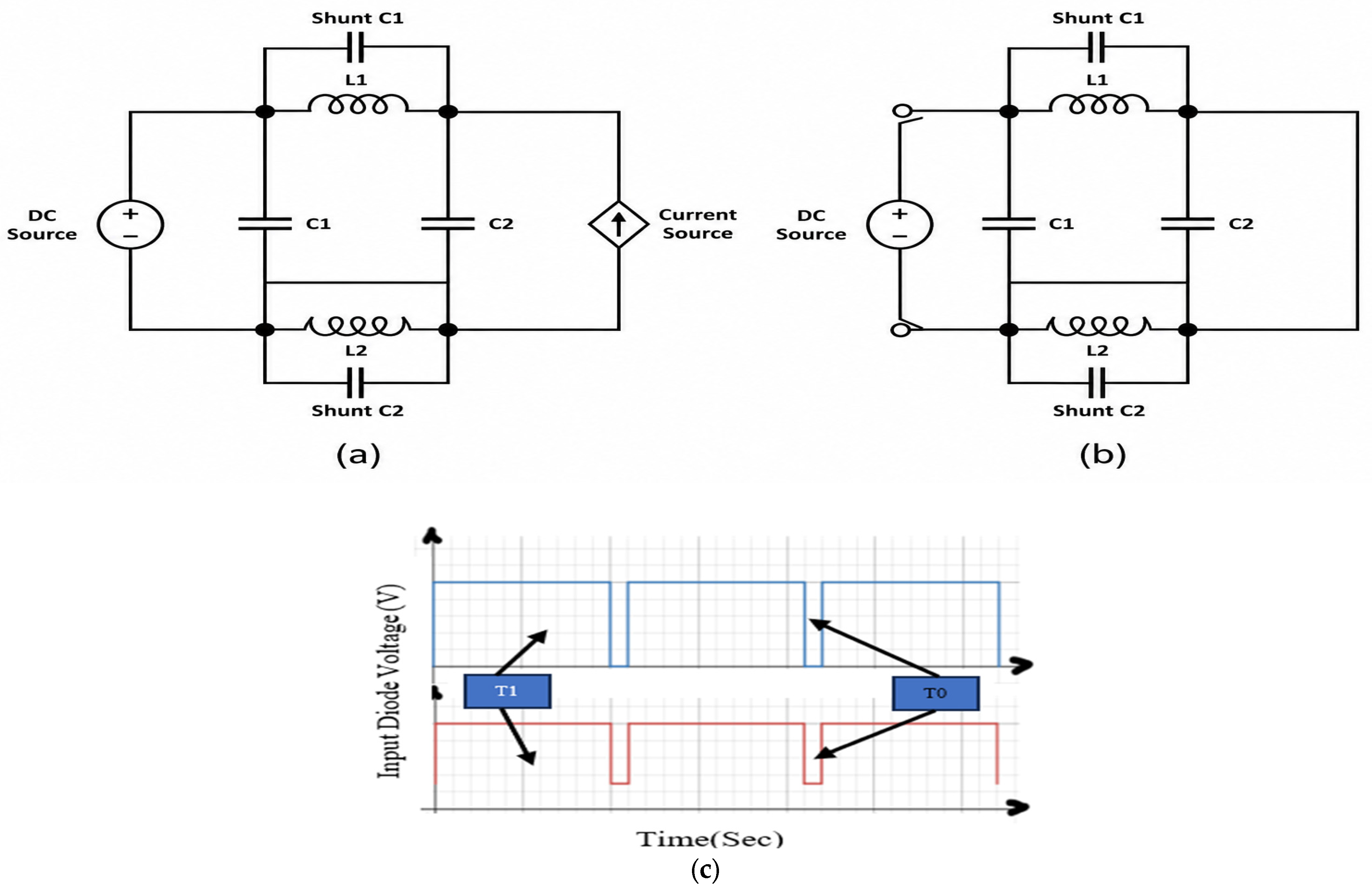
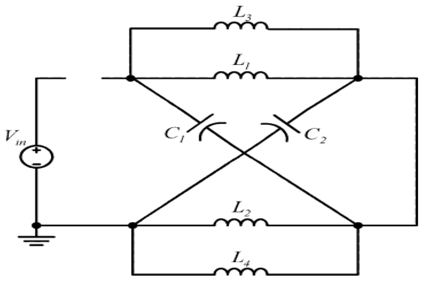
Figure 8 shows the architecture of the proposed SCB-ZSI. All other parts of a traditional ZSI are retained except the appending of parallel capacitors, shunt C1 and shunt C2, across the inductors L1 and L2 respectively. The SCB-ZSI operates in two main states, the shoot-through and non-shoot-through state. During the non-shoot-through state, the DC source charges all the capacitors in the SCB-ZSI including the shunt capacitors (only C1 and C2 charges during this state in the classical ZSI). The equivalent circuit of an SCB-ZSI when operating in this state is shown in Figure 9a. During the non-shoot-through state, the input diode (Din) is turned on and the main inverting circuit is seen as an AC-current source looking from the load side. During the shoot-through state, the DC source is disconnected from the SCB-ZSI as Din is turned off, and the energy stored in the capacitors C1 and C2 as well as the shunt capacitors is discharged through the inductors L1 and L2 toward the load. The equivalent circuit of an SCB-ZSI when operating in the shoot-through state is shown in Figure 9b. The average voltage across the inductors L1 and L2 is zero under steady-state conditions for a traditional ZSI; however, it is no longer the case for CB-ZSI because the shunt capacitors maintain a residual voltage across these inductors even at steady-state. The SCB-ZSI, therefore, has the following two main advantages over the traditional ZSI:
- An SCB-ZSI has a greater boost factor relative to the traditional ZSI for the same modulation index.
- An SCB-ZSI has a lower voltage stress across the switching devices relative to the traditional ZSI for the same gain factor.
Figure 8.
The SCB-ZSI architecture.
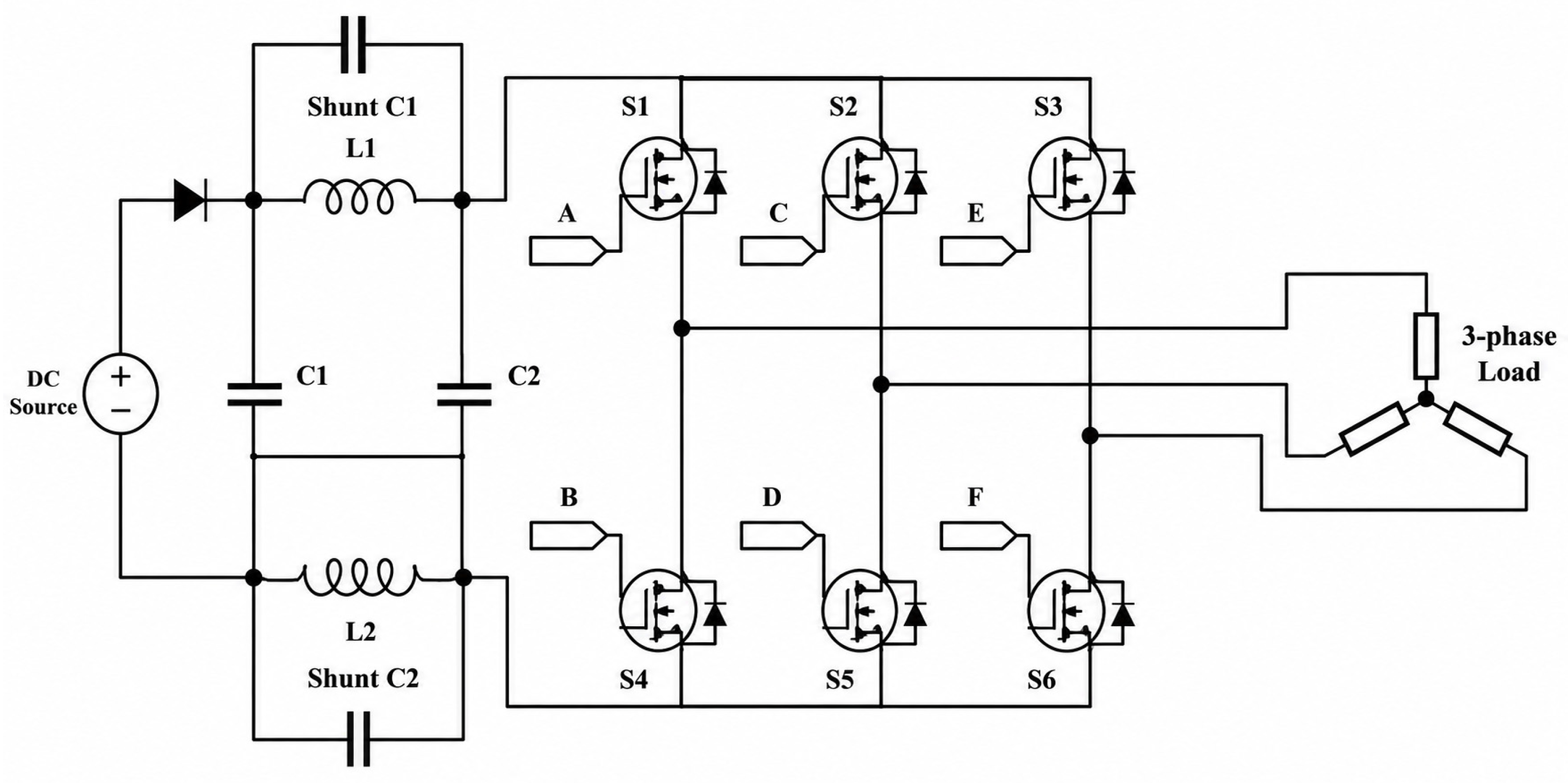
Figure 9.
(a) Non-shoot-through, (b) shoot-through equivalent circuits of an SCB-ZSI and (c) operational waveform of the inductor during T0 and T1 for a ZSI vs. SCB-ZSI.
3.2. Mathematical Modeling of an SCB-ZSI
For simplicity and easier analysis of this SCB-ZSI architecture, the symmetrical conditions on the impedance network are assumed. This implies that the voltages across the impedance network’s capacitors and inductors, as well as the shunt capacitors, are equal as depicted by Equation (4) where Vl, Vc, and Vs are the voltages across the impedance network’s capacitors and inductors as well as the shunt capacitors respectively.
- When the SCB-ZSI is operating at a shoot-through state, the voltages across the impedance network’s capacitors and inductors as well as the shunt capacitors are equal while the voltage immediately after the impedance network as seen from the main inverting circuit (VDC-bus) is zero, as depicted by Equation (5) [16,17]:
- When the SCB-ZSI is operating at a shoot-through state, the voltage across the inductors and shunt capacitors is equal; however, they are both no longer equal to the main capacitor voltages. As a result, the DC bus voltage is no longer zero and can be derived using Kirchoff’s voltage law, as shown in Equation (6) [8,9,15,16,17]:
The average steady-state voltage-time product across the impedance network’s inductors is approximately zero in the traditional ZSI but no longer the case for the SCB-ZSI because of the residual voltage maintained by the shunt capacitors, as previously stated. The average voltage-time product for the SCB-ZSI is now defined by Equation (7) where Vl-shoot-through and Vl-non-shoot-through are the inductors’ voltages during shoot-through (T0) and non-shoot-through states (T1):
The RHS of Equation (7) is represented in terms of the shoot-through time (T0), non-shoot-through time (T1), and capacitor voltage (Vc). Then, rearranging the equation yields the voltage ratio between the capacitor and the DC source depicted in Equation (8) [16,18].
The period magnitude is constant and independent of the size of the shunt capacitors utilized, and hence the proportional factors k1 and k2. These dimensionless factors range from 0 to 1 and they only impact the distribution of the shoot-through and non-shoot-through times while the switching period remains constant. Therefore, substituting Equation (8) into Equation (6), the main boost factor of an SCB-ZSI is defined (refer to Equation (9)).
Therefore, it can be seen that increasing the value of k2 increases the boost factor of the SCB-ZSI. The k2 value for a traditional ZSI is zero. By looking at Equation (9) it can be seen that an SCB-ZSI has a greater boosting capability than a traditional ZSI. The coming section designs a simple boost PWM controller for the testing of this SCB-ZSI MATLAB Simulink.
3.3. Design of a Simple Boost PWM Control Scheme for the SCB-ZSI
Three important functions are used to design the simple boost PWM generator. They are the three-phase fundamental function (refer to Equation (10)), the triangular switching carrier function (refer to Equation (10)), and the modulating constant functions (refer to Equation (11)).
A set of secondary Boolean variables (VAR1–VAR5) has to be defined to fully define all the switching states of an SCB-ZSI. These variables can either be 0 or 1 and they each carry the crucial information of the instantaneous relationship between two signals (. These variables are mathematically defined in Equations (13)–(17).
When VAR1 is high (1) at an instantaneous time t, it implies that the signal of phase A (Va(t)) is greater than the signal of phase B (Vb(t)); if VAR1 is low (0), then the opposite is true. When VAR2 is high (1) at an instantaneous time t, it implies that the signal of phase B (Vb(t)) is greater than the signal of phase C (Vc(t)); if VAR2 is low (0), then the opposite is true. When VAR3 is high (1) at an instantaneous time t, it implies that the signal of phase C (Vc(t)) is greater than the signal of phase A (Va(t)); if VAR3 is low (0), then the opposite is true. When VAR4 is high (1) at an instantaneous time t, it implies that the carrier wave (Vcarrier(t)) is greater than the positive constant wave (a); if VAR4 is low (0), then the opposite is true. When VAR5 is high (1) at an instantaneous time t, it implies that the carrier wave (Vcarrier(t)) is less than the negative constant wave (-a); if VAR5 is low (0), then the opposite is true. Table 2 shows the definition of all the switching states of an SCB-ZSI using the previously defined secondary variables.
Table 2.
The switching states of an SCB-ZSI under simple boost PWM scheme.
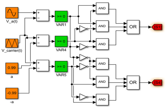
In Table 2, all the high (1) states with asterisks are shoot-through, all those that are high (1) but without asterisks are active non-shoot-through and all those that are low (0) are zero non-shoot-through states. The Sum of Products (or Product of Sums) method (SOPs) can then be used to formulate a digital PWM control circuit for switching devices S1 to S6. However, this section will only show the PWM control circuit for phase leg A (S1 and S4) because those of other phases are phase-shifted replicas of phase A. Figure 10 shows the simple boost PWM signal generator for the SCB-ZSI. The orange highlighted blocks are the primary variables (Equations (10)–(12)), the green highlighted blocks are the secondary variables (Equations (13), (15) and (16)) and the red highlighted blocks are the PWM switching signals for S1 and S4. Up to this point, the SCB-ZSI has been conceptualized and mathematically modeled, and the simple boost PWM control scheme has been designed to test the proposed model. The next section will cover the testing results of the SCB-ZSI in MATLAB Simulink.
Figure 10.
Simple boost signal generator for the SCB-ZSI.
4. Results
The SCB-ZSI was simulated on the MATLAB Simulink R2022a version under the control of a simple boost PWM scheme. Three key parameters were observed during the testing of an SCB-ZSI, namely the boost factor (BF), the voltage stress (VS) across the switching components, and the percentage of total harmonic distortion (%THD). These key parameters of an SCB-ZSI were compared to those of the traditional ZSI to see the level of improvement as suggested by mathematical modeling. The input DC voltage ranged between 200 and 500 in steps of 100, while the modulation index (MI) ranged between 0.65 and 0.95 in 0.1 steps. Table 3 and Table 4 show the recorded operational data for a ZSI and an SCB-ZSI.
Table 3.
Classical ZSI operational data under the simple boost PWM control technique.
- The voltage stress on the power electronic switches (see Figure 11a), the percentage of total harmonic distortion (see Figure 11b), the boost and the gain factors are only dependent on one external factor (excluding the intrinsic design factors of the switch)—the modulation index. All the parameters show an inverse relationship with the modulation index.
Figure 11.
(a) Average VS vs. MI; and (b) average %THD vs. MI.
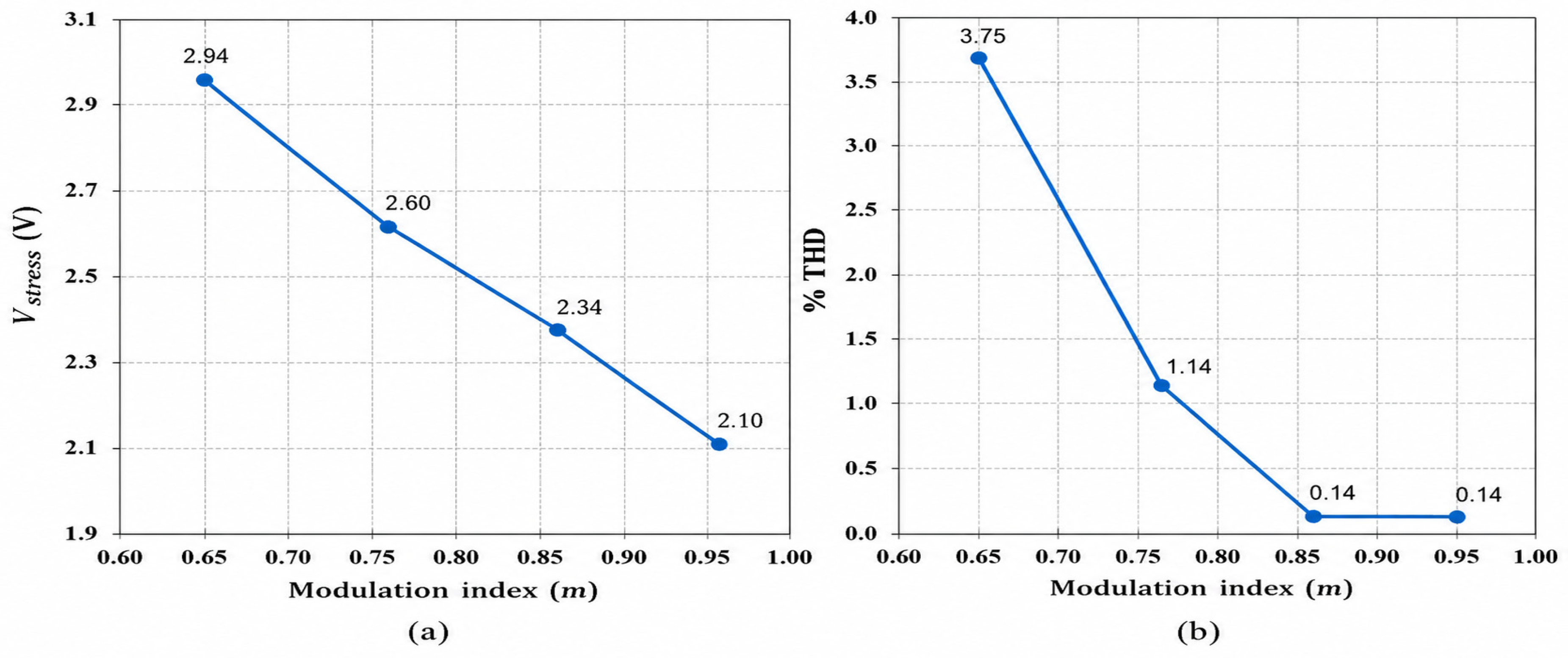
Figure 12.
(a) Average VOut vs. VI; and (b) average VD vs. Vin.
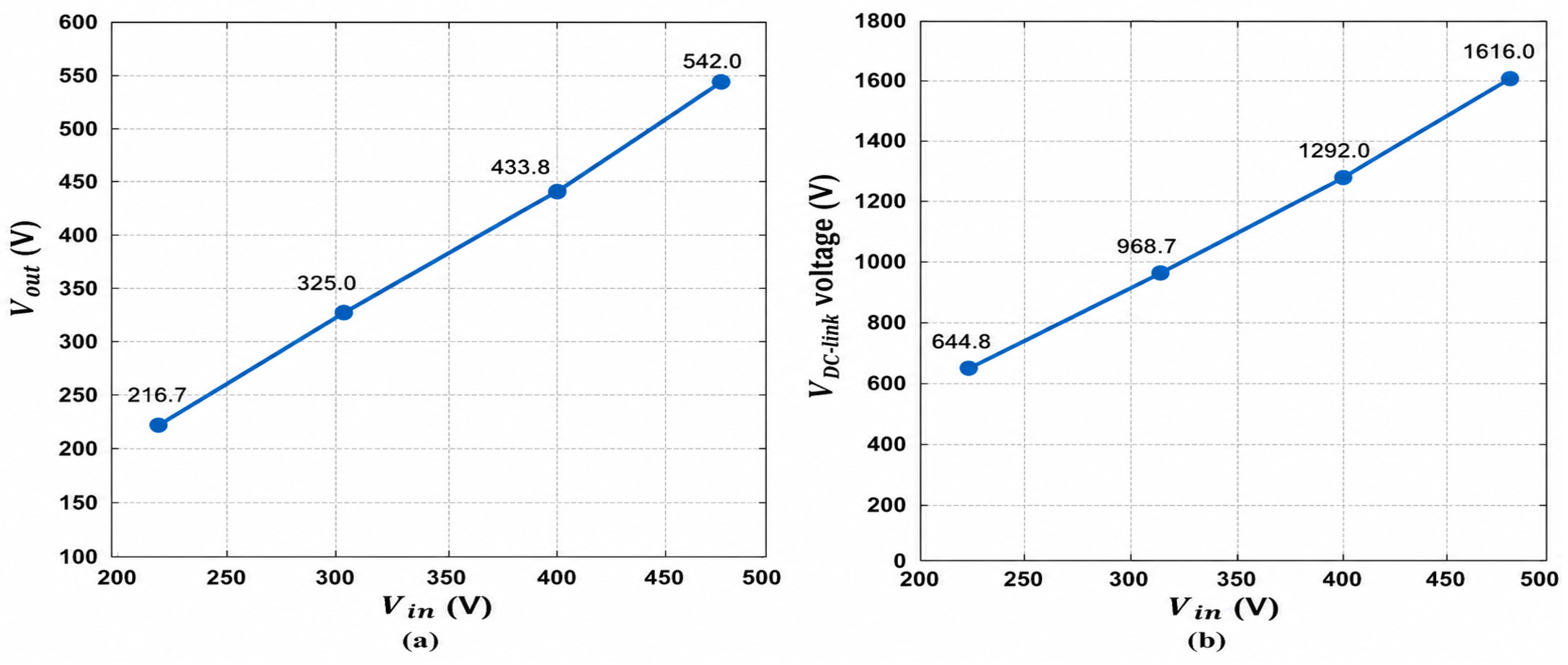
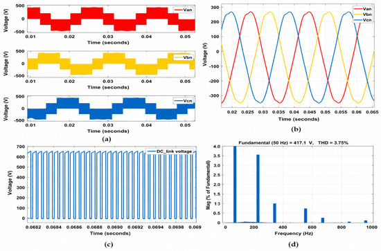
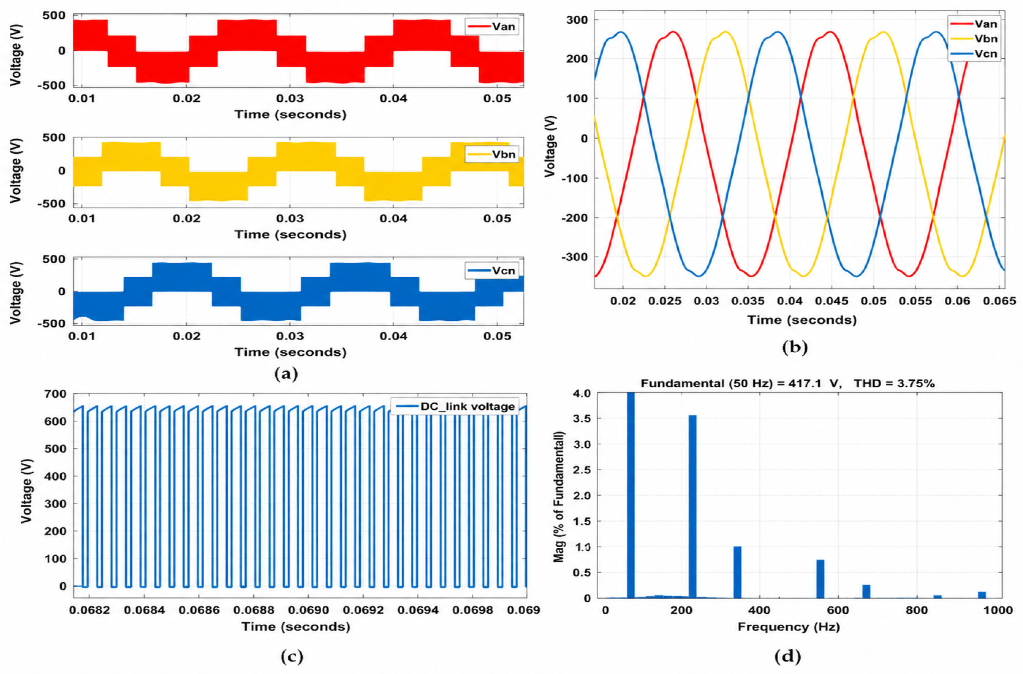
Figure 13 shows the unfiltered output phase voltage (Figure 13a), the filtered output phase voltage (Figure 13b), the DC-link voltage (Figure 13c), and the % of total harmonic distortion (Figure 13d) of a classical ZSI sampled when the input voltage was set at 200V and the modulation index at 0.65.
Figure 13.
(a) Unfiltered output phase voltage vs. time; (b) filtered output phase voltage vs. time (c) DC-link voltage vs. time; and (d) %total harmonic distortion vs. frequency for a classical.
The same data (as that of ZSI in Table 3) were extracted from an SCB-ZSI to compare its performance to that of a classical ZSI. These operational data are outlined in Table 4. It is also important to note that these data were collected when the SCB-ZSI was also under the control of the simple boost control technique and that the shunt capacitor C1 and C2 were set to 1% the magnitude of the original Z-impedance network capacitors. Again, the same relationships were observed between key performance parameters of the SCB-ZSI as those of a classical ZSI, with the major difference being the shift in the SCB-ZSI curves relative to those shown in Figure 11, by a constant factor either up or down, depending on the parameters being considered at a time.
Table 4.
SCB-ZSI operational data under the simple boost PWM control.
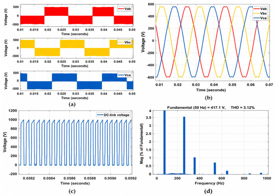
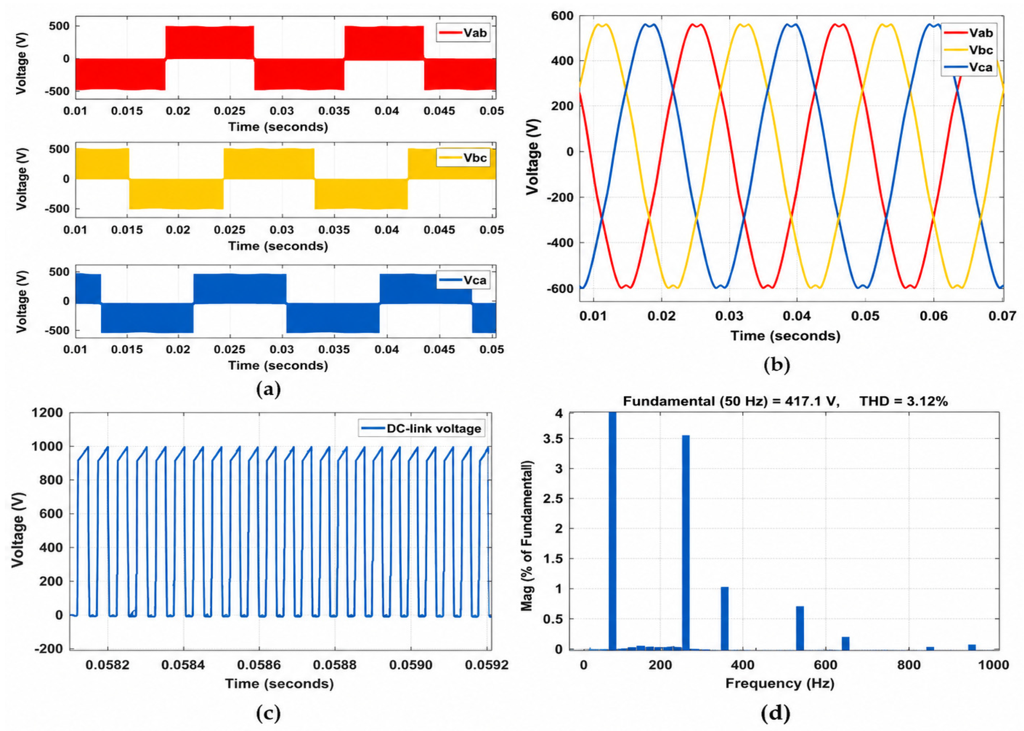
Again, Figure 14 shows the unfiltered output phase voltage (Figure 14a), the filtered output phase voltage (Figure 14b), the DC-link voltage (Figure 14c), and the percentage of total harmonic distortion (Figure 14d) of an SCB-ZSI sampled when the input voltage was set at 200V and the modulation index at 0.65.
Figure 14.
(a) Unfiltered output phase voltage vs. time; (b) filtered output phase voltage vs. time (c) DClink voltage vs. time; and (d) %total harmonic distortion vs. frequency for an SCBZSI.
5. Discussion
One can deduct various key factors from examining the operational data of an SCB-ZSI and that of a classical ZSI. Those are:
- The boost factor and hence the gain factor of the SCB-ZSI are always greater compared to that of a classical ZSI for the same input voltage and modulation index. This concurs with the theoretical mathematical modeling of the SCB-ZSI.
The above inequality shows that the boost factor of an SCB-ZSI will always be greater than the boost factor of a classical ZSI for values of k2 such that this constant is greater than zero and the term ‘2(1 + k_2) D_0’ ranges between 0 and 1. This will always be the case when non-zero or finite shunt capacitors C1 and C2 are selected.
- The second observation made was that the voltage stress across the switching components of an SCB-ZSI is less than average compared to that of a classical ZSI for the same input voltage and modulation index. This directly influences the switching efficiency of the semiconductor materials found in these switches which tend to heat up under excessive voltage stress. Therefore, less voltage stress implies less switching loss, less distortion to the output signals, and hence more power conversion efficiency and good quality on the power signals.
- The third observation was that the average percentage of total harmonics distortion on the SCB-ZSI has output voltage is less than that of the classical ZSI. This implies less strain on the filtering circuits and ease of connecting renewable energy sources to the power grid if the harmonics content of this inverter is reduced.
- The SCB-ZSI, just like the ZSI, is immune against the damage caused by the electromagnetic interference (EMI), which is apparent with the most conventional inverter topologies like the CSI and the VSI.
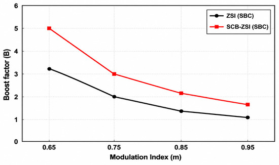
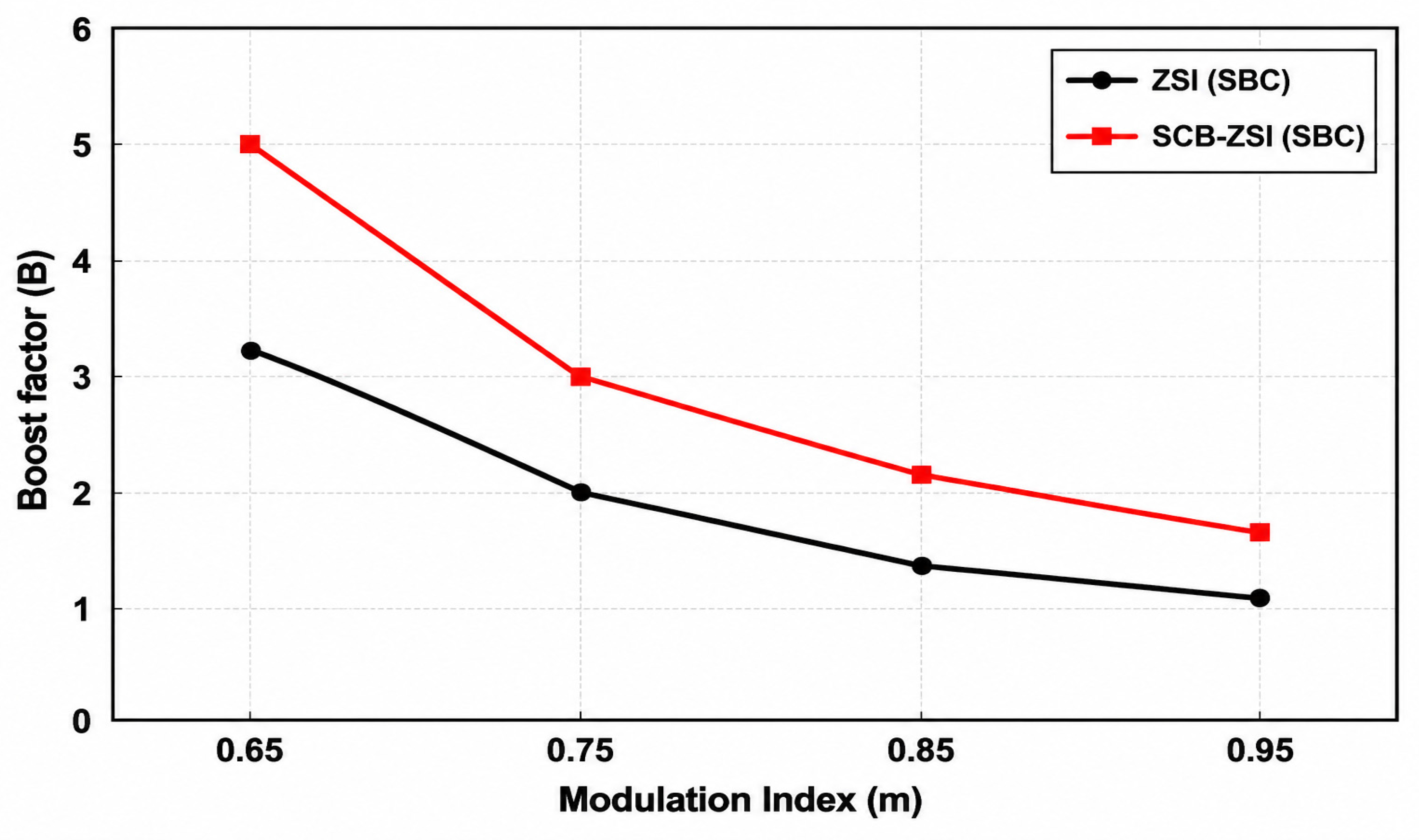
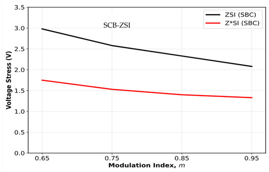
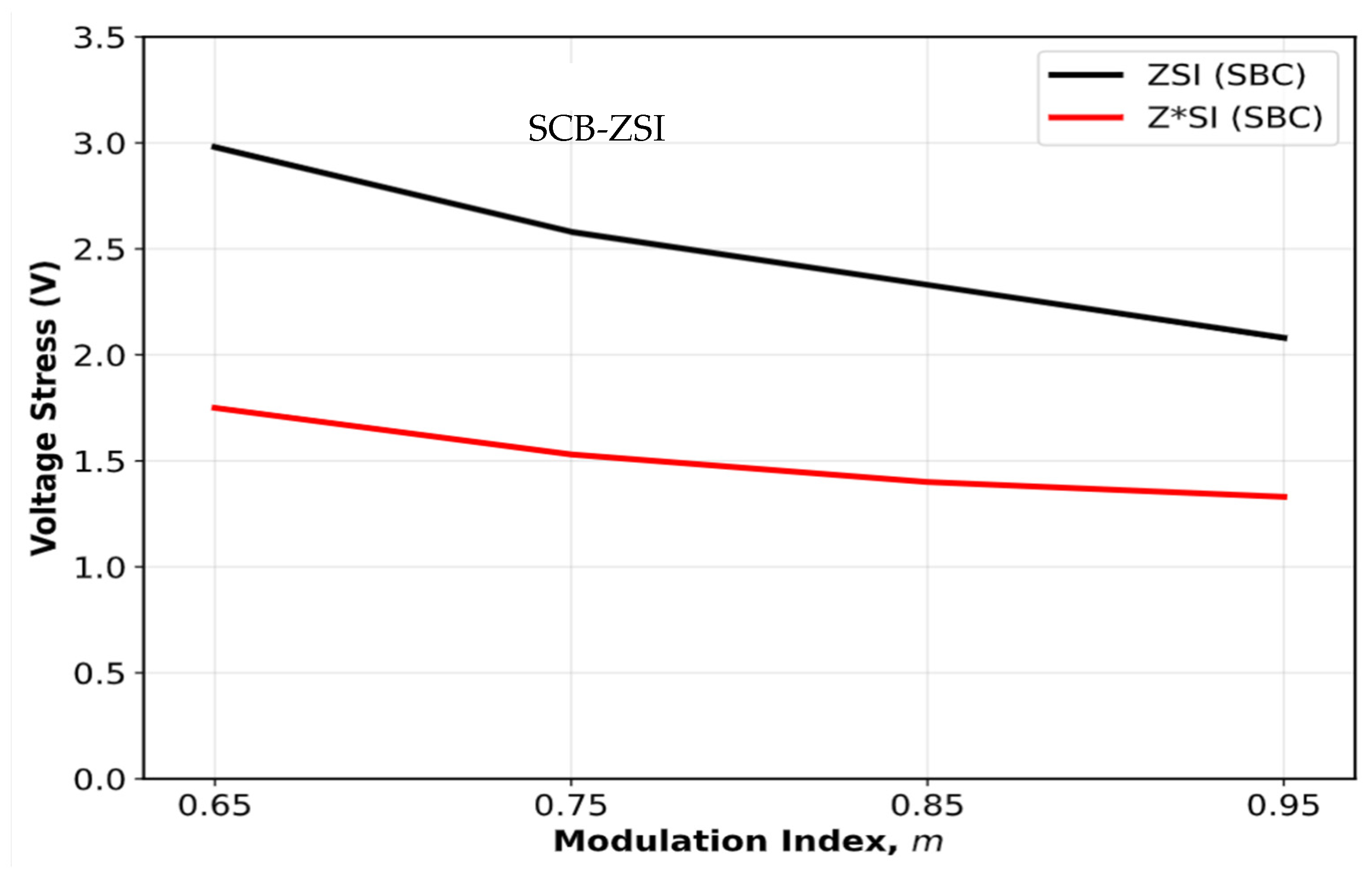
Figure 15 and Figure 16 show that the SCB-ZSI has better boosting capability relative to the traditional ZSI and it incurs less stress on the switching components relative to the traditional ZSI. This is a crucial achievement, especially in renewable energy applications, such as PV power systems, where a much higher initial voltage boost is required for tying a PV system to a power grid. This also implies that the SCB-ZSI allows the power electronics switching components to operate more efficiently compared to the traditional ZSI, which improves the overall efficiency and the power quality of the SCB-ZSI relative to the traditional ZSI.
Figure 15.
The boost factor of SCB-ZSI vs. ZSI over different modulation indexes.
Figure 16.
The switch voltage stress of SCB-ZSI vs. ZSI over different modulation indexes.
6. Conclusions
The SCB-ZSI is one of the promising ZSI-based topologies that has proved to outperform the traditional ZSI topology in the boosting capability and the voltage stress incurred across the power electronic switching devices areas. The simulation test results showed that the selection of shunt capacitors of a ZSI at 1% of those of the original ZSI improves the boost factor by 56% and reduces the switch voltage stress ration by 40% on an SCB-ZSI for the same set of input parameters. However, there is still more work that needs to be done on this newly proposed inverter topology before it can be applied in industrial applications. The %THD performance of the SCB-ZSI still has to be investigated. The standard design algorithm for the shunt capacitor still needs to be developed more. The limits of the shunt capacitors still need to be established as it may be a tedious task to select the optimum ratings of the shunt capacitors using trial and error method. When the shunt capacitors approach zero, the SCB-ZSI becomes the traditional ZSI. When the shunt capacitance approaches infinity, the SCB-ZSI gains on the traditional ZSI plateaus. Therefore, a guide has to be established that determines the best or optimum setting of the shunt capacitors’ magnitudes at different design requirements. The SCB-ZSI was tested on the simple boost PWM scheme; the topology still needs to be explored using other PWM schemes. The SCB-ZSI was evaluated using the traditional ZSI; it is still to be evaluated against other ZSI-based topologies. However, the SCB-ZSI remains a promising DC-AC inverter topology that comes with more performance capabilities compared to the traditional ZSI.
Author Contributions
Conceptualization, M.S.P.N. and Z.P.K.; methodology, M.S.P.N.; software, M.S.P.N.; validation, M.S.P.N., and Z.P.K.; formal analysis, M.S.P.N.; investigation, M.S.P.N.; resources, M.S.P.N.; data curation, M.S.P.N.; writing—original draft preparation, M.S.P.N.; writing—review and editing, M.S.P.N.; visualization, M.S.P.N. All authors have read and agreed to the published version of the manuscript.
Funding
This research received no external funding.
Institutional Review Board Statement
Not applicable.
Informed Consent Statement
Not applicable.
Data Availability Statement
Any additional data relating to this study is available upon request.
Conflicts of Interest
The authors declare no conflict of interest.
References
- Choudhury, A.; Pillay, P.; Williamson, S.S. Comparative analysis between two-level and three-level DC/AC electric vehicle traction inverters using a novel DC-link voltage balancing algorithm. IEEE J. Emerg. Sel. Top. Power Electron. 2014, 2, 529–540. [Google Scholar] [CrossRef] [Scilit]
- Mohammed, S.A.Q.; Jung, J.-W. A state-of-the-art review on soft-switching techniques for DC–DC, DC–AC, AC–DC, and AC–AC power converters. IEEE Trans. Ind. Inform. 2021, 17, 6569–6582. [Google Scholar] [CrossRef] [Scilit]
- Akinbami, O.M.; Oke, S.R.; Bodunrin, M.O. The state of renewable energy development in South Africa: An overview. Alex. Eng. J. 2021, 60, 5077–5093. [Google Scholar] [CrossRef] [Scilit]
- Adewole, K.S.; Akintola, A.; Salihu, S.A.; Faruk, N.; Jimoh, R.G. Hybrid rule-based model for phishing URLs detection. In International Conference for Emerging Technologies in Computing; Springer: Berlin/Heidelberg, Germany, 2019. [Google Scholar]
- Wang, X.; Li, Y.W.; Blaabjerg, F.; Loh, P.C. Virtual-impedance-based control for voltage-source and current-source converters. IEEE Trans. Power Electron. 2014, 30, 7019–7037. [Google Scholar]
- Ngongoma, M.S.P.; Davidson, I.E.; Agee, J.T. Improvement of a Three-Phase Z-Source Inverter Performance. In 2023 31st Southern African Universities Power Engineering Conference (SAUPEC); IEEE: Piscataway, NJ, USA, 2023. [Google Scholar]
- Ngongoma, M.S.P. Impact of Different Pulse Width Modulation (PWM) Techniques on the Performance of a Three Phase Z-Source Inverter (ZSI). Master’s Theses, University of KwaZulu-Natal, Durban, South Africa, 2019. [Google Scholar]
- Zhu, M.; Yu, K.; Luo, F.L. Switched inductor Z-source inverter. IEEE Trans. Power Electron. 2010, 25, 2150–2158. [Google Scholar] [CrossRef] [Scilit]
- Berg, M.; Roinila, T. Dynamic Effect of Input-Voltage Feedforward in Three-Phase Grid-Forming Inverters. Energies 2020, 13, 2923. [Google Scholar] [CrossRef] [Scilit]
- Lu, X.; Wang, J.; Guerrero, J.M.; Zhao, D. Virtual-impedance-based fault current limiters for inverter dominated AC microgrids. IEEE Trans. Smart Grid 2016, 9, 1599–1612. [Google Scholar] [CrossRef] [Scilit]
- Peng, F.Z. Z-source inverter. IEEE Trans. Ind. Appl. 2003, 39, 504–510. [Google Scholar] [CrossRef] [Scilit]
- Siwakoti, Y.P.; Peng, F.Z.; Blaabjerg, F.; Loh, P.C.; Town, G.E. Impedance-Source Networks for Electric Power Conversion Part I: A Topological Review. IEEE Trans. Power Electron. 2015, 30, 699–716. [Google Scholar] [CrossRef] [Scilit]
- Barath, J.G.N.; Soundarrajan, A.; Stepenko, S.; Padmanaban, S.; Prystupa, A.; Bolotov, M. Review of Extended Boost qZSI Topologies for Single Phase Applications. In Proceedings of the 2019 IEEE 60th International Scientific Conference on Power and Electrical Engineering of Riga Technical University (RTUCON), Riga, Latvia, 7–9 October 2019; pp. 1–8. [Google Scholar] [CrossRef] [Scilit]
- Stepenko, S.; Husev, O.; Vinnikov, D.; Roncero-Clemente, C.; Pires Pimentel, S.; Santasheva, E. Experimental comparison of two-level full-SiC and three-level Si–SiC quasi-Z-source inverters for PV applications. Energies 2019, 12, 2509. [Google Scholar] [CrossRef] [Scilit]
- Kannan, P. Quazi Z Source Network Based Three Phase Inverter Using Space Vector PWM Technique. Int. J. Emerg. Technol. Innov. Eng. 2019, 5, 7. [Google Scholar]
- Nguyen, M.K.; Lim, Y.-C.; Choi, J.-H.; Choi, Y.-O. Trans-switched boost inverters. IET Power Electron. 2016, 9, 1065–1073. [Google Scholar] [CrossRef] [Scilit]
- Ahmad, A.; Singh, R.K.; Beig, A.R. Switched-capacitor based modified extended high gain switched boost Z-source inverters. IEEE Access 2019, 7, 179918–179928. [Google Scholar] [CrossRef] [Scilit]
- Subudhi, P.S.; Krithiga, S. Topological study of derived converters review. In 2019 2nd International Conference on Power and Embedded Drive Control (ICPEDC); IEEE: Piscataway, NJ, USA, 2019. [Google Scholar]

Disclaimer/Publisher’s Note: The statements, opinions and data contained in all publications are solely those of the individual author(s) and contributor(s) and not of MDPI and/or the editor(s). MDPI and/or the editor(s) disclaim responsibility for any injury to people or property resulting from any ideas, methods, instructions or products referred to in the content. |
© 2026 by the authors. Licensee MDPI, Basel, Switzerland. This article is an open access article distributed under the terms and conditions of the Creative Commons Attribution (CC BY) license.