


Abstract
The increasing penetration of renewable technologies, particularly photovoltaic (PV) and fuel cell (FC) systems, into microgrid networks has created new challenges in maintaining voltage stability, harmonic performance, and overall power quality. This study presents a comparative evaluation of two modulation and control strategies, which are a Simple Boost Control (SBC) and Space Vector Modulation (SVM). The system is modeled and simulated under standard test conditions (STC) as well as dynamic fluctuations in irradiance to evaluate the inverter performance, total harmonic distortion (THD), and DC-link voltage stability. Simulation findings indicate that although SBC provides structural simplicity and dependable voltage enhancement, the SVM approach delivers greater harmonic mitigation, more seamless inverter performance, and improved voltage utilisation in variable conditions. The results enhance the optimisation of power electronic control systems for renewable energy microgrids, facilitating steady and efficient operation in accordance with South Africa’s green energy goals.
1. Introduction
Single-stage DC-AC power converters have rapidly evolved in recent years for distributed microgrids to replace the traditional two-stage architecture, which consists of a front-end DC-DC boost converter and an output voltage source inverter, due to a growing global demand for sustainable and reliable energy systems. Numerous research initiatives have been initiated on the impedance source inverter (ZSI) to enhance its performance from many aspects, including overall gain, voltage stresses across different components, and the continuity of input current. This development encompasses several enhancements and alterations implemented in the ZSI topology, including its modulation, leading to various topologies and modulation schemes [1,2]. The ZSI, consisting of an impedance-source network, provides simultaneous boost and inversion functionalities in a single stage, along with short-circuit immunity for inverter legs.
Three-phase ZSIs can be modulated in many ways, with the most prevalent technique including the use of two supplementary reference signals to produce an extra switching state alongside the conventional space vector (SV) states [1,3]. The supplementary switching state, responsible for facilitating the boosting function during the inversion operation, is termed the shoot-through (ST) state, and is produced by generating the two supplementary reference signals with the carrier signal. These modulation schemes produce two ST pulses per switching cycle, resulting in a higher number of commutations and, consequently, an increased effective switching frequency. The modulation schemes encompass sine pulse width modulation (SPWM), including simple boost control (SBC), maximum boost control (MBC), maximum constant boost control (MCBC), space vector modulation (SVM), and hybrid PWM strategies [4,5]. According to [4], the modulation schemes can substantially influence voltage and current strains, power losses, thermal loads, and harmonics. This study analyses the modulation effect on the reliability and harmonic performance of ZSIs, emphasizing the SBC and SVM techniques. The SBC is chosen because it provides continuous ST states, with the DC inductor current having fewer ripples associated with the output frequency, while the SVM is ideal for maximizing power output in limited DC conditions.
Numerous studies have documented the performance evaluation of various modulation schemes and their effects on ZSI; nevertheless, there is limited research about their use under changing conditions in PV systems. In this paper, the photovoltaic (PV) integrated with the Proton Exchange Membrane Fuel Cell (PEMFC) microgrid system is modeled and simulated under both standard test conditions (STC) and dynamic environmental variations. The PV subsystem functions as the principal energy source, whilst the PEMFC bolsters the DC-link voltage and improves system stability amid variable irradiance or load situations. The inverter is assessed utilizing both SBC and SVM methodologies to examine their effects on THD, voltage control, and transient responsiveness.
2. Overview of Impedance-Source Inverter
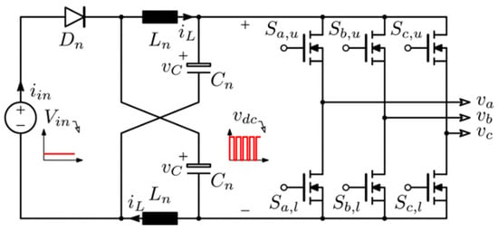
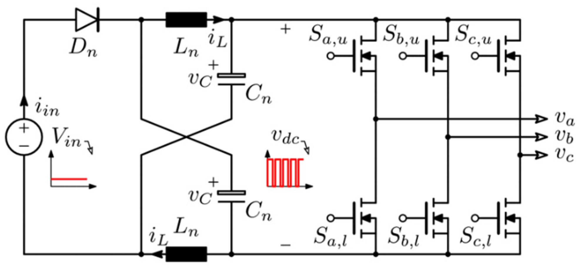
The primary distinction of single-stage converters over two-stage converters is that they have features that minimize the quantity of active and/or passive components within the system. Consequently, the single-stage energy converters incorporate the benefits of both buck and boost converters into a singular device. The most popular single-stage converter is the ZSI, which is known for achieving the voltage boost/buck capabilities and fewer high-frequency components through an extra ST state during the inverter’s switching process [1,6]. Compared to other single-stage converters, the ZSI exhibits lower electromagnetic noise and protects devices from damage when the upper and lower switches of a leg are simultaneously switched ‘on’ [1]. The ZSI shown in Figure 1 consists of the impedance network, which has two inductors and two capacitors connected in an X-shape. The impedance network is fed by either a direct current (DC) voltage source or a current source. The operation involves the charging of the two inductors in the impedance network that results in voltage boosting [7].
Figure 1.
The ZSI network [6].
The operation of the ZSI is in nine switching states, which are classified into two modes: ST and non-ST states [8]. The ST state represents the operation of the inverter due to an additional comparison with the carrier signal. Non-ST state represents the operation of the inverter by comparing the three-phase reference sinusoidal signals with the triangular carrier signal.
3. The Impedance Source Inverter Modulation Strategies
Pulse-width modulation (PWM) is a crucial element in various applications that require DC-to-AC conversion. The uniqueness of PWM control in ZSI is the ability of the ST state, with the aid of the Z-network, to boost the input DC voltage to a desired AC output voltage that is higher than the available DC-link voltage in a single conversion stage. Several PWM techniques can be used to control the generation of the ST duty cycles, which is done by gating on both the upper and the lower switches of the same phase leg. The most common techniques are SBC, MBC, MCBC, and SVM [7]. For all of these modulation schemes, the overall voltage gain G is given by:
where is the peak value of the output phase voltage, is the input DC voltage, M is the modulation index, B is the boosting factor, and is the ST duty cycle, which can be determined by the ST period over the switching cycle T.
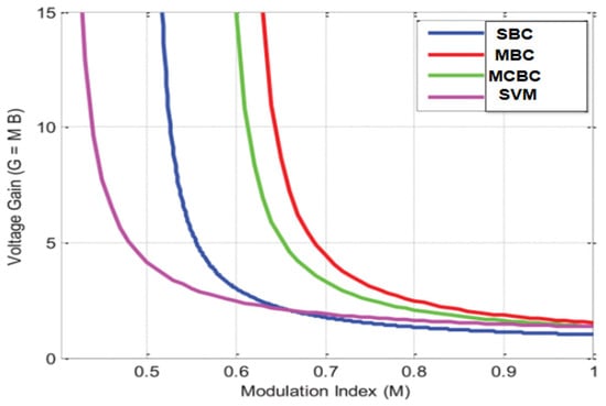
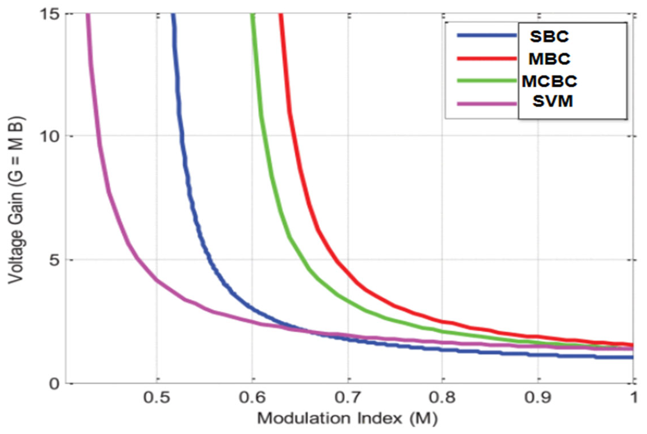
The fundamental characteristic of traditional modulation approaches is the interrelation between the ST duty ratio and the modulation index. As the modulation index decreases, the voltage gain increases, as shown in Figure 2; however, the voltage stress on the capacitor and switching devices intensifies, presenting a challenge in identifying the optimal modulation index that maximizes gain while minimizing voltage stress on passive components and switching devices [6].
Figure 2.
Voltage gain comparison for various ZSI modulation strategies [7].
3.1. Simple Boost Control Method
The SBC method is regarded as the fundamental approach for ZSI topology, as indicated in [9]. It entails comparing three-phase reference signals (Va, Vb, and Vc) with a carrier signal for non-ST operation of the inverter, along with two straight ST lines (Vp and Vn) compared to the carrier for ST operation of the inverter. When the triangular carrier wave is less than or greater than the upper ST reference signal, the ST pulse is generated. Similarly, when the sinusoidal reference signal is greater than the triangular signal, a PWM signal is generated [9]. The ST pulse and the PWM signal are added together, and they are utilized to trigger the inverter switches. The deployment of the SBC system for PV applications yields advantages such as reduced ripple voltage, minimized impedance network size, and increased peak voltage across the inverter switch at the same operating point. Nevertheless, there are disadvantages such as increased voltage stress on switches, reduced voltage gain, and greater switching losses, among others [7].
3.2. Space Vector Modulation Overview
This technique uses the SVM reference signal, with the modulation index serving as an additional reference signal. The triangular carrier signal is used for comparison with the additional reference signal to produce the ST pulse. The SVM signal is analyzed in comparison to the triangular carrier signal to produce the PWM signal, with these signals used to trigger the inverter switches. The SVM demonstrates significant benefits in PV applications, attributed to its ability to provide a smaller component size, the highest gain for any modulation index, and a comparatively broader range of modulation indices. The SVM is a discrete control method that is often operated digitally using high-frequency PWM [7]. According to [7,10], in the traditional modulation strategy, the principle of the SVM scheme starts with the generation of a reference voltage vector (Vref) in the plane as:
where and represent the reference voltage in the plane respectively, and , , and are the three-phase output voltage of the inverter fed to the load/grid.
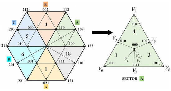
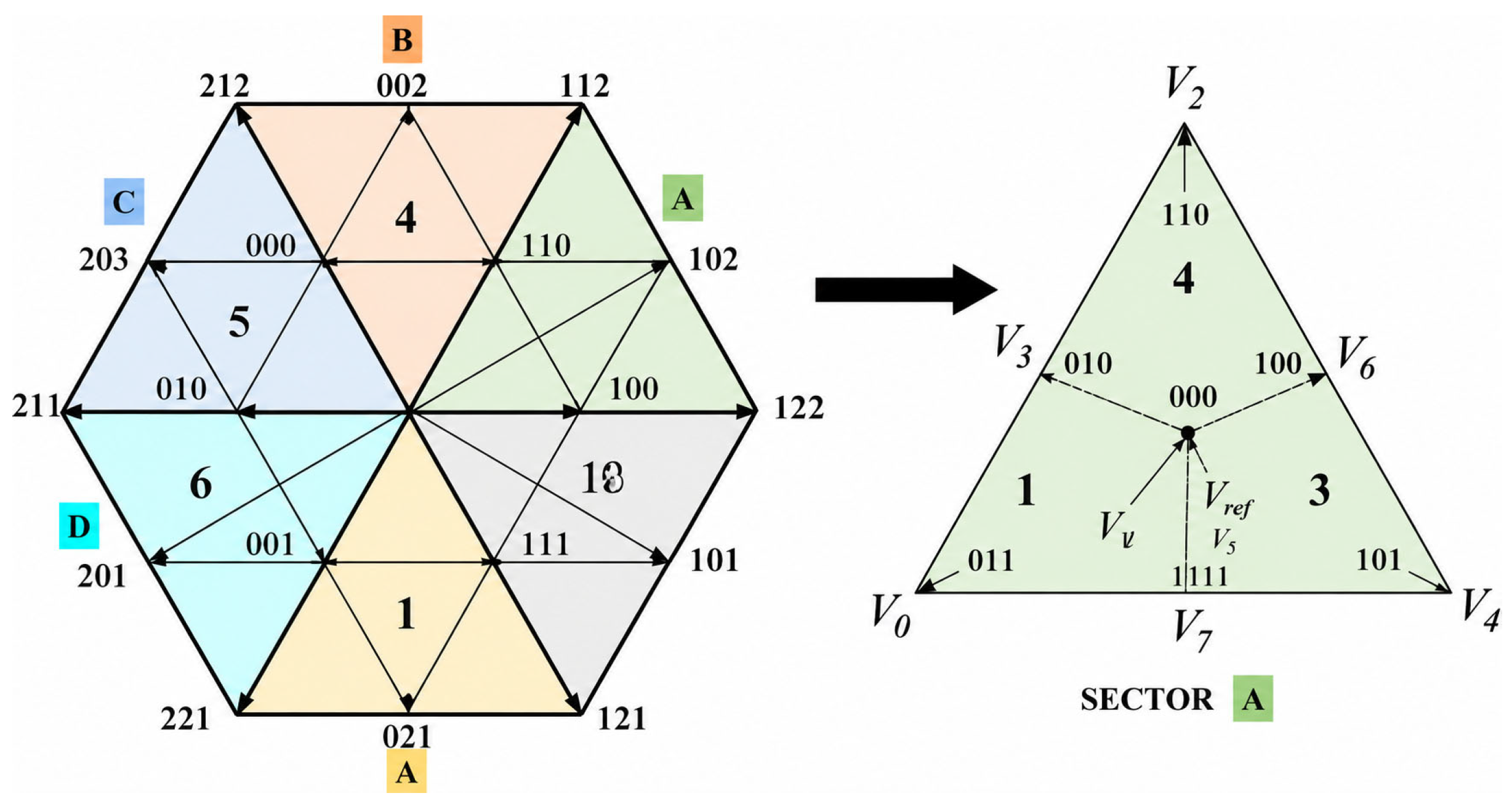
For this technique, there are a total of 27 switching states for the inverter, resulting in 27 space vectors. All the switching sequences can be collectively understood by examining the space vector diagram in Figure 3. The coloured areas reflect the hexagonal space vector plane’s principal sectors, while the number labels designate vector selection triangular sub-sectors. The ternary combinations (000, 110, 221) represent inverter switching setups. Right-side triangular representation reduces reference vector locating and switching times for nearby vectors.
Figure 3.
The SVM space vector diagram [8].
4. The Harmonics Overview
Harmonics can be characterized as a signal or wave whose frequency is an integer multiple of the fundamental frequency. The power delivered frequently exhibits distortion for a variety of reasons, with the total harmonic distortion (THD) index serving as the primary measure of this distortion. THD represents the proportion of distorted power relative to the primary power of the signal [11,12]. Intrinsic harmonic distortions are associated with deficiencies in inverters, including nonlinearities in components and control loops, inaccuracies in measurement, and constraints in PWM resolution.
Linking to a poor and distorted electrical power supply may be viewed as an external influence on the output waveform of the PV system. A distorted voltage in the inverter control system functions as a disturbance, leading to a distortion in the current waveform produced by the inverter [12]. The fluctuations in power density of solar energy resources during PV conversion, influenced by irradiance levels and temperature, lead to variations in voltage and frequency, resulting in sag or swell patterns within the microgrid. To comply with the IEEE 519-2014 standards outlined in Table 1 for various voltage levels, a range of electronic topologies has been employed, including PWM strategies for the inverters [11,13].
Table 1.
Voltage distortion limits according to the IEEE 519 standard [13].
5. The 55-kW PV System Modeling and Design
5.1. Environmental Input Parameters
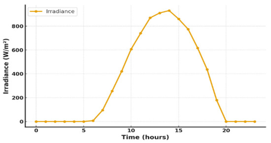
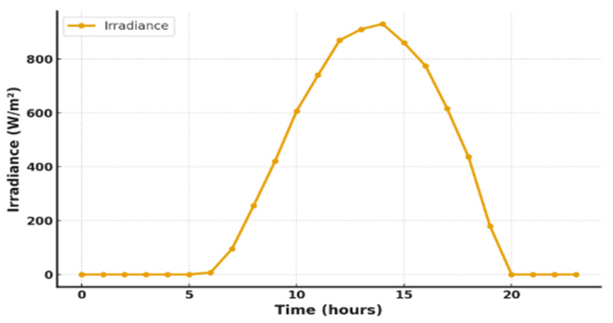
The 55 kW standalone PV system integrated with a PEMFC was modeled in MATLAB/Simulink R2024b. The parameters of the PV array were derived from standard manufacturer data, while environmental inputs, including irradiance and temperature, were varied for both standard test conditions (STC) and dynamic variations characteristic of high-irradiance regions sourced from PVGIS, such as the Northern Cape, as illustrated in Figure 4 [2].
Figure 4.
Northern Cape daily irradiance profile.
5.2. PV Array Design, ZSI, and LCL Filter Design Parameters
The specifications of the PV panel are summarised in Table 2. The array voltage is 342.9 V, while the DC link voltage is set at 514.35 V [2].
Table 2.
CS6U-345M Polycrystalline PV solar panel parameters.
The ZSI and LCL parameters are presented in Table 3.
Table 3.
The ZSI and LCL filter parameters.
6. The System Results
6.1. System with the SBC Scheme Under STC
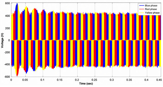
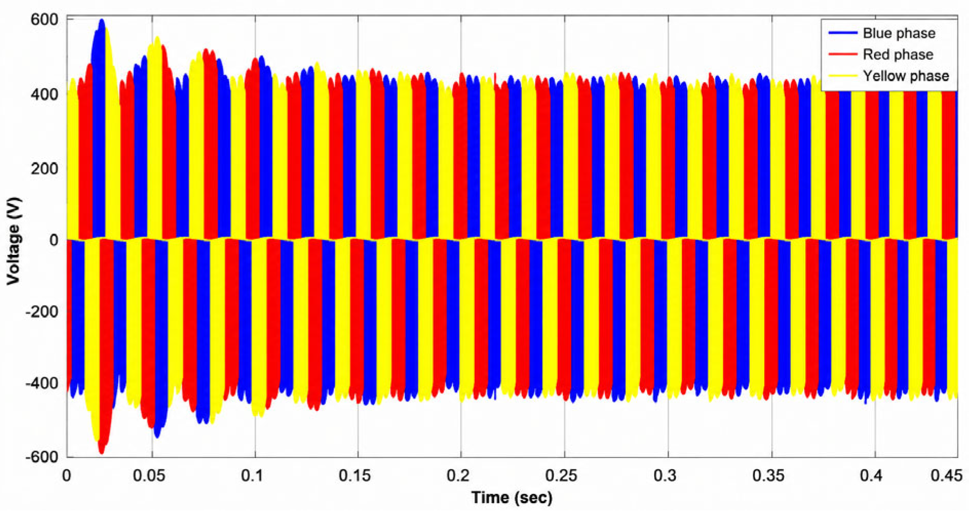
The voltage performance of the PV-FC system using the SBC technique was examined under STC to evaluate its dynamic behavior and power quality. In Figure 5, the system was evaluated without the PEMFC, and the output voltage exhibited significant oscillations, harmonic distortion, and reduced voltage regulation accuracy. The SBC successfully provided the required boost capability, but its control simplicity limited its ability to regulate voltage stability.
Figure 5.
The system using the SBC voltage waveforms without the PEMFC.
With the PEMFC integrated into the DC bus, a marked improvement in voltage stability and waveform symmetry was observed, as shown in Figure 6. This stabilization effect translated into smoother inverter waveforms, balanced phase amplitudes, and substantially reduced THD levels. The PV-PEMFC integration mitigated transient voltage deviations and suppressed switching-related noise inherent in the SBC technique.
Figure 6.
The system using the SBC voltage waveforms with the PEMFC.
6.2. System with the SVM Scheme Under STC
In the PV-only configuration, the inverter output voltage exhibited a relatively smooth sinusoidal waveform compared to the SBC case, as shown in Figure 7. The optimized switching sequence inherent in SVM reduced harmonic distortion, resulting in an improved voltage waveform and higher fundamental voltage utilization.
Figure 7.
The system using the SVM voltage waveforms without the PEMFC.
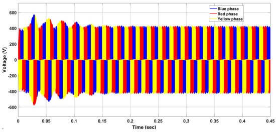
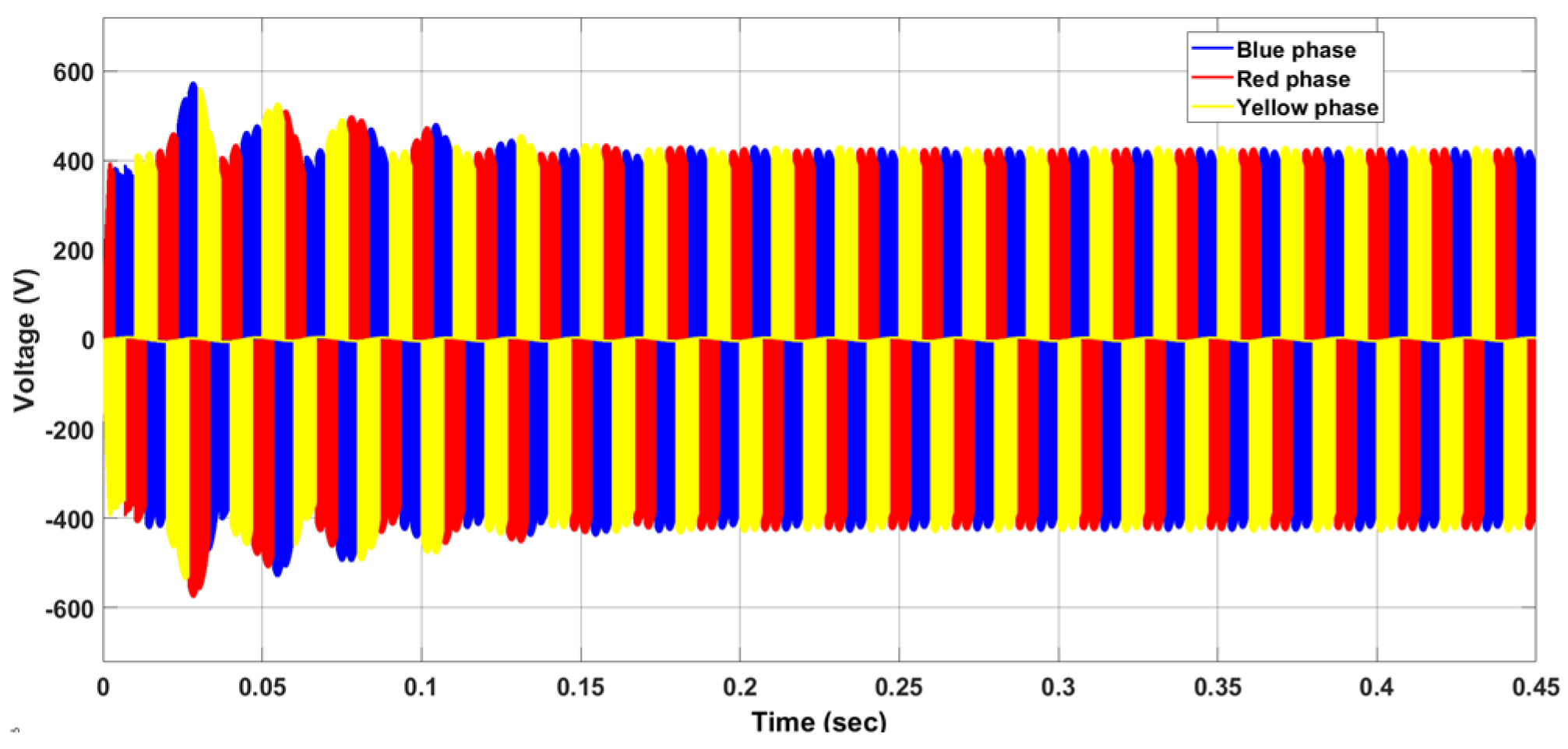
The inclusion of the PEMFC provides an auxiliary and DC power source that effectively regulates the DC-link voltage of the inverter, with the system attaining steady-state conditions within approximately 0.03 s, as illustrated in Figure 8. This integration enhances the dynamic response of the system. It ensures that the SVM technique in the inverter synthesizes balanced voltages with reduced ripple and THD.
Figure 8.
The system using the SVM voltage waveforms with the PEMFC.
6.3. System with the SBC Scheme Under Varying Conditions
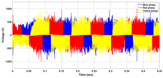
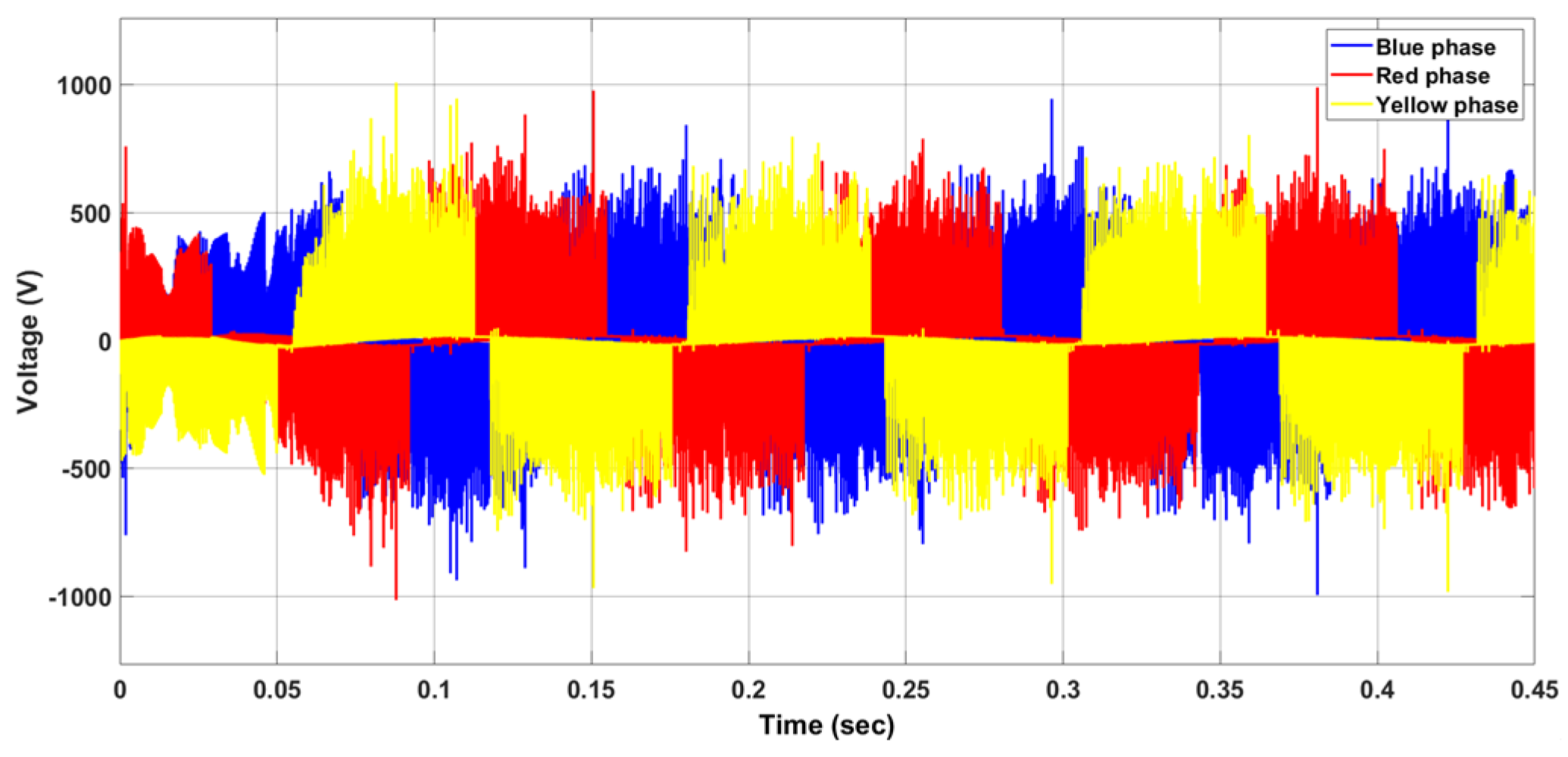
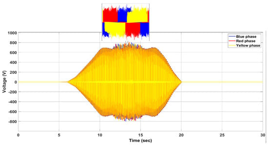
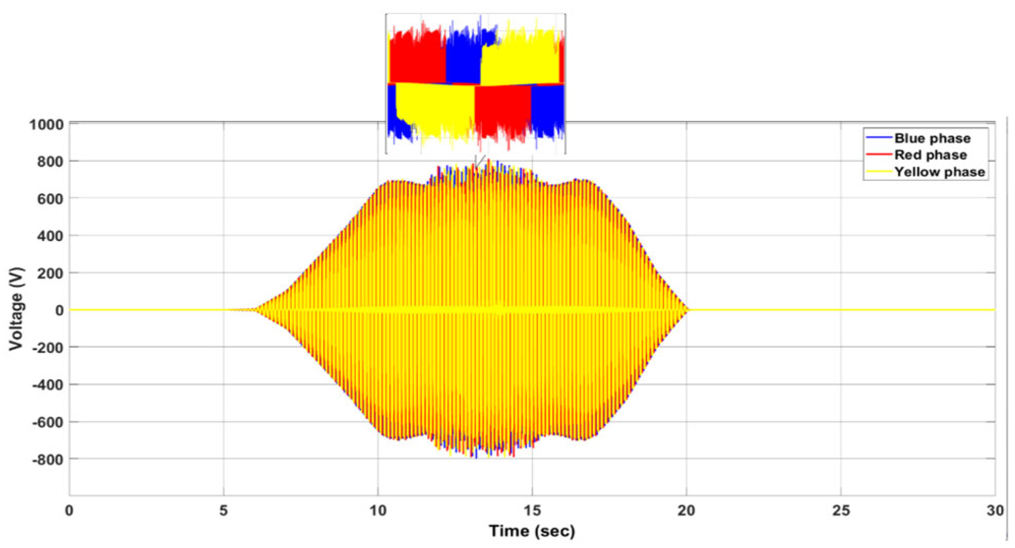
Figure 9 illustrates the three-phase voltage profiles of the PV system operating under dynamic irradiance conditions using an SBC technique without the PEMFC, with the system nearly reaching 800 V during peak times. However, due to the inherent delay and limited dynamic response of the SBC, the ZSI experiences transient overshoot and undershoot in the DC-link voltage. Although the SBC performs acceptably under dynamic irradiance, its control bandwidth is insufficient to fully mitigate the transient effects of rapid solar changes.
Figure 9.
The PV system voltage profile under varying conditions.
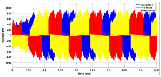
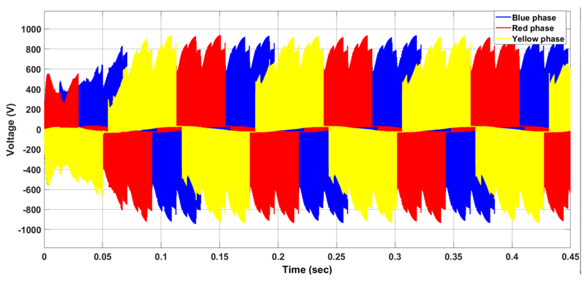
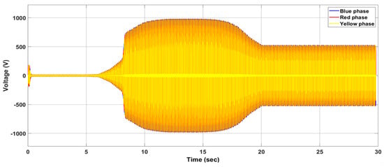
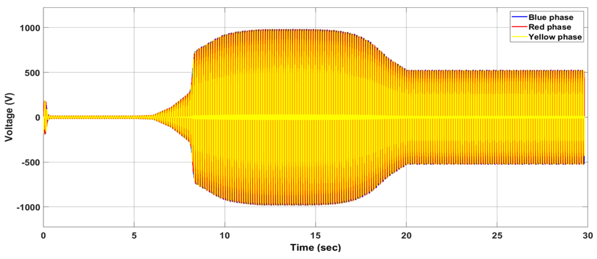
With the PEMFC integration, the system exhibits an improvement in both voltage magnitude and waveform quality as the system reaches approximately 1000 V at the irradiance peak, as depicted in Figure 10. The transient distortions during the irradiance variation are reduced, as the PEMFC acts as a complementary power source; the SBC benefits from a more stable and buffered input power profile. The variation in the duty cycle of the SBC becomes less noticeable as the PEMFC successfully addresses the fluctuations in PV power that could otherwise hinder the performance of the controller’s regulation.
Figure 10.
PV-PEMFC voltage profile under dynamic conditions.
6.4. System with the SVM Scheme Under Varying Conditions
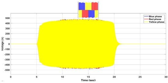
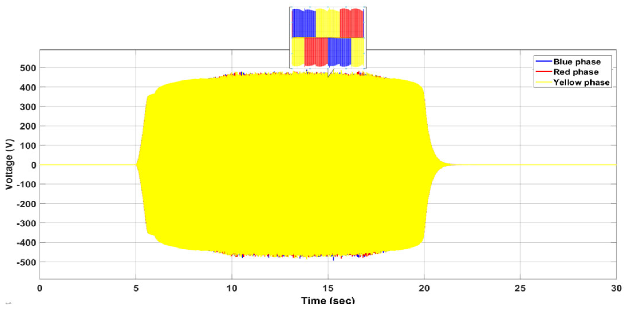
Figure 11 represents the voltage waveforms of the PV system operating under dynamic irradiance using the SVM technique without the integration of the PEMFC. At low irradiance, the PV array generates insufficient power to maintain the DC-link voltage, resulting in a 0 V voltage output. As the irradiance increases, the system’s voltage reaches a peak voltage of approximately 500 V. While the SVM ensures accurate phase displacement and effective harmonic suppression, its performance is limited by the variable and constrained DC-link voltage provided by the PV array. The SVM works to maintain voltage vector balance by consistently modifying the active and zero switching vectors to ensure a sinusoidal reference trajectory is upheld.
Figure 11.
The PV system voltage profile under varying conditions.
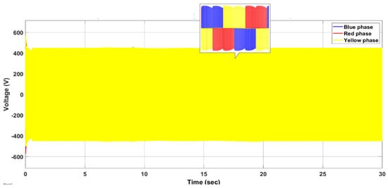
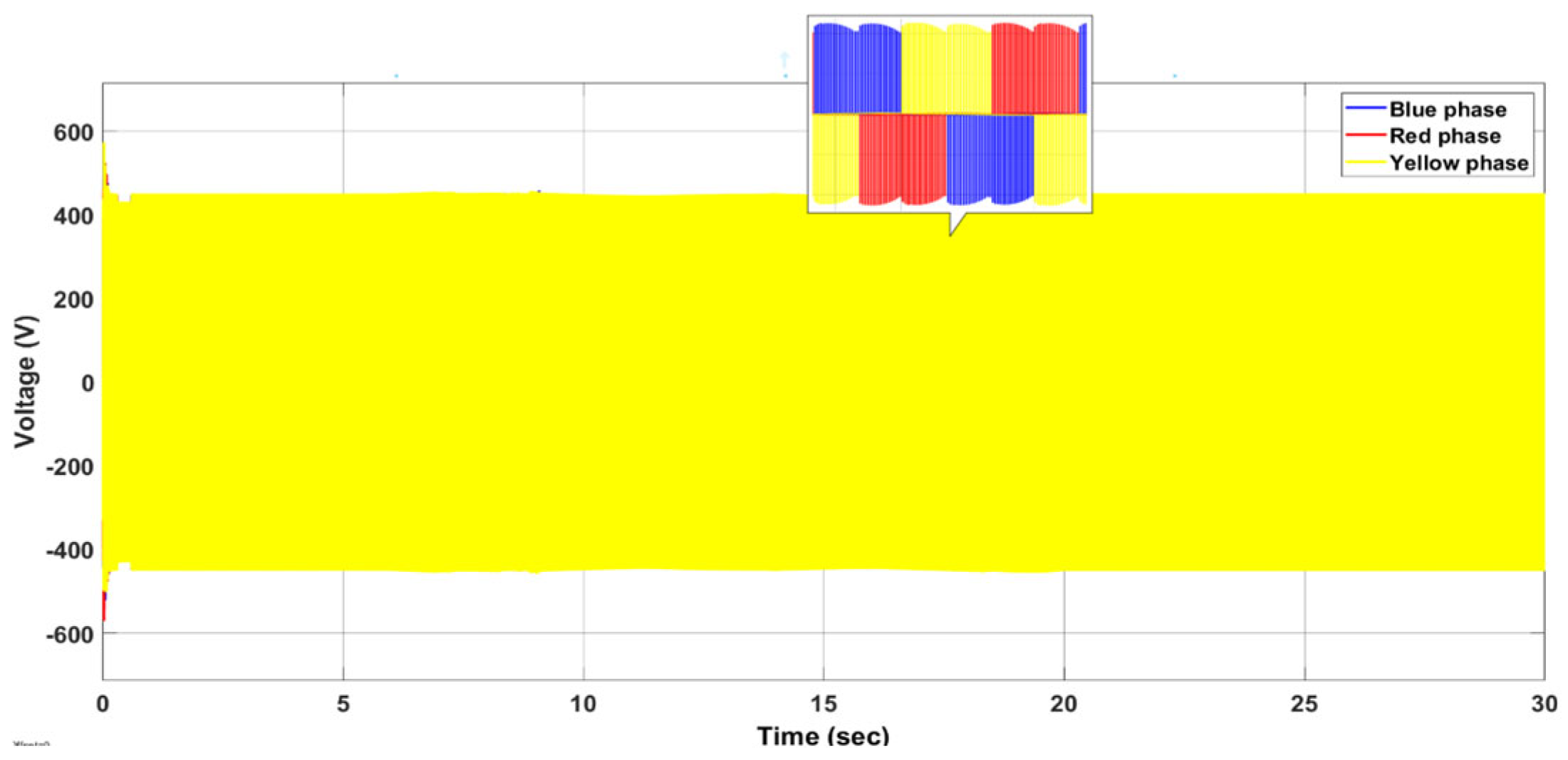
The PEMFC integration to the system provides an auxiliary power path that stabilizes the DC-link voltage and supports the ZSI during irradiance variation, as shown in Figure 12. The SVM demonstrates a more proactive and effective function in this configuration. The stabilized DC-link offered by the PEMFC allows the SVM algorithm to function at its optimal modulation index, facilitating precise voltage vector synthesis. The outcome is a notable enhancement in voltage linearity, a decrease in THD, and an improvement in the dynamic tracking of reference vectors. The SVM persistently modifies the switching patterns to uphold balanced phase voltages, guaranteeing accurate vector trajectory and consistent phase amplitude across different load and irradiance scenarios.
Figure 12.
The voltage profile of the PV system integrated with the PEMFC under dynamic conditions.
7. Conclusions
This study presented a comparative evaluation of two key modulation strategies, SBC and SVM, implemented within a PV-PEMFC microgrid system. The evaluation was performed under both STC and dynamic irradiance conditions to assess voltage regulation, THD, and transient performance. The simulation results indicated that, although the SBC offers structural simplicity and efficient voltage enhancement, its constrained dynamic response leads to transient oscillations and increased voltage ripple amid changes in irradiance. The integration of the PEMFC effectively addressed these challenges by stabilizing the DC-link voltage, minimizing harmonic distortion, and enhancing phase balance. The SVM technique demonstrated enhanced performance within the system, effectively maintaining balanced three-phase voltages while minimizing distortion and achieving quicker transient recovery.
The integration of the PEMFC allowed the SVM to attain optimal modulation index utilization, resulting in increased output voltage amplitude, reduced THD, and improved dynamic stability. The integration of PEMFC significantly improved the operational reliability of both control schemes, with SVM demonstrating the highest effectiveness in enhancing inverter performance and ensuring power quality across different solar conditions. Future work will focus on integrating the filter system to further minimize THD and enhance overall dynamic power quality.
Author Contributions
Conceptualization, methodology, software, M.S.M.; validation, M.S.M., E.O. and N.C.; formal analysis, investigation, writing—original draft preparation, M.S.M.; writing—review and editing, E.O.; visualization, M.S.M.; supervision, E.O. and N.C. All authors have read and agreed to the published version of the manuscript.
Funding
This research received no external funding.
Institutional Review Board Statement
Not applicable.
Informed Consent Statement
Not applicable.
Data Availability Statement
This research includes the original contributions offered in the article. Additional enquiries may be sent to the corresponding author.
Conflicts of Interest
The authors declare no conflicts of interest.
References
- Abdelhakim, A.; Davari, P.; Blaabjerg, F.; Mattavelli, P. An improved modulation strategy for the three-phase Z-source inverters (ZSIs). In 2017 IEEE Energy Conversion Congress and Exposition (ECCE); IEEE: Piscataway, NJ, USA, 2017; pp. 4237–4243. [Google Scholar]
- Maduna, M.S.; Chetty, N.D.; Ojo, E.E. Design and Simulation of a Solar Photovoltaic System Embedded with a Hydrogen Fuel Cell Storage System. In 2025 Conference on Information Communications Technology and Society (ICTAS); IEEE: Piscataway, NJ, USA, 2025; pp. 1–6. [Google Scholar]
- Gautam, S.P.; Jalhotra, M.; Sahu, L.K.; Kumar, M.R.; Gupta, K.K. A survey on fault tolerant and diagnostic techniques of multilevel inverter. IEEE Access 2023, 11, 60866–60888. [Google Scholar] [CrossRef] [Scilit]
- Liu, P.; Xu, J.; Yang, Y.; Wang, H.; Blaabjerg, F. Impact of modulation strategies on the reliability and harmonics of impedance-source inverters. IEEE J. Emerg. Sel. Top. Power Electron. 2019, 8, 3968–3981. [Google Scholar] [CrossRef] [Scilit]
- Nandhini, E.; Sivaprakasam, A. A review of various control strategies based on space vector pulse width modulation for the voltage source inverter. IETE J. Res. 2022, 68, 3187–3201. [Google Scholar] [CrossRef] [Scilit]
- Noui, S.; Tabbache, B.; Berkouk, E.-M.; Benbouzid, M. A Pulse-Width Modulation Control Approach for the High-Voltage Gain Operation of a Z-Source Neutral-Point Clamped Inverters. IETE J. Res. 2023, 69, 7374–7393. [Google Scholar] [CrossRef] [Scilit]
- Gyawali, B.; Ajmal, A.M.; Liu, W.; Yang, Y. A review on modulation techniques of Quasi-Z-source inverter for grid-connected photovoltaic systems. E-Prime-Adv. Electr. Eng. Electron. Energy 2024, 10, 100809. [Google Scholar] [CrossRef] [Scilit]
- Hasan Babayi Nozadian, M.; Babaei, E.; Hosseini, S.H.; Shokati Asl, E. Switched Z-source networks: A review. IET Power Electron. 2019, 12, 1616–1633. [Google Scholar] [CrossRef] [Scilit]
- Roomi, M.M. An Overview of Carrier-based Modulation Methods for Z-Source Inverter. Power Electron. Drives 2019, 4, 15–31. [Google Scholar] [CrossRef] [Scilit]
- Agrawal, K.; Gandhi, A.; Shah, M.; Gojiya, M. Design, analysis and realization of SVPWM using embedded code generation technique for a three phase, two level inverter. In 2016 International Conference on Electrical Power and Energy Systems (ICEPES); IEEE: Piscataway, NJ, USA, 2016; pp. 377–382. [Google Scholar]
- Pereira, J.L.M.; Leal, A.F.R.; Almeida, G.O.d.; Tostes, M.E.d.L. Harmonic effects due to the high penetration of photovoltaic generation into a distribution system. Energies 2021, 14, 4021. [Google Scholar] [CrossRef] [Scilit]
- Yuan, W.; Yuan, X.; Xu, L.; Zhang, C.; Ma, X. Harmonic loss analysis of low-voltage distribution network integrated with distributed photovoltaic. Sustainability 2023, 15, 4334. [Google Scholar] [CrossRef] [Scilit]
- Langella, R.; Testa, A.; Alii, E. IEEE recommended practice and requirements for harmonic control in electric power systems. In IEEE Recommended Practice; IEEE: Piscataway, NJ, USA, 2014. [Google Scholar]

Disclaimer/Publisher’s Note: The statements, opinions and data contained in all publications are solely those of the individual author(s) and contributor(s) and not of MDPI and/or the editor(s). MDPI and/or the editor(s) disclaim responsibility for any injury to people or property resulting from any ideas, methods, instructions or products referred to in the content. |
© 2026 by the authors. Licensee MDPI, Basel, Switzerland. This article is an open access article distributed under the terms and conditions of the Creative Commons Attribution (CC BY) license.