


Abstract
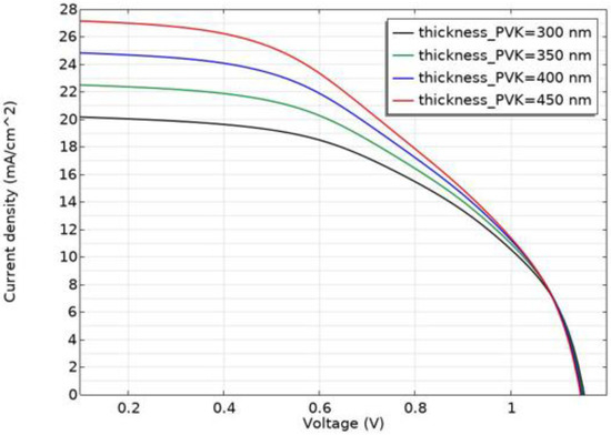
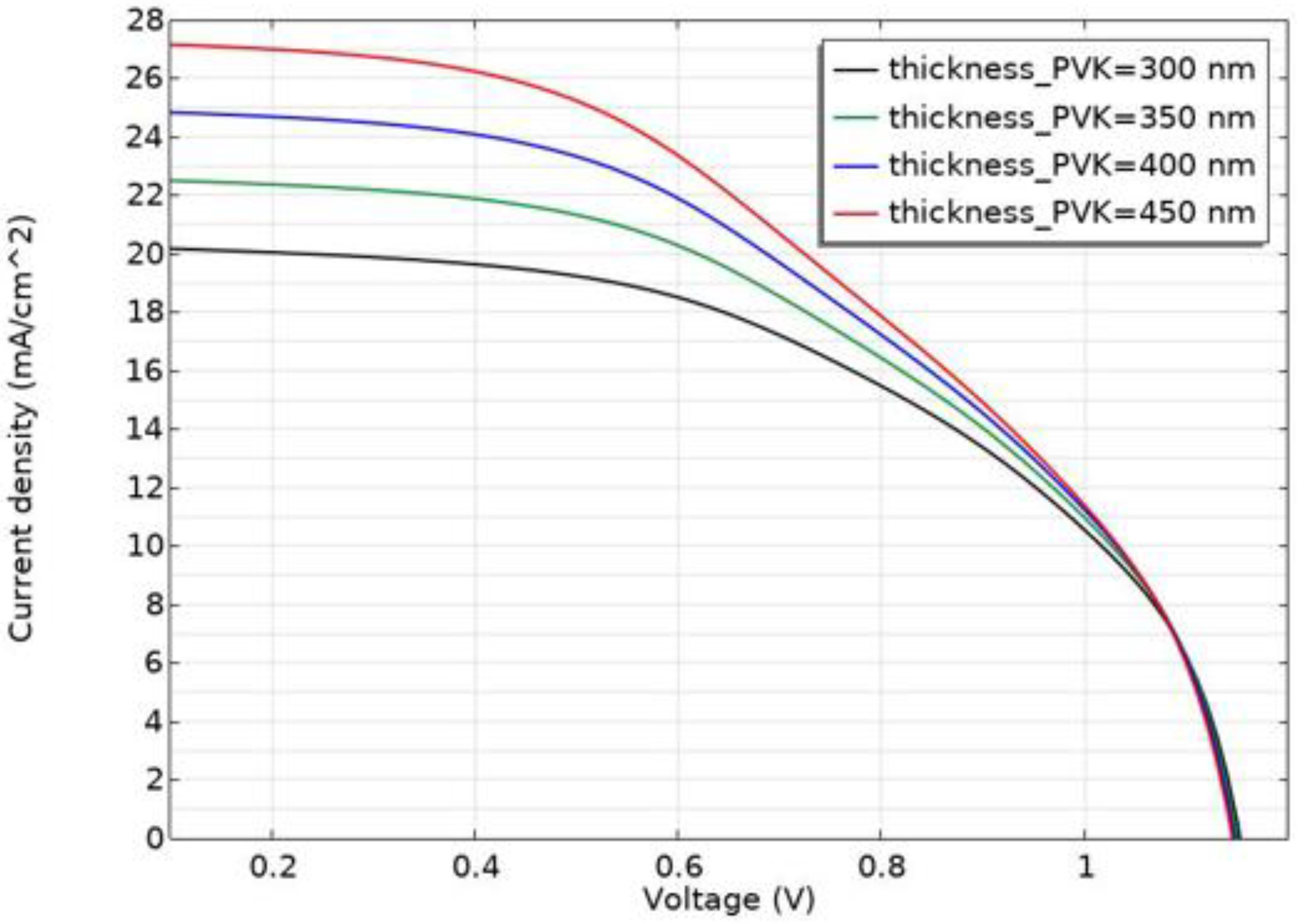
Perovskite solar cells in aerospace applications are promising due to their high power output, radiation tolerance, and ability to extend spacecraft operational lifetimes. Numerical modelling is widely used to optimize solar cells as it can predict the real-world behavior of a device. In this work, we present a numerical simulation of CsMAFA-based perovskite solar cells with monolayer graphene as the front electrode. The model is implemented in the COMSOL Multiphysics® finite-element environment. Graphene is modelled using the Kubo formula to account for its frequency-dependent surface conductivity, and the electromagnetic wavs interface is coupled with the semiconductor module to capture optical–electrical interactions. The influence of absorber layer thickness on the current density is also examined by sweeping the perovskite absorber thickness (300–450 nm). The current voltage characteristic demonstrates higher current density (27 mA/cm2) at an absorber thickness of ~450 nm. Shockley–Read–Hall recombination (SRH) is studied inside the model and maximum recombination was found to be centred in the absorber layer. The graphene/HTL side shows an SRH recombination of 2 × 1020 cm−3 s−1, which is much lower than what is typically seen at ITO-based HTL interfaces.
1. Introduction
Environmental concerns all over the world and increasing energy demands are fueling the need for the utilization of alternative natural energy resources. The emission of greenhouse gases from burning fossil fuels like coal and gas is the main obstacle to a healthy atmosphere. The emitted gases contribute greatly to climate change all over the globe [1]. The European Union adapted the strategy of 600 GW solar installation to address these concerns and meet the needs of the European Green Deal by the end of 2030 [2]. Solar energy is currently considered the most abundant yet affordable of all natural resources [3]. Employing natural light obtained from the sun to produce electrical energy is one of the most promising solutions to the world’s energy crisis [4]. Natural light from the sun is composed of electromagnetic radiation. According to quantum mechanics theory, all radiation consists of photons, uncharged and massless particles [5]. Solar cells are photovoltaic (PV) cells based on semiconductor material that have the capacity to absorb photons from natural light directly and transform them into electrical energy through the photovoltaic effect. When light hits the solar cell surface, it excites the electrons to a higher energy state. In semiconductor materials, these electrons become free charge carriers, thus creating electron–hole pairs [6]. Electrons flow through the n-region, while holes move through the p-region, creating an electric current that can be processed by diodes and used in an external circuit [7]. Powering aircraft with solar energy may be a promising solution for green transportation. The abundance of solar energy on Earth ensures the affordability of this technology. Solar aircraft can reduce environmental impacts, fuel consumption, and operational cost and extend the flight duration. The concept of solar-powered aircraft requires a photovoltaic device to provide efficient energy conversion. A rechargeable battery can be used to store the energy produced in the daytime that could benefit the system at night [8]. Significant advancements in solar-powered aircraft technology are observed in the literature analysis below. In 1974, the first solar aircraft with monocrystalline solar cells, Sunrise I, was installed, and demonstrated 450 W power and 11% efficiency [9]. In 1980, Dr. Paul MacCready created a human-crewed aircraft named Gossamer Penguin with monocrystalline cells. A solar challenger mounted on the aircraft wings produced 2500 W of power [10]. The progression of technology over time can be highlighted by the fact that in 2005, SoLong, powered by a monocrystalline solar cell, was developed by Alan Cocconi by incorporating a lithium-ion battery as a storage device, providing 225 W of power [11]. In 2009, Solar Impulse I utilized monocrystalline solar cells, resulting in 18% efficiency and 84 W power [12]. Moving towards aircraft using amorphous silicon, in 2010, Zephyr 7, with a lithium sulphur battery, demonstrated an efficiency of 19% [13]. Solar Impulse II contained a total of 17,248 monocrystalline solar cells and a lithium-ion battery that produced 66 KW power, embarking on a global journey from 2014 to 2016 [14].
Solar-powered aircraft design requires three main components: a maximum power point tracker, photovoltaic cell, and rechargeable battery [15]. Our focus in this study is the second component, the photovoltaic cell. Perovskite solar cells are becoming more important for aerospace applications because they are lightweight, flexible, and have great radiation tolerance. Mixed-cation CsMAFA perovskite has recently gained attention when used to replace the conventionally used CH3NH3PbI3 (MAPbI3). CsMAFA offers better stability when exposed to UV light, vacuum, and temperature, which are the main stressors in space. Adding Cs helps the lattice remain stable, FA makes it more resistant to heat, and MA helps with good crystallization and film formation, which overall makes the absorber more durable. In general, CsMAFA perovskites are better at preserving their structure and optoelectronic properties than MAPbI3, which makes them preferable for space solar cells [16].
In parallel, graphene-based materials are being increasingly explored in space solar cell architectures due to their multifunctional properties, such as high thermal conductivity, mechanical robustness, and resistance to radiation damage. These characteristics make graphene an attractive candidate for enhancing charge transport, thermal management, and overall device durability under the extreme thermal, mechanical, and radiation stresses encountered in space [17]. An important step during the design process of a solar cell is to predict the performance of a component in short time periods. Using simulation means that less effort is required for the design and leads to a more reliable design with less failures. Developing a reliable model can save costs and time in experiments, leading to a robust design by overcoming the conventional trial-and-error methods [18]. While several numerical studies based on COMSOL and SCAPS have investigated conventional MAPbI3 perovskite solar cells, we have incorporated triple-cation CsMAFA perovskite solar cells. Moreover, transparent electrodes are usually modelled using simplified bulk conductivity or ideal contact assumptions. In this work, graphene is explicitly modelled as an ultrathin two-dimensional electrode using the Kubo formula, allowing its frequency-dependent surface conductivity to be coupled directly with optical and semiconductor physics. Moreover, Shockley–Read–Hall recombination is not treated as a fitting parameter but is spatially resolved across the full device stack to identify dominant recombination regions.
In this paper, we address the optimization of photovoltaic cell design by employing graphene electrodes. The effect of thickness of perovskite absorber on the J-V characteristics is analyzed by means of numerical simulations. Shockley–Read–Hall recombination is also studied across the structure of the solar cell at maximum power point voltage (Vmpp). The effect of graphene in reducing SRH recombination at the HTL/perovskite interface is evaluated.
2. Numerical Modelling Approach
Numerical modelling is the process of designing computerized models that are based on a real-life system. This is beneficial for predicting behavior and building an operational strategy before investing significant money on experimentation [19]. Simulation provides insight into the behavior of real systems [20]. The finite-element commercial software COMSOL Multiphysics® v 6.2 (COMSOL Inc., Burlington, MA, USA) is used in this work as it is a powerful tool for solving partial differential equations and the multiphysics modelling of solar cells, providing the possibility of multiphysics simulations that can couple semiconductor physics with optical and electrical modules [21].
The semiconductor module is used for determining the electric potential and the electron and hole concentration within the desired geometry. The module solves the Poisson and carrier drift–diffusion equations, enabling calculation of short-circuit current density (Jsc), open-circuit voltage (Voc) and efficiency [22]. The semiconductor module is coupled with the electromagnetic waves, frequency domain (ewfd) interface to study the optical generation inside the solar cell. The ewfd interface is also used to model graphene as a surface current density by using the Kubo formula. This boundary feature of ewfd allows the extremely thin conductive layers to be modelled without the necessity to be meshed as a bulk domain [23].
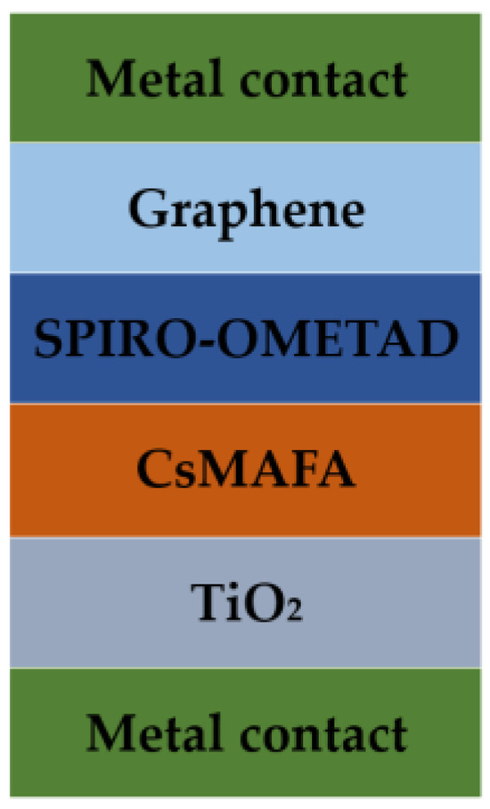
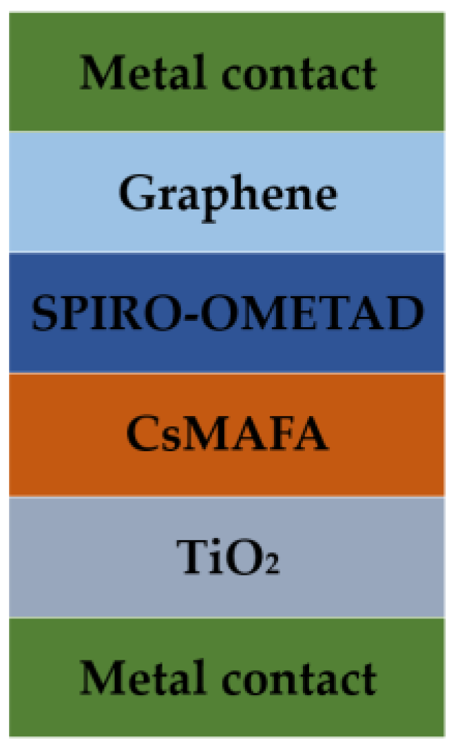
The numerical simulations were performed under steady-state conditions using a coupled optical–electrical semiconductor model. Uniform photogeneration was assumed within the active layers, with equal electron and hole generation rates. Trap-assisted recombination was modelled using the Shockley–Read–Hall (SRH) formula, with electron and hole lifetimes taken from material parameters. Ideal ohmic metal contacts were applied at both electrodes, with the bottom contact fixed at 0 V and an external bias applied at the top contact. Scattering boundary conditions were applied to suppress artificial reflections. All simulations were carried out at room temperature. Optical transitions were modelled using a direct band-gap approach, accounting for stimulated and spontaneous emission to ensure optoelectronic coupling. The device architecture of the considered solar cells includes graphene electrodes as the top part of the regular structure. A thin monolayer of graphene (0.32 nm) is employed on the top of the hole transport layer (HTL) in the modelled structure. The schematic of the solar cell structure considered in this study can be seen in Figure 1.
Figure 1.
Schematic diagram of proposed geometry (thickness of the layers not to scale).
3. Finite-Element Method
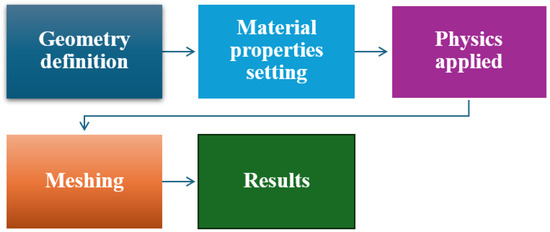
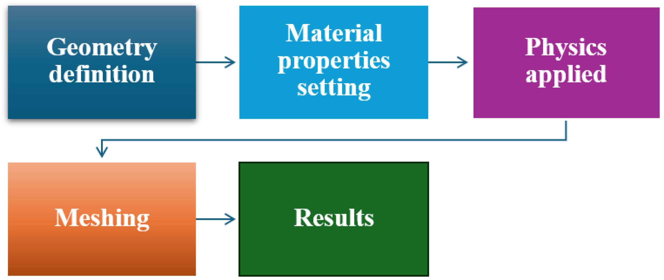
The finite-element method (FEM) is a numerical experiment that can save the cost of real-life experiments [24]. The computational method is based on dividing a complex problem into simpler parts [25]. Linearized partial differential equations are therefore solved with this method over entire complex geometries, after applying suitable boundary conditions based on the real-life situation represented. The “divide and conquer” principle best describes the core meaning of this numerical method. The complex systems can be divided into smaller sub-systems, i.e., the finite elements, during the meshing operation. These elements are connected to each other and each connection point is referred to as a node. A simple approximation of the field is considered in each element. Complex partial differential equations are converted to simple sets of linear equations, describing the behavior of a field in that specific element. The total behavior of the system is analyzed by considering the individual elements and their interaction [26]. The 5 steps methodology of FEM used in this work is depicted in Figure 2 below.
Figure 2.
Finite-element method steps.
3.1. Geometry
The p-i-n solar cell device is composed of SPIRO-OMETAD C81H68N4O8 as the hole transport layer (HTL) [27], a CsMAFA absorber as the active layer, and titanium dioxide (TiO2) as the electron transport layer (ETL) [28]. On the top of the HTL, there is a thin monolayer of graphene that corresponds to the non-ideal electric contact, as shown in Figure 1. The metal contact overlaps with the graphene layer on the top, with the voltage set to 0 V. A second metal contact is at the bottom of the structure and a voltage sweep is carried out from 0 to 1.2 V [29]. The described schematic was built in the geometry section of COMSOL by using the parameters defined in Table 1. These parameters were set in the global definition of the COMSOL interface. Semiconductor physics coupled with the electromagnetic waves, frequency domain (ewfd) interface is applied to the geometry.
Table 1.
Device simulation parameters.
3.2. Material Properties
All the required material properties were input into the COMSOL Multiphysics software for the calculation. Graphene is modelled via the Kubo formula by applying the surface current density boundary condition. This boundary condition is , whereas Ω is the total conductivity of the inter- and intra bands of graphene described by the Kubo formula [30].
4. Discussion and Results
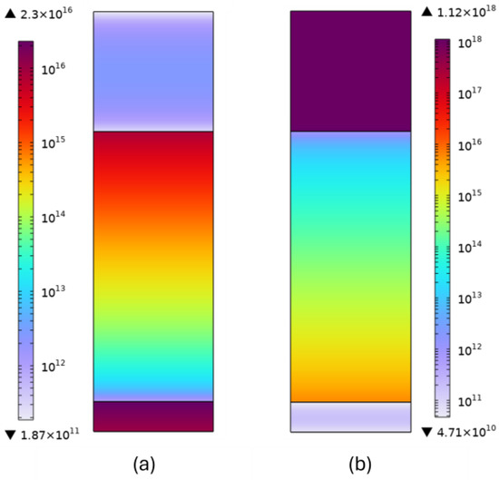
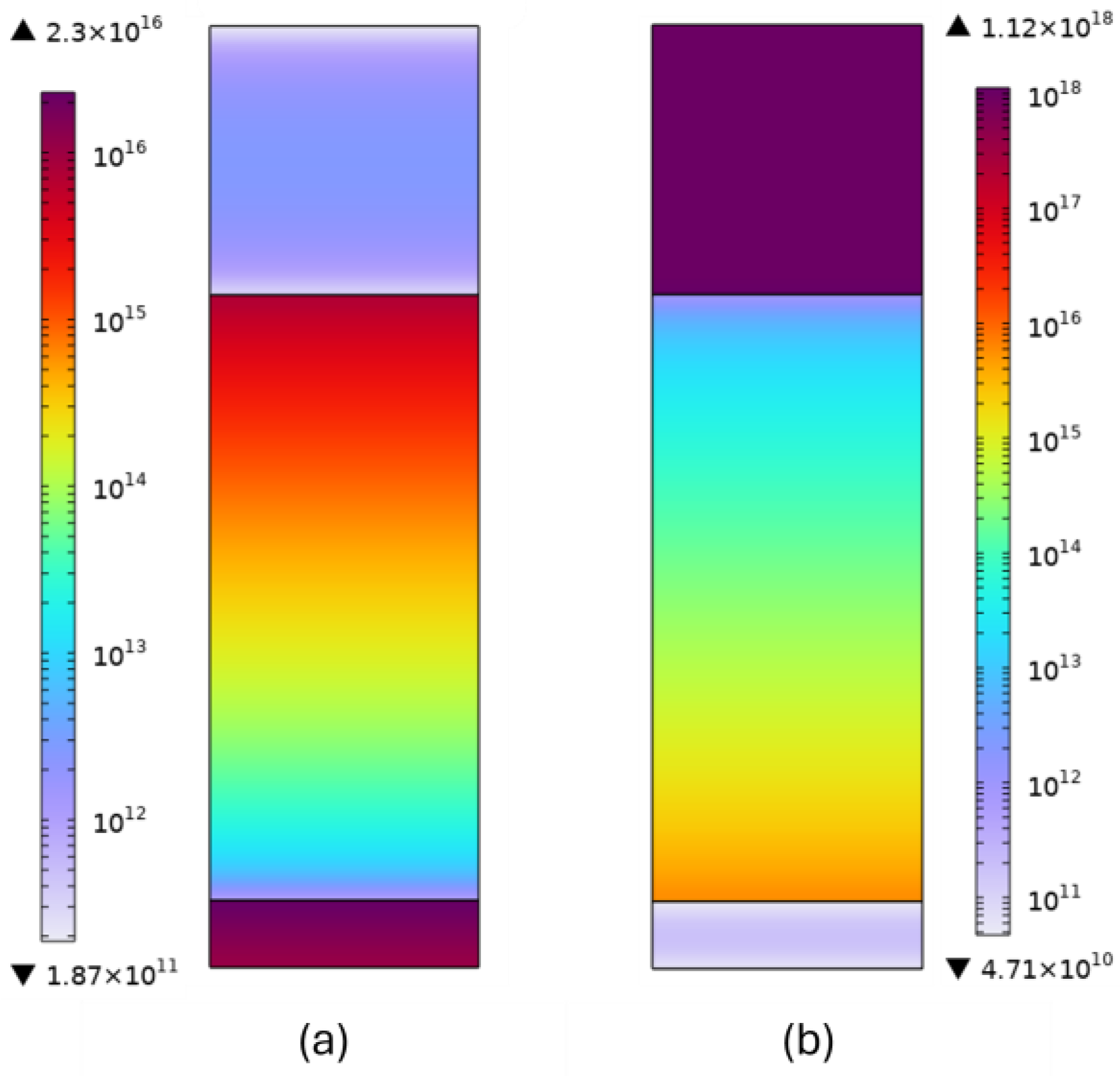
The main results of the stationary solution computation are the electron and hole concentrations, shown in Figure 3a,b, respectively. The electron concentration is shown in Figure 3a at 0.65 V. At the bottom interface (perovskite/TiO2), the electron density reaches 2 × 1016 cm−3, reflecting efficient electron extraction and majority carrier accumulation near the ETL. Near the top Spiro-OMeTAD/graphene contact, the electron density drops to its minimum (~1012 cm−3) as the hole-selective interface blocks electrons and maintains a low minority-carrier population. In Figure 3b, the hole concentration is at the maximum at the SPIRO-OMETAD 1.1 × 1018 cm−3 and lowest in the ETL, suggesting favorable extraction of holes at the HTL/perovskite interface. This distribution represents the expected behavior of a p-i-nperovskite stack, where electrons are confined toward the ETL and suppressed toward the HTL and vice versa [31].
Figure 3.
Carrier concentrations: (a) electron concentration, (b) hole concentration.
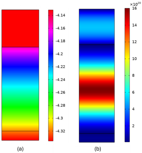
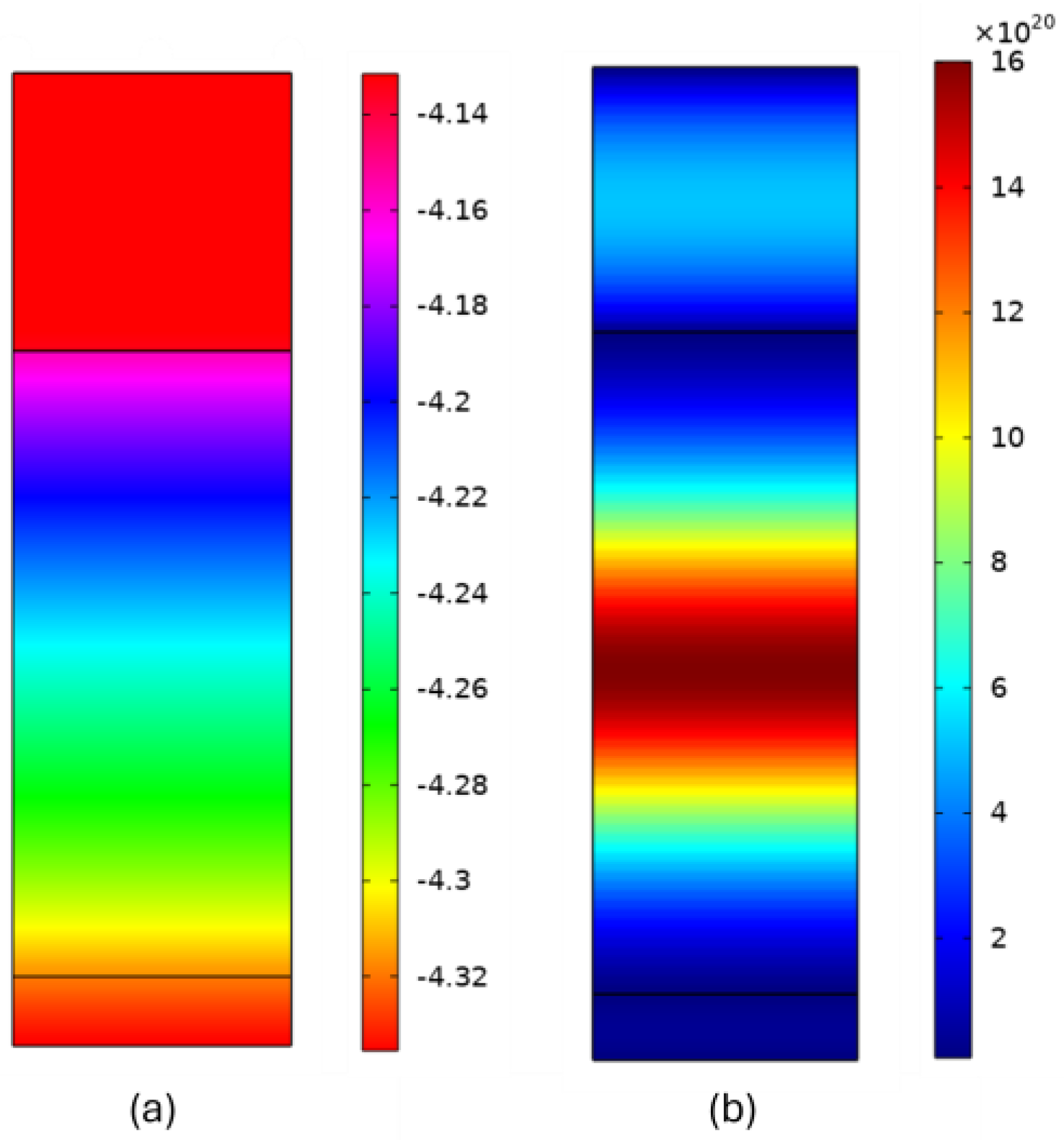
At 0.65 V, the electric potential profile across the device shows a smooth and monotonic drop (Figure 4a), characteristic of a well-behaved p-i-n perovskite junction. The potential is highest near the Spiro-OMeTAD/graphene interface (approximately −4.15 V, red region) and decreases steadily through the CsMAFA absorber, falling to roughly −4.32 V at the TiO2 side. A strong gradient occurs within the perovskite bulk, reflecting the combined effect of the built-in electric field and the externally applied forward bias. In contrast, both transport layers show relatively flat potential regions consistent with their high conductivity and selective contact behavior. This potential distribution confirms efficient band bending at the ETL and HTL interfaces and supports the observed carrier transport pattern with electrons driven toward TiO2 and holes toward Spiro-OMeTAD [32]. Shockley–Read–Hall recombination (Figure 4b) under 0.65 V bias shows that trap-assisted recombination is highest in the CsMAFA perovskite layer and diminishes toward both contacts, with notably lower SRH activity at the graphene/Spiro-OMeTAD (HTL) and perovskite/TiO2 (ETL) interfaces. This profile indicates that bulk defects dominate the nonradiative recombination in the device, while well-passivated interfaces contribute minimal SRH losses. The recombination pattern is consistent with literature modelling of similar planar p-i-n stacks [31]. The graphene/HTL side in our structure shows a much lower recombination level, around 2 × 1020 cm−3 s−1 compared to the higher values observed in ITO-based perovskite devices as depicted in Table 2 [33].
Figure 4.
(a) Electric potential across the height of the solar cell. (b) SRH recombination profile of the device.
Table 2.
Comparison of recombination rate.
The effect of absorber layer thickness on the current density is also evaluated by using the parametric sweep. The current density (Jsc) increases from 20 to 27 mA/cm2 when absorber thickness increases from 300 to 450 nm as more charge carriers are generated inside the perovskite layer. The optimum thickness is found to be 450 nm with a maximum current density of 27 mA/cm2. The J-V curve as a function of absorber layer thickness is shown in Figure 5.
Figure 5.
Current voltage characteristics as a function of thickness of absorber layer.
5. Conclusions
Improving the stability and performance of perovskite solar cells can benefit the performance of solar-powered aircraft. The opto-electrical stimulation of the p-i-n perovskite solar cell shows that device performance is strongly influenced by the absorber thickness. The J-V characteristics show a clear rise in short-circuit current density from 22 to 27 (mA/cm2) with increasing perovskite thickness from 300 nm to 450 nm. Thicker films absorb more photons and generate higher photocurrents. Carrier-density maps at the maximum power point reveal the expected selective contact behavior as electrons accumulate near the TiO2 ETL and holes near the Spiro-OMeTAD HTL, with both minority carriers strongly suppressed at the opposite contacts. As a result, the SRH recombination profile peaks in the central region of the perovskite layer. Graphene behaves as an efficient top electrode as it reduces the recombination at the HTL/perovskite interface due to its exceptional electrical conductivity.
Author Contributions
Writing—original draft, modelling, result analysis, conceptualization, N.u.A.A.; modelling, reviewing and editing, M.L.M.; reviewing and editing, R.K. and P.K.; writing—review and editing and funding acquisition, V.T.; modelling, revision, supervision, funding acquisition, P.L. All authors have read and agreed to the published version of the manuscript.
Funding
This work was partially supported by the EU under the Italian National Recovery and Resilience Plan (NRRP) of NextGenerationEU, UPWARD Project (CUP E53D23014490001-Grant Assignment Decree No. 1383 of 01/09/2023), and by the Horizon Europe MSCA programme under the FLORIN project (GA n° 101086142).
Institutional Review Board Statement
Not applicable.
Informed Consent Statement
Not applicable.
Data Availability Statement
The original contributions presented in this study are included in the article. Further inquiries can be directed to the corresponding author.
Conflicts of Interest
The authors declare no conflicts of interest.
References
- Sahu, O. Alternative Sources of Energy in Sustainable Development Goals: A Study on Solar Energy. Int. J. Manag. Public Policy Res. 2023, 2, 45–53. [Google Scholar] [CrossRef] [Scilit]
- Aleksandra, A.; Sara, B.P.; Małgorzata, J.; Brian, B.; Davide, P.; Miguel, C. Role of Solar PV in Net-Zero Growth: An Analysis of International Manufacturers and Policies. Prog. Photovolt. Res. Appl. 2024, 32, 607–622. [Google Scholar] [CrossRef] [Scilit]
- Al-Ezzi, A.S.; Ansari, M.N.M. Photovoltaic Solar Cells: A Review. Appl. Syst. Innov. 2022, 5, 67. [Google Scholar] [CrossRef] [Scilit]
- Goonetilleke, M.D.C.I.; Fransiscus, H.S. Solar Power as a Green Energy Source. Int. J. Eng. Appl. Sci. Technol. 2021, 6, 86–93. [Google Scholar] [CrossRef] [Scilit]
- Gray, J.L. The Physics of the Solar Cell. In Handbook of Photovoltaic Science and Engineering; John Wiley & Sons, Ltd.: Hoboken, NJ, USA, 2011. [Google Scholar]
- Hirst, L.C. 1.12—Principles of Solar Energy Conversion. In Comprehensive Renewable Energy, 2nd ed.; Letcher, T.M., Ed.; Elsevier: Oxford, UK, 2022; pp. 234–255. ISBN 978-0-12-819734-9. [Google Scholar]
- Liu, F.; Wang, W.; Wang, L.; Yang, G. Working Principles of Solar and Other Energy Conversion Cells. Nanomater. Energy 2013, 2, 3–10. [Google Scholar] [CrossRef] [Scilit]
- Safyanu, B.; Abdullah, M.N.; Omar, Z. Review of Power Device for Solar-Powered Aircraft Applications. J. Aerosp. Technol. Manag. 2019, 11, e4119. [Google Scholar] [CrossRef] [Scilit]
- Boucher, R.J. Sunrise, the World’s First Solar-Powered Airplane. J. Aircr. 1985, 22, 840–846. [Google Scholar] [CrossRef] [Scilit]
- MacCready, P.B.; Lissaman, P.B.S.; Morgan, W.R.; Burke, J.D. Sun-Powered Aircraft Designs. J. Aircr. 1983, 20, 487–493. [Google Scholar] [CrossRef] [Scilit]
- Ross, H. Fly Around the World with a Solar Powered Airplane. In Proceedings of the 26th Congress of ICAS and 8th AIAA ATIO, Aviation Technology, Integration, and Operations (ATIO) Conferences, 14–19 September 2008; American Institute of Aeronautics and Astronautics: Reston, VA, USA, 2008. [Google Scholar]
- Leutenegger, S.; Jabas, M.; Siegwart, R. Solar Airplane Conceptual Design and Performance Estimation What Size to Choose and What Endurance to Expect. J. Intell. Robot. Syst. 2011, 61, 545–561. [Google Scholar] [CrossRef] [Scilit]
- Mecrow, B.C.; Bennett, J.; Jack, A.; Atkinson, D.; Freeman, A. Drive Topologies for Solar-Powered Aircraft. IEEE Trans. Ind. Electron. 2010, 57, 457–464. [Google Scholar] [CrossRef] [Scilit]
- The week in science: 22–28 July 2016. Nature 2016, 535, 470–471. [CrossRef] [Scilit]
- Danjuma, S.B.; Omar, Z.; Abdullah, M.N. Design of Power Device Sizing and Integration for Solar-Powered Aircraft Application. J. Mech. Eng. 2021, 18, 215–232. [Google Scholar] [CrossRef] [Scilit]
- Tu, Y.; Wu, J.; Xu, G.; Yang, X.; Cai, R.; Gong, Q.; Zhu, R.; Huang, W. Perovskite Solar Cells for Space Applications: Progress and Challenges. Adv. Mater. 2021, 33, 2006545. [Google Scholar] [CrossRef] [Scilit]
- Scalia, T.; Bonventre, L.; Terranova, M.L. From Protosolar Space to Space Exploration: The Role of Graphene in Space Technology and Economy. Nanomaterials 2023, 13, 680. [Google Scholar] [CrossRef] [Scilit]
- La Mura, M.; Lamberti, P.; Tucci, V. Equivalent Electrical Circuit Modeling of CNT-Based Transparent Electrodes. Appl. Sci. 2021, 11, 3408. [Google Scholar] [CrossRef] [Scilit]
- Shannon, R.E. Simulation Modeling and Methodology. In Proceedings of the 76 Bicentennial Conference on Winter Simulation, Gaithersburg, MD, USA, 6–8 December 1976; pp. 9–15. [Google Scholar]
- Ingalls, R.G. Introduction to Simulation. In Proceedings of the 2008 Winter Simulation Conference; IEEE: Piscataway, NJ, USA, 2008; pp. 17–26. [Google Scholar]
- Zandi, S.; Saxena, P.; Gorji, N. Numerical Simulation of Heat Distribution in RGO-Contacted Perovskite Solar Cells Using COMSOL. Sol. Energy 2020, 197, 105–110. [Google Scholar] [CrossRef] [Scilit]
- Aly, A.; Sayed, H.; Elsayed, H. Development of the Monolayer Silicon Solar Cell Based on Photonic Crystals. Silicon 2019, 11, 1377–1382. [Google Scholar] [CrossRef] [Scilit]
- Lamberti, P.; La Mura, M.; Tucci, V.; Nkyalu, E.; Khan, A.; Yakovleva, M.; Valynets, N.; Paddubskaya, A.; Saushin, A.; Vanyukov, V.; et al. The Performance of Graphene-Enhanced THz Grating: Impact of the Gold Layer Imperfectness. Materials 2022, 15, 786. [Google Scholar] [CrossRef] [Scilit]
- Okumoto, Y.; Takeda, Y.; Mano, M.; Okada, T. Finite Element Method. In Design of Ship Hull Structures: A Practical Guide for Engineers; Okumoto, Y., Takeda, Y., Mano, M., Okada, T., Eds.; Springer: Berlin/Heidelberg, Germany, 2009; pp. 125–140. ISBN 978-3-540-88445-3. [Google Scholar]
- Liu, G.R.; Quek, S.S. Chapter 3—Fundamentals for Finite Element Method. In The Finite Element Method, 2nd ed.; Liu, G.R., Quek, S.S., Eds.; Butterworth-Heinemann: Oxford, UK, 2014; pp. 43–79. ISBN 978-0-08-098356-1. [Google Scholar]
- Felippa, C.A. Introduction to Finite Element Methods; University of Colorado: Boulder, CO, USA, 2004. [Google Scholar]
- Yang, Y.; Hoang, M.T.; Yao, D.; Pham, N.D.; Tiong, V.T.; Wang, X.; Wang, H. Spiro-OMeTAD or CuSCN as a Preferable Hole Transport Material for Carbon-Based Planar Perovskite Solar Cells. J. Mater. Chem. A 2020, 8, 12723–12734. [Google Scholar] [CrossRef] [Scilit]
- Rawat, S.; Madan, J.; Pandey, R. Enhanced Efficiency of CsFAMA-Based PSCs Through Increased Absorber Layer Thickness: A Numerical Simulation Study Using SCAPS-1D. In Proceedings of the 2023 International Conference on Self Sustainable Artificial Intelligence Systems (ICSSAS), Erode, India, 18–20 October 2023; pp. 1437–1440. [Google Scholar]
- Minbashi, M.; Yazdani, E. Comprehensive Study of Anomalous Hysteresis Behavior in Perovskite-Based Solar Cells. Sci. Rep. 2022, 12, 14916. [Google Scholar] [CrossRef] [Scilit]
- Gusynin, V.P.; Sharapov, S.G.; Carbotte, J.P. Magneto-Optical Conductivity in Graphene. J. Phys. Condens. Matter 2006, 19, 026222. [Google Scholar] [CrossRef] [Scilit]
- Saxena, P.; Gorji, N. COMSOL Simulation of Heat Distribution in Perovskite Solar Cells: Coupled Optical–Electrical–Thermal 3-D Analysis. IEEE J. Photovolt. 2019, 9, 1693–1698. [Google Scholar] [CrossRef] [Scilit]
- Aliaghayee, M. An Overview of the Numerical Modeling, Simulation, and Optimization Methods: Toward the Design of Highly Efficient Planer Perovskite Solar Cells. Discov. Electron. 2024, 1, 35. [Google Scholar] [CrossRef] [Scilit]
- Liu, Y.; Deng, Y.; Chen, Y.; Chen, B.; Guo, P.; Chen, L.; Zhang, Q. Investigation of Internal Thermal Distribution in Inverted Perovskite Solar Cell and Improvement of Its Heat Dissipation Performance. Phys. Scr. 2024, 99, 125926. [Google Scholar] [CrossRef] [Scilit]

Disclaimer/Publisher’s Note: The statements, opinions and data contained in all publications are solely those of the individual author(s) and contributor(s) and not of MDPI and/or the editor(s). MDPI and/or the editor(s) disclaim responsibility for any injury to people or property resulting from any ideas, methods, instructions or products referred to in the content. |
© 2026 by the authors. Licensee MDPI, Basel, Switzerland. This article is an open access article distributed under the terms and conditions of the Creative Commons Attribution (CC BY) license.