


Abstract
This manuscript investigates a biosensor based on a gadolinium (Gd)-doped hafnium oxide (HfO2) ferroelectric–dielectric (FE-DE) heterostructure for high-sensitivity, low-power biomolecule detection. The sensing cavity consists of a dielectric layer and a biomolecule-filled region, where different filling conditions (0%, 50%, 75%, and 100%) emulate realistic sensing environments. The dielectric properties of the biomolecule changes, which results in changes of the dielectric capacitance, thus improving capacitance matching with the ferroelectric layer and stabilizing the negative-capacitance effect. This intrinsic voltage amplification enhances the electrical response of the biosensor. Electrical characteristics, including charge–voltage, energy–charge, capacitance–voltage, and voltage amplification, were analyzed for biomolecules with dielectric constants ranging from 1 to 12. Higher-dielectric-constant biomolecules exhibited superior sensing performance; for example, gelatin (K = 12) achieved the highest sensitivity of 1.9632 at 100% cavity filling, along with the maximum voltage amplification. To evaluate the impact of amplification, the amplified dielectric voltage was applied to the gate of a 50 nm NMOS transistor. The enhanced gate voltage improved the drain current and transconductance and enabled a subthreshold swing below the conventional thermal limit of 60 mV/dec. A feasible fabrication plan is demonstrated to show the possible realization of the sensor system. These outcomes indicate that the proposed Gd-doped HfO2-based FE-DE heterostructure is capable of efficiently magnifying the dielectric changes caused by biomolecules, thus offering an encouraging framework for future low-power and high-sensitivity biosensing applications.
1. Introduction
The increasing need for fast and highly sensitive detection systems in biomedical diagnostics has led to a tremendous amount of research into advanced biosensor architectures. Conventional dielectric-based sensors tend to have poor electrical response in detecting small changes in the surface charge or dielectric environment. Ferroelectric materials are a suitable alternative due to their unique polarization properties and the potential for negative-capacitance characteristics [1,2,3]. However, the negative-capacitance region of a standalone ferroelectric capacitor is energetically unstable because it corresponds to the negative-curvature region between the two stable minima of the characteristic double-well energy landscape [4,5,6]. The system naturally relaxes one of the stable polarization states, causing the negative-capacitance state to disappear. To stabilize this region and utilize its voltage amplification capability, the ferroelectric is combined with a dielectric layer in an FE-DE heterostructure. A dielectric capacitor is connected in series with the ferroelectric material, which forms an FE-DE (ferroelectric–dielectric) heterostructure. This configuration alters the total energy profile of the system and stabilizes the negative-capacitance region.
A heterostructure can achieve capacitance improvement and passive voltage gain without any need for external power source [7,8]. In applications to biosensing, where biomolecules change the dielectric constant of a sensing cavity, this intrinsic amplification mechanism is especially advantageous [1,2]. Among the existing ferroelectric materials, hafnium oxide (HfO2)-based thin films have been widely accepted due to their CMOS compatibility, scalability, high endurance and capability to retain ferroelectricity, even at nanometer thicknesses [9,10]. Doping with suitable elements, such as zirconium, silicon, aluminum, yttrium and gadolinium, can induce ferroelectricity in HfO2 by stabilizing the non-centrosymmetric orthorhombic phase responsible for spontaneous polarization [11,12]. Gd-doped HfO2 especially shows better ferroelectric properties, higher polarization stability and dependable switching characteristics, which makes it a promising candidate for low-power electronics [13,14]. Although previous studies have investigated stabilized negative capacitance and passive voltage amplification in FE-DE heterostructures, their primary focus has largely been on low-power switching and transistor applications [4,7,8].
Recently, negative capacitance has been used for biosensing, which is a promising direction for research. The presence of biomolecules within a nanocavity in dielectric-modulated biosensors alters the dielectric constant of the sensing region and results in changes of the electric field distribution and the electrical characteristics of the device [15,16]. An FE-DE heterostructure further enhances this dielectric modulation through intrinsic voltage amplification, which allows for better sensitivity and signal-to-noise ratios compared to that of conventional dielectric-modulated sensors [17]. Several studies have demonstrated that negative-capacitance-assisted biosensors compatible with CMOS can provide better threshold voltage modulation, better drain-current sensitivity and a lower operating voltage [18].
However, most reported studies still focus on conventional HfO2- or HfZrO2-based ferroelectrics, and the potential of Gd-doped HfO2 for dielectric-modulated FE-DE biosensing has not been explored yet. Moreover, the influence of the dielectric properties of biomolecules on capacitance matching, voltage amplification and hence the switching characteristics of the transistor under different cavity-filling conditions has not received much attention. A systematic investigation of these factors is necessary for the optimization of sensor performance and the realization of practical low-power biosensing platforms.
The present work explores a Gd-doped HfO2-based FE-DE heterostructure for biomolecule sensing applications under different cavity-filling conditions. The highlights of this research are as follows: (a) it develops a Gd-doped HfO2-based FE–DE biosensor analytical model, (b) it investigates biomolecule sensing under realistic cavity-filling conditions, (c) it analyzes capacitance matching-induced voltage amplification and sensitivity enhancement, and (d) it integrates an FE–DE biosensor with a 50 nm NMOS transistor for subthreshold swing improvement and low-power biosensing applications. The amplified dielectric voltage obtained from the FE-DE biosensor is interfaced with a 50 nm NMOS transistor to analyze its effect on switching characteristics, transconductance, and subthreshold swing performance for next-generation low-power biosensing systems.
2. Theoretical Background
The proposed structure is made up of a 10 nm-thick layer of Gd-doped HfO2-based ferroelectric connected in series with a 5.5 nm dielectric cavity region. The width of all the structures is 1 µm. The cavity region can be filled with air, partially filled with biomolecules or completely filled with biomolecules, depending on the sensing condition. The effective capacitance of the dielectric region is given by the permittivity of free space, the dielectric constant of the medium, the area of the device and the thickness of the cavity. The dielectric capacitance is given by
where is the permittivity of free space, is the dielectric constant of the medium, is the cross-sectional area, and is the thickness. For the partial filling of biomolecules, the cavity behaves as two dielectric layers in series. In such cases the effective cavity capacitance is calculated using the series capacitance relation [9],
This type of modeling enables precise evaluation of capacitance change for various biomolecule concentrations.
2.1. Behavior of an Isolated Gd-Doped HfO2 Ferroelectric Capacitor
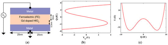
An isolated capacitor with Gd-doped HfO2 ferroelectric is shown in Figure 1a. Aluminum acts as a metal electrode. Gd-doped HfO2 was selected because its reported ferroelectric parameters provide suitable polarization characteristics and capacitance matching. The voltage-charge relation of an isolated (standalone) ferroelectric capacitor is given by Landau theory [8],
where and denote the charge and voltage associated with the ferroelectric capacitor, respectively. The parameters α and β correspond to the anisotropy coefficients of the ferroelectric layer (Table 1). The charge voltage curve has an S-shaped characteristic. The negative-slope region is the region of negative capacitance, which confirms instability [4,5,6]. However, it is a state of instability because of the double-well energy profile [4,8]. This energy landscape is that of a double-well potential,
Figure 1.
(a) Isolated FE capacitor; (b) charge vs. voltage characteristic of isolated Gd-doped HfO2 ferroelectric capacitor; (c) energy vs. charge characteristic of isolated Gd-doped HfO2 ferroelectric capacitor.
Table 1.
Anisotropy constants for ferroelectric material (Gd—gadolinium).
A distinct S-shaped charge-versus-voltage curve is shown in Figure 1b. The negative-slope region observed near its origin shows negative differential capacitance. This region corresponds to a condition where an increase in voltage gives a decrease in charge, which is physically unstable when the ferroelectric is isolated. The energy-charge characteristic is shown in Figure 1c. The double-well energy landscape is confirmation that the system has two stable minima separated by an unstable region. The concave region between the wells is the negative-capacitance state. Since the system has a natural tendency to enter one of the minima, the isolated ferroelectric cannot operate in a stable way in the negative-capacitance zone. These two figures put together determine that although there is an intrinsic negative capacitance in the ferroelectric material, it cannot be used directly without stabilization.
2.2. Dielectric-Only Structure (SiO2)
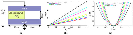
In Figure 2, the capacitance due to the cavity and the capacitance due to are added in parallel to form an equivalent dielectric capacitance,
For the dielectric-only structure shown in Figure 2, the applied voltage is developed across the equivalent dielectric capacitance formed by the parallel combination of the SiO2 layer and the cavity. Therefore, the voltage can be expressed as follows:
Figure 2.
(a) Dielectric-only structure; (b) charge vs. voltage characteristic of dielectric-only structure; (c) energy vs. charge characteristic of dielectric-only structure.
Similar dielectric-modulation mechanisms have been widely employed in capacitive biosensors and ferroelectric sensing platforms, whose electrical properties are directly related to the material filling it [1,2]. In the absence of biomolecules, the cavity is filled with air, which has a low dielectric constant. When biomolecules such as Keratin, gelatin, T7 or other analytes are present in the cavity, the effective dielectric constant increases and thus changes the electrical response of the structure. The dielectric capacitance of the cavity is thus given by
where is the dielectric constant of the filling material. The dielectric constants of the biomolecules are given in Table 2. Since capacitance is directly proportional to , any biomolecule that is introduced into the cavity creates a higher dielectric capacitance than the air-filled case [18]. Figure 2b displays a linear charge–voltage relationship for various cavity fillings. The slope increases systematically from air to higher-dielectric-constant biomolecules, indicating increased charge storage capabilities. This validates that the electrical response of the cavity is highly dependent on the biomolecular dielectric properties. The energy-charge profile of the dielectric region is shown in Figure 2c. All curves have a single parabolic shape, which confirms stable electrostatic behavior. However, the curvature differs depending on the dielectric constant, so that biomolecules with a higher k give a lower curvature, which corresponds to higher capacitance. These results establish that the cavity region is the sensing element, in which biomolecule presence directly modulates the dielectric capacitance.
Table 2.
Dielectric constants (K values).
2.3. FE–DE Heterostructure (Ferroelectric + Biomolecule-Filled Cavity)
The proposed cavity is intended for biomolecules dispersed in low-viscosity aqueous solutions rather than highly viscous bulk materials. Previous experimental studies have demonstrated the feasibility of detecting biomolecules in solution using nanogap capacitive sensors [18,19]. The present theoretical model considers the effective dielectric constant of the cavity, while viscosity, molecular transport, buffer effects, and electrical-double-layer screening require further experimental investigation. When the ferroelectric layer made of gadolinium is placed in series with the dielectric cavity, the system is the FE-DE heterostructure. In this configuration, the dielectric layer is not only a passive insulator but an active sensing region with a dielectric constant which varies with biomolecule occupancy. The choice of gadolinium (Gd)-doped HfO2 and was motivated by the capacitance-matching requirement of the FE-DE heterostructure. Since the sensitivity of the proposed biosensor is determined by the voltage developed across the dielectric region, achieving a close match between the ferroelectric capacitance and dielectric capacitance is essential for obtaining strong voltage amplification. For the selected layer thicknesses and device dimensions, the Gd/SiO2 combination provides a favorable capacitance-matching condition, resulting in enhanced voltage amplification and improved sensitivity to biomolecule-induced dielectric changes. Although other material combinations may be suitable for different geometries or thicknesses, the present combination was found to be optimal for the device configuration considered in this work [3,7]. The applied voltage is shared between the ferroelectric and the cavity as
and the equivalent capacitance of the heterostructure is given by
Here, dielectric capacitance, , is directly dependent on the biomolecule in the cavity. Therefore, any biomolecule-induced variation in dielectric constant alters the total capacitance of the FE-DE structure. Since both capacitors are connected in series, therefore, the charge across the ferroelectric layer remains identical to the charge in the dielectric. Using Kirchhoff’s voltage law, the relation can be written as ()
So, the total energy of the heterostructure can be expressed as the combined energy of the FE and DE capacitors ()
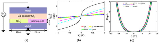
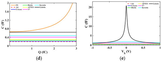
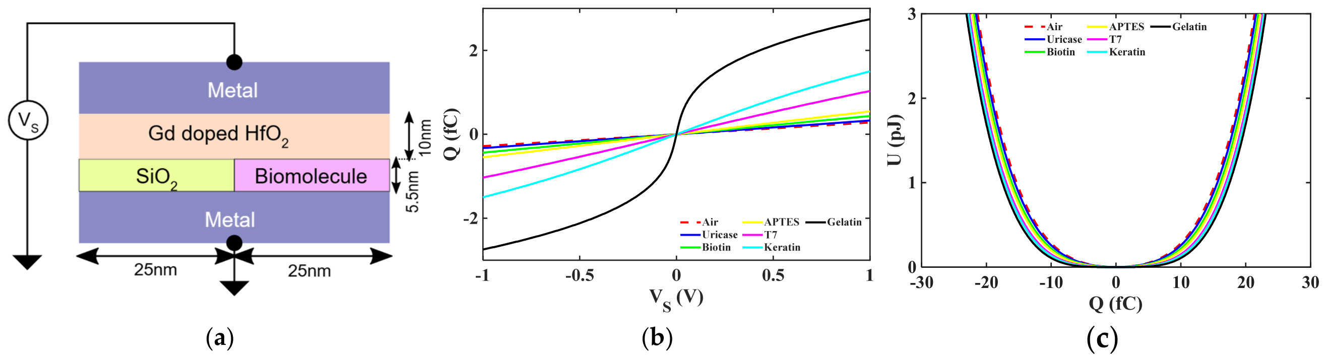
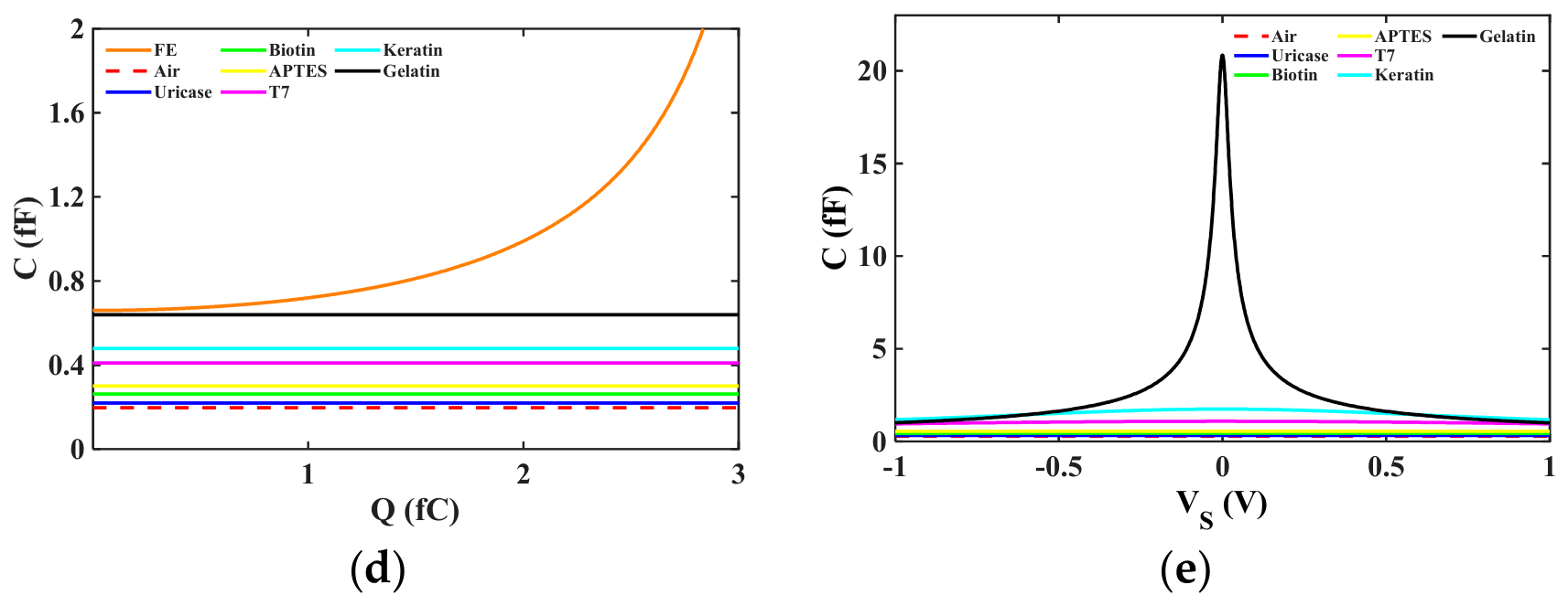
Figure 3b (Q-VS) shows that the unstable negative-slope region found for the isolated ferroelectric is eliminated with the introduction of the cavity. The dielectric cavity stabilizes the negative-capacitance behavior by contributing positive electrostatic energy into the circuit. The degree of stabilization is increased as the dielectric constant of the cavity is increased [4,6,8]. Figure 3c (UT-Q) shows the total energy profile of the coupled system. Compared to the double-well energy curve of the isolated ferroelectric, the energy landscape of the heterostructure is smoother and more flattened. This flattening happens because the cavity adds positive curvature, suppressing the unstable region of the ferroelectric. Figure 3d (CFE-Q) shows a capacitance enhancement when the biomolecules fill the cavity. As the dielectric constant goes from air to gelatin or Keratin, the dielectric capacitance is increased to nearly the magnitude of the ferroelectric capacitance. This improved condition of capacitance matching leads to a higher total equivalent capacitance. Figure 3e (CT-VS) further points out that the total capacitance of the heterostructure can exceed the dielectric capacitance alone near the matching region. This enhancement is because the ferroelectric is operating in a stabilized negative-capacitance regime. The higher the dielectric constant of the fillings, the higher the voltage redistribution, which is one of the reasons for sensing amplification. Overall, the FE-DE heterostructure can be physically viewed as a combination of a ferroelectric layer coupled with a dielectric cavity sensitive to biomolecules. The cavity filling determines the dielectric capacitance that in turn controls capacitance matching and energy stabilization. Therefore, the presence of biomolecules does not simply change the capacitance. It is actively controlling stabilization and amplification. The asymmetric half–half dielectric–cavity configuration was adopted considering fabrication simplicity and ease of cavity formation. In this biosensor, the sensing response is primarily determined by the effective biomolecule-filled cavity area and the resulting dielectric modulation rather than the exact cavity position within the dielectric region. Therefore, for a fixed cavity fraction, the sensor performance is expected to depend mainly on the capacitance variation introduced by the biomolecules. Although symmetric dielectric–cavity–dielectric configurations may also be considered, their performance would require separate optimization of cavity dimensions and capacitance-matching conditions.
Figure 3.
(a) FE–DE heterostructure; (b) Q-VS; (c) UT-Q; (d) CFE-Q; (e) CT-VS.
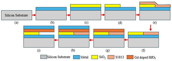
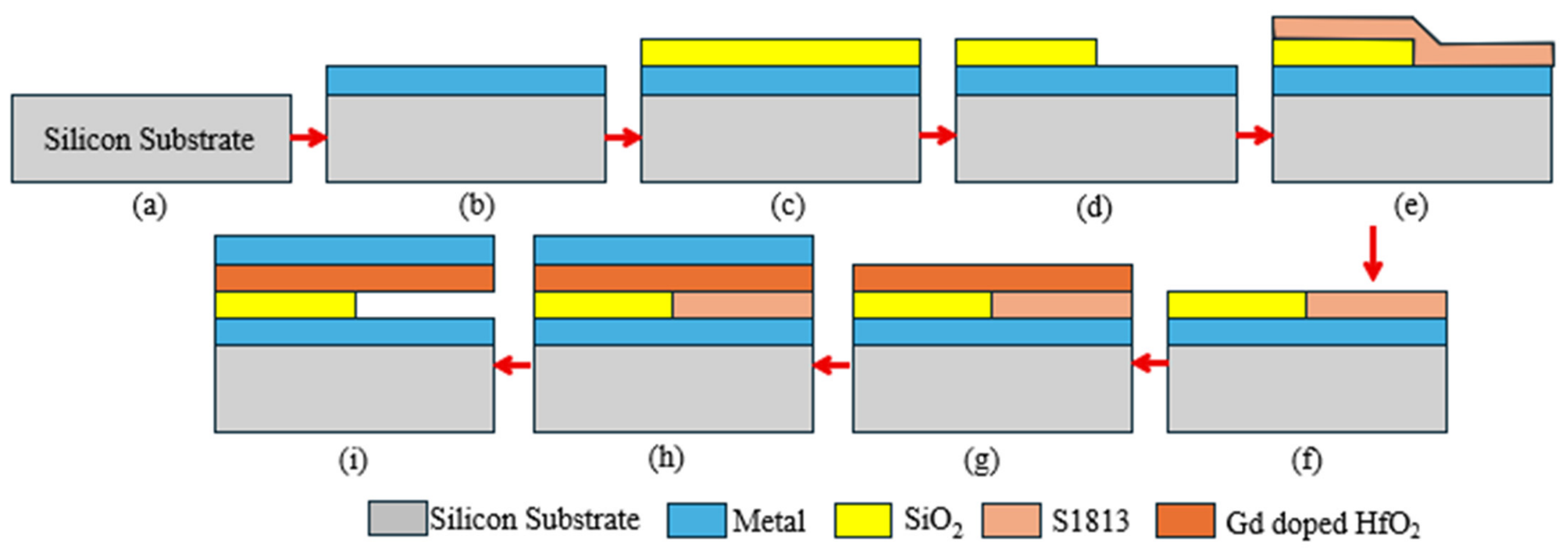
A feasible fabrication-integration plan is presented here to show the sensor realization processes. The initial wafer can be a silicon substrate Figure 4a. The metal can be deposited over the substrate, followed by 50 nm SiO2 deposition, as shown in Figure 4b,c. The SiO2 layer can be etched from half of the device to provide space for the cavity (Figure 4d), and the length of the SiO2 will become 25 nm. Anisotropic etching can be used for precise etching, followed by deposition and patterning of S1813 positive photoresist, as shown in Figure 4e,f. Furthermore, high-k gadolinium with a thickness of 50 nm can be deposited using the Sputtering technique [3,20], followed by metal deposition, as shown in Figure 4g,h. Finally, the device can be kept in acetone for few seconds to sacrificially remove the S1813 and create the cavity for biomolecule sensing, as shown in Figure 4i. The proposed fabrication-integration plan demonstrates the potential physical realization of the FE–DE biosensor. However, the present work is limited to a theoretical and physics-based evaluation.
Figure 4.
Proposed fabrication-process flow of the Gd-doped HfO2-based FE–DE heterostructure biosensor: (a) silicon substrate, (b) bottom metal deposition, (c) SiO2 deposition, (d) partial SiO2 etching for cavity formation, (e,f) S1813 photoresist deposition and patterning, (g) Gd-doped HfO2 ferroelectric layer deposition, (h) top metal deposition, and (i) sacrificial removal of S1813 to create the biomolecule sensing cavity.
2.4. Voltage Amplification Behavior
The voltage amplification factor is given as
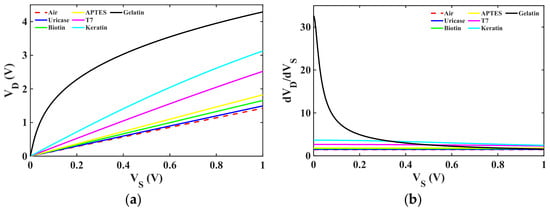
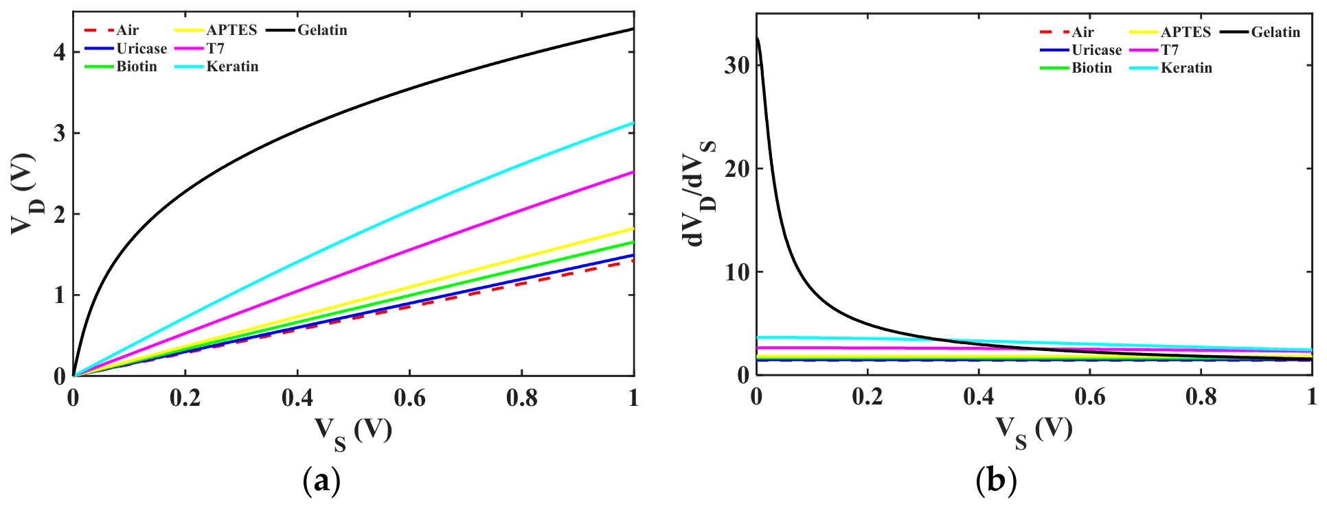
Voltage amplification takes place when the ferroelectric capacitance becomes comparable to the dielectric capacitance [7,21,22]. The biomolecules with high dielectric constants result in enhanced voltage amplification because of the better capacitance matching of the ferroelectric capacitance, , and effective dielectric capacitance, . Figure 5a on voltage amplification (VD vs. VS) shows the variation in the dielectric voltage, , with respect to the applied voltage, , for different biomolecules present in the cavity region. In the amplification region, the voltage across the dielectric layer rises more quickly than the applied supply voltage, which is an indication of intrinsic voltage gain in the FE-DE heterostructure. Materials such as Keratin and gelatin have a higher slope when compared to air and low-k biomolecules, which confirms that materials with high dielectric constants result in higher voltage amplification. Similar amplification behavior has been experimentally and theoretically reported in FE-DE heterostructures [5,7,23]. This is a result of the better matching of and allowing the system to operate closer to the stabilized negative-capacitance region and hence increasing the voltage transfer. Figure 5b shows the differential voltage amplification vs. , which is the instantaneous gain of the heterostructure. A gain value greater than one confirms the enhancement of the dielectric voltage in comparison to the applied voltage, demonstrating the amplification capability of the FE-DE system. The maximum gain occurs at lower voltages, where the capacitance-matching condition is the strongest. Biomolecules having a higher dielectric constant have a higher peak gain since they increase the dielectric capacitance, approaching the magnitude of the ferroelectric capacitance. As the applied voltage is increased, the gain gradually decreases, which indicates that the system is moved away from the optimum matching condition. This behavior confirms that the FE-DE heterostructure has the ability to translate small dielectric changes due to the presence of biomolecules into enhanced electrical response and is therefore very suitable for sensitive biosensing applications [24,25]. All results presented in Figure 2, Figure 3 and Figure 5 were obtained through MATLAB 2026a-based numerical simulations using the analytical FE-DE model described in Section 2. No experimental measurements were performed in the present work.
Figure 5.
(a) Voltage amplification; (b) differential voltage amplification.
2.5. Analysis for Different Biomolecule-Filling Percentages
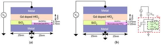
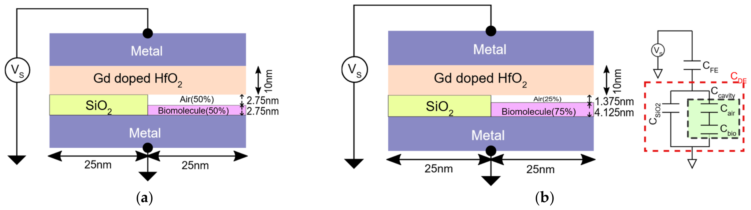
Different filling conditions were considered to analyze the sensing capability of the proposed FE-DE structure. The cavity region was modeled with different percentages of biomolecule filling. In addition to the case of an air-filled cavity discussed in Section 2.2 (0% biomolecule), intermediate filling conditions were introduced to represent realistic sensing scenarios. Specifically, the cavity was assumed to have 50% biomolecule and 50% air, 75% biomolecule and 25% air, and finally a fully occupied cavity corresponding to 100% biomolecule filling, which is discussed in Section 2.3. In these intermediate cases, the cavity capacitance is a function of the sum of the contributions of the air and biomolecule layers in the cavity region. The partial-filling configurations (50% and 75%) were considered to model intermediate biomolecule occupancy levels inside the sensing cavity. In practical biosensing applications, biomolecule immobilization is often incomplete due to finite analyte concentrations, non-uniform adsorption, and binding efficiency limitations. Therefore, partial cavity filling provides a useful framework for evaluating sensor response under realistic sensing conditions rather than assuming ideal full occupancy. Below are the models for 50% biomolecule and 75% biomolecule filling, respectively, and based on these partial-filling configurations, the dielectric region is represented by an equivalent capacitance network based on the physical structure of Figure 6a,b. When biomolecules partially fill the cavity, the remaining space in the cavity is filled with air. Since the air layer and the biomolecule layer are stacked vertically in the cavity region, they form a series capacitance combination, as mentioned in Equation (2).
Figure 6.
FE–DE heterostructure with partial biomolecule filling inside the cavity: (a) 50% biomolecule filling and (b) 75% biomolecule filling.
The layer and the cavity are placed side-by-side in the device structure. They have the same voltage applied to them and thus constitute a parallel capacitance combination. The effective dielectric capacitance becomes
This equivalent dielectric capacitance is series-connected with the ferroelectric layer to form the FE-DE heterostructure. The total capacitance of the device can therefore be represented as
where is the capacitance of the ferroelectric layer. This modeling approach enables us to incorporate the effect of various biomolecule-filling percentages within the cavity to the electrical behavior of the FE-DE heterostructure. As the content of biomolecules increases, the dielectric constant of the cavity region increases, which will modify the effective dielectric capacitance and thus will alter the voltage distribution in the device. Voltage amplification occurs when the magnitude of the negative ferroelectric capacitance approaches the dielectric capacitance,
Under this capacitance-matching condition , the denominator becomes small, resulting in a larger voltage drop across the dielectric layer. Small variations in dielectric capacitance caused by biomolecule binding produce amplified voltage changes at the output. This phenomenon forms the basis of the enhanced sensing response in the proposed FE-DE biosensor [7,8].
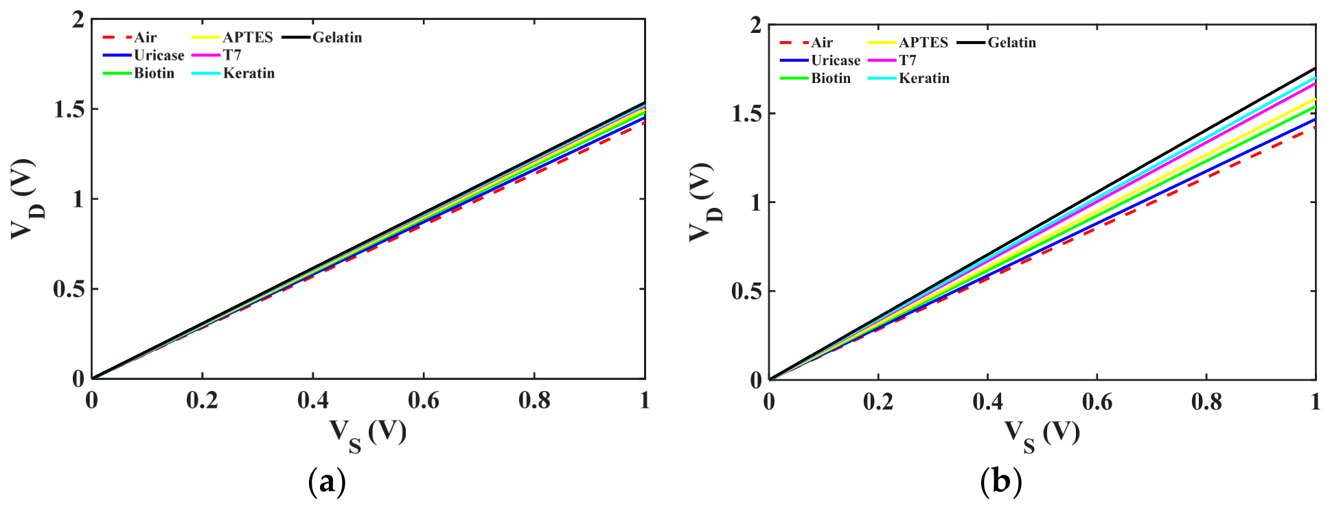
Figure 7 shows the voltage amplification characteristics for 50% and 75% cavity filling. In both cases, the output voltage increases linearly with the applied source voltage, confirming stable FE-DE operation. The amplification effect becomes more pronounced as the filling percentage increases from 50% to 75%, indicating that larger biomolecule occupancy strengthens the dielectric modulation and improves the electrical response of the FE-DE biosensor. The series-layer model approximates partial cavity occupancy. Actual biomolecule adsorption may be lateral and non-uniform, potentially producing higher capacitance and sensitivity. Realistic adsorption patterns require spatial analysis incorporating surface chemistry and fringing fields.
Figure 7.
(a) Voltage amplification with 50% biomolecule filling; (b) voltage amplification with 75% biomolecule filling.
2.6. Biosensor Sensitivity Analysis
The sensing ability of the proposed FE-DE heterostructure was evaluated by calculating the sensitivity of the device for various biomolecules in the cavity region. Sensitivity is the degree of change in the electrical response of the device due to the presence of biomolecules. Here, sensitivity is determined by measuring the variation in the dielectric voltage response when the percentage of biomolecule filling inside the cavity is increased. Sensitivity is calculated as the relative change in dielectric voltage with respect to the air-filled cavity condition, given by
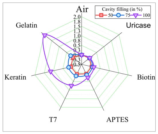
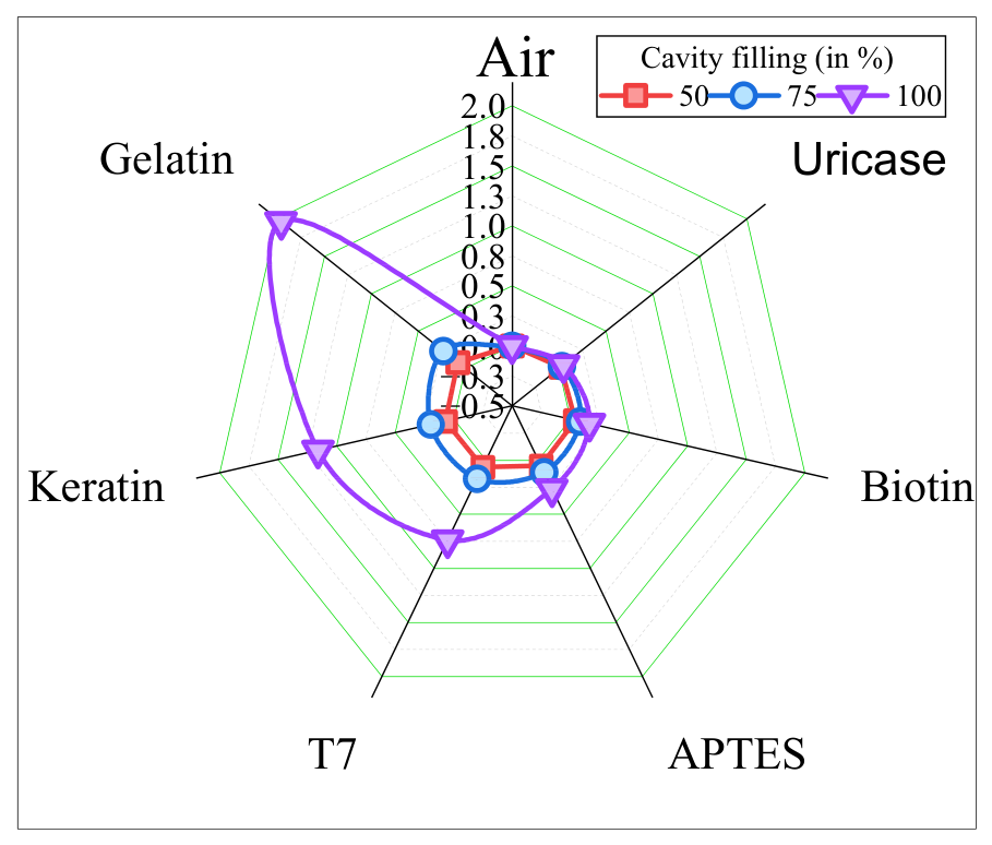
Figure 8 summarizes the values of the sensitivity obtained for different biomolecules at three cavity-filling conditions: 50%, 75% and 100% biomolecule occupancy. The dielectric constant K of each biomolecule significantly influences the total sensitivity for the structure. Materials having greater dielectric constants yield greater modulation in the effective dielectric capacitance of the cavity and hence yield a greater change in voltage response [1,26]. From the figure it is observed that the sensitivity consistently increases as the dielectric constant of the biomolecule increases. For example, air with a dielectric constant of K = 1 produces almost no change in sensitivity with different filling percentages. In contrast, biomolecules like Keratin and gelatin, which have much higher dielectric constants, result in much larger values of sensitivity. This trend shows that the coupling between the ferroelectric and the dielectric layers is increased by higher-dielectric-constant biomolecules, thus increasing the electrical response. Another important observation is that the sensitivity is enhanced by an increase in the biomolecule occupancy within the cavity. For most biomolecules, the values at 100% filling are much higher than the values at 50% or 75% filling. This behavior confirms that the sensing mechanism is directly related to the dielectric modulation introduced by the biomolecules. As the cavity is filled with more biomolecules, the effective dielectric constant of the sensing region is enhanced, which results in better capacitance matching and a higher voltage response of the FE-DE heterostructure. Overall, the results obtained from the sensitivity tests prove that the structure being proposed is capable of being used for distinguishing biomolecules by their dielectric properties [2,27]. The high sensitivity dependence both on the dielectric constant and the cavity occupancy underscores the potential of the FE-DE heterostructure for highly sensitive biosensing applications.
Figure 8.
Sensitivity variation of the FE-DE biosensor with dielectric constant for different cavity filling percentages.
2.7. Integration of FE–DE Biosensor with NMOS for Subthreshold Swing Improvement
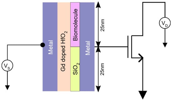
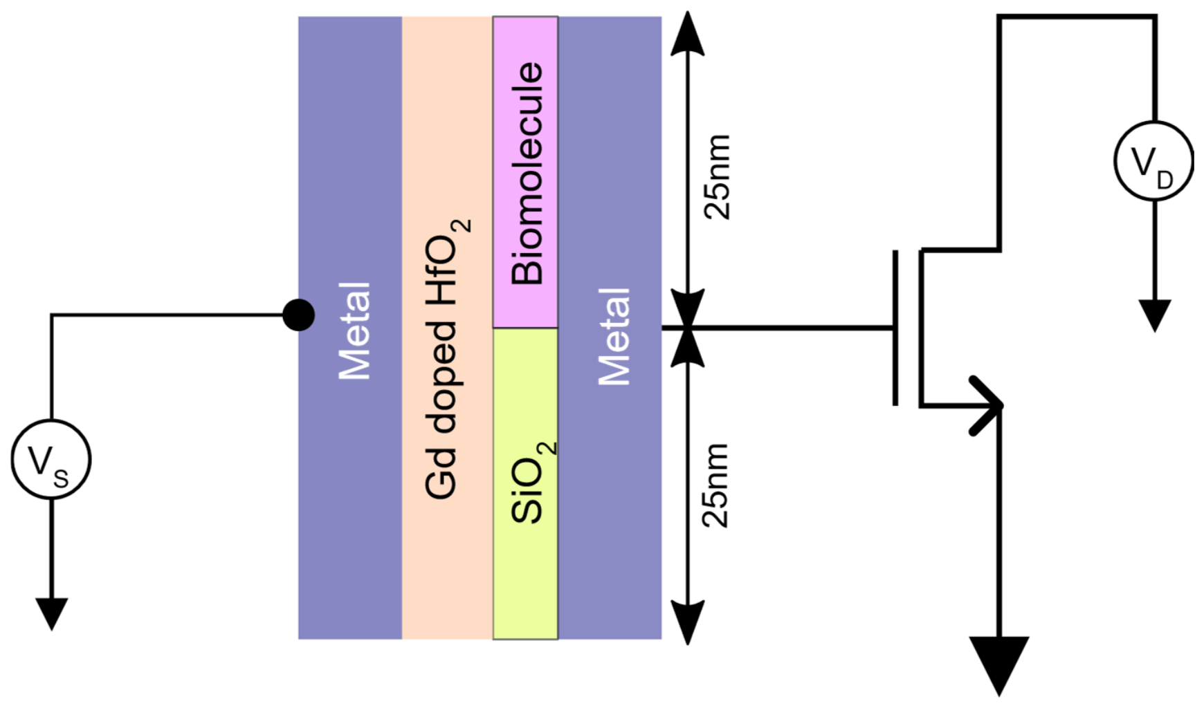
The practical applicability of the proposed FE–DE biosensor structure is evaluated by applying the dielectric voltage response obtained from the – characteristics as the gate input of an NMOS transistor. The goal of this integration is to examine the possibility of reaching subthreshold swing values lower than the conventional thermal limit of 60 mV/decade [4,12]. The circuit configuration used for this analysis is shown in the simulation setup where the amplified dielectric voltage generated by the ferroelectric–dielectric heterostructure drives the gate terminal of an NMOS transistor implemented in 50 nm CMOS technology [9,28,29]. In a conventional MOS transistor, the subthreshold swing is fundamentally limited by thermal voltage and is given by
at room temperature. However, if a stabilized negative-capacitance ferroelectric capacitor is connected to the gate of the transistor, the effective gate voltage amplification alters this relation [4,8]. The ferroelectric–dielectric heterostructure enhances the internal voltage applied on the MOS gate so that the potential in the channel can rise faster than the external supply voltage. In this work, the voltage amplification behavior obtained from the vs. characteristics (Section 2.4, Figure 5a) of the FE–DE biosensor was used as input data of the NMOS gate. The data set obtained from the voltage amplification curves is for different cases of biomolecules in the cavity region. A 50 nm NMOS transistor was used to investigate the practical effect of the proposed FE–DE biosensor structure [9,30,31]. As the amplified dielectric voltage is applied to the NMOS gate, the channel potential rises faster than the applied supply voltage. This has the effect of lowering the gate voltage needed to control the drain current in the subthreshold region. As a result, the drain current has a steeper exponential increase, and, therefore, the effective subthreshold swing is less than the conventional limit of 60 mV/decade [18,32,33].
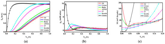
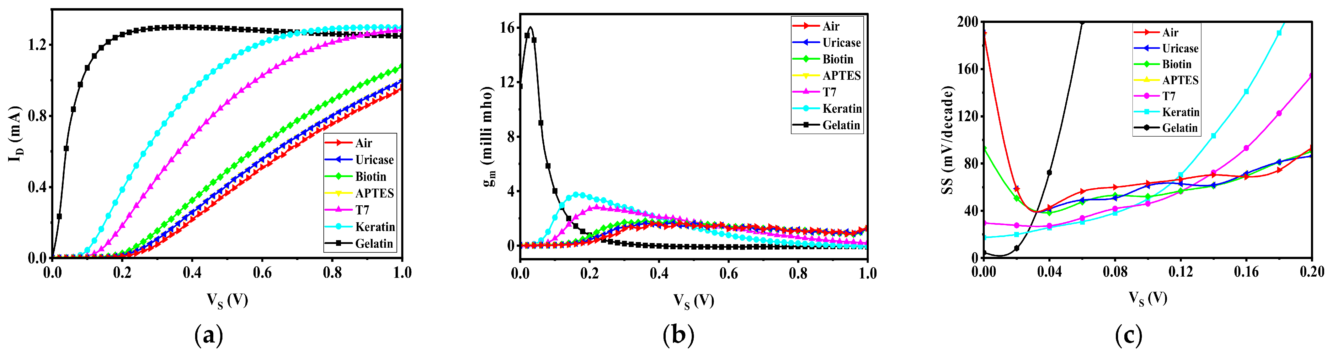
The voltage data extracted from the – curves for various biomolecules were taken and used as input data sets in the NMOS simulation, as illustrated in Figure 9. Using these data sets, the corresponding drain current () and transconductance () characteristics were obtained and plotted. Figure 10a shows the variation in drain current, , with supply voltage, . These curves show that biomolecules with higher dielectric constants generate stronger gate voltage amplification and, hence, earlier turn-on of the transistor and a steeper increase in drain current. Biomolecules like gelatin and Keratin produce much higher current levels compared to air-filled cavities because of the increased dielectric capacitance and better voltage coupling in the FE–DE structure. The transconductance versus characteristics are shown in Figure 10b for the same biomolecule conditions. Transconductance represents the variation in drain current with respect to gate voltage and is given by
These results show that when biomolecules have a higher dielectric constant, the transconductance values are larger in the lower voltage region. This is a consequence of the fact that the combination of the FE and DE heterostructures enhances the gate voltage applied to the transistor, and so the channel conductance increases faster. Therefore, the device has better switching behavior and higher electrical response. To assess the switching behavior of the NMOS device controlled by the output of the FE-DE biosensor, the subthreshold switch (SS) was extracted from the simulated drain-current characteristics. Subthreshold swing represents the gate voltage required to vary the drain current by one decade and is defined as
Figure 9.
Simulation setup for evaluating the effect of FE–DE biosensor voltage amplification on NMOS transistor characteristics using a 50 nm NMOS.
Figure 10.
(a) Variation in drain current, , with supply voltage, , and (b) transconductance, , versus supply voltage, , for different biomolecules when the FE–DE biosensor output drives a 50 nm NMOS transistor. (c) Subthreshold swing (SS) versus gate voltage, , for different biomolecules when the FE–DE biosensor output drives a 50 nm NMOS transistor.
In conventional low-temperature (room-temperature)-operating conventional MOS transistors, the theoretical limit to the subthreshold swing is 60 mV/decade, which is due to the thermionic emission of carriers across the channel barrier. Figure 10c presents the variation in subthreshold swing with gate voltage, , for different biomolecules present inside the cavity of the FE–DE biosensor. The results show that the combination of the ferroelectric–dielectric heterostructure and NMOS transistor greatly enhances the switching characteristics of the device. In the lower voltage region, several biomolecule cases have subthreshold swing values lower than the conventional 60 mV/decade limit, demonstrating the effect of voltage gain produced by the stabilized negative-capacitance effect of the ferroelectric layer. Among the biomolecules, materials with higher dielectric constants yield higher voltage amplification in the FE–DE heterostructure [4,8,18]. This amplification amplifies the effective gate control over the channel potential, so that the drain current rises faster with a smaller variation in the applied gate voltage. As a result, the device has low subthreshold swing and better switching efficiency. In contrast, the air-filled cavity case exhibits larger SS values because of the small dielectric constant and low voltage amplification. Biomolecules such as Keratin, T7 and APTES exhibit better switching behavior with SS values close to or below the thermal limit in certain operating regions. These results validate that the presence of biomolecules not only changes the dielectric properties of the sensing cavity but also improves the transistor switching behavior by the negative-capacitance effect. Hence, the SS characteristics prove that the FE-DE biosensor integrated with an MOS transistor can realize steeper switching slopes and higher energy efficiency, which makes the proposed structure promising for low-power biosensing and next-generation electronic devices. Various advanced transistor architectures, including double-gate, FinFET, SOI and gate-all-around devices, have been explored to improve electrostatic control and switching performance [31,32,33,34,35]. The present work is compared with other reported biosensors in Table 3. Since the reported studies quantify sensing responses using different electrical parameters, their numerical sensitivity values are not directly comparable. The present theoretical analysis demonstrates a maximum dielectric-voltage sensitivity of 1.9632 (196.32%) for gelatin at 100% cavity filling.
Table 3.
Comparison of the present work with representative biosensors reported in the literature.
3. Conclusions
This work studies a gadolinium (Gd)-doped HfO2-based FE–DE heterostructure for biosensing applications. Interaction between the ferroelectric and dielectric layers stabilizes the negative-capacitance behavior and results in capacitance enhancement together with intrinsic voltage amplification. The sensing mechanism is based on the changes in the dielectric constant of the cavity region upon the addition of biomolecules. Different biomolecules having different dielectric constants were investigated under various cavity-filling conditions (0%, 50%, 75% and 100%). The results indicate that an alteration of the dielectric environment alters the effective capacitance of the heterostructure, hence causing measurable changes in voltage amplification. Sensitivity analysis verifies that biomolecules with higher dielectric constants generate higher electrical responses. To further test the effect of this amplification, the output voltage of the FE–DE biosensor was used on the gate of a 50 nm NMOS transistor. The resulting transistor characteristics exhibit improved switching behavior and the potential to obtain subthreshold swing values lower than the conventional 60 mV/decade limit. These results show that the proposed FE-DE heterostructure is a promising method for fabricating high-sensitivity and low-power biosensing devices. The proposed FE–DE heterostructure biosensor can be used in biomedical diagnostics for the detection of biomolecules such as proteins, enzymes and DNA due to dielectric variations in the sensing cavity. Due to the intrinsic voltage amplification capability of the device, it is suitable for low-power and portable diagnostic systems. The integration of the biosensor with complementary metal-oxide-semiconductor (CMOS) technology also allows for the development of small bioelectronic sensing platforms. Such systems can be applied in wearable health-monitoring devices, environmental sensing and lab-on-chip diagnostic applications. Additionally, the voltage amplification behavior of the FE-DE structure can support the development of steep-slope, energy-efficient electronic devices. The present work is a simulation-based proof-of-concept study. Experimental validation, including transistor subthreshold characteristics and fabrication-level verification, remains part of future work. It should be noted that the present analysis is based on an ideal parallel-plate capacitance model and does not explicitly account for fringing fields, edge effects, or other finite-dimension electrostatic phenomena. For practical nanoscale implementations, such non-ideal effects may contribute to the overall capacitance and slightly alter the quantitative sensor response. Nevertheless, the present model provides a useful first-order framework for understanding the FE-DE voltage amplification mechanism and biomolecule-induced dielectric modulation. A more comprehensive analysis incorporating fringing-field effects will be considered in future work.
Author Contributions
S.K. (Shrikrishna Kulkarni), B.A., P.M.: Conceptualization, Data curation, Formal analysis, Investigation, Methodology, Resources, Software, Supervision, Validation, Visualization, Writing—original draft, Writing—review and editing, P.M., B.A., Y.N., S.K. (Sampath Kumar), P.K.: Formal analysis, Validation, Visualization, Writing—review and editing. All authors have read and agreed to the published version of the manuscript.
Funding
Open access funding was provided by the Manipal Academy of Higher Education, Manipal.
Data Availability Statement
The data analyzed in this study can be obtained from the corresponding author upon reasonable request.
Acknowledgments
Shrikrishna Kulkarni, Bhaskar Awadhiya, Yashwanth Nanjappa, Sampath Kumar, Praveen Kumar, and Pramod Martha acknowledge the Manipal Academy of Higher Education for support in obtaining the research findings.
Conflicts of Interest
The authors declare no conflicts of interest.
References
- Deng, C.; Zhang, Y.; Yang, D.; Zhang, H.; Zhu, M. Recent Progress on Barium Titanate-Based Ferroelectrics for Sensor Applications. Adv. Sens. Res. 2024, 3, 2300168. [Google Scholar] [CrossRef] [Scilit]
- Gao, W.; Zhu, Y.; Wang, Y.; Yuan, G.; Liu, J.-M. A review of flexible perovskite oxide ferroelectric films and their application. J. Mater. 2020, 6, 1–16. [Google Scholar] [CrossRef] [Scilit]
- Mikolajick, T.; Slesazeck, S.; Mulaosmanovic, H.; Park, M.H.; Fichtner, S.; Lomenzo, P.D.; Hoffmann, M.; Schroeder, U. Next generation ferroelectric materials for semiconductor process integration and their applications. J. Appl. Phys. 2021, 129, 100901. [Google Scholar] [CrossRef] [Scilit]
- Jain, A.; Alam, M.A. Stability Constraints Define the Minimum Subthreshold Swing of a Negative Capacitance Field-Effect Transistor. IEEE Trans. Electron Devices 2014, 61, 2235–2242. [Google Scholar] [CrossRef] [Scilit]
- Khan, A.I. On the Microscopic Origin of Negative Capacitance in Ferroelectric Materials: A Toy Model. In Proceedings of the 2018 IEEE International Electron Devices Meeting (IEDM), San Francisco, CA, USA, 1–5 December 2018; IEEE: New York, NY, USA, 2018; pp. 9.3.1–9.3.4. [Google Scholar] [CrossRef] [Scilit]
- Khan, A.I.; Radhakrishna, U.; Chatterjee, K.; Salahuddin, S.; Antoniadis, D.A. Negative Capacitance Behavior in a Leaky Ferroelectric. IEEE Trans. Electron Devices 2016, 63, 4416–4422. [Google Scholar] [CrossRef] [Scilit]
- Awadhiya, B.; Kondekar, P.N.; Meshram, A.D. Passive voltage amplification in non-leaky ferroelectric–dielectric heterostructure. Micro Nano Lett. 2018, 13, 1399–1403. [Google Scholar] [CrossRef] [Scilit]
- Wong, J.C.; Salahuddin, S. Negative Capacitance Transistors. Proc. IEEE 2019, 107, 49–62. [Google Scholar] [CrossRef] [Scilit]
- Müller, J.; Böscke, T.S.; Müller, S.; Yurchuk, E.; Polakowski, P.; Paul, J.; Martin, D.; Schenk, T.; Khullar, K.; Kersch, A.; et al. Ferroelectric hafnium oxide: A CMOS-compatible and highly scalable approach to future ferroelectric memories. In Proceedings of the 2013 IEEE International Electron Devices Meeting, Washington, DC, USA, 9–11 December 2013; IEEE: New York, NY, USA, 2013; pp. 10.8.1–10.8.4. [Google Scholar]
- Böscke, T.S.; Müller, J.; Braeuhaus, D.; Schröder, U.; Böttger, U. Ferroelectricity in hafnium oxide thin films. Appl. Phys. Lett. 2011, 99, 102903. [Google Scholar] [CrossRef] [Scilit]
- Li, S.; Zhou, D.; Shi, Z.; Hoffmann, M.; Mikolajick, T.; Schroeder, U. Involvement of unsaturated switching in the endurance cycling of Si-doped HfO2 ferroelectric thin films. Adv. Electron. Mater. 2020, 6, 2000264. [Google Scholar] [CrossRef] [Scilit]
- Park, M.H.; Lee, Y.H.; Kim, H.J.; Kim, Y.J.; Moon, T.; Kim, K.D.; Müller, J.; Kersch, A.; Schroeder, U.; Mikolajick, T.; et al. Ferroelectricity and antiferroelectricity of doped thin HfO2-based films. Adv. Mater. 2015, 27, 1811–1831. [Google Scholar] [CrossRef] [Scilit] [PubMed]
- Starschich, S.; Menzel, S.; Böttger, U. Evidence for oxygen vacancies movement during wake-up in ferroelectric hafnium oxide. Appl. Phys. Lett. 2016, 108, 032903. [Google Scholar] [CrossRef] [Scilit]
- Lomenzo, P.D.; Li, S.; Pintilie, L.; Istrate, C.M.; Mikolajick, T.; Schroeder, U. Memory Window Enhancement in Antiferroelectric RAM by Hf Doping in ZrO2. IEEE Electron Device Lett. 2022, 43, 1447–1450. [Google Scholar] [CrossRef] [Scilit]
- Narang, R.; Saxena, M.; Gupta, M. Modeling and simulation investigation of sensitivity of symmetric split gate junctionless FET for biosensing application. IEEE Sens. J. 2017, 17, 4853–4861. [Google Scholar] [CrossRef] [Scilit]
- Gao, H.; Shao, Y.; Shi, R.; Liu, Y.; Zhu, J.; Liu, J.; Zhu, Y.; Zhang, J.; Li, L.; Hu, X. Effect of few-layer Ti3C2T x supported nano-Ni via self-assembly reduction on hydrogen storage performance of MgH2. ACS Appl. Mater. Interfaces 2020, 12, 47684–47694. [Google Scholar] [CrossRef] [Scilit] [PubMed]
- Schroeder, U.; Park, M.H.; Mikolajick, T.; Hwang, C.S. The fundamentals and applications of ferroelectric HfO2. Nat. Rev. Mater. 2022, 7, 653–669. [Google Scholar] [CrossRef] [Scilit]
- Meghna Bapat, K.; Bhaskar, A.; Yashwant, N. Enhancing Voltage Amplification in FE-DE Heterostructure with Multiple Dielectrics. In Proceedings of the 2024 IEEE International Conference on Distributed Computing, VLSI, Electrical Circuits and Robotics (DISCOVER), Mangalore, India, 18–19 October 2024; IEEE: New York, NY, USA, 2024; pp. 164–170. [Google Scholar] [CrossRef] [Scilit]
- Yi, M.; Jeong, K.-H.; Lee, L.P. Theoretical and experimental study towards a nanogap dielectric biosensor. Biosens. Bioelectron. 2005, 20, 1320–1326. [Google Scholar] [CrossRef] [Scilit] [PubMed]
- Kobayashi, M.; Hiramoto, T. On device design for steep-slope negative-capacitance field-effect-transistor operating at sub-0.2V supply voltage with ferroelectric HfO2 thin film. AIP Adv. 2016, 6, 025113. [Google Scholar] [CrossRef] [Scilit]
- Saribal, Z.; Kemp, C.; Verrelli, E.; Iles, A.; Pamme, N.; Adawi, A.M.; Kemp, N.T. A label-free aptamer-based nanogap capacitive biosensor with greatly diminished electrode polarization effects. Phys. Chem. Chem. Phys. 2019, 21, 681–691. [Google Scholar] [CrossRef] [Scilit] [PubMed]
- Rahi, S.B.; Tayal, S.; Upadhyay, A.K. A review on emerging negative capacitance field effect transistor for low power electronics. Microelectron. J. 2021, 116, 105242. [Google Scholar] [CrossRef] [Scilit]
- Tekleab, D. Device Performance of Silicon Nanotube Field Effect Transistor. IEEE Electron Device Lett. 2014, 35, 506–508. [Google Scholar] [CrossRef] [Scilit]
- Taur, Y.; Buchanan, D.A.; Chen, W.; Frank, D.J.; Ismail, K.E.; Lo, S.-H.; Sai-Halasz, G.A.; Viswanathan, R.G.; Wann, H.-J.C.; Wind, S.J.; et al. CMOS scaling into the nanometer regime. Proc. IEEE 1997, 85, 486–504. [Google Scholar] [CrossRef] [Scilit]
- El-Moghazy, A.Y.; Wisuthiphaet, N.; Yang, X.; Sun, G.; Nitin, N. Electrochemical biosensor based on genetically engineered bacteriophage T7 for rapid detection of Escherichia coli on fresh produce. Food Control 2022, 135, 108811. [Google Scholar] [CrossRef] [Scilit]
- Ratnesh, R.K.; Goel, A.; Kaushik, G.; Garg, H.; Chandan; Singh, M.; Prasad, B. Advancement and challenges in MOSFET scaling. Mater. Sci. Semicond. Process. 2021, 134, 106002. [Google Scholar] [CrossRef] [Scilit]
- Ieong, M.; Wong, H.-S.P.; Nowak, E.; Kedzierski, J.; Jones, E.C. High performance double-gate device technology challenges and opportunities. In Proceedings of the International Symposium on Quality Electronic Design, San Jose, CA, USA, 18–21 March 2002; IEEE: New York, NY, USA, 2002; pp. 492–495. [Google Scholar] [CrossRef] [Scilit]
- Reddy, M.N.; Panda, D.K. A Comprehensive Review on FinFET in Terms of its Device Structure and Performance Matrices. Silicon 2022, 14, 12015–12030. [Google Scholar] [CrossRef] [Scilit]
- Park, J.-T.; Colinge, J.-P.; Diaz, C.-H. Pi-Gate SOI MOSFET. IEEE Electron Device Lett. 2001, 22, 405–406. [Google Scholar] [CrossRef] [Scilit]
- Kaur, R.; Singh, B. Comparative Study of Single and Double Gate All Around Cylindrical FET Structures for High-K Dielectric Materials. Trans. Electr. Electron. Mater. 2021, 22, 509–514. [Google Scholar] [CrossRef] [Scilit]
- Sharma, A. Analysis of Low Frequency Drain Current Model for Silicon Nanowire Gate-All-Around Field Effect Transistor. Int. J. Hybrid Inf. Technol. 2014, 7, 326–336. [Google Scholar] [CrossRef] [Scilit]
- Sood, H.; Srivastava, V.M.; Singh, G. Advanced MOSFET Technologies for Next Generation Communication Systems—Perspective and Challenges: A Review. J. Eng. Sci. Technol. Rev. 2018, 11, 180–195. [Google Scholar] [CrossRef] [Scilit]
- Tiwari, P.K.; Kumar, M.; Naik, R.S.; Saramekala, G.K. Analog and radio-frequency performance analysis of silicon-nanotube MOSFETs. J. Semicond. 2016, 37, 064003. [Google Scholar] [CrossRef] [Scilit]
- Fahad, H.M.; Hussain, M.M. Are Nanotube Architectures More Advantageous Than Nanowire Architectures For Field Effect Transistors? Sci. Rep. 2012, 2, 475. [Google Scholar] [CrossRef] [Scilit] [PubMed]
- Bhaskar Awadhiya, S.; Yadav, Y.; Nanjappa, A.; Pahuja, S.; Yadav, S.; Agrawal, S. Passive Voltage Amplification in FE-FE-DE Heterostructure. IEEE Access 2024, 12, 43053–43061. [Google Scholar] [CrossRef] [Scilit]

Disclaimer/Publisher’s Note: The statements, opinions and data contained in all publications are solely those of the individual author(s) and contributor(s) and not of MDPI and/or the editor(s). MDPI and/or the editor(s) disclaim responsibility for any injury to people or property resulting from any ideas, methods, instructions or products referred to in the content. |
© 2026 by the authors. Licensee MDPI, Basel, Switzerland. This article is an open access article distributed under the terms and conditions of the Creative Commons Attribution (CC BY) license.