


Abstract
The von Neumann architecture faces a “memory wall” problem due to the physical separation of memory and processor, posing major challenges to energy efficiency and latency in the era of artificial intelligence. To overcome these bottlenecks, artificial synaptic devices inspired by biological systems have emerged as an important research direction. By integrating sensing and computing functions at the device level, these architectures provide a promising approach for the efficient processing of natural physical signals. Supported by advances in functional materials and artificial neural network (ANN) algorithms, artificial synaptic devices are capable of perceiving and processing various external stimuli, showing strong potential for applications in intelligent electronic skins, robotics, and edge computing. This review provides a comprehensive overview of recent advances in artificial synaptic devices, with particular emphasis on tactile and visual sensing applications. We discuss representative device types and operating mechanisms, analyze critical challenges from the perspectives of material engineering and functional integration, and further summarize potential solutions and future trends toward multimodal sensory–memory–computing systems.
1. Introduction
In the past half century, the evolution of computing technology has always revolved around a core contradiction: the exponential growth of data demand and the slow pace of improving underlying hardware energy efficiency. The von Neumann architecture, with its clear “memory–computing” separation logic, laid the foundation for modern computers, but also gave rise to the insurmountable “memory wall” problem. With the rapid development of applications such as artificial intelligence, the Internet of Things, autonomous driving and edge computing, the limitations of traditional architecture have become the main bottleneck in perception-intensive scenes. For example, autonomous driving cameras generate several GB of data per second, and some of the information is eventually discarded after undergoing analog-to-digital conversion, storage and digital processing. This “perception before thinking” mode not only wastes power consumption, but also leads to delays in key decisions. Therefore, the integration of sensing and computing has emerged as a disruptive paradigm. This emerging paradigm aims to mimic the information processing methods of biological systems, deeply integrating sensing and computing functions at the physical levels, opening up a technological revolution of “perception as computation”. This emerging integrated sensing–computing model greatly reduces data migration, demonstrating disruptive potential in terms of energy efficiency, speed, and integration. Among different technologies, artificial synaptic devices are a typical representative [1,2,3].
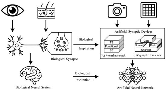
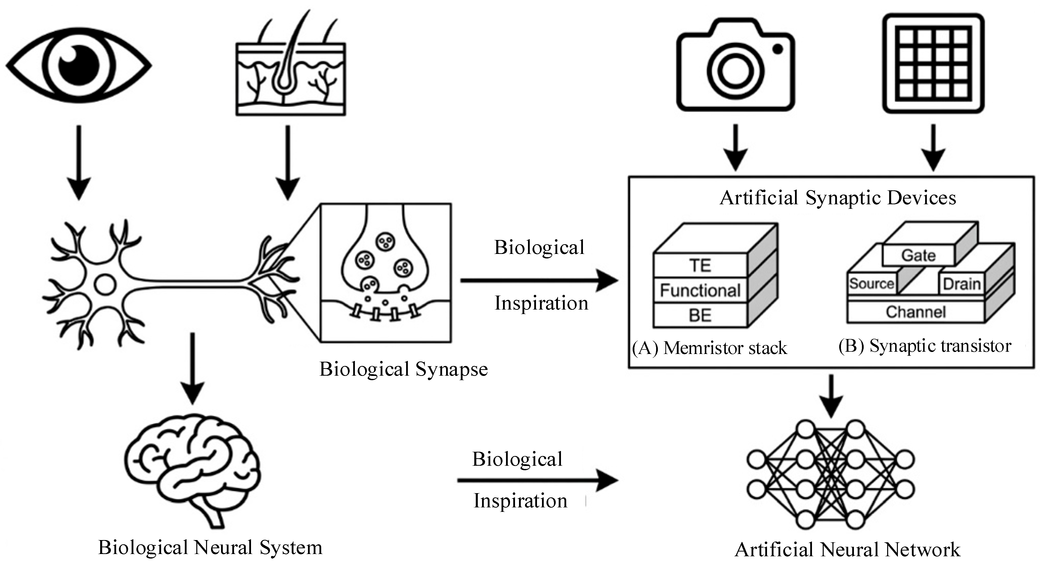
To clearly illustrate this bio-inspired paradigm, Figure 1 compares a biological sensory neural network with an artificial synaptic system. Biological systems process visual and tactile inputs through complex synaptic networks, which artificial architectures efficiently emulate using optical and pressure sensors coupled with synaptic devices (e.g., memristors and synaptic transistors) for integrated sensing and computing.
Figure 1.
Schematic comparison of biological sensory neural networks and bio-inspired artificial synaptic systems.
Human behavior is extremely complex and relies on sensory neural networks that are adaptive, plastic, and event-driven. This neural system can efficiently analyze multiple sensory cues while perceiving, in order to establish an accurate description of the environment. This provides important biological structural references for the study of integrated sensing and computing systems. Unlike the traditional hierarchical model of “perception first, transmission later, and calculation later”, artificial synaptic devices attempt to process information directly at the source of its generation, allowing data to be preliminarily calculated and filtered at the moment it is obtained. This architecture not only significantly reduces the energy consumption and latency caused by data processing but also enables computing units to process multimodal signals in complex environments under high-concurrency and low-power-consumption conditions, thus better meeting the needs of future intelligent applications [4,5,6]. It is worth noting that research on artificial synaptic devices is not an extension of a single discipline, but a deep intersection of materials, integrated circuits, artificial intelligence, and neuromorphic computing. In recent years, researchers have explored how to achieve the integration of sensing and computing on unified physical platforms through various approaches such as memristors, two-dimensional materials, and optoelectronic hybrid integration. At the same time, with the development of flexible electronics and new neural network algorithms, the application boundaries of artificial synaptic devices are constantly expanding, from traditional image recognition to multimodal scenarios such as tactile interaction, gas detection, and speech processing.
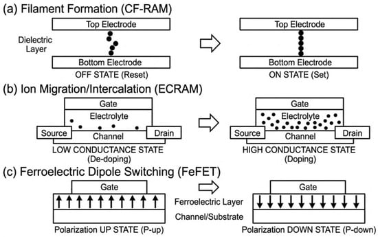
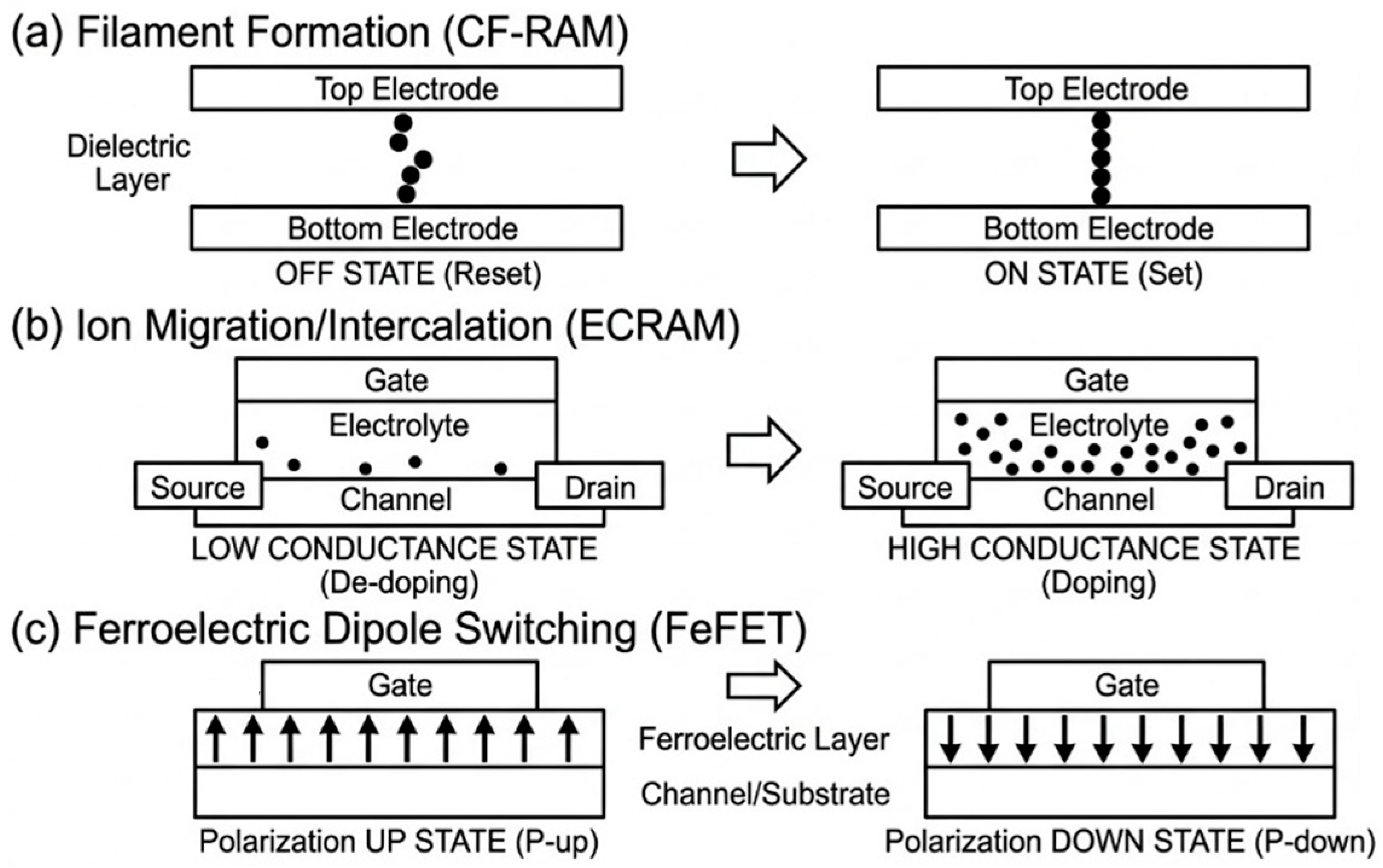
Before exploring specific applications, it is crucial to understand how nanoscale physical mechanisms govern artificial synaptic behaviors. The successful emulation of short-term (STP) and long-term plasticity (LTP) directly maps onto specific material dynamics. To clearly illustrate these concepts, Figure 2 provides a schematic overview of the three primary switching mechanisms. For instance, in memristors driven by conductive filament formation, the spontaneous rupture of unstable nanoscale filaments mimics STP’s rapid decay, whereas forming robust pathways establishes non-volatile LTP. In electrochemical transistors, fast, reversible ion migration at interfaces results in temporary STP, while deep ion intercalation ensures long-term LTP. Similarly, in ferroelectric devices, the intrinsic depolarization of ferroelectric domains drives STP, whereas the gradual accumulation of flipped domains under repeated pulses enables LTP. These fundamental physical processes form the indispensable hardware foundation for artificial synaptic plasticity.
Figure 2.
Schematic illustration of the primary physical mechanisms in artificial synaptic devices. (a) Conductive filament formation in memristive structures, showing the transition between the OFF (Reset) and ON (Set) states through filamentary dynamics. (b) Ion migration and intercalation in electrochemical systems, illustrating the doping and de-doping processes that modulate channel conductance. (c) Ferroelectric dipole switching in field-effect transistors, depicting the polarization-up (P-up) and polarization-down (P-down) states and the resulting surface charge accumulation.
This review focuses on tactile and visual artificial synaptic devices, while briefly discussing emerging progress in temperature, humidity, and magnetic field sensing. The key challenges, corresponding solutions, and future development trends are also discussed.
2. State of the Art
2.1. Tactile Synaptic Devices
In the human body, tactile signals are captured by various receptors densely distributed in the skin and then transmitted through nerve fibers to the spinal cord and brain for asynchronous, parallel, event-driven processing, ultimately forming a precise biological perception of object material, shape, softness, and slip. This process is efficient, low-power, and highly real-time. If traditional tactile sensors are used for signal acquisition, massive amounts of data will be generated. These massive amounts of raw data need to be continuously transmitted to the central processing unit, which poses a huge challenge to communication bandwidth. Artificial synaptic devices that integrate sensing and computing functions have become a hot topic in academic research in recent years. In artificial tactile synaptic devices, synaptic plasticity refers to the fact that the weights of synapses connected to neurons change with the time and frequency of external signal stimuli. Typically, synaptic plasticity is divided into short-term plasticity (STP) and long-term plasticity (LTP). In short-term plasticity, synaptic weights remain constant for short period of time at the millisecond level, mainly used for controlling signal transmission to postsynaptic neurons. In long-term plasticity, changes in synaptic weights will persist for longer periods of time, responsible for learning and memory functions. Advanced tactile sensors must have both STP and LTP functions so that tactile signal processing can mimic biological systems, thereby diversifying the functionality of tactile sensors.
In neuromorphic applications, sensors or transistors use synaptic weights to respond to complex, parallel, and multidimensional stimuli for information processing. So, the multi value and range of synaptic weights determine the overall performance of the neuromorphic system. Previous memristors, such as RRAM, could only exhibit limited weight values and could not generate continuously changing weights under external signal stimulation, limiting their application as synaptic devices. To overcome the limitations of traditional RRAM, researchers have explored ion migration-based devices. Gerasimov et al. proposed an evolvable organic electrochemical transistor (OECT) that operates in a mixed accumulation depletion state [7]. This device uses PETE-S as channel material. The gate serves as the presynaptic terminal, while the drain serves as the postsynaptic terminal. When receiving external stimuli, the amplitude and polarity of the gate voltage (VG) modulate the drain current (ID) accordingly. The synaptic weight is determined by the characteristics of the channel. The input of the gate is weighted by the channel conductance and is continually converted to an output current spike at the drain, which is proportional to the synaptic strength. Therefore, by controlling the input gate signal, the response intensity of OECT to stimuli can be adjusted within several orders of magnitude. Finally, OECTs were used to build a learning system, which realized Pavlovian conditioning, to prove its efficiency. Similarly utilizing ionic dynamics, Kim et al. introduced an intelligent haptic perception device (IHPD) which can switch between the operation of STP and LTP. The IHPD is composed of a polymer-based channel, gold source/drain electrodes, gate electrodes, a pyramid-patterned ion gel, and an indium tin oxide/polyethylene terephthalate (ITO/PET) film as the top electrode [8]. The application of IHPD in artificial electronic skin not only realizes the induction and transmission of external pressure signals, but also the learning and memory functions of pressure signal changes, which greatly enrich its functions. These representative devices generally rely on ion migration, diffusion, and electrochemical doping/dedoping processes to modulate channel conductance, thereby enabling continuously tunable synaptic weights and diverse plasticity behaviors. However, because their operation is inherently governed by ionic dynamics, their response speed and bandwidth are usually limited compared with purely electronic devices. In addition, many electrolyte-based implementations still face challenges in long-term stability, device uniformity, and large-scale integration, which remain important issues for practical neuromorphic edge-computing systems.
To construct complete sensory reflex systems, hybrid architectures have been developed. Kim et al. proposed an artificial afferent nerve including a resistive pressure sensor, organic ring oscillator, and synaptic transistor. The resistive pressure sensors consist of a conducting pyramid-structured elastomer which performs as a resistor between a carbon nanotube and Au electrodes [9]. This pressure sensor can sense pressure information ranging from 1 to 80 kPa. The ring oscillator converts pressure information into action potentials, which are then converted into postsynaptic currents using synaptic transistors. Synaptic transistors can be used to interface with biological efferent nerves to form complete single synaptic reflex arc. In the end, the artificial nerves are connected to the motor nerves, constructing a hybrid bioelectronic reflex arc to drive muscles, which can be applied in the fields of neural robots and neural prosthetics. The sensory neurons located within biological skin serve as bridge between the external physical world and the internal sensory neurons. Wan et al. demonstrated a neuromorphic tile processing system (NeuTap) [10]. The system consists of a resistive pressure sensor (receptors in sensory neuron), soft ionic cables (axon), and a synaptic transistor (information processing synapse). The pressure sensor first converts external pressure stimuli into voltage signals, which are transmitted to synaptic transistors through interface ion/electron coupling via an ionic cable. This work also demonstrates an event-driven approach. The system will only be activated when there is external pressure stimulation. The activated system can effectively extract spatial–temporal information from tactile features, thereby providing accurate tactile perception capabilities. By combining machine learning methods to train NeuTap, the system can achieve a perception and recognition accuracy of 99.6% for tactile information. These hybrid architectures elegantly demonstrate the feasibility of mimicking complex biological pathways—such as complete reflex arcs and event-driven spatiotemporal processing—by synergistically integrating distinct sensory, signal-conversion, and synaptic modules. However, such multi-component assemblies (e.g., separate pressure sensors coupled with discrete oscillators or ionic cables) may introduce additional hardware complexity and interconnect overhead. Moving from these proof-of-concept discrete systems toward densely integrated platforms therefore remains an important engineering challenge for scalable artificial electronic skin.
To avoid the packaging issues of ionic systems and the footprint issues of discrete circuits, solid-state ferroelectric materials offer a promising alternative. One-dimensional (1D) fibers made of organic materials have the characteristics of being soft, light, and flexible, and their processes are simple and compatible with many existing semiconductor processes. Therefore, they have received widespread attention in smart electronic textiles (e-textiles). Ham et al. studied and implemented 1D fiber-shaped multi-synapses. This synapse is composed of ferroelectric organic transistors, in which the ferroelectric transistors form multiple synaptic channels through an interlaced structure [11]. This multi-synapse has good scalability and maintains good performance and reliability even after thousands of repetitions of input stimulation under certain mechanical bending stress. Based on this device, an NOR-based textile array is built in. In MNIST and ECG experiments, a 1D multi-synapse achieved a recognition accuracy of up to 90% and 70%, respectively. Even under mechanical bending stress, the initial accuracy of the electrocardiogram mode remains within an error range of about 2%. This 1D synaptic structure provides an important direction for the development of e-textile neural networks for wearable neuromorphic electronic applications. In order to mimic the Merkel cell–neurite complexes in tactile organs, Lee et al. demonstrated a flexible, artificial, intrinsic–synaptic tactile sensory organ (AiS-TSO) [12]. The core of AiS-TSO is an organic synaptic transistor, which uses a ferroelectric nanocomposite of barium titanate nanoparticles and polyvinylidene fluoride trifluoroethylene as the gate dielectric. When feeling external pressure stimuli, due to ferroelectric dipole switching, post-synaptic current can be adjusted. A 2 × 2 sensor array is constructed using AiS-TSO, and its synaptic weights can be adjusted by changing the nanocomposite material of the gate dielectric layer, thereby achieving the memory function of tactile organs. These ferroelectric-driven architectures successfully integrate sensing and synaptic memory into a unified, flexible solid-state domain, effectively circumventing the electrolyte leakage and dehydration issues associated with ionic devices. By relying on ferroelectric dipole switching, they offer a robust intrinsic plasticity suitable for wearable artificial skin. Nevertheless, scaling these solid-state nanocomposites and fiber networks for practical applications introduces distinct material engineering challenges, primarily regarding ferroelectric fatigue over prolonged mechanical and electrical cycling, as well as the strict fabrication control required to ensure uniform nanoparticle dispersion and dense array alignment.
Among existing achievements, tactile–visual synapses are rarely applicable to real-time motion monitoring and healthcare systems. Based on a top-gate organic electrochemical transistor (OECT), Kim et al. designed an electrochemiluminescent tactile–visual synapse (ECL-TVS) [13]. ECL-TVS combined with an artificial neural network output feedback algorithm can achieve the monitoring of finger rehabilitation and electrocardiogram analysis. ECL-TVS adopts an electrochemical transistor structure, which includes an elastic top gate as a tactile receptor and an electrical synaptic channel formed between drain and source electrodes. Using a spiking neural network (SNN) at a power supply voltage of 3 V, the power consumption is only 34 μW, providing a convenient and effective platform for personalized medicine. This approach elegantly expands the traditional tactile sensory paradigm by incorporating real-time optical emission, providing a direct and intuitive visual feedback mechanism for in situ healthcare monitoring. Pushing this concept further to the system integration level, Xu et al. developed a self-powered visual–tactile human–machine interaction (VT-HMI) system by integrating a triboelectric nanogenerator (TENG) array with an InGaZnO nanowire synaptic transistor array. This integrated system successfully preprocessed dynamic tactile signals and mapped them into real-time, intuitive visual feedback via an LED array, achieving over 90% accuracy in trajectory recognition [14]. Consequently, balancing this intuitive visual output with the high-speed, high-frequency processing demands of advanced neuromorphic systems remains a crucial optimization target for future interactive electronics.
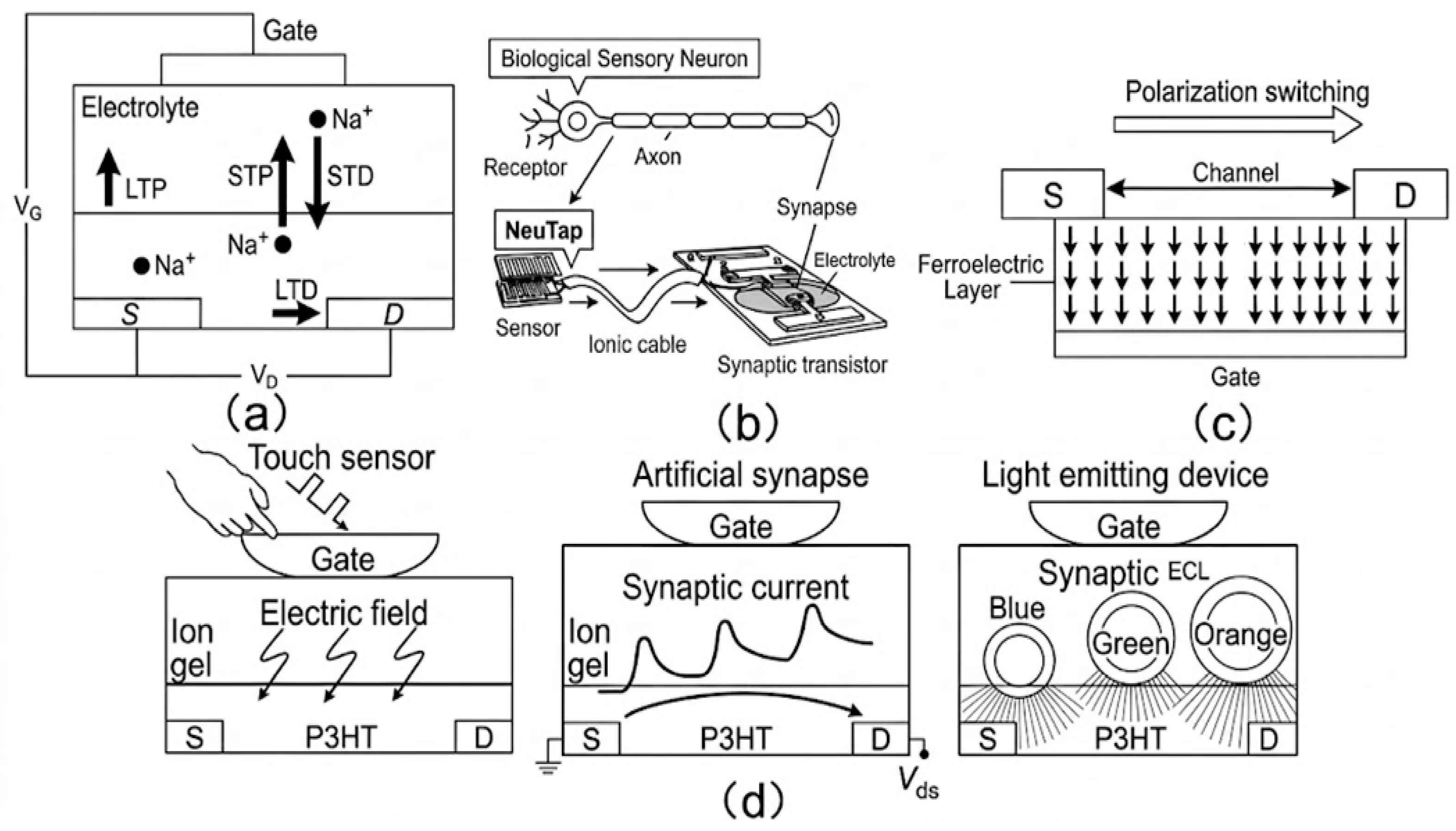
Overall, current tactile synaptic devices have evolved along several representative routes, including ionic/electrochemical devices, hybrid multi-component systems, solid-state ferroelectric devices, and multimodal tactile–visual synapses. Each route offers distinct advantages in synaptic plasticity, functional integration, and application scenarios. To facilitate a clearer comparison of their representative architectures and operating principles, the typical device configurations are schematically summarized in Figure 3. A summary and critical comparison of these representative categories is provided in Table 1.
Figure 3.
Representative architectures of tactile synaptic devices. (a) Ionic/electrochemical synaptic transistor. (b) Hybrid multi-component tactile synaptic system. (c) Solid-state ferroelectric synaptic device. (d) Tactile–visual integrated synaptic device.
Table 1.
Summary and critical comparison of representative tactile synaptic device categories.
2.2. Photonic Synaptic Devices
In the past 20 years, scholars have used different materials and adopted phase-change chalcogenides [15,16,17], metal–insulator–metal structures [18,19], and ferroelectric materials [20], as well as nanomaterial-based field-effect transistors [21,22], to develop a large number of electronic devices with synaptic functions. These devices mainly use electrical signals for communication and inevitably generate some losses during signal transmission and computation. Compared with electrical signals, optical signals theoretically have the advantages of infinite bandwidth and no interconnect power loss. Therefore, using optical communication to achieve artificial neuron synapses is a more effective solution. Based on their structural features and integration strategies, current photonic synaptic devices can be mainly divided into several categories.
To fully exploit the bandwidth of optical signals, realizing computation entirely within the optical domain is highly desired. Based on phase-change materials and integrated silicon nitride waveguides, Cheng et al. proposed a photonic synapse structure in the optical domain [23]. This photonic synapse can set synaptic weights by adjusting the number of light pulses sent along the waveguide, thus meeting the basic requirements of neural morphology calculation. Through simulation, it has been proven that the synapse has uniform electric field distribution, which enables the accurate setting of synaptic weights by adjusting the energy and duration of electrical pulses. An optical method was presented to modulate the synaptic weight based on the time delay between the pre- and post-neuron signals that can mimic the spike timing-dependent plasticity (STDP) rule in biological systems. This work proposes a new architecture that combines neuromorphic computing with photonic computing. While pure photonic waveguide architectures theoretically offer the highest bandwidths and zero electrical interconnect loss, they generally suffer from large spatial footprints, making them difficult to scale to ultra-dense integrated arrays.
Integrating optical sensing and non-volatile memory into a single physical footprint allows for in-sensor computing. Among various photonic synapse devices, non-volatile flash-based optical memory has the advantages of a short optical programming time, long-term storage, and linear plasticity, making it a strong competitor for achieving low-power, high parallel processing of artificial neural synapses. Chen et al. explored the physical effects of APbBr3 perovskite quantum dots (PQDs) on the photoresponsive properties of derived poly (3-hexylthiophene-2,5-diyl) (P3HT)/PQD-based optical memory, and constructed a photonic synapse with an excellent on/off current ratio [24]. This device realizes the pair-pulse facilitation, long-term plasticity, and multiple spike-dependent plasticity. It also has good linear plasticity and other functions. Light response experiments have shown that the energy consumption of each synaptic event is only 3 × 10⁻¹⁷ J. Due to the advantages of the narrow exciton binding energy, outstanding absorption properties, high stability, high charge carrier mobility, and long charge carrier lifetime of all organic perovskite CsPbBr3 quantum dots (QDs), it has become an important material choice for photonic memory. Wang et al. designed a heterogeneous photonic memory by combining inorganic perovskite quantum dots and flash memory structures [25]. Firstly, CsPbBr3 QDs exhibit excellent response characteristics to various wavelengths ranging from 365, 450, 520 to 660 nm. Secondly, the heterojunction formed between CsPbBr3 QDs and the semiconductor layer enables the programming and erasing functions of photonic memory. By adjusting the synaptic weights with different wavelengths of incident light, this photon flash memory also achieves the function of optical synapses. The device-level experimental results show that the photonic flash memory can perform artificial computing functions of STP, LTP, paired-pulse facilitation (PPF), paired-pulse depression (PPD), and spike rate-dependent plasticity. These optoelectronic non-volatile memories successfully achieve ultra-low energy consumption and compact sensing–memory integration at the single-device level. However, their ultimate operating speed is often constrained by the relatively slow charge-trapping and carrier-storage dynamics associated with non-volatile state retention.
To process complex environmental data beyond the visible spectrum, broadband and spectrally selective optoelectronic synapses have been extensively explored. Traditional photonic synapse devices can only achieve relatively simple light perception and computation and cannot recognize and process complex color images. Based on h-BN/WSe2 heterostructure, Seo et al. implemented an artificial photonic synapse with linear weight updates [26]. Using this device to construct an artificial neural network (ANN), the ANN can mimic the color and color mixed pattern recognition ability in human visual systems. In operating environments with power supply voltages as low as 3 V, this device shows excellent performance in the number of usable conduction states and energy efficiency. The power consumption of unit photon synaptic events is only 66 fJ. At present, most synaptic transistors can only respond to pressure stimulation signals, but in practical environments light is the signal that artificial synaptic devices must sense. A few light-stimulated synaptic transistors made of two-dimensional (2D) materials such as graphene and MoS2 only produce responses in the narrow ultraviolet (UV) to visible spectral range. Yin et al. developed a novel synaptic phototransistor using boron (B)-doped silicon nanocrystals (Si NCs), which can simultaneously sense both light and electrical signals [27]. In the UV-to-NIR (near-infrared) range, this device also exhibits the neurological behavior of aversion learning. The system is used to identify the modified national institute of standards and technology (MNIST) database with an accuracy rate of up to 94%. Regarding the modification of channel materials to further mimic complex biological visual functions, Xin et al. fabricated a heterojunction network using indium–zinc–tin oxide (IZTO) nanowires and perovskite quantum dots. By carefully modifying the channel material interface, they successfully induced negative photoconductivity to emulate the hyperpolarization behavior of biological photoreceptors, thereby reducing redundant noise and improving image recognition accuracy to 99% [28]. The advantage of photonic synapses is that they can simultaneously sense and process optical signals. However, current photonic synapses mainly respond to visible light. But, in daily life, UV light (wavelength from 10 to 400 nm) causes serious damage to human vision, skin, and various cells. Therefore, an artificial neural synapse is needed to perceive and detect UV light. Based on the response characteristics of carbon nitride (C3N4) to UV light, Park et al. constructed a novel photonic synapse, using it as the floating gate layer of a transistor [29]. By optimizing the floating gate layer, the transmittance of ultraviolet light can be controlled. At the same time, when used as a neural synapse, this device consumes only 18.06 fJ per synaptic event, resulting in extremely low power consumption. This device can be used as electronic skin to selectively control strong ultraviolet transmittance, which can be integrated into smart glasses that block harmful ultraviolet rays and smart sensors. By engineering specific heterostructures and nanocrystals, these devices significantly extend the spectral perception range and enable specialized sensory filtering. Nevertheless, transitioning these diverse nanomaterials into uniform, large-scale arrays remains a critical fabrication challenge.
Scaling up from single devices to crossbar arrays enables complex visual computing. In artificial visual systems, people hope to integrate sensing, memory, and processing into the same neural synapse, which can effectively reduce the storage space and power consumption of the system, while also achieving real-time image data presentation. Optoelectronic synaptic devices provide a highly promising research approach for this field. Based on two-terminal optoelectronic resistive random access memory (ORRAM) synaptic devices, Zhou et al. designed an efficient neuromorphic visual system with a sensitive response to visible light [30]. The ORRAM array can utilize background denoising algorithms for neural morphological visual preprocessing, while achieving image sensing and storage functions, in order to improve the processing efficiency and accuracy of image recognition. The team built a prototype artificial neural morphological vision system based on ORRAM, which proved its feasibility in edge computing and Internet of Things applications. In recent years, research results have shown that two-dimensional semiconductors not only have strong light–matter interaction functions but also exhibit excellent optoelectronic properties. By using multi-gate electrodes for electrostatic doping, it also provides the possibility of externally adjustable potential distribution in devices, thus providing the possibility for adjusting the weight of photonic synapses. Therefore, with tungsten disulfide (WSe2) as the photosensitive material, Mennel et al. proposed an artificial neural network (ANN) based on a photodiode array [31]. The synaptic weights of this ANN are stored in a continuously adjustable photoresponse matrix. Both supervised and unsupervised learning, as well as training the system for image classification and encoding, have been implemented in the prototype system, with a throughput of 20 million bins per second, featuring a high frame rate, low latency, and low power consumption. Moving beyond individual devices, these array-level architectures successfully implement in-sensor visual preprocessing and ultrafast machine vision. However, achieving high-resolution scaling while managing the complex readout circuitry and optoelectronic conversion overhead remains a significant system-level engineering hurdle. To address these hardware scaling limitations at the system integration level, Kwak et al. highlighted that the monolithic three-dimensional (M3D) integration of metal-oxide semiconductors provides a highly promising architectural pathway. By vertically stacking sensing, memory, and logic layers, M3D integration can significantly minimize data transfer latency, reduce power consumption, and enable high-density in-sensor neuromorphic vision systems [32].
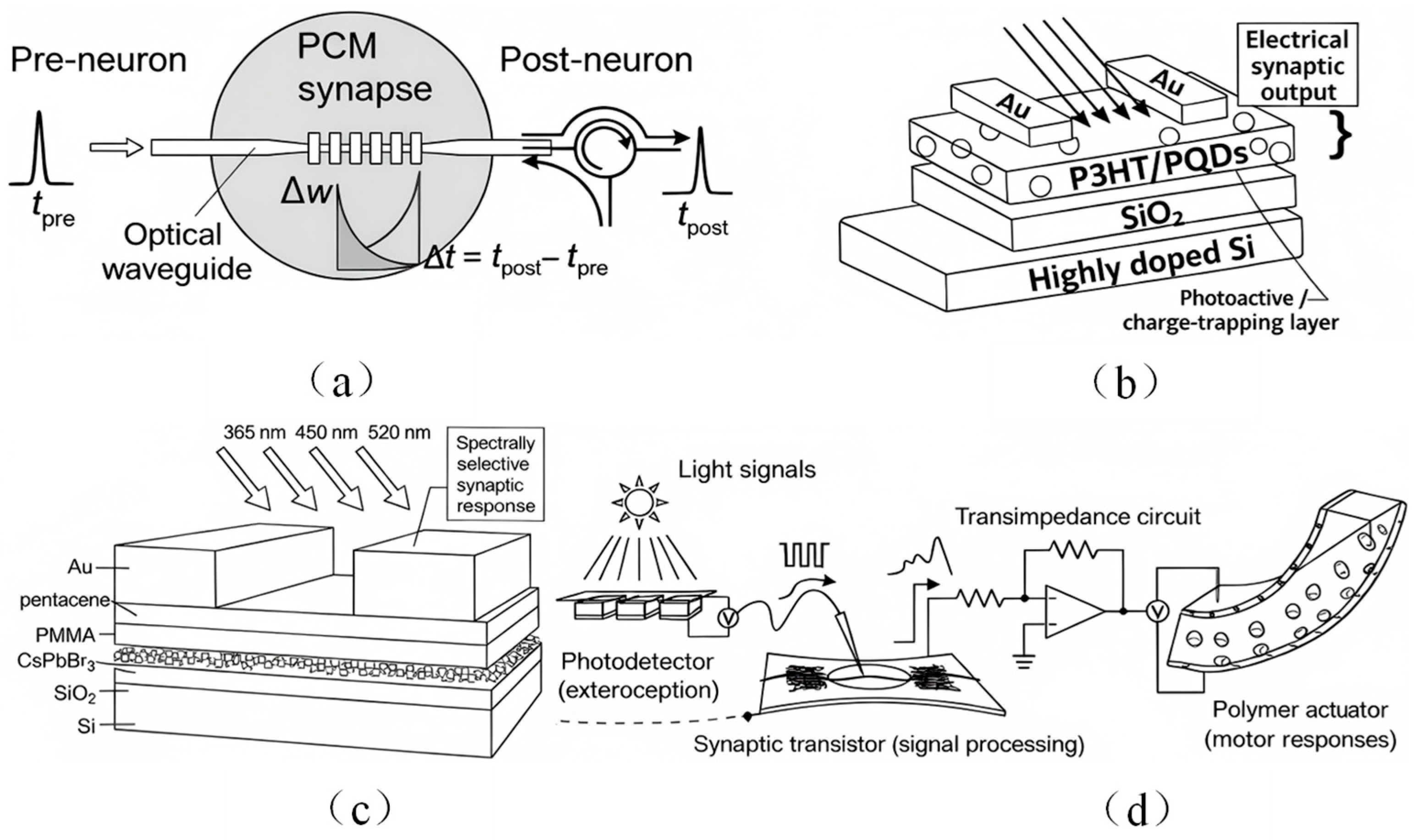
Taken together, these representative studies indicate that photonic synaptic devices have gradually evolved from single-device optical memory elements toward spectrally selective, array-level, and even biointegrated neuromorphic systems. Overall, current photonic synaptic devices can be broadly categorized into several representative routes, including pure photonic synapses, optoelectronic non-volatile memories, broadband and spectrally selective optoelectronic synapses, neuromorphic vision systems, and biointegrated optoelectronic sensorimotor systems. Figure 4 schematically summarizes the representative architectures of these categories.
Figure 4.
Representative architectures of photonic synaptic devices. (a) All-optical synapse based on waveguide-integrated phase-change modulation. (b) Optoelectronic non-volatile synapse based on light absorption, charge storage, and conductance modulation. (c) Broadband/spectrally selective optoelectronic synapse. (d) Integrated neuromorphic sensory–motor system for bioinspired optoelectronic processing.
As summarized in Table 2, representative photonic synaptic device categories differ in their core mechanisms, spectral response characteristics, integration level, and application scenarios, highlighting the trade-offs between bandwidth, energy efficiency, scalability, and system complexity.
Table 2.
Summary and critical comparison of representative photonic synaptic device categories.
2.3. Other Synaptic Devices
Beyond visual and tactile perceptions, biological systems interact with complex environments through diverse sensory modalities, including olfaction, audition, and magnetoreception. Emulating these diverse sensory capabilities has driven the development of various specialized artificial synaptic devices. Some scholars have conducted relevant research on the application of synaptic devices in humidity, temperature, sound, and magnetic fields.
Synaptic plasticity is defined as the ability of synapses to increase or decrease over time, and it is an important neurochemical basis for cognitive abilities. When designing artificial neural synapses, it is important to focus on building biomimetic synapses that can simulate basic synaptic plasticity in response to environmental factors. Guo et al. prepared an indium–tin–oxide synaptic transistor using proton-conducting nanogranular phosphorosilicate glass as the gate dielectric [34]. The gate senses environmental humidity and can regulate transistor current, simulating synaptic plasticity. This synaptic plasticity can serve as synaptic weights, providing device foundation for implementation in artificial neural morphological systems. Meanwhile, the device can be prepared at room temperature and has the potential for large-scale manufacturing. Similarly focusing on moisture sensing, Nie et al. constructed an artificial synaptic transistor based on indium–zinc-oxide (IZO) with a graphene oxide/chitosan composite electrolyte film as the gate dielectric [35]. This transistor can also be prepared at room temperature and effectively simulates synaptic plasticity. In order to quantitatively evaluate its performance, the excitatory post-synaptic current, paired-pulse facilitation index, and high-pass filtering coefficient were used for evaluation. Experiments have shown that the synaptic transistor has a higher humidity sensitivity, shorter response/recovery time (30 ms), and lower energy consumption (2.2 nJ), which balances its various performance parameters in the neuromorphic system well. While these proton-gated oxide transistors successfully emulate humidity-dependent plasticity with low energy consumption and room temperature processing, their long-term stability and precise control in highly fluctuating ambient environments remain critical challenges for practical deployment.
Although MoS2 has been applied in many artificial neural synapse devices, it is mainly limited to pressure sensing or photodetecting systems. Expanding the sensory scope, Sun et al. proposed a synaptic computation based on Joule heating and a versatile doping-induced metal-insulator transition in scalable monolayer-MoS2 [36]. The tunable synaptic plasticity is realized through Joule heating of the device channel, which integrates STP into a single device. This synaptic device has sound intensity suppression and frequency dependence, so it can detect the time difference between reaching synapses and achieving sound localization. In terms of power consumption, single-device synaptic events only consume about 10 fJ, which is equivalent to actual biological behavior. This achievement demonstrates for the first time the application in the field of sound and expands the research direction of artificial neural synapses. By integrating Joule heating and structural-phase transitions in 2D materials, this auditory synapse achieves biological-level energy efficiency for sound localization. However, precisely controlling the local thermal dynamics and scaling such thermo-sensitive devices in dense integrated arrays require further thermal management engineering.
In nature, certain animals possess magnetocognitive abilities for navigation and orientation. Inspired by this, Kim et al. designed an air-suspended magneto-interactive top-gate structure based on a ferroelectric field-effect transistor [37]. According to the changes in the magnetic field, the suspended gate formed by laminating superparamagnetic particles and conductive polymers will undergo deformation. The contact area between the gate and the underlying ferroelectric layer is thereby changed, which achieves a modulation of channel conductivity. Experimental results have shown that the conductivity modulation can be quantified as a function of the magnetic pulse amplitude, quantity, and time interval. This device first realizes the application of artificial neural synapses in magnetic fields and can serve as the basic device for an artificial intelligence synaptic compass. This biomimetic approach elegantly expands the sensory spectrum to magnetic fields, establishing a foundation for artificial compasses. Nevertheless, the reliance on complex air-suspended micromechanical structures and elastomeric composites introduces significant fabrication complexity and potential mechanical fatigue issues under prolonged operation.
Overall, the continuous expansion of artificial synapses into humidity, auditory, and magnetic sensory domains demonstrates the massive potential for constructing omni-sensory neuromorphic platforms. These emerging devices break the boundaries of traditional computing hardware, offering specialized pathways for environmental monitoring, sound localization, and self-navigation. A summary and critical comparison of these representative “other” synaptic device categories is provided in Table 3.
Table 3.
Summary and critical comparison of other emerging synaptic device categories.
3. Challenges
Although synaptic devices have received sufficient attention from the academic community in recent years and have made significant progress, the research content is relatively divergent and has not formed a mainstream roadmap. At the application level, there are also many issues in terms of materials, functionality, and morphology.
Firstly, artificial electronic skin is one of the important application areas for synaptic devices. At present, most synaptic devices are still implemented using traditional semiconductor device architectures, which cannot withstand sufficient mechanical stress and bending application requirements (e.g., rigid inorganic semiconductors like silicon easily fracture under tensile strains of approximately 1% [38]). Therefore, they cannot simulate human skin realistically, which limits their applications in intelligent robots and medical health. Based on organic thin films, two-dimensional (2D) materials, and one-dimensional materials, some scholars have attempted to design device architectures and have made certain progress. However, the differences between flexible electronic devices and traditional semiconductor materials require a further exploration of their conductivity and control mechanisms in order to integrate them with mainstream artificial neural network algorithms and achieve efficient signal processing and computation.
Secondly, existing synaptic devices often can only achieve certain types of functions, such as pressure and light perception. However, the perception of natural physical quantities such as temperature, humidity, sound, gas, and magnetic field in the application of artificial skin is still in its initial stage. Therefore, exploring new materials and device architectures, and being able to carry corresponding neural network algorithms forward to meet the various needs of signal perception and computing, is a new frontier that synaptic devices urgently need to explore.
Thirdly, the reported synaptic devices are typically only capable of sensing a single physical quantity and are concentrated in the fields of pressure and optical signals. A few research achievements have developed some dual-mode synaptic devices that can process both signals simultaneously. But, for intelligent robots and edge computing applications, the same device or system needs to imitate human skin and simultaneously perceive multiple types of natural signals at the same time. However, the semiconductor thin films currently used in synaptic devices have a single function and cannot achieve multimodal functionality. As is well known, most organisms have multiple sensory organs that can simultaneously perceive various physical changes in their environment. Therefore, multisensory memory computing (MSMC) that can integrate and organize various sensory information is the foundation for effective perceptual and cognitive functions. Although multiple different sensory receptors and processing nodes can be used to generate multisensory raw data and process different sensory information separately, the subsequent data transmission and the increase in the number of perception units slow down the overall work speed. The separation of perception units and processing nodes also leads to differences in transmission speed, which will further limit conversion speed and increase energy consumption. Therefore, exploring the architecture of multi-sensing devices that integrate MSMC functionality is a necessary path for the future development of synaptic devices.
Fourthly, deploying artificial synapses in a large-scale Artificial Neural Network (ANN) faces critical challenges from hardware non-idealities. Unlike ideal software-based weights, practical synaptic devices frequently exhibit severe non-linearity and asymmetry during conductance tuning. When applying identical potentiation and depression pulses, the conductance change is often abrupt in one direction and saturated in the other. This asymmetric weight update directly breaks gradient descent rules, severely degrading the learning accuracy of algorithms relying on backpropagation. Furthermore, cycle-to-cycle and device-to-device spatial–temporal variability introduces unpredictable noise into the synaptic crossbar arrays. Such hardware variability significantly hinders the reliable mapping of pre-trained offline weights onto the physical hardware, causing a catastrophic drop in inference accuracy when executing complex tasks like image classification or speech recognition [39].
4. Solutions
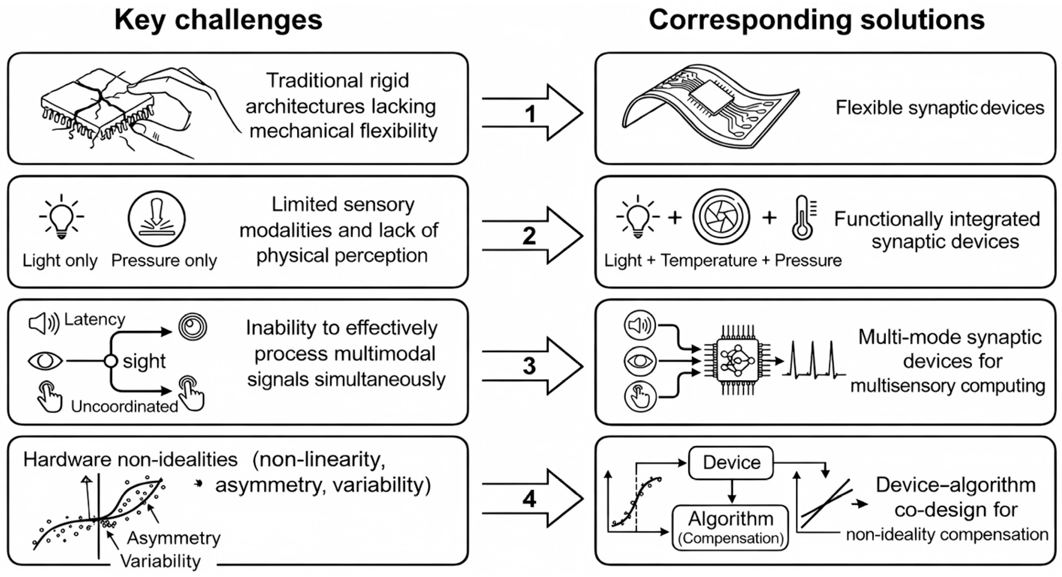
To systematically address the limitations and bottlenecks identified in Section 3, researchers have proposed targeted solutions at the material, functional, and system-architecture levels. These emerging solutions can be broadly organized into mechanically adaptive flexible devices, functionally integrated architectures, multimodal sensory–memory–computing systems, and hardware-aware algorithm co-design strategies. This section highlights these emerging pathways. To provide a clearer overview of the challenge–solution relationships discussed in this section, the major challenges and their corresponding solution pathways are schematically summarized in Figure 5.
Figure 5.
Challenge–solution linkage for neuromorphic sensory–computing systems.
As shown in Figure 5, current efforts to advance artificial synaptic devices are mainly focused on improving mechanical adaptability, expanding perceptual dimensionality, enabling efficient multimodal information processing, and compensating for hardware non-idealities through system-level co-design.
4.1. Flexible Synaptic Devices
To address the limitation that traditional rigid semiconductor architectures cannot withstand sufficient mechanical stress (as discussed in Section 3), flexible synaptic devices have been extensively developed. Combined with Au electrodes, poly (3-hydroxylthiophene, P3HT) active channels, and ion-conducting membranes, Fu et al. proposed a highly interconnected neuromorphic architecture (HINA) based on flexible self-supported multi-terminal organic transistors [40]. In this organic neuromorphic device, free-standing ion-conducting membranes are adopted as gate dielectric and substrate. Unlike other artificial neurons that only have multi-inputs to one output or one input to multi-outputs, HINA realizes multi-inputs and multi-outputs. Furthermore, there is a high degree of correlation between various input and output signals, which can perform complicated learning and memory functions. The prepared neural morphological device still exhibits excellent electrical stability and mechanical flexibility after 1000 bends. A 3 × 3 post-neuron array was constructed to mimic the neural architecture of the human brain. According to Pavlov’s learning rule, the dynamic processes of memory and forgetting were realized.
In the human or animal body, the skin and organs are very soft and can adapt to various forms of deformation. Even if the neural synapses in the skin undergo deformation, they can still maintain sensitive responses to external stimuli. Therefore, in recent years, soft artificial synapses have also made significant progress. Shim et al. developed a stretchable synaptic transistor based on elastic electronic materials, which can maintain its original device performance even when stretched to 50% [41]. Based on this device, an arrayed artificial skin was constructed with patterned gate electrodes, pressure-sensitive rubber, gate electrodes of the rubbery synaptic transistor array, and polydimethylsiloxane (PDMS) encapsulation. Finally, a soft robot was entirely covered with this arrayed artificial skin. The robot was able to perform straight walking and turning in the directions left and right.
Oh et al. proposed a flexible artificial synapse utilizing the low-temperature deposition process (<150 °C) of silicon–indium–zinc-oxide (SIZO) and the flatness of a poly (4-vinylphenol) buffer layer. This flexible artificial synapse utilizes ion movement in ion gel to adjust the conductivity value (G) of the conductive channel, exhibiting excellent electrical properties that enable it to quickly respond to external signal stimuli [42]. It also exhibits extremely stable synaptic performance under high mechanical (bending) conditions and can still maintain device functionality after 1500 bending experiments. When different voltage values are applied, the postsynaptic conductivity of the device produces different response values, making it a good hardware carrier for neural network algorithms. Because the flexible artificial synapse has a very large Gmax/Gmin (the minimum–maximum weight) range, it can provide precise modulation for neural network weights. A sensory–neuromorphic system for sign language translation for hearing-impaired people was presented. After 100 training epochs, the ANN was well trained for input hand signs. The accuracy of each sign was up to 99.4%. Furthermore, it can be extended and applied to other wearable sensory–neuromorphic systems.
With a LiSiOx solid-state electrolyte and semiconducting 2D-MoS2 channel, Hwang et al. introduced an ultraflexible artificial–synaptic array device for wearable electronic devices [43]. Without a transfer step, it was fabricated on a flexible glass substrate. Thus, the occurrence of defects during transfer can be avoided and the fabrication time can be shortened. Based on a 28 × 28 pixel array, a three-layer neural network structure was built. By applying the Modified National Institute of Standards and Technology (MNIST) dataset, the recognition accuracy was as high as 98%. Even when bent for more than 400 cycles with a diameter of 10 mm, the recognition accuracy was above 95%. Experiments have shown that the device can maintain good neuromorphic performance within 700 folds. Compared with other devices that use IZO, IWO, and IGZO, the flexible synaptic transistor only uses a 5 V power supply and has the characteristic of low power consumption, which can support long-term standby use. Meanwhile, the sample synthesis method adopted has the potential for neuromorphic synaptic devices with mass production. While these flexible devices significantly improve mechanical adaptability for artificial skin, achieving long-term environmental reliability, large-area uniform fabrication, and seamless compatibility with dense ANN arrays remains an ongoing challenge.
4.2. Functionally Integrated Synaptic Devices
To break through the limitations of single-sensory capabilities and expand the perceptive spectrum of artificial skins (as discussed in Section 3), functionally integrated synaptic devices have been extensively explored. Unlike multimodal devices that process diverse physical stimuli (discussed in Section 4.3), this approach focuses on integrating the entire functional chain—sensing, transmission, memory, computing, and adaptation—within a single unified architecture. The human nervous system has various abilities such as perception, transmission, memory, and adaptation. In order to achieve these functions, Tan et al. proposed a photoelectronic pulse input neural system with perception, neural encoding, perception learning, and memory capabilities [44]. First, the external signal is converted into optical pulses and input into optoelectric synapses (OE synapses). The OE synapse was manufactured based on ITO/ZnO/NSTO materials. This non-contact signal transmission reduces the noise and crosstalk generated by system connections, achieving high-quality optical communication between distributed receptors and synaptic photoresistors. The OE synapse can simultaneously process multiple inputs, which provides the emulation of multiple action potentials from various axon terminals of pre-neurons to dendrites of post-neurons. By implementing the two main biological neural encoding principles of frequency and time encoding, the OE synapse can not only detect and distinguish different inputs, but also recognize Morse code, braille characters, and object motion. Combined with neural network algorithms, this device can also achieve feature extraction (encoding) and learning, thereby recognizing and memorizing handwritten letters and words.
Previous artificial tactile perception systems only had two functions: sensing and computing. However, in practical applications, information storage can effectively improve computational efficiency. Xie et al. built an artificial tactile perception system based on a silk fiber (SF) composite memristor and an AgNWs/PDMS pressure sensor [45]. The SF composite memristor has the characteristics of low switching voltage, extended holding time, and stable durability, and has achieved complete synaptic functions. At the same time, the device also has good response speed and durability to stimulation signals. The SF composite memristor converts the received pressure stimulus into current, while integrating sensing, storage, and computing functions.
By vertically integrating synaptic transistors with graphene oxide channels, an ionogel gate dielectric, and an elastomeric fingerprint-like receptive layer, Hong et al. introduced an array of artificial synaptic mechanoreceptors (ASMRs) with built-in synaptic functions [46]. The array has eight slowly adapting (SA) and eight fast-adapting (FA) mechanoreceptors, which first realize the response to prolonged pressure, vibration, and impact. First, the triboelectric–capacitive gate located between the receptive layer and the gate dielectric responds to external tactile stimuli and generates induced currents. This array integrates machine learning algorithms to achieve the real-time perception and computation of tactile signals. Ultimately, integrating ASMR into bio-inspired intelligent skin can achieve the functionality of recognizing handwriting styles, surface patterns, and textures. The experimental results show that ASMR has both compactness and extremely high perception accuracy and has a high application value in edge AI scenarios such as neuro-robotics, autonomous systems, and intelligent healthcare. Overall, functionally integrated devices successfully move beyond simple stimulus–response emulation to system-level processing. However, balancing ultra-compactness, stable multifunctionality, and low-power operation within a single footprint remains difficult.
4.3. Multi-Mode Synaptic Devices
To resolve the severe latency and energy overhead caused by physically separated sensor nodes (as discussed in Section 3), cutting-edge research has shifted toward multisensory memory computing (MSMC) architectures. Building upon the functional integration in Section 4.2, MSMC emphasizes the synergistic perception and computation of diverse physical inputs (e.g., visual, tactile, thermal) simultaneously. Artificial intelligence skin needs to have both sensing and memory capabilities for temperature and deformation, which is of great significance for monitoring physiological changes in the human body and preventing diseases. Wang et al. first developed an intrinsic stretchable neural morphology transistor with mechanical and thermal sensors [47]. Based on the array composed of this transistor, the team further developed a stretchable temperature responsive multimodal neuromorphic electronic skin (STRM-NES) with sensing and memory functions. The synaptic plasticity of this smart skin can be regulated through multiple modalities, in situ temperature changes, and tensile deformation, and has a temperature-responsive function, spontaneous recovery, and temperature-dependent autonomous learning ability. STRM-NES exhibits multimodal performance in perception, transmission, memory, and recovery from external stimuli.
In order to simulate the perception ability of human skin to external stimuli more realistically, Wan et al. proposed a bimodal artificial sensory neuron (BASE), which mainly includes a resistive pressure sensor, a perovskite-based photodetector, a hydrogel-based ionic cable, and a synaptic transistor [48]. The pressure sensors and photodetectors respectively sense tactile and visual signals and convert them into electrical signals. Afterwards, the electrical signal is transmitted to the synaptic transistor through the ionic cable and is finally integrated and converted into a post-transient current. By synchronizing the two signals to determine multidimensional spatial information, BASE can accurately control a robot hand. The research team also designed and simulated a matrix of BASE as the feature extraction layer of a perceptron for the recognition of multi-transparency alphabetic patterns, which confirmed that the fusion of bimodal sensation can improve the recognition rate.
Fu et al. designed a bionic visual–audio photodetector (VAPD) based on a vertically stacked graphene–germanium (Gra-Ge) hybrid field-effect phototransistor [49]. As an artificial neural synapse, this detector effectively integrates visual and auditory perception abilities, enabling single unit “viewing” and “listening”. By adjusting the photoresponsive voltage of the gate, synaptic weights can be programmed to achieve visual feature extraction, object classification, and acoustic manipulation. At the same time, the device also has excellent responsiveness and response speed, which provides a new development direction for dual-mode or even multi-mode artificial neural synapses. Although these multimodal devices dramatically improve perceptual richness and biomimetic realism, managing complex signal coupling, structural hardware complexity, and synchronized multi-channel information processing still limits their large-scale scalability.
4.4. Device–Algorithm Co-Design for Hardware Compensation
To mitigate the severe performance degradation caused by hardware non-idealities such as non-linearity, asymmetry, and variability (Challenge 4), device–algorithm co-design has emerged as a crucial system-level solution [50]. Rather than solely relying on material engineering to pursue perfectly ideal synapses, researchers are increasingly developing hardware-aware training algorithms that incorporate these physical non-idealities directly into the software training loop [51]. By pre-training the ANN with actual physical noise models and asymmetric conductance updates, the algorithm can autonomously adapt to the hardware’s intrinsic defects, thereby compensating for the accuracy loss. Additionally, hybrid precision computing architectures provide a practical pathway where highly precise digital processors handle critical gradient error calculations, while analog synaptic arrays perform the heavy, error-tolerant matrix–vector multiplications. This synergistic co-design effectively bridges the gap between imperfect physical devices and high-precision algorithm requirements. Although this co-design paradigm significantly alleviates the impact of hardware non-idealities, it inherently increases overall system complexity and demands a much tighter interdisciplinary coordination among physical hardware characterization, integrated circuit design, and software learning algorithms.
5. Conclusions and Future Perspectives
Although the roadmaps of different synaptic devices have their own characteristics, they are gradually moving from laboratory concept validation to system-level implementation with greater engineering potential. But the essence of synaptic devices lies not only in the outstanding performance of single-sensory modalities, but also in the efficient fusion and collaboration of multimodal information. Therefore, the future of integrated sensing and computing will inevitably evolve from single-modal deepening to multimodal fusion and device–algorithm co-design.
However, artificial synaptic devices are not simply a combination of single-sensory functions, but stem from the deep fusion and collaborative interpretation of multisensory information in the artificial nervous system. Thereby, it can generate scene understanding that goes beyond single-sensory perception. Despite the vast prospects, the road to multimodal computing integration still presents numerous challenges. The primary obstacle is the significant differences in physical basis, signal characteristics, and spectral ranges of different perception modes, which poses a severe challenge to the heterogeneous integration of materials science and chip technology. Secondly, the synchronization challenges of different modal data in terms of generation speed, data format, and spatiotemporal aspects make cross-modal interaction extremely challenging. Furthermore, the existing algorithm models cannot fully unleash the potential of multimodal systems. Tailoring hardware-aware algorithms through device–algorithm co-design will be crucial to take these systems to the next level.
In the future, intelligent terminals and robots may have integrated perception capabilities similar to those of humans, such as “seeing, understanding, smelling, and touching”. And artificial intelligence will no longer rely on cloud computing support, truly achieving an evolutionary model of autonomous growth and continuous learning in the physical world. Continued advances in synaptic devices will play a key role in the future development of integrated sensing and computing systems.
Author Contributions
Conceptualization, Z.C. and Y.H.; software simulation and parameter optimization, Z.C.; data processing, Z.C.; writing—original draft preparation, Z.C.; writing—review and editing, Z.C., C.C. and Y.H.; supervision, C.C. and Y.H. All authors have read and agreed to the published version of the manuscript.
Funding
National Natural Science Foundation of China (6247011759).
Data Availability Statement
The original contributions presented in this study are included in the article. Further inquiries can be directed to the corresponding author.
Conflicts of Interest
The authors declare no conflicts of interest. The funders had no role in the design of the study; in the collection, analyses, or interpretation of data; in the writing of the manuscript; or in the decision to publish the results.
References
- Zhu, L.Q.; Wan, C.J.; Guo, L.Q.; Shi, Y.; Wan, Q. Artificial synapse network on inorganic proton conductor for neuromorphic systems. Nat. Commun. 2014, 5, 3158. [Google Scholar] [CrossRef] [Scilit]
- Li, Y.; Zhong, Y.; Zhang, J.; Xu, L.; Wang, Q.; Sun, H.; Tong, H.; Cheng, X.; Miao, X. Activity-dependent synaptic plasticity of a chalcogenide electronic synapse for neuromorphic systems. Sci. Rep. 2014, 4, 4906. [Google Scholar] [CrossRef] [Scilit]
- Zhang, C.; Tai, Y.T.; Shang, J.; Liu, G.; Wang, K.L.; Hsu, C.; Yi, X.; Yang, X.; Xue, W.; Tan, H.; et al. Synaptic plasticity and learning behaviours in flexible artificial synapse based on polymer/viologen system. J. Mater. Chem. C 2016, 4, 3217–3223. [Google Scholar] [CrossRef] [Scilit]
- Zang, Y.; Shen, H.; Huang, D.; Di, C.A.; Zhu, D. A dual-organic-transistor-based tactile perception system with signal-processing functionality. Adv. Mater. 2017, 29, 1606088. [Google Scholar] [CrossRef] [Scilit]
- Taube, N.W.; Garcia, N.C.; Shakthivel, D.; Vinciguerra, V.; Labeau, F.; Gregory, D.H.; Dahiya, R. Nanowire FET based neural element for robotic tactile sensing skin. Front. Neurosci. 2017, 11, 501. [Google Scholar]
- John, R.A.; Ko, J.; Kulkarni, M.R.; Tiwari, N.; Chien, N.A.; Ing, N.G.; Leong, W.L.; Mathews, N. Flexible ionic-electronic hybrid oxide synaptic TFTs with programmable dynamic plasticity for brain-inspired neuromorphic computing. Small 2017, 13, 1701193. [Google Scholar] [CrossRef] [Scilit] [PubMed]
- Gerasimov, J.Y.; Gabrielsson, R.; Forchheimer, R.; Stavrinidou, E.; Simon, D.T.; Berggren, M.; Fabiano, S. An evolvable organic electrochemical transistor for neuromorphic applications. Adv. Sci. 2019, 6, 1801339. [Google Scholar] [CrossRef] [Scilit] [PubMed]
- Kim, D.W.; Yang, J.C.; Lee, S.K.; Park, S. Neuromorphic processing of pressure signal using integrated sensor-synaptic device capable of selective and reversible short- and long-term plasticity operation. ACS Appl. Mater. Interfaces 2020, 12, 23207–23216. [Google Scholar] [CrossRef] [Scilit]
- Kim, Y.; Chortos, A.; Xu, W.T.; Liu, Y.X.; Oh, J.Y.; Son, D.H.; Kang, J.H.; Foudeh, A.M.; Zhu, C.X.; Lee, Y.J.; et al. A bioinspired flexible organic artificial afferent nerve. Science 2018, 360, 998–1003. [Google Scholar] [CrossRef] [Scilit]
- Wan, C.J.; Chen, G.; Fu, Y.M.; Wang, M.; Matsuhisa, N.; Pan, S.W.; Pan, L.; Yang, H.; Wan, Q.; Zhu, L.Q.; et al. An artificial sensory neuron with tactile perceptual learning. Adv. Mater. 2018, 30, 1801291. [Google Scholar] [CrossRef] [Scilit]
- Ham, S.; Kang, M.; Jang, S.; Jang, J.; Wang, G. One-dimensional organic artificial multi-synapses enabling electronic textile neural network for wearable neuromorphic applications. Sci. Adv. 2020, 6, eaba1178. [Google Scholar] [CrossRef] [Scilit]
- Lee, Y.R.; Trung, T.Q.; Hwang, B.U.; Lee, N.E. A flexible artificial intrinsic-synaptic tactile sensory organ. Nat. Commun. 2020, 11, 2753. [Google Scholar] [CrossRef] [Scilit]
- Kim, W.J.; Lee, K.H.; Choi, S.Y.; Park, E.; Kim, G.; Ha, J.B.; Kim, Y.; Jang, J.H.; Oh, J.H.; Kim, H.Y.; et al. Electrochemiluminescent tactile visual synapse enabling in situ health monitoring. Nat. Mater. 2025, 24, 925–934. [Google Scholar] [CrossRef] [Scilit] [PubMed]
- Xu, F.; Xu, J.; Zhang, X.; Wei, M.; Yu, H.; Chai, J.; Song, X.; Qin, Y.; Wang, F. Metal oxide nanowire synaptic transistor for self-powered visual tactile human–machine interaction system. IEEE Trans. Electron Devices 2026, 73, 2176–2184. [Google Scholar] [CrossRef] [Scilit]
- Wright, C.D.; Liu, Y.; Kohary, K.I.; Aziz, M.M.; Hicken, R.J. Arithmetic and biologically inspired computing using phase-change materials. Adv. Mater. 2011, 23, 3408–3413. [Google Scholar] [CrossRef] [Scilit] [PubMed]
- Kuzum, D.; Jeyasingh, R.G.D.; Lee, B.; Wong, H.-S.P. Nanoelectronic programmable synapses based on phase-change materials for brain-inspired computing. Nano Lett. 2012, 12, 2179–2186. [Google Scholar] [CrossRef] [Scilit] [PubMed]
- Tuma, T.; Pantazi, A.; Gallo, M.L.; Sebastian, A.; Eleftheriou, E. Stochastic phase-change neurons. Nat. Nanotechnol. 2016, 11, 693–699. [Google Scholar] [CrossRef] [Scilit]
- Wong, H.-S.P.; Lee, H.-Y.; Yu, S.; Chen, Y.-S.; Wu, Y.; Chen, P.-S.; Lee, B.; Chen, F.T.; Tsai, M.J. Metal–oxide RRAM. Proc. IEEE 2012, 100, 1951–1970. [Google Scholar] [CrossRef] [Scilit]
- Jo, S.H.; Chang, T.; Ebong, I.; Bhadviya, B.B.; Mazumder, P.; Lu, W. Nanoscale memristor device as synapse in neuromorphic systems. Nano Lett. 2010, 10, 1297–1301. [Google Scholar] [CrossRef] [Scilit]
- Chanthbouala, A.; Garcia, V.; Cherifi, R.O.; Bouzehouane, K.; Fusil, S.; Moya, X.; Xavier, S.; Yamada, H.; Deranlot, C.; Mathur, N.D.; et al. A ferroelectric memristor. Nat. Mater. 2012, 11, 860–865. [Google Scholar] [CrossRef] [Scilit]
- Alibart, F.; Pleutin, S.; Bichler, O.; Gamrat, C.; Serrano-Gotarredona, T.; Linares-Barranco, B.; Vuillaume, D. A memristive nanoparticle/organic hybrid synapstor for neuroinspired computing. Adv. Funct. Mater. 2012, 22, 609–616. [Google Scholar] [CrossRef] [Scilit]
- Chen, C.L.; Kim, K.; Truong, Q.; Shen, A.; Li, Z.; Chen, Y. A spiking neuron circuit based on a carbon nanotube transistor. Nanotechnology 2012, 23, 275202. [Google Scholar] [CrossRef] [Scilit]
- Cheng, Z.G.; Rios, C.; Pernice, W.H.P.; Wright, C.D.; Bhaskaran, H. On-chip photonic synapse. Sci. Adv. 2017, 3, e1700160. [Google Scholar] [CrossRef] [Scilit]
- Chen, J.Y.; Yang, D.L.; Jhuang, F.C.; Fang, Y.H.; Benas, J.S.; Liang, F.C.; Kuo, C.C. Ultrafast responsive and low-energy-consumption poly(3-hexylthiophene)/perovskite quantum dots composite film-based photonic synapse. Adv. Funct. Mater. 2021, 31, 2105911. [Google Scholar] [CrossRef] [Scilit]
- Wang, Y.; Lv, Z.Y.; Chen, J.R.; Wang, Z.P.; Zhou, Y.; Zhou, L.; Chen, X.L.; Han, S.T. Photonic synapses based on inorganic perovskite quantum dots for neuromorphic computing. Adv. Mater. 2018, 30, 1802883. [Google Scholar] [CrossRef] [Scilit] [PubMed]
- Seo, S.W.; Jo, S.H.; Kim, S.H.; Shim, J.W.; Oh, S.Y.; Kim, J.H.; Heo, K.; Choi, J.W.; Choi, C.H.; Oh, S.; et al. Artificial optic-neural synapse for colored and color-mixed pattern recognition. Nat. Commun. 2018, 9, 5106. [Google Scholar] [CrossRef] [Scilit] [PubMed]
- Yin, L.; Han, C.; Zhang, Q.T.; Ni, Z.; Zhao, S.Y.; Wang, K.; Li, D.S.; Xu, M.S.; Wu, H.Q.; Pi, X.D.; et al. Synaptic silicon-nanocrystal phototransistors for neuromorphic computing. Nano Energy 2019, 63, 103859. [Google Scholar] [CrossRef] [Scilit]
- Xin, S.; Wang, T.; Dou, K.; Zheng, L.; Wu, L.; Chen, Q.; Ji, S.; Ding, G.; Seeram, R.; Zhou, Y.; et al. Negative photoconductivity in nanowires/QDs heterojunction network for neuromorphic visual perception. Adv. Funct. Mater. 2025, 35, 2504250. [Google Scholar] [CrossRef] [Scilit]
- Park, H.L.; Kim, H.; Lim, D.Y.; Zhou, H.Y.; Kim, Y.H.; Lee, Y.J.; Park, S.J.; Lee, T.W. Retina-inspired carbon nitride-based photonic synapses for selective detection of UV light. Adv. Mater. 2020, 32, 1906899. [Google Scholar] [CrossRef] [Scilit]
- Zhou, F.C.; Zhou, Z.; Chen, J.W.; Choy, T.H.; Wang, J.L.; Zhang, N.; Lin, Z.Y.; Yu, S.M.; Kang, J.F.; Wong, H.-S.P.; et al. Optoelectronic resistive random access memory for neuromorphic vision sensors. Nat. Nanotechnol. 2019, 14, 776–782. [Google Scholar] [CrossRef] [Scilit]
- Mennel, L.; Symonowicz, J.; Wachter, S.; Polyushkin, D.K.; Molina-Mendoza, A.J.; Mueller, T. Ultrafast machine vision with 2D material neural network image sensors. Nature 2020, 579, 62–66. [Google Scholar] [CrossRef] [Scilit]
- Kwak, K.; An, J.B.; Lee, I.S.; Hwang, Y.S.; Son, H.J.; Kim, H.J. Toward monolithic 3D integration of in-sensor neuromorphic vision systems using metal-oxide semiconductors. Device 2025, 3, 100900. [Google Scholar] [CrossRef] [Scilit]
- Lee, H.; Jiang, Z.; Yokota, T.; Fukuda, K.; Park, S.; Someya, T. Stretchable organic optoelectronic devices: Design of materials, structures, and applications. Mater. Sci. Eng. R Rep. 2021, 146, 100631. [Google Scholar] [CrossRef] [Scilit]
- Guo, L.Q.; Wen, J.; Zhu, L.Q.; Ming, Y.; Xiao, H. Humidity dependent synaptic plasticity for proton-gated oxide synaptic transistor. IEEE Electron Device Lett. 2017, 38, 1248–1251. [Google Scholar] [CrossRef] [Scilit]
- Nie, S.; He, Y.L.; Liu, R.; Shi, Y.; Wan, Q. Low-voltage oxide-based synaptic transistors for spiking humidity detection. IEEE Electron Device Lett. 2019, 40, 459–462. [Google Scholar] [CrossRef]
- Sun, L.F.; Zhang, Y.S.; Hwang, G.W.; Jiang, J.B.; Kim, D.Y.; Eshete, Y.; Zhao, R.; Yang, H. Synaptic computation enabled by Joule heating of single-layered semiconductors for sound localization. Nano Lett. 2018, 18, 3229–3234. [Google Scholar] [CrossRef] [Scilit] [PubMed]
- Kim, Y.; Lee, K.; Lee, J.; Jang, S.; Kim, H.; Lee, H.; Lee, S.; Wang, G.; Park, C. Bird-inspired self-navigating artificial synaptic compass. ACS Nano 2021, 15, 20116–20126. [Google Scholar] [CrossRef] [Scilit]
- Bo, R.; Xu, S.; Yang, Y.; Zhang, Y. Mechanically guided 3D assembly for architected flexible electronics. Chem. Rev. 2023, 123, 11137–11189. [Google Scholar] [CrossRef] [Scilit]
- Kim, K.; Song, M.S.; Hwang, H.; Hwang, S.; Kim, H. A comprehensive review of advanced trends: From artificial synapses to neuromorphic systems with consideration of non-ideal effects. Front. Neurosci. 2024, 18, 1279708. [Google Scholar] [CrossRef] [Scilit] [PubMed]
- Ying, F.; Kong, L.A.; Yang, C.; Wang, J.; Qian, C.; Yuan, Y.; Jia, S.; Gao, Y.; Wan, Q. Flexible neuromorphic architectures based on self-supported multi-terminal organic transistors. ACS Appl. Mater. Interfaces 2018, 10, 26443–26450. [Google Scholar]
- Shim, H.; Sim, K.; Ershad, F.; Yang, P.Y.; Thukral, A.; Rao, Z.; Kim, H.J.; Liu, Y.H.; Wang, X.; Gu, G.Y.; et al. Stretchable elastic synaptic transistors for neurologically integrated soft engineering systems. Sci. Adv. 2019, 5, eaax4961. [Google Scholar] [CrossRef] [Scilit]
- Oh, S.; Cho, J.L.; Lee, B.H.; Seo, S.; Lee, J.H.; Choo, H.; Heo, K.; Lee, S.Y.; Park, J.H. Flexible artificial Si-In-Zn-O/ion gel synapse and its application to sensory-neuromorphic system for sign language translation. Sci. Adv. 2021, 7, eabg9450. [Google Scholar] [CrossRef] [Scilit]
- Hwang, Y.; Park, B.; Hwang, S.; Choi, S.W.; Kim, H.S.; Kim, A.R.; Choi, J.W.; Yoon, J.; Kwon, J.D.; Kim, Y. A bioinspired ultraflexible artificial van der Waals 2D-MoS2 channel/LiSiOx solid electrolyte synapse arrays via laser-lift-off process for wearable adaptive neuromorphic computing. Small Methods 2023, 7, 2201719. [Google Scholar] [CrossRef] [Scilit]
- Tan, H.W.; Tao, Q.Z.; Pande, I.; Majumdar, S.; Liu, F.; Zhou, Y.F.; Persson, P.O.Å.; Rosen, J.; van Dijken, S. Tactile sensory coding and learning with bio-inspired optoelectronic spiking afferent nerves. Nat. Commun. 2020, 11, 1369. [Google Scholar] [CrossRef] [Scilit] [PubMed]
- Xie, Y.L.; Kundu, S.C.; Fan, S.; Zhang, Y.P. Memristor-based artificial tactile perception systems with integrated functions of sensing and storage. Sci. China Mater. 2024, 67, 3675–3683. [Google Scholar] [CrossRef] [Scilit]
- Hong, S.J.; Lee, Y.R.; Bag, A.; Kim, H.S.; Trung, T.Q.; Sultan, M.J.; Moon, D.B.; Lee, N.E. Bio-inspired artificial mechanoreceptors with built-in synaptic functions for intelligent tactile skin. Nat. Mater. 2025, 24, 1100–1108. [Google Scholar] [CrossRef] [Scilit]
- Wang, Y.R.; Liu, D.X.; Zhang, Y.M.; Fan, L.C.; Ren, Q.Q.; Ma, S.H.; Zhang, M. Stretchable temperature-responsive multimodal neuromorphic electronic skin with spontaneous synaptic plasticity recovery. ACS Nano 2022, 16, 8283–8293. [Google Scholar] [CrossRef] [Scilit] [PubMed]
- Wan, C.J.; Cai, P.Q.; Guo, X.T.; Wang, M.; Matsuhisa, N.; Yang, L.; Lv, Z.S.; Luo, Y.F.; Loh, X.J.; Chen, X.D. An artificial sensory neuron with visual-haptic fusion. Nat. Commun. 2020, 11, 4602. [Google Scholar] [CrossRef] [Scilit] [PubMed]
- Fu, J.T.; Nie, C.B.; Sun, F.Y.; Li, G.L.; Shi, H.F.; Wei, X.Z. Bionic visual-audio photodetectors with in-sensor perception and preprocessing. Sci. Adv. 2024, 10, eadk8199. [Google Scholar] [CrossRef] [Scilit]
- Rasch, M.J.; Mackin, C.; Le Gallo, M.; Chen, A.; Fasoli, A.; Odermatt, F.; Li, N.; Nandakumar, S.R.; Narayanan, P.; Tsai, H.; et al. Hardware-aware training for large-scale and diverse deep learning inference workloads using in-memory computing-based accelerators. Nat. Commun. 2023, 14, 5282. [Google Scholar] [CrossRef] [Scilit]
- Cakal, U.; Maryada, A.; Wu, C.; Ulusoy, I.; Muir, D.R. Gradient-descent hardware-aware training and deployment for mixed-signal neuromorphic processors. Neuromorphic Comput. Eng. 2024, 4, 014011. [Google Scholar] [CrossRef] [Scilit]

Disclaimer/Publisher’s Note: The statements, opinions and data contained in all publications are solely those of the individual author(s) and contributor(s) and not of MDPI and/or the editor(s). MDPI and/or the editor(s) disclaim responsibility for any injury to people or property resulting from any ideas, methods, instructions or products referred to in the content. |
© 2026 by the authors. Licensee MDPI, Basel, Switzerland. This article is an open access article distributed under the terms and conditions of the Creative Commons Attribution (CC BY) license.