


Abstract
Self-assembled artificial nanostructures, such as DNA origami, have attracted interest as templates for the placement of inorganic materials because their design enables the incorporation of binding sites for attaching nanocomponents with nanometer-scale precision. In this work, we introduce a lithographically defined window-array substrate as an addressable platform for dark-field spectroscopic studies of individual DNA-origami-templated metallic nanostructures. The pattern was designed using the Nanometer Pattern Generation System (NPGS) software and written by electron beam lithography (EBL) on a SiOx/Si substrate. The role of the EBL pattern is to provide spatially separated measurement sites that facilitate the localization, selection, and optical interrogation of single-particle and dimer configurations. Metallic nanostructures created by the DNA origami technique, with programmable placement of spherical gold nanoparticles (Au NPs), are used here. The nanostructures are rectangular, measuring 70 nm × 90 nm, with an Au NP attached at one corner or at two opposite corners. These seed NPs are later enlarged by controlled coalescence via electroless silver deposition. Localized surface plasmon resonance (LSPR) studies by dark-field microscopy (DFM) are presented as a proof-of-concept application for evaluating the scattering response of individual silver-metalized nanoparticles and dimers.
1. Introduction
Plasmonics is a promising technology that exploits the unique optical properties of noble-metal nanostructures to modify and manipulate light at the nanoscale [1]. Under appropriate conditions, metallic nanoparticles can support collective light-induced electronic oscillations known as localized surface plasmons (LSPs), giving rise to localized surface plasmon resonances (LSPRs) [2,3]. These resonances can confine electromagnetic fields to nanoscale volumes and are therefore relevant for applications such as sensing, photonic devices, and enhanced spectroscopy [4,5]. When two or more noble-metal nanoparticles are brought into close proximity, their individual plasmon modes can couple, producing spectral shifts and intense local fields at interparticle gaps, commonly referred to as hot spots [6,7].
The fabrication of plasmonic nanostructures is commonly approached through either top-down lithography or bottom-up self-assembly. Electron beam lithography (EBL) offers high spatial resolution and direct patterning on solid substrates, but fabricating three-dimensional spherical nanoparticle assemblies with nanoscale gaps remains challenging [8]. Bottom-up methods, particularly DNA-based self-assembly, provide a complementary route because DNA can act as a programmable material for arranging inorganic components with nanometer precision [9,10,11,12,13,14,15,16,17]. In DNA origami, specific staple strands can be extended with binding sequences to attach DNA-functionalized nanoparticles at selected positions on a designed template [14,17].
DNA-origami-templated plasmonic structures are especially attractive because spherical gold nanoparticles can be positioned at predefined sites, functionalization, and subsequently enlarged by electroless metal deposition, metallization [18]. This enables the preparation of metallic single-particle and dimer configurations with designed nanoscale separations. Spherical nanoparticles are also convenient model systems for comparison with classical Mie-type plasmonic behavior [19]. Nevertheless, after synthesis of the gold nanoparticle–DNA origami hybrid nanostructures and silver metallization, a practical experimental challenge remains: the resulting nanostructures must be transferred to a solid substrate, spatially localized, identified, and optically interrogated without ambiguity from nearby particles, aggregates, or contaminants.
Dark-field microscopy and spectroscopy provide a suitable far-field approach for this purpose because individual metallic nanoparticles can be detected as bright scattering objects against a dark background [20,21,22]. However, random deposition on an unpatterned substrate can make single-particle analysis inefficient, since isolated particles, dimers, aggregates, and empty regions coexist without spatial registration. This complicates the correlation between morphology and optical response, particularly when the objective is to measure selected individual nanostructures.
After silver growth, the DNA-origami-templated metallic structures were transferred to a lithographically patterned SiOx/Si substrate for optical characterization. In this work, electron beam lithography was used to define a registered array of addressable measurement sites. Rectangular windows ~100 nm × 120 nm were patterned with a 5 μm center-to-center separation, allowing individual sites to be located by SEM and subsequently interrogated by dark-field microscopy. The purpose of this pattern is to simplify the identification of isolated target structures, reduce ambiguity caused by randomly distributed particles, aggregates, or contaminants, and enable correlation between electron microscopy inspection and optical readout.
The DNA origami structures used here consist of rectangular templates ~70 nm × 90 nm in size, functionalized with either one 5 nm Au NP at one corner or two 5 nm Au NPs at opposite corners. These seed NPs are enlarged to ~80 nm by electroless silver deposition. The resulting silver-metalized structures provide two model plasmonic configurations: an isolated nanoparticle and a nanoparticle dimer. The comparison between these configurations is used as a proof-of-concept demonstration of the proposed lithographic-window methodology for single-nanostructure plasmonic studies.
2. Materials and Methods
2.1. Synthesis
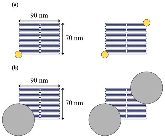
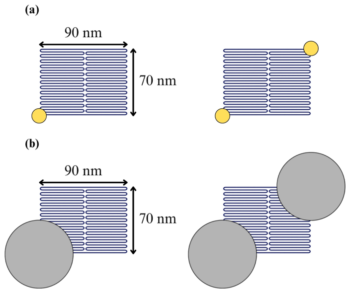
The idea behind DNA origami is to fold a DNA strand into an arbitrary 2D nanostructure [23]. The DNA strand used as a scaffold in the DNA origami technique is the single-stranded M13mp18 viral genome, which has 7249 bases. The DNA nanostructure chosen in this case is rectangular, measuring 70 nm × 90 nm, and has been reported elsewhere [18]. The design of this nanostructure is tailored by raster-filling the shape by folding the scaffold and properly choosing 225 short single strands, or staples, complementary to the scaffold to hold it in place. The staple strands can be further functionalized with various nanomaterials, making the origami a programmable breadboard for the location of anticipated nanoscale objects. A metallic nanostructure for plasmonic studies was fabricated by precisely placing commercially available spherical gold nanoparticles (Au NPs), 5 nm in size, at one corner or at each of two opposite corners of a rectangular origami via DNA hybridization, as shown in Figure 1a. This was possible by extending two neighboring staples to any corner of the rectangle, which act as binding sites because the sticky ends from each staple in the origami can bind complementary DNA-functionalized Au NPs [24].
Figure 1.
(a) Schematics showing the rectangular DNA nanostructure functionalized either with one AuNP at one corner or two AuNPs at opposite corners before the metallization process. (b) Schematics showing the functionalized rectangular DNA nanostructure shown in (a) after being metalized in a silver solution.
Afterward, the Au NPs bound to the DNA origami platform were enlarged in a controlled manner via electroless silver deposition, a method known as metallization [25]. By this means, the Au NPs serve as nucleation centers, with silver ions in solution coalescing around their surfaces as the metallization time is varied. A process for producing metallic nanostructures with a programmable design based on the specific positioning of Au NPs using the DNA origami technique and subsequent metallization has already been reported in detail [18]. Almost the same protocol was utilized here. In this work, the Au NPs attached to the DNA assemblies were grown to ~80 nm after 19 min of silver metallization, as shown schematically in Figure 1b.
2.2. Electron Beam Lithography
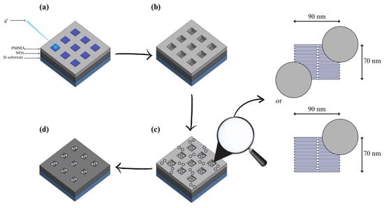
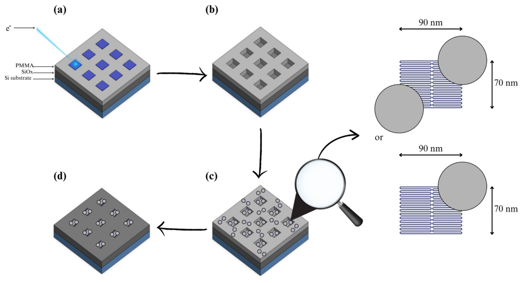
The synthesized metallic nanostructures, consisting of either one or two spherical silver-metalized NPs (~80 nm), kept in a buffer solution, require proper support for further experiments. A pattern engraved on a SiOx/Si surface by Electron Beam Lithography (EBL) was used here as a lithographically registered platform for isolating and optically addressing selected nanostructures by Dark-Field Microscopy (DFM). For this work, a pattern on a SiOx/Si surface was created as an array of rectangular apertures, or windows, separated by 5 μm. The windows were designed as addressable measurement sites. Based on scanning electron microscopes (SEMs), this technique writes a desired pattern in four basic steps: a beam of electrons is scanned across a surface covered with a resist film sensitive to the electrons, PMMA in this case, on the SiOx/Si substrate, as shown in Figure 2a. The electrons modify the polymer network in the desired pattern of the resist film, and later the pattern is visible after developing the resist from the surface, as shown in Figure 2b. Next, the metallic nanostructures based on DNA are deposited on the substrate after development, as shown in Figure 2c. The unexposed region of the resist can also be removed using a strong solvent to isolate specific nanostructures associated with the lithographic windows. This process is called lift-off in the EBL technique, see Figure 2d.
Figure 2.
Schematic representation of the EBL process used to define rectangular lithographic windows for the localization of DNA-origami-templated metallic nanostructures. (a) Electron beam exposure of a PMMA resist layer deposited on a SiOx/Si substrate to define the pattern. (b) Development of the exposed resist to produce rectangular lithographic windows. (c) Deposition and localization of DNA-origami-templated metallic nanostructures within each lithographic window. The subfigures in the top-right and bottom-right corners represent the occupation of a window by either a nanostructure with a dimer or a single metalized NP, respectively. (d) Lift-off process, leaving localized metallic nanostructures associated only with lithographic windows without resist. The orientations shown in (c,d) are illustrative; the rectangular windows may favor long-axis alignment but do not impose a unique in-plane orientation of the origami or the attached nanoparticles.
The endurance of DNA origami structures to the strong solvent acetone during the lift-off step was verified before running the EBL pattern. The details of the EBL procedure and results of endurance testing of the DNA origami nanostructures are given in the Appendix A. Prior to the actual EBL process, a pattern must be created and drafted on a computer, and the resulting file is then read by a program that serves as an interface between the drawing and the EBL system. In this work, the patterns were designed using the commercially available NPGS (Nanometer Pattern Generation System), which is intended to delineate complex structures from the nanometer to the micron scale using a commercial and conventional SEM [26].
There are three basic steps to generate a pattern: pattern design, parameter run file creation, and pattern writing. Firstly, the patterns are created using a CAD program. In this case, a square pattern (100 μm × 100 μm) was formed by an array of rectangular windows, nominally 100 nm × 120 nm and 5 μm, from center to center. The goal of this pattern is to define spatially separated and addressable measurement sites that increase the probability of finding isolated nanostructures suitable for single-object dark-field spectroscopy. The process does not impose deterministic filling of every window or a unique orientational alignment; rather, it provides a registered array of candidate measurement sites from which suitable single-particle or dimer configurations can be selected. The rectangular geometry of the EBL-defined windows was chosen to provide spatial registration sites with an aspect ratio comparable to that of the DNA origami template. This geometry may favor alignment of the origami’s long axis with the lithographic window’s long axis; however, the process does not impose a unique in-plane polarity or diagonal orientation. Therefore, the configurations shown schematically in Figure 2 represent possible orientations rather than deterministic placement.
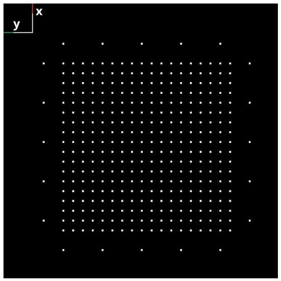
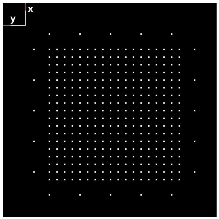
Secondly, once the pattern has been designed, the exposure conditions for different drawing elements in the pattern, such as spot size, magnification, dosage, dwell time, among others, are introduced into the Run File of the NPGS program, as described in Appendix A. Thirdly, once the run file has been created, the pattern can be written onto the substrate. The CAD drawing corresponding to this pattern is shown in Figure 3. Two kinds of samples were prepared: rectangular DNA origami of 90 nm × 70 nm with one silver-metalized NP, ~80 nm, attached at one corner, and another with two silver-metalized NPs, ~80 nm in size each, on opposite corners of the origami, as displayed in Figure 1. The samples were then ready for inspection by optical microscopy and SEM to assess the integrity of the EBL pattern and to identify selected lithographic sites suitable for dark-field microscopy.
Figure 3.
CAD design of a 100 μm × 100 μm pattern to write 100 nm × 120 nm rectangles, 5 μm apart, by electron beam lithography.
2.3. Dark-Field Microscopy
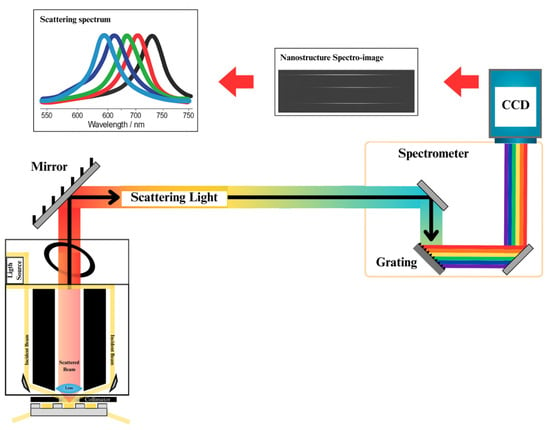
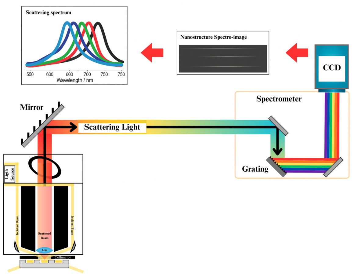
Far-field scattering provides a direct way to monitor localized plasmon resonances and near-field coupling in the metallic nanostructures studied here, because the optical response of a nanoparticle is strongly influenced by its geometry and local dielectric environment. Dark-field microscopy was used to visualize the Ag-metalized structures as bright scattering features against a low background. In the reflection configuration employed here, a dark-field objective delivered oblique white-light illumination to excite the localized surface plasmon resonance of the selected nanostructures. The experimental setup is schematically shown in Figure 4.
Figure 4.
Sketch of the dark-field spectroscopy setup. The CCD inset schematically illustrates the wavelength-dispersed image of the scattering signal from a single selected nanostructure.
Scattering images and spectra were acquired with a customized dark-field microscope (Nikon Corporation, Tokyo, Japan) equipped with a 100× 0.9 NA dark-field objective and a 75 W Xenon lamp (Oriel Instruments, Stratford, CT, USA). Samples were illuminated from above under dark-field conditions in the 400–700 nm spectral range. For spectral measurements, a 0.5 mm pinhole positioned at the image plane restricted the detected area to ~5 μm in diameter. During acquisition, this aperture was centered on a selected lithographic window, so that scattered light from a single registered measurement site was preferentially directed to the spectrometer, while contributions from neighboring sites or contaminants were minimized. Thus, the pinhole and the EBL-defined window array operate together: the lithographic pattern provides spatially registered candidate sites, whereas the pinhole provides optical readout from a single selected site at a time.
The collected broadband scattering was dispersed by the spectrometer grating and recorded on a liquid-nitrogen-cooled CCD camera (Photometrics CoolSnap HQ, Photo-metrics, Tucson, AZ, USA) coupled to an Acton SpectraPro 2300i spectrometer (Princeton Instruments, Trenton, NJ, USA). The CCD records a wavelength-resolved image of the scattering signal, from which one-dimensional spectra were extracted. Each raw spectrum was corrected by subtracting a background spectrum acquired from a nearby region of the SiOx/Si substrate without nanoparticles. The background-corrected signal was then normalized to the spectrum of white scattering standard (Labsphere Inc., North Sutton, NH, USA) to compensate for the wavelength-dependent response of the illumination path, spectrometer, and detector.
3. Results and Discussion
The samples were studied by three different microscopies: optical microscopy, scanning electron microscopy (SEM), and atomic force microscopy (AFM). The first two were used to inspect the integrity of the EBL pattern and the location of the metallic nanostructures within it. Optical microscopy is used to obtain a quick, rough picture of the patterns immediately after EBL writing. This technique provides a bird’s-eye view of how well the resist was lifted from the substrates and the resolution of the largest features in the patterns. On the other hand, SEM provides a more detailed visualization than optical microscopy, enabling proper characterization of the finest features. AFM allows a careful topographic and morphological analysis. The results obtained from these last two techniques are described below.
3.1. Morphological and Topographical Characterization
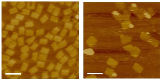
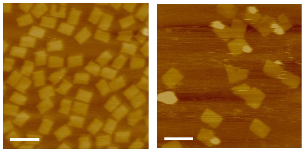
After synthesis, the structural integrity of the DNA origami nanostructures was probed by depositing them onto mica and Si/SiOx substrates. The morphological and topographical characterization of the nanostructures was performed using an atomic force microscope (Nanoscope II, Veeco Instruments Inc., Plainview, NY, USA) with NSG30 tips (NT-MDT BV, Apeldoorn, The Netherlands) in tapping mode. Freshly cleaved mica was first used to confirm both bare origami formation and the binding of one Au NP by AFM imaging in the same buffer used for DNA hybridization. According to the scale bar in Figure 5, the average measured dimensions of the DNA origami were ~70 nm × 90 nm, as expected. After drying the sample, AFM in air was used to verify Au NP attachment on an oxidized silicon substrate and to later proceed to silver metallization. Figure 6 shows an AFM micrograph in air of DNA origami functionalized with two Au NPs attached near opposite corners. This figure is included as a qualitative verification of Au NP attachment before silver metallization and before integration with the EBL-patterned substrate. The apparent lateral position of small Au NPs in AFM images may be affected by tip convolution, drying effects, linker flexibility, and possible deformation of the DNA origami on the characterization substrate.
Figure 5.
AFM micrograph of bare rectangular DNA origami, shown on the left, before functionalization. The scale bar is 200 nm. AFM micrograph of the rectangular origami after functionalization with one Au NP, shown on the right. The scale bar is 200 nm. In both images, the substrate is mica.
Figure 6.
AFM image of DNA origami functionalized with two Au nanoparticles before silver metallization. The image verifies AuNP attachment at the intended binding regions but is not used for quantitative analysis. The scale bar is 200 nm.
For the preparation shown, the yield of DNA origami structures containing the intended one- or two-AuNP configuration was estimated to be ~25% from the AFM fields inspected. This value should be understood as a sample-specific estimate and not as a general yield for all patterned substrates. The relatively low yield is likely related to incomplete hybridization of AuNPs to the selected binding sites, losses during washing and transfer steps, and possible disruption during drying or metallization. Future optimization of particle concentration, incubation time, buffer conditions, and surface chemistry may improve the fabrication efficiency and reproducibility.
3.2. Metallization Procedure and EBL Pattern
After AFM imaging, Au NPs bound to the DNA origami were enlarged in a controlled manner by electroless silver deposition to form metallic nanostructures. By this means, the Au NPs, 5 nm in size, serve as nucleation centers, with silver ions coalescing around their surfaces as the metallization time is varied. In this report, Au NPs fixed to the DNA assemblies, either at one corner or two opposite corners of the functionalized origami, were grown up to ~80 nm after 19 min of silver metallization. A detailed report on this process, including SEM images showing several stages of silver growth on the Au NPs, has been reported elsewhere [18]. Based on the nominal geometry of the rectangular DNA origami template, the designed separation between binding regions located near opposite corners is ~114 nm in this case. After silver metallization to an average particle diameter of ~80 nm, this nominal geometry corresponds to an estimated surface-to-surface gap of ~34 nm. This value should be regarded as a design-based estimate rather than a direct measurement of every individual dimer, since the actual interparticle spacing can be affected by linker flexibility, origami deformation, drying, and the silver growth process.
EBL is a first-class top-down technique for designing and patterning a SiOx/Si surface. In the present work, the EBL pattern is used to create spatially registered measurement sites for selected metallic nanostructures. This was done by creating an array of openings, or rectangular windows, nominally ~100 nm × 120 nm and spaced 5 μm apart, center-to-center, between adjacent openings. The 5 μm spacing was selected to be compatible with the optical field isolated by the image-plane pinhole during DFM measurements. The EBL-defined windows are therefore used as addressable sites for localization and optical interrogation.
The metallic nanostructures in solution were pipetted onto 5 mm × 5 mm oxidized silicon pieces with the EBL pattern displayed in Figure 3. For this purpose, a 20 μL drop of the metallic nanostructures at a concentration of 2 nM in solution was pipetted onto the EBL pattern. Afterward, the surface was washed with acetone to remove the photoresist, rinsed with DDI water, and carefully dried under a flow of N2 to eliminate any residual specks or impurities that might affect the plasmonic study by DFM. The nanostructures’ tolerance to acetone was also tested, and the results are shown in Appendix A. In total, four samples were prepared: two with metallic nanostructures containing one NP of ~80 nm in size, and two containing one NP at each of the opposite corners of the rectangular origami. This process does not guarantee deterministic filling of every lithographic site. Instead, the pattern provides an array of candidate measurement sites from which isolated target configurations can be identified by SEM and selected for dark-field spectroscopy. Empty windows, sites containing aggregates, and sites containing three or more nanoparticles were excluded from the optical analysis.
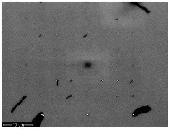
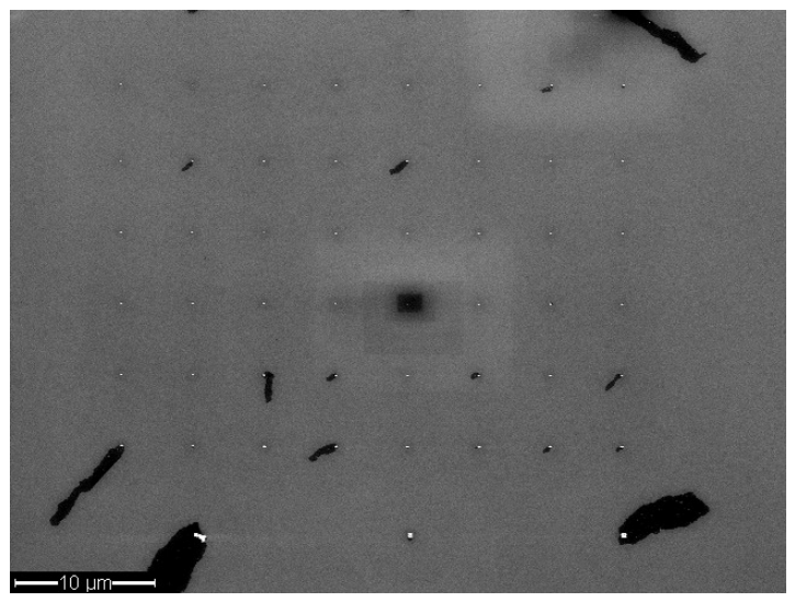
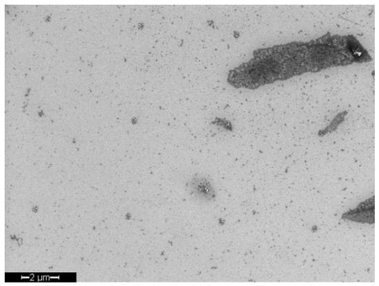
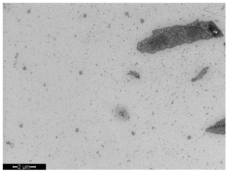
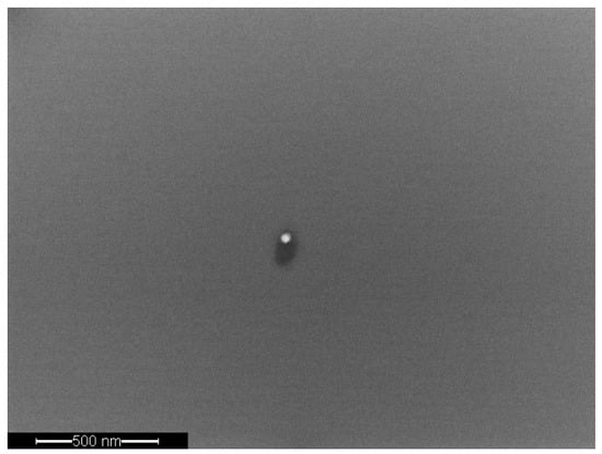
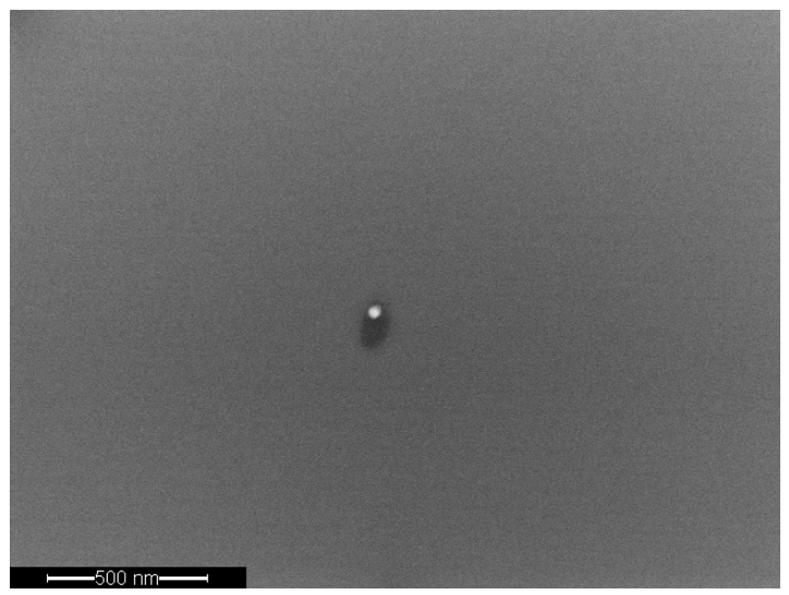
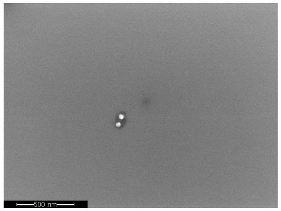
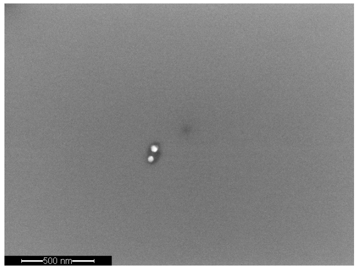
SEM was employed to characterize the apertures in the pattern and to identify lithographic sites suitable for DFM measurement. These results are presented in a series of SEM micrographs in Figure 7, Figure 8, Figure 9 and Figure 10. Figure 7 and Figure 8 show the periodic arrangement of the lithographic sites and illustrate the 5 μm spacing between neighboring windows. The relevant length scale for optical isolation is the 5 μm pitch between neighboring sites, which matches the detected field of view defined by the pinhole for DFM. Figure 9 and Figure 10 show high-magnification images of selected sites associated with one silver-metalized NP and with a silver-metalized NP dimer, respectively. For the dimer structures, the final lateral extension after Ag metallization can exceed the nominal 100 nm × 120 nm aperture; therefore, these structures are described as site-associated or window-registered rather than fully contained within the aperture.
Figure 7.
A SEM micrograph with dimensions of 54 μm × 37 μm, showing rectangular windows separated by 5 μm, patterned onto a SiOx/Si surface for the immobilization of metallic nanostructures.
Figure 8.
A magnified section of the SEM micrograph shown in Figure 7, with dimensions of 18 μm × 14 μm, displaying rectangular windows of ~100 nm × 120 nm, each containing a metallic nanostructure.
Figure 9.
A magnified SEM image showing a single silver-metalized Au NP, ~80 nm in size, immobilized within a rectangular window of ~100 nm × 120 nm on a SiOx/Si surface.
Figure 10.
A magnified SEM image showing a dimer of silver-metalized Au NPs, each ~80 nm in size, immobilized within a rectangular window of ~100 nm × 120 nm on a SiOx/Si surface.
An SEM-based occupancy examination was performed by direct visualization of the inspected patterned regions, by focusing only on the target nanostructures in all four samples. This statistical analysis indicates that on average, 32% of the analyzed windows contained a single nanostructure, 46% contained two or more nanostructures or aggregates, and 22% were empty (Table 1). These results support the interpretation of the EBL array as a site-selection and measurement platform rather than as a deterministic one-structure-per-window assembly method.
Table 1.
SEM-based occupancy distribution for the lithographically defined windows after metallic nanostructures deposition and lift-off.
3.3. Characterization by Dark-Field Microscopy
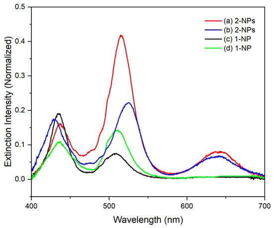
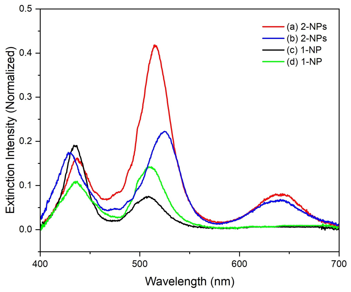
Finally, after SEM analysis, the samples were transferred to the DFM setup equipped with a spectrometer, as described in the Materials and Methods section. Dark-field spectra were acquired from selected lithographic windows containing the target nanostructure configuration. Empty windows, windows containing aggregates, and windows containing three or more nanoparticles were excluded from the spectral analysis. Figure 11 displays averaged extinction spectra obtained from four independently prepared samples, two of each kind. The red and blue curves, labeled 2-NPs(a) and 2-NPs(b), correspond to replicate samples designed to contain two Ag-metalized nanoparticles located at opposite corners of the DNA origami template. The black and green curves, labeled 1-NP(c) and 1-NP(d), correspond to replicate samples designed to contain one Ag-metalized nanoparticle located at one corner of the DNA origami template. Thus, the labels 1-NP and 2-NPs indicate the designed number of Ag-metalized nanoparticles per DNA origami template, whereas the letters (a–d) identify the independent samples measured by dark-field spectroscopy.
Figure 11.
Averaged extinction spectra obtained from four independently prepared samples of DNA-origami-templated Ag-metalized nanostructures. The labels 2-NPs(a) and 2-NPs(b) correspond to replicate dimer samples designed to contain two Ag-metalized nanoparticles at opposite corners of the DNA origami template. The labels 1-NP(c) and 1-NP(d) correspond to replicate single-particle samples designed to contain one Ag-metalized nanoparticle at one corner of the DNA origami template. Each curve represents the averaged spectrum obtained from selected lithographic windows containing the corresponding configuration.
The two 1-NP spectra and the two 2-NPs spectra provide independent replicates of the single-particle and dimer configurations, respectively. In both 1-NP samples, the main LSPR band appears in the 508–520 nm range, as expected for Ag-metalized nanoparticles with a diameter of ~80 nm. In the 2-NPs samples, an additional broad red-shifted contribution is observed in the 625–675 nm range, assigned to plasmonic coupling between the two Ag-metalized nanoparticles in the dimer configuration.
According to Mie theory [19], the localized surface plasmons (LSPs) in metallic spherical NPs strongly couple to fields in the visible region, producing intense scattered light [3]. For an isolated Ag sphere with a diameter close to 80 nm in air, classical Mie-type calculations and previous single-particle measurements predict a dominant dipolar localized surface plasmon resonance in the ~500–510 nm range, consistent with the experimentally observed 508–520 nm band. A weaker quadrupolar resonance is expected at shorter wavelengths, near the UV/near-UV region around 360 nm. Because the spectral acquisition window of the present dark-field setup starts near 400 nm, this quadrupolar feature is outside the accessible experimental range and was therefore not observed.
The sharp features observed between 431–436 nm should not be assigned to interband transitions of silver. Interband transitions in Ag occur in the UV spectral region and therefore cannot explain a peak near 430 nm [27]. The 431–436 nm contribution is more consistently associated with a secondary scattering contribution, such as window-edge/substrate scattering. In fact, it is expected that the depth of the EBL-etched windows on the oxidized silicon surface is about 50 nm and these indentations might serve as the engravings of a typical diffraction grating. Because its precise origin cannot be unambiguously determined from the present measurements, this feature is not used as evidence for the plasmonic response of the designed ~80 nm DNA-origami-templated nanostructures.
M. A. Garcia reports optical absorption spectra for Ag NPs of 40 nm embedded in a silicon matrix (n = 1.5), with well-resolved peaks at ~250 nm and ~410 nm [27]. The former peak was assigned to an interband transition, and the latter one to the LSP resonance of a single Ag NP. C. Sönnichsen reported measured scattering spectra in air (n = 1.0) for Ag NPs of different diameters, demonstrating a red shift and line broadening as the diameter increases. For instance, the peak of a 40 nm Ag NP shifts toward longer wavelengths as the diameter increases, reaching the ~500 nm region for particles having 80 nm in size [28]. Therefore, the features between 508–520 nm in Figure 11 are associated with the LSPR of the intended ~80 nm Ag-metalized nanoparticles. A small shift of about 12 nm is observed between the LSPR of the nanostructure with a single metalized NP, near 508 nm, and the corresponding one for a target nanostructure with a NP dimer, near 520 nm.
Furthermore, both samples with two neighboring Ag NPs per nanostructure exhibit broad peaks centered near 641 nm, in the red region of the visible spectrum. In review articles, A. P. Alivisatos et al. and Halas et al. reported that when the surfaces of two noble metal NPs are brought closer than their diameter, an electric interaction occurs due to the near-field induced by each NP [6,29]. As a result of this near-field interaction, the localized surface plasmons of the NPs couple. An indication of this plasmonic coupling is the splitting of the single-NP LSP resonance into two resonances as the NPs approach each other. In the transverse mode, the charge oscillations are perpendicular to the interparticle distance, whereas in the longitudinal mode, they occur along it. The peak position of the transverse mode in the scattering spectrum is almost imperceptible, while that of the longitudinal mode is clearly red-shifted [30]. In the present work, the additional broad band centered near 641 nm for the dimer configurations is attributed to plasmonic coupling between neighboring Ag-metalized NPs. The shift relative to the single-particle LSPR is ~120 nm. Similar values have been reported in the literature for plasmon-ruler systems and coupled noble-metal nanoparticle dimers [7,31,32,33]. The magnitude of the shift depends on the interparticle spacing, particle size, shape, composition, and dielectric environment [3,32,33]. In the present system, the center-to-center separation and the surface-to-surface gap should be interpreted as nominal design estimates rather than exact values for each individual dimer.
Last but not least, the 80 nm size of the metalized Au NP was chosen to ensure sufficiently intense light scattering from silver, which has the highest polarizability among the noble metals. According to electromagnetic theory, localized electric fields are mainly confined to the vicinity of metallic surfaces because of the plasmonic skin-depth effect. It has been assumed in this work that the NPs are composed of silver, even though the metallization process resulted in a bimetallic NP due to the coalescence of silver around a 5 nm Au NP core, producing a final particle with a diameter of 80 nm. This assumption is justified because the skin depth of a pure Ag NP is , which is smaller than the radius of the metalized NP over the 400–700 nm spectral range [34].
4. Conclusions
In conclusion, we have demonstrated a hybrid bottom-up/top-down methodology for the plasmonic characterization of selected individual DNA-origami-templated metallic nanostructures. DNA origami defines the nanoscale arrangement of the metallic nanoparticles, whereas the EBL-defined window array provides spatially separated and addressable sites for correlative SEM inspection and dark-field spectral acquisition. The 5 μm pitch of the array was designed to match the optical isolation imposed by the image-plane pinhole for DFM, allowing one selected lithographic site to be interrogated at a time. Therefore, the EBL array should be understood as a lithographically registered measurement architecture rather than as a deterministic nanoparticle-positioning scheme. Using this platform, the spectral response was evaluated in four independently prepared samples: two replicate samples containing one Ag-metalized nanoparticle and two replicate samples containing Ag-metalized nanoparticle dimers per each DNA origami template. The single-particle configurations exhibited main LSPR features in the 508–520 nm range, whereas the dimer configurations exhibited an additional broad band centered near 641 nm. This red-shifted spectral contribution is consistent with plasmonic coupling between neighboring Ag-metalized nanoparticles in the dimer configuration.
The reported approach here is presented as a proof-of-concept methodology. A full statistical optimization of the window-filling yield and of the distribution of interparticle distances is beyond the scope of the present work. Nevertheless, the results demonstrate that lithographically defined windows can provide useful spatial references for locating, selecting, and optically interrogating individual target DNA-origami-templated metallic nanostructures. This strategy provides a viable route for integrating programmable self-assembled nanostructures with lithographically defined measurement architectures for future plasmonic and nanophotonic studies.
Author Contributions
Conceptualization, E.C.S.; methodology, E.C.S.; software, E.C.S.; validation, E.C.S. and J.P.R.; formal analysis, E.C.S.; investigation, E.C.S.; resources, E.C.S.; data curation, J.P.R.; writing—original draft preparation, E.C.S.; writing—review and editing, E.C.S. and J.P.R.; visualization, E.C.S. and J.P.R.; supervision, E.C.S. and G.S.; project administration, E.C.S.; funding acquisition, E.C.S. All authors have read and agreed to the published version of the manuscript.
Funding
This research was funded by the Secretaría de Ciencia, Humanidades, Tecnología e Innovación (Secihti) through the CB-176352 project. The APC was funded by the Secretaría de Ciencia, Humanidades, Tecnología e Innovación (Secihti).
Institutional Review Board Statement
Not applicable.
Informed Consent Statement
Not applicable.
Data Availability Statement
The data presented in this study are available from the corresponding author upon reasonable request.
Acknowledgments
The authors are thankful to David R. Smith and his group from the Department of Electrical and Computer Engineering at Duke University in Durham, NC, for allowing us to use their facilities for the dark-field microscopy measurements.
Conflicts of Interest
The authors declare no conflicts of interest.
Abbreviations
The following abbreviations are used in this manuscript:
| DNA | Deoxyribonucleic acid |
| SiOx/Si | Silicon oxide on silicon |
| PMMA | Poly(methyl methacrylate) |
| CAD | Computer-aided design |
| DDI | Distilled, deionized |
| NPGS | Nanometer Pattern Generation System |
| EBL | Electron Beam Lithography |
| DFM | Dark-field microscopy |
| LSPR | Localized surface plasmon resonance |
| NP | Nanoparticle |
| SEM | Scanning electron microscopy |
| AFM | Atomic force microscopy |
Appendix A
Appendix A.1. EBL Procedure
Pieces of squared silicon wafers, 5 mm × 5 mm, covered with a 1 μm-thick layer of silicon dioxide (SiOx/Si), were used as substrates. They were cleaned using the standard RCA cleaning method [35] and plasma ashing [36] to remove spurious species, such as organic material, from the substrate surface. RCA cleaning is a set of standardized steps for thoroughly scrubbing silicon wafers. The first step, named SC-1, involves immersing the samples in a 1:1:5 solution of NH4OH (28%) + H2O2 (30%) + H2O at 80 °C for 10 min. The second step, named SC-2, consists of plunging the samples into a 1:1:6 solution of HCl (37%) + H2O2 (30%) + H2O at 80 °C for 10 min. This last step removes all ionic compounds from the substrate surface. A plasma asher (Plasma Prep III Plasma Cleaner, SPI Supplies Inc., West Chester, PA, USA) uses oxygen plasma to remove organic material that persists after RCA cleaning. Oxygen-free radicals react with organic compounds; the resulting carbon oxides and water vapor are volatile and pumped out of the chamber where the oxygen plasma takes place. A mass flow rate of 5 sccm for 5 min was allowed into the plasma asher to clean and increase the hydrophilicity of the substrate surface.
Once the substrates had been cleaned, a film of polymethyl methacrylate (PMMA) as a positive resist was applied to their surfaces by spin coating. PMMA is a polymer whose solubility changes upon exposure to an electron beam. The solution of PMMA diluted in anisole used in this work to cover the surface of the substrates was PMMA-A2 (2% of PMMA in anisole). The resist was deposited using a PWM32-PS-R790 spin coater (Headway Research Inc., Garland, TX, USA). The resist film was uniformly spread onto the substrate surface at 3000 rpm for 5 min. Subsequently, the substrates were placed on a hot plate at 200 °C for 90 s to evaporate the solvent (anisole). According to these conditions, the final thickness of the resist film was ~50 nm, as described elsewhere [37]. The resist surface was then exposed to an e-beam to etch the pattern, which was previously designed by CAD and NPGS. In our case, the EBL system was a commercial SEM Model XL30 SEM-FEG (FEI Company, Hillsboro, OR, USA), with the NPGS software as the interface, equipped with an electrostatic blanker to focus and deflect the e-beam to write the desired pattern as accurately as possible. To find the optimal technical exposure settings in the EBL system for our application, an array of several features with different linewidths was patterned to test different dosages and dwell times, thereby obtaining the appropriate parameters with sufficient resolution to write “windows” with dimensions of ~100 nm.
These optimum exposure conditions were entered into the Run File of the NPGS program. Then, the resist surface on a 5 mm × 5 mm piece of silicon oxide on silicon (SiOx/Si) was exposed to an SEM electron beam to define the previously designed square pattern, as shown in Figure 3 of the Materials and Methods section. Afterward, the sample was developed by removing the resist from the exposed areas using methyl isobutyl ketone (MIBK) as the developer. After development, the metallic DNA origami nanostructures in solution were pipetted onto the substrate to associate the structures with the lithographically defined measurement sites. Two sets of samples were prepared: rectangular DNA origami of 70 nm × 90 nm with one silver-metalized NP of ~80 nm attached at one corner, and the same DNA origami with two silver-metalized NPs of ~80 nm each positioned at opposite corners. Finally, the samples were lifted off by removing the unexposed resist using acetone as the solvent. The samples were subsequently rinsed with distilled, deionized (DDI) water and dried under an N2 flow. In a previous experiment, the acetone tolerance of rectangular DNA origami deposited on a SiOx/Si surface was evaluated.
Appendix A.2. DNA Origami Endurance to Acetone
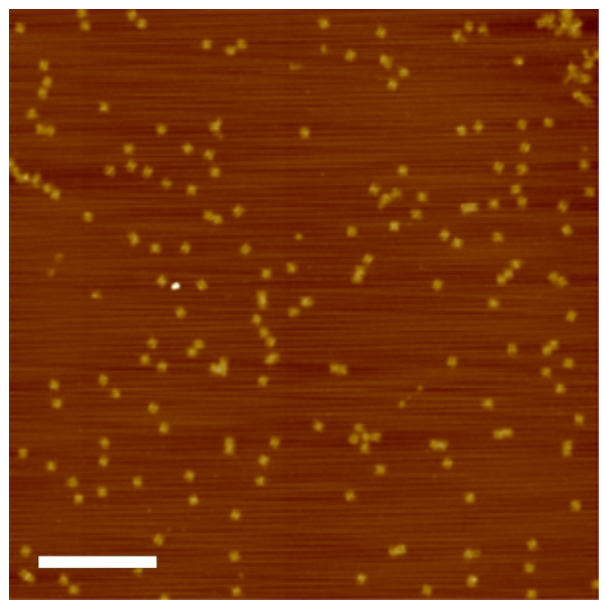
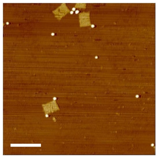
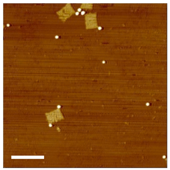
The persistence of the DNA origami in acetone was tested by rinsing the substrates with the nanostructures (no EBL pattern) using this solvent. This study was conducted on a square piece measuring 5 mm × 5 mm of a 1 μm-thick SiOx/Si layer, after the cleaning step described in the previous section. Firstly, the surface was rinsed in acetone for 10 s and dried with a cellulose-free paper towel. This stage was repeated, but the substrate was then dried with a flow of N2 to remove any impurity. A 5 μL drop of DNA origami with metalized NPs suspended in the TAE/Mg2+ buffer solution at a 2 nM concentration was deposited. The tolerance of the DNA nanostructures was assessed by immersing substrates with the nanostructures, without an EBL pattern, in acetone for 30 s. Later, they were rinsed with distilled deionized (DDI) water and dried using an N2 flow. These stages were repeated, but the substrate was now rinsed in acetone for 10 s. Afterward, the samples were visualized utilizing an AFM. Several regions of the sample were explored, taking images at 5 μm × 5 μm, as shown in Figure A1. The nanostructures were found to be complete and undamaged after rinsing the oxidized silicon substrates, demonstrating the tolerance of DNA origami to acetone, the solvent used in the EBL lift-off step.
Figure A1.
AFM micrograph of DNA origami after being rinsed in acetone. The scale bar is 1 μm.
References
- Atwater, H.A. The promise of plasmonics. Sci. Am. 2007, 296, 56–62. [Google Scholar] [CrossRef] [Scilit]
- Liu, J.; He, H.; Xiao, D.; Yin, S.; Ji, W.; Jiang, S.; Luo, D.; Wang, B.; Liu, Y. Recent advances of plasmonic nanoparticles and their applications. Materials 2018, 11, 1833. [Google Scholar] [CrossRef] [Scilit] [PubMed]
- Maier, S.A. Plasmonics: Fundamentals and Applications; Springer: New York, NY, USA, 2007. [Google Scholar]
- Stockman, M.I. Nanoplasmonics: The physics behind the applications. Phys. Today 2011, 64, 39–44. [Google Scholar] [CrossRef] [Scilit]
- Stelzer, E. Beyond the diffraction limit. Nat. Photonics 2009, 3, 361. [Google Scholar] [CrossRef] [Scilit]
- Choi, C.L.; Alivisatos, A.P. From artificial atoms to nanocrystal molecules: Preparation and properties of more complex nanostructures. Annu. Rev. Phys. Chem. 2010, 61, 369–389. [Google Scholar] [CrossRef] [Scilit] [PubMed]
- Jain, P.K.; El-Sayed, M.A. Plasmonic coupling in noble metal nanostructures. Chem. Phys. Lett. 2010, 487, 153–164. [Google Scholar] [CrossRef] [Scilit]
- Wen, X.; Deng, S. Plasmonic nanostructure lattices for high-performance sensing. Adv. Opt. Mater. 2023, 11, 2300401. [Google Scholar] [CrossRef] [Scilit]
- Tan, S.J.; Campolongo, M.J.; Luo, D.; Cheng, W. Building plasmonic nanostructures with DNA. Nat. Nanotechnol. 2011, 6, 268–276. [Google Scholar] [CrossRef] [Scilit] [PubMed]
- Matczyszyn, K.; Olesiak-Banska, J. DNA as scaffolding for nanophotonic structures. J. Nanophotonics 2012, 6, 064505. [Google Scholar] [CrossRef] [Scilit]
- Chen, Y.; Cheng, W. DNA-assembled plasmonic nanoarchitectures: From structural design to applications. WIREs Nanomed. Nanobiotechnol. 2012, 4, 461–478. [Google Scholar] [CrossRef] [Scilit] [PubMed]
- Chao, J.; Lin, Y.; Liu, H.; Wang, L.; Fan, C. DNA-based plasmonic nanostructures. Mater. Today 2015, 18, 326–335. [Google Scholar] [CrossRef] [Scilit]
- Gwo, S.; Chen, H.-Y.; Lin, M.-H.; Sun, L.; Li, X. Nanomanipulation and controlled self-assembly of metal nanoparticles and nanocrystals for plasmonics. Chem. Soc. Rev. 2016, 45, 5672–5716. [Google Scholar] [CrossRef] [Scilit] [PubMed]
- Liu, N.; Liedl, T. DNA-Assembled Advanced Plasmonic Architectures. Chem. Rev. 2018, 118, 3032–3053. [Google Scholar] [CrossRef] [Scilit] [PubMed]
- Liu, S.; Shang, Y.; Jiao, Y.; Li, N.; Ding, B. DNA-based plasmonic nanostructures and their optical and biomedical applications. Nanotechnology 2021, 32, 402002. [Google Scholar] [CrossRef] [Scilit] [PubMed]
- Niu, R.; Du, J.; He, W.; Liu, B.; Chao, J. DNA-based plasmonic nanostructures with tailored optical responses. Nano Res. 2025, 18, 94907197. [Google Scholar] [CrossRef] [Scilit]
- Zhan, P.; Peil, A.; Jiang, Q.; Wang, D.; Mousavi, S.; Xiong, Q.; Shen, Q.; Shang, Y.; Ding, B.; Lin, C.; et al. Recent advances in DNA origami-engineered nanomaterials and applications. Chem. Rev. 2023, 123, 3976–4050. [Google Scholar] [CrossRef] [Scilit] [PubMed]
- Pilo-Pais, M.; Goldberg, S.; Samano, E.; LaBean, T.H.; Finkelstein, G. Connecting the nanodots: Programmable nanofabrication of fused metal shapes on DNA templates. Nano Lett. 2011, 11, 3489–3492. [Google Scholar] [CrossRef] [Scilit] [PubMed]
- Mie, G. Beiträge zur Optik trüber Medien, speziell kolloidaler Metallösungen. Ann. Phys. 1908, 330, 377–445. [Google Scholar] [CrossRef] [Scilit]
- Zhang, W.; Zi, X.; Bi, J.; Liu, G.; Cheng, H.; Bao, K.; Qin, L.; Wang, W. Plasmonic nanomaterials in dark field sensing systems. Nanomaterials 2023, 13, 2027. [Google Scholar] [CrossRef] [Scilit] [PubMed]
- Ringe, E.; Sharma, B.; Henry, A.-I.; Marks, L.D.; Van Duyne, R.P. Single nanoparticle plasmonics. Phys. Chem. Chem. Phys. 2013, 15, 4110–4129. [Google Scholar] [CrossRef] [Scilit] [PubMed]
- Al-Zubeidi, A.; McCarthy, L.A.; Miandashti, A.R.; Heiderscheit, T.S.; Link, S. Single-particle scattering spectroscopy: Fundamentals and applications. Nanophotonics 2021, 10, 1621–1655. [Google Scholar] [CrossRef] [Scilit]
- Rothemund, P.W.K. Folding DNA to create nanoscale shapes and patterns. Nature 2006, 440, 297–302. [Google Scholar] [CrossRef] [Scilit] [PubMed]
- Samanta, A.; Medintz, I.L. Nanoparticles and DNA—A powerful and growing functional combination in bionanotechnology. Nanoscale 2016, 8, 9037–9095. [Google Scholar] [CrossRef] [Scilit] [PubMed]
- Chen, Z.; Liu, C.; Cao, F.; Ren, J.; Qu, X. DNA metallization: Principles, methods, structures, and applications. Chem. Soc. Rev. 2018, 47, 4017–4072. [Google Scholar] [CrossRef] [Scilit] [PubMed]
- Nabity, J.C. Nanometer Pattern Generation System: User’s Manual; Nabity Nanometer Pattern Generation System: Bozeman, MT, USA, 1992. [Google Scholar]
- Garcia, M.A. Surface plasmons in metallic nanoparticles: Fundamentals and applications. J. Phys. D Appl. Phys. 2011, 44, 283001. [Google Scholar] [CrossRef] [Scilit]
- Sönnichsen, C. Plasmons in Metal Nanostructures. PhD Thesis, Ludwig Maximilian University of Munich, Munich, Germany, 2001. [Google Scholar]
- Halas, N.J.; Lal, S.; Chang, W.; Link, S.; Nordlander, P. Plasmons in strongly coupled metallic nanostructures. Chem. Rev. 2011, 111, 3913–3961. [Google Scholar] [CrossRef] [Scilit] [PubMed]
- Gunnarsson, L.; Rindzevicius, T.; Prikulis, J.; Kasemo, B.; Käll, M.; Zou, S.; Schatz, G.C. Confined plasmons in nanofabricated single silver particle pairs: Experimental observations of strong interparticle interactions. J. Phys. Chem. B 2005, 109, 1079–1087. [Google Scholar] [CrossRef] [Scilit] [PubMed]
- Sönnichsen, C.; Reinhard, B.M.; Liphardt, J.; Alivisatos, A.P. A molecular ruler based on plasmon coupling of single gold and silver nanoparticles. Nat. Biotechnol. 2005, 23, 741–745. [Google Scholar] [CrossRef] [Scilit] [PubMed]
- Jain, P.K.; El-Sayed, M.A. Surface Plasmon Coupling and Its Universal Size Scaling in Metal Nanostructures of Complex Geometry: Elongated Particle Pairs and Nanosphere Trimers. J. Phys. Chem. C 2008, 112, 4954–4960. [Google Scholar] [CrossRef] [Scilit]
- Jain, P.K.; Huang, W.; El-Sayed, M.A. On the Universal Scaling Behavior of the Distance Decay of Plasmon Coupling in Metal Nanoparticle Pairs: A Plasmon Ruler Equation. Nano Lett. 2007, 7, 2080–2088. [Google Scholar] [CrossRef] [Scilit]
- Rodrigo, S.G.; García-Vidal, F.J.; Martín-Moreno, L. Influence of material properties on extraordinary optical transmission through hole arrays. Phys. Rev. B 2008, 77, 075401. [Google Scholar] [CrossRef] [Scilit]
- Reinhardt, K.A.; Kern, W. Handbook of Semiconductor Wafer Cleaning Technology, 2nd ed.; Noyes Publications: Norwich, NY, USA, 2008. [Google Scholar]
- SPI Supplies. SPI Plasma Prep™ III Plasma Cleaner. Available online: https://www.2spi.com/category/ppiii-plasma-cleaner/ (accessed on 26 May 2026).
- Nano™ PMMA and Copolymer Process Guidelines. Available online: https://smif.pratt.duke.edu/sites/smif.pratt.duke.edu/files/operating/EBL%20Resist%20Processes%206.pdf (accessed on 26 May 2026).

Disclaimer/Publisher’s Note: The statements, opinions and data contained in all publications are solely those of the individual author(s) and contributor(s) and not of MDPI and/or the editor(s). MDPI and/or the editor(s) disclaim responsibility for any injury to people or property resulting from any ideas, methods, instructions or products referred to in the content. |
© 2026 by the authors. Licensee MDPI, Basel, Switzerland. This article is an open access article distributed under the terms and conditions of the Creative Commons Attribution (CC BY) license.