


Abstract
Due to their remarkable long-term stability, variable bandgap, and relatively high absorption coefficient, copper indium gallium diselenide (CIGS) solar devices are among the most promising photovoltaic technologies due to their compatibility with lightweight substrates and special applications. This review critically discusses recent progress in the electrodeposition-based fabrication of CISe/CIGSe absorber layers, with special focus on electrolyte chemistry, electrochemical deposition mechanisms, precursor composition and morphology, post-deposition selenization/sulfurization, absorber quality, and photovoltaic device performance. We discuss aqueous and non-aqueous electrolytes, one-step and sequential electrodeposition, pulse-based deposition techniques, compositional control, film quality enhancement, Cd-free buffer layers, and large-area processing. The issues arising from the varied electrochemical behaviors of Cu, In, Ga, and Se are discussed, with specific emphasis on hydrogen evolution, limited integration of Ga, development of secondary phases, inhomogeneity of precursors, and process reproducibility. We review recent progress in device performance and explain typical manufacturing methods, and we summarise the key criteria for scaled electrodeposition. This review therefore sets up an integrated processing–structure–performance perspective for the further development of efficient and industrially relevant electrodeposited CIGSe solar cells.
1. Introduction
Due to increasing energy demand, scientists are increasingly exploring novel energy sources. Solar energy is becoming increasingly prevalent as a primary renewable energy source. This is a significant aspect of the development of abundant renewable technologies that use sunlight and heat, including artificial photosynthesis, thermal energy, solar heating, photovoltaics, and solar architecture. Furthermore, the generation of photocurrent when semiconducting materials are illuminated is commonly observed in active solar technologies that convert sunlight into energy. A standard photovoltaic system uses solar panels composed of many solar cells that generate electricity, such as solid films. The initial generation of solar cells is built on silicon wafers. They evolved from single-crystalline silicon (mono-Si) to polycrystalline silicon (multicrystalline Si). They now account for around 90% of the global market. Their efficiency in converting power ranges from 12% to 16%, depending on their wafer quality and fabrication process [1]. Even though mono-Si devices are very efficient and the most popular on the market, researchers are looking for a better option because the purification process is too expensive, fault tolerance is too low, and the band gap is indirect (meaning that they do not absorb as much light). Achieving high-efficiency CIGSe solar cells also requires intentional doping, alkali-metal inclusion, defect engineering (intrinsic and extrinsic), impurity control, grain-boundary passivation, and comprehensive interface-defect chemistry [1]. Where these issues have an immediate bearing on electrodeposition or post-deposition treatment, we briefly address them. Nevertheless, specialized studies addressing CIGSe defect physics and impurity engineering would be better suited than this review to thoroughly evaluate their electrical, atomic, and spectroscopic characteristics [2].
Most high-performance CIGSe devices to date have been manufactured via vacuum-based methods. These processes provide good control over film composition and quality. Still, they may be limited for large-scale deployment due to the high capital cost of vacuum equipment, target material requirements, energy consumption, and material loss during processing. Thus, non-vacuum fabrication techniques that lower processing costs while still providing appropriate control over absorber content and morphology have received much interest [3,4,5]. Electrodeposition is particularly attractive among these approaches since it is based on comparatively simple equipment, provides high material utilization, can be run over large substrate areas, and enables direct control through deposition potential, current density, electrolyte chemistry, and deposited charge. Furthermore, industrial and pilot-scale advancements have demonstrated the feasibility of electrochemically generated CIGSe precursors for integration in solar systems, strengthening the promise of electrodeposition for scalable thin-film manufacturing [6,7,8]. But with these benefits, electrodeposition of CIGSe is far more complicated than deposition of a single metal or binary compound. The electrochemical reduction potentials, reaction kinetics, and mass transfer behaviors of the four species in CIGS are considerably different. Ga’s addition in aqueous electrolytes is particularly challenging, because the reduction of Ga often occurs at very negative potentials, where hydrogen evolution and local changes in the interfacial pH are prominent. These actions may enhance oxide or hydroxide development, decrease current efficiency, and produce porous or compositionally inhomogeneous films [9]. Similarly, secondary phases can form by overinclusion of Cu or Se, and uncontrolled deposition of In and Ga can cause unwanted compositional gradients. Hence, the electrolyte composition, pH, complexing agents, deposition potential or current density, agitation, temperature, and pulse parameters have to be precisely coordinated to create homogeneous CISe/CIGSe precursors with controlled stoichiometry. Therefore, several approaches have been explored to enhance electrochemical control [10]. They are one-step co-deposition, progressive deposition of single or binary precursor layers, pulse-current and pulse-potential techniques, diluted electrolytes, complexing agents, nitrate-assisted deposition, and non-aqueous or deep-eutectic solvent systems. Pulse deposition can lessen the total current density by permitting ion replenishment during the relaxation phase, and complexing agents can diminish disparities between effective metal-ion reduction potentials. Non-aqueous electrolytes have larger electrochemical windows and can suppress competing hydrogen evolution. An alternate route is sequential deposition. In this case, the amount of each metal component can be adjusted independently before the subsequent thermal conversion [11,12,13].
Electrodeposition of CIGSe has been confirmed on scientific and technological grounds through several key reviews. Lincot [12] provided a general review of semiconductor electrodeposition, with an emphasis on the basic electrochemical principles of nucleation, development, and compound-semiconductor formation. Later, Saji et al. [13] examined progress on electrodeposited CuIn1-xGaxSe2 absorber layers and summarised the major electrolyte systems, deposition methods, compositional control approaches, and absorber processing developments reported at that time. Further studies on electrodeposited Cu(In,Ga)(Se,S)2 (CIGSS) for photovoltaic applications were performed by Bermudez [14], with an emphasis on improvements in precursor production, post-deposition conversion, and device fabrication. In a review of flexible CIGS photovoltaic technologies, Park and Jo [15] covered material and substrate selection, device and panel implementation, and more recent developments in flexible processing and mechanical performance. Together, these works illustrate the stepwise evolution of CIGSe technology from basic electrodeposition chemistry to absorber optimization, device integration, and scalable photovoltaic systems. By contrast, Ramanujam and Singh [16] provided a much broader review of CIGS photovoltaics, discussing absorber growth by a range of deposition technologies, band-gap grading, sodium effects, buffer layers, flexible devices, efficiency, stability, and commercialization; electrodeposition was thus only one of several fabrication approaches discussed [16].
This review presents an updated and focused examination of the processing–structure–performance of electrodeposition compared to the above-mentioned work. Special emphasis is placed on electrolyte chemistry and metal-ion speciation, electrochemical reduction and co-deposition mechanisms, aqueous and non-aqueous electrolyte systems, one-step and sequential electrodeposition, pulse-current and pulse-potential approaches, mass-transfer effects, hydrogen evolution, compositional control, precursor morphology, secondary-phase formation, substrate pre-treatment, and post-deposition selenization or sulphurization. The review also discusses the effect of these parameters on absorber crystallinity, compositional homogeneity, device architecture, photovoltaic performance, process repeatability, Cd-free device integration, and wide-area production [16,17]. This review is structured into eight sections that highlight key findings in the research area of CISe/CIGSe film electroplating research.
The scope of this review is purposely restricted to events directly related to the electrodeposition and subsequent transformation of CISe/CIGSe precursors. Therefore, detailed atomistic defect physics, intentional doping strategies, alkali-metal diffusion mechanisms, impurity segregation, advanced grain-boundary and interface-defect modeling, mechanical modeling of flexible devices, tandem-cell design, artificial-intelligence-assisted process optimization, full techno-economic analysis, and life-cycle assessment are out of the principal scope. They are only mentioned if they directly influence electrodeposition, precursor conversion, absorber quality, or the performance of the finished device. These boundaries delineate a processing–structure–performance framework to highlight the critical scientific and technological needs for reproducible, scalable, and ecologically sustainable electrodeposited CIGSe photovoltaics [16,17,18,19].
2. Device Structure and Material of CIGS
2.1. Structure of CIGS Complete Device
A substrate- or superstrate-based architecture is typically used for CIGS solar devices. The substrate configuration is the most popular since it works well with flexible metallic foils and can be processed at high temperatures. A conventional CIGS photocell is composed of a multilayered structure that maximizes light absorption, charge separation, and carrier collection.
The following layers typically make up the device structure (Figure 1):
Figure 1.
CIGS device layer structure.
- a.
- The Substrate
Conventional substrates include soda-lime glass (SLG), stainless steel, and molybdenum-coated polyimide. SLG is widely used in high-efficiency devices due to its beneficial diffusion of Na+ ions, which promote CIGS grain growth and defect passivation [1].
- b.
- Molybdenum (Mo) Back Contact Layer
The back contact layer is Mo deposited by sputtering. The Mo layer forms an ohmic contact with the CIGS absorber and provides high electrical conductivity and chemical stability during heating. To prevent peeling and cracking, its adhesion and stress must be properly managed [1].
- c.
- The CIGS Absorber Layer
Photon absorption and carrier production take place in the core functional layer, which is the p-type layer of the CIGS absorber. The Ga/(Ga + In) ratio can be adjusted to regulate the bandgap within the range of approximately 1.0 to 1.7 eV. This allows bandgap grading to enhance carrier collection and reduce recombination. Large particle size, high crystallinity, and a Cu-poor surface composition are required for optimal outcomes [1].
- d.
- Buffer Layers (CdS or Other Buffers)
The CIGS absorber and a thin buffer layer of n-type CdS created by chemical bath deposition (CBD) form a p–n junction. CdS offers advantageous interface passivation and band alignment. To address Cd toxicity, substitute CIGS device buffer layers, such as ZnS, Zn(O,S), and In2S3, have been developed; they exhibit good transparency and reduced parasitic absorption [1].
- e.
- Window Layer (Al-Doped ZnO/i-ZnO)
To protect the junction against shunts, intrinsic ZnO (i-ZnO) is applied on top of the buffer layer. The final conductive transparent oxide (TCO) is often Al-doped ZnO (AZO). As the front contact, the AZO layer offers low sheet resistance and great transparency [1].
- f.
- Anti-reflective coatings and the front electrode help reduce optical losses. A thin anti-reflective coating (ARC), such as MgF2, can be used. To further lower series resistance, especially in large-area modules, metal grid fingers are added in certain layouts [1].
2.2. Crystal Structure of CIGS Absorber Layer
Figure 2 illustrates the quaternary CuInGaSe2 tetragonal chalcopyrite structure, in which the atomic positions of the In and Ga atoms are identical, and they are formed by the intermixing of ternary CISe and CGSe of the I–III–VI group (I = Cu, III = In, Ga, and VI = Se), as illustrated in Figure 2 [14]. The crystal structure can be described by a twofold unit cell of zinc-blend composition with alternately arranged Cu and In atoms [20]. Each Se atom is paired with two Cu and two In atoms, and each Cu or In atom is tetragonally bound to four Se anion atoms. The binding strength between I-VI and III-VI varies, which may lead to lattice distortion, and thus, the lattice constants (c and a, where a’ is the lowest dimension and ‘c’ is the cell height) do not always have the intended value of 2:1 (c/a ratio) [21]. The departure of the (c/a) value from 2:1 indicates the extent of distortion. The ratio is around two for pure CuInSe2. However, as Figure 2 illustrates, the deviation of the c/a standard ratio toward decreased values is due to grain refinement because Ga atoms are placed as part of the main structure [21].
Figure 2.
Quaternary CuInGaSe2 (CIGS) tetragonal chalcopyrite structure.
Cu-d and Se-p state contributions to the valence-band area control the electronic structure of CIGSe, while group-III dominates the conduction band’s lowest (In/Ga) states [22]. Chalcopyrite-based absorber components, which are direct-bandgap semiconductors with an optical absorption coefficient of α = 105 cm−1, can be used to create p-type “absorber” layers in thin-film solar cells. The Cu-poor CIGSe chalcopyrite absorber (with a composition of Cu/(In + Ga) or CGI ratio < 1 and Ga/(In + Ga) or GGI ratio = 0.25–0.35) contains numerous imperfections, most likely Cu vacancies (VCu) and InCu or GaCu antisites [23,24]. In the Cu-poor CIGSe, the In2+Cu antisites couple with copper easily (Figure 3).
Figure 3.
Scheme of structured vacancy compound (OVC) in Cu-deficient CIGSe. The scheme demonstrates a chalcopyrite-type lattice comprising ordered copper vacancies and group-III antisite defects, denoted as or . A representative neutral defect complex is , whereas the comparable Ga-containing complex is . The ordered arrangement of these defects may result in Cu-deficient OVC phases such as CuIn3Se5, CuIn5Se8, and Cu2In4Se7 and related Ga-substituted compounds. Reasonable Cu deficiency can support p-type conductivity, whereas excessive vacancy ordering may increase recombination and decrease the open-circuit voltage [22,23,24].
Cu-poor CIGSe absorbers often include ordered vacancy compounds that are created by the periodic ordering of Cu vacancies and group-III antisite defects. A representative neutral defect complex is 2VCu− + InCu2+ or the analogous Ga-containing combination 2VCu− + GaCu2+. Two negatively charged Cu vacancies balance out one positively charged In or Ga atom at the Cu lattice position in these compounds. Cu-deficient phases like CuIn3Se5, CuIn5Se8, and Cu2In4Se7 and related Ga-substituted compounds may appear when such defects become spatially organized [22,23,24] (Figure 3).
Figure 3 shows that ordered vacancy compounds have often been observed on the surface of Cu-poor CIGSe absorbers and at the absorber/buffer interface. A slight Cu deficiency is beneficial since shallow Cu vacancies enhance p-type conductivity and may facilitate junction formation. However, a significant Cu deficit increases the density of antisite defects, organized vacancy phases, and deep recombination centers. Imperfections may cause carrier recombination, Fermi-level pinning, and lower open-circuit voltage. Thus, control of the Cu/(In + Ga) ratio is crucial to optimize beneficial vacancy-mediated p-type conductivity while suppressing deleterious defect-complex formation [22,24].
Another important bond-structure challenge is the 2V Cu in Cu-poor CIGSe, which leads to a neutral imperfection structure (2VCu− + InCu2+) [24]. Nonetheless, the inbuilt p-doping of the CIGS film absorber is facilitated by a slight excess of shallow acceptors, such as VCu vacancies (with an energy level near the valence band). Ordered vacancy compounds (OVC) are the (2VCu− + InCu2+) clusters of neutral defects with an average composition of Cu2In4Se7, CuIn3Se5, CuIn5Se8, etc. [25]. At the CdS/CIGSe interface, OVCs are expected in the CIGS absorber. The random structure of chalcopyrite, having dispersed vacancies of copper or (2VCu− + InCu2+) pairs of defects, can be used to create OVC layers, which are thought to improve device performance [26]. However, a higher OVC concentration in CIGSe may cause defects related to excessive Cu deficiencies to form, including Ga at Cu (InCu or GaCu) anti-site-based defects, thereby lowering the device’s open-circuit voltage (VOC) [27]. Through Fermi-level pinning, sophisticated electron traps (InCu, GaCu, and their complex DX centers) limit the devices’ persistent photoconductivity effect (PPC) [28,29,30]. Light- and bias-induced variations in the electrical properties of CIGSe, such as red-blue lighting and persistent photoconductivity (PPC), are believed to arise from various defects, including the (VSe–InCu) divacancy defect complex, selenium voids (VSe), and copper interstitials (Ci). Under electrical bias or light, this di-vacancy complex (VSe–VCu) in p-type CIGS can change from a donor to an acceptor configuration, raising the hole concentration and acting as a recombination route for minority charge carriers (electrons) [31,32]. Potential oscillations in the material are thought to originate from the predominance of these inherent faults and compensations.
Figure 4 displays the schematic of the most advanced CIGS film structure, Mo/CIGSe/CdS/i-ZnO/Al–ZnO, along with the film’s consistent band diagram. A maximum claimed efficiency (η) of 21% has been observed for these devices [33]. Following a summary of the composition, characteristics, and developments of the separate multilayers, the device’s operating principle is presented.
Figure 4.
(a) Schematic cross-sectional architecture of a conventional CIGSe thin-film solar cell, illustrating the glass/Mo/CIGSe/CdS/i-ZnO/Al:ZnO/metal-grid structure, incident-light reflection losses, carrier generation in the absorber, and possible electron transport pathways toward the front contact or recombination at the back contact. (b) Schematic energy-band diagram of the corresponding CIGSe device comparing structures with and without double band-gap grading. The graded absorber produces a modified conduction- and valence-band profile and a back-surface electric field near the Mo contact.
Aluminum-doped zinc oxide ZnO, as the front-contact of the device, confirms that the device receives maximum light due to its high bandgap and optical transparency. In high-efficiency devices, the sputtered layers of i-ZnO/ZnO:Al are typically employed as window layers. Since ZnO is inexpensive, non-toxic, and abundant, it is considered the most attractive TCO with an optical spectral bandgap of Eg = 3.3 eV [34]. According to several reports, devices with intrinsic zinc oxide window layers show decent stability under heat stress. Furthermore, by addressing local inhomogeneity in the CIGSe absorber, the combination of both buffer/window i-ZnO/CdS reduces the electrical shunt routes in CIGS films [35,36]. The buffer layer of cadmium sulfide (CdS) has been deposited in the majority of high-efficiency CIGSe devices reported to date. Light up to 2.4 eV is transmitted to the P-CIGS layer via the CdS buffer to the N-type of the device (Eg = 2.4 eV). Nakada [37] reported that Cd incorporation into the Cu-deficient CIGSe surface can occur through substitution on Cu sites. The similar ionic radii of (~0.96 Å) and (~0.97 Å) favor the substitution of Cd2+ for Cu+. Because Cd2+ replaces monovalent Cu+, the resulting substitutional defect acts as a donor and is denoted as donor defects, where the superscript ‘+’ represents the effective positive defect charge relative to the host lattice rather than the oxidation state of Cd [37,38,39].
The infiltrated Cd creates a buried CIGSe/CdS homo-junction in the absorber inhomogeneity [40]. Therefore, conductivity inversion of the absorber from p-type (CIGS) to n-type (CdS) and Cd doping at grain borders are unavoidable. Additional noteworthy findings are also documented, including Cu–Cd interdiffusion at the CdS/CIGSe interface, the formation of Cu2−xSe secondary phases, alkali–oxygen (Na–O) impurity buildup at the interface, Cd–Se formations, Cd diffusion in CIGSe, and selenim–sulfur exchange within CIGS-CdS [39,40,41,42,43]. The contact at the junction of CdS/CIGS is still a contentious issue and needs further investigation.
A schematic Raman spectrum of CIGSe is shown in Figure 5, which was created utilizing the distinctive Raman peak locations documented in the literature. The picture does not depict an actually measured or theoretically computed spectrum; rather, it is meant to show the primary CIGSe vibrational modes and the locations of potential secondary-phase peaks. As shown in Figure 5, the inclusion condition of indium at lesser cathodic potentials is excess selenium relative to the CuSe phase [44]. The poor response of the Se(0) species results in higher surface electrical resistance, which limits the amount of In that can be incorporated via surface reactions (at lesser cathodic potentials) [45,46]. The generated Se(–II) elements react with In3+ to create indium selenides (In2Se3) under high cathodic potential, and they are assimilated into the expanding CuInSe2 film [45,46,47]. At higher species concentrations and electrochemical potentials, In3+ can also immediately decrease to form In(0). The typical CIGS layer thickness ranges between 1.5 and 2 µm. Observations reveal the presence of the Cu-deficient CISe phase (160 cm−1) and elemental Se(0) (260 cm−1), also referred to as OVC, and the CIS mode of A1 (177 cm−1). The peak shows the conductive Cu2Se phase at 260 cm−1 [47].
Figure 5.
Schematic Raman spectrum of CIGSe showing the characteristic vibrational bands of an electrodeposited CISe/CIGSe thin film showing OVC, CISe A1, and Se(0)/Cu2Se-related peaks.
Cu-poor ordered-vacancy compounds, such as CuIn3Se2 or analogous defect-ordered phases, may be responsible for a Raman signature around 150–160 cm−1. These Cu-poor phases may be present in small quantities close to the absorber’s surface and may aid the creation of favorable junctions [47]. On the other hand, a broad or intense peak in this area could indicate incomplete chalcopyrite phase development, severe Cu deficiency, or compositional disorder. Elemental selenium or Cu–Se secondary phases may be linked to features in the range of roughly 250–265 cm−1. While Cu2Se and comparable copper selenides may also provide peaks within a similar spectral area, elemental Se typically produces a Raman band around 250–260 cm−1. Excessive selenium inclusion, regionally Cu-rich deposition, or partial conversion during annealing can all result in the formation of these phases [48]. Conductive Cu–Se phases are typically not wanted in solar absorber layers because they can create shunting routes and promote detrimental carrier recombination, thereby reducing device performance. A high-quality CISe/CIGSe absorber should therefore show a dominant chalcopyrite (A_1) mode, with peaks associated with elemental Se, Cu2Se, and excessive ordered-vacancy compounds that are either absent or somewhat weak, as shown in the schematic spectrum in Figure 5. To verify phase purity and distinguish the chalcopyrite absorber from secondary phases, Raman spectroscopy should be interpreted alongside X-ray diffraction, compositional analysis, and microscopy [46,47,48].
The applied potential primarily determines the Gallium content level during the deposition of CIGS films for CuGaSe2 or CuInGaSe2. Ga species do not exhibit induced surface interactions of In(III) ions with the CuxSe phase, in contrast to indium. At lower or higher cathodic potentials, Ga is included either as Ga(OH)3 (caused by a local pH shift) [49,50,51] or as Ga2Se3 (caused by a reaction with H2Se). Figure 6 shows two primary diffraction peaks corresponding to the <112> and <220> planes, consistent with the crystal structure of CIGSe. Cu Kα radiation with a wavelength of λ = 1.5406 Å was used for X-ray diffraction analysis. The diffraction patterns are shown as a function of 2θ. The Cu(GaIn)Se2 composition of the deposited absorber layer was revealed by XRD; no additional peaks were observed. The desired CIGS crystallography is shown by the strongest diffraction peak at 26.81. The thickness of the CIGSe absorber layer was approximately 1.4 µm, which is enough to absorb 97.5% of the incoming light, as shown in Figure 6 [6]. The tetragonal chalcopyrite CIGS structure’s (112) and (220)/(204) planes are represented by major diffraction peaks. Polycrystalline CIGS absorber films frequently exhibit preferential crystallographic orientation, which is shown by the strong (112) reflection [6].
Figure 6.
Diffraction peaks of Cu K radiation demonstrating that the CIGS layer was formed from a low-concentration solution during a 30 min annealing period at 500 °C. The deposit composition obtained after 40 min at −0.76 V vs. NHE at 500 rpm is shown in the tabulated insets. The solution comprised 0.45 mM CuCl2.2H2O; 0.44 mM InCl3; 0.85 mM H2SeO3; 0.5 mM GaCl3; pHydrion (pH = 2); and 0.66 M LiCl as supporting electrolytes. Temperature = 20 °C [6].
Raman spectroscopy and X-ray diffraction provide complementary information for the assessment of phase purity and structural quality of electrodeposited CISe/CIGSe absorber layers. Raman spectroscopy can be used to identify the characteristic chalcopyrite vibrational mode and differentiate it from features associated with Cu-deficient ordered-vacancy compounds, elemental Se, and the secondary phases (Cu–Se), as shown in Figure 5. This is especially essential because some secondary phases may overlap with the main CIGSe diffraction peaks and hence be difficult to identify by XRD alone. The distinctive X-ray diffraction peaks of the annealed electrodeposited CIGSe layer are shown in Figure 6 as complementary information for this investigation, confirming the creation of the tetragonal chalcopyrite structure and its favored crystallographic orientation [6]. Thus, Figure 5 and Figure 6 illustrate the complementary use of Raman spectroscopy and XRD for phase identification, structural verification, and quality control of electrodeposited CIGSe absorber films [47,48,49,50,51].
2.3. Deposition Methodology
Electrodeposition is a low-temperature, non-vacuum technique for the preparation of CISe/CIGSe precursor layers and offers potential benefits in terms of material utilization, process cost, and large-area production. However, the electrochemical production of multicomponent CIGSe is difficult because Cu, In, Ga, and Se species have very variable reduction potentials and reaction kinetics, chemical speciation, and mass-transfer behavior [13,15]. Therefore, deposition potential or current density, electrolyte composition, pH, complexing agents, temperature, and hydrodynamic conditions have to be carefully managed to produce precursor layers with proper Cu/(In + Ga) and Ga/(In + Ga) ratios. In addition, these parameters affect hydrogen evolution, localized pH changes, hydroxide generation, secondary phase growth, surface shape and compositional homogeneity, all of which play a role in absorber creation during selenization or sulphurization and ultimately photovoltaic performance [51,52,53]. Because of the difference in refractive index (n), reflection loss may occur when light enters through the metal grid spacing and TCO (Al:ZnO/i-ZnO) in back-contact-arrangement CIGSe films (Figure 7). Anti-reflective coatings like MgF2 can be used to reduce these reflection losses [51]. When the devices are illuminated, the built-in electric field at the CdS/CIGSe heterojunction interface sweeps the produced electron–hole pairs through the appropriate contacts, resulting in photocurrent. This is the basic idea behind how the devices work.
Additionally, some electrons may travel toward the back contact (or an incorrect contact) and recombine. Adding a back-surface field—an extra energy barrier that prevents electrons from flowing backward—can prevent this. The GGI ratio can be changed to produce the bandgap gradient. The energy-band diagram of the CIGSe device with (dotted) and without double grading (continuous line) is displayed in Figure 7, which shows the energy-bandgap profile of the CIGS absorber layer used in the simulation. Double grading in the CIGS absorber layer has significantly enhanced the performance of single-junction CIGS cells, as demonstrated by simulation and experimental studies [51,52]. Readers can consult the referenced literature for comprehensive details on grading methods and their effects on device performance [53,54,55].
All of the high-efficiency devices reported to date have low bandgap values (1.15 eV—CuIn0.7Ga0.3Se2) and a final device stage that is Cu-poor, with GGI ratios of 0.3–0.35 and CGI ratios of 0.8–0.9. Since excessive Cu content can generate a copper–selenium secondary phase that is harmful to film performance, a modest rise in dopant atomic composition is recognized as Cu-rich (≥25% at wt%) [56]. Therefore, the total copper composition of the absorber, including the Cu–Se secondary phase, is referred to as Cu-rich stoichiometry. Despite having higher mobility, lower defect concentrations, better crystallinity, and less bulk recombination, Cu-rich absorbers were less efficient than Cu-poor devices [57]. Potassium cyanide (KCN) selective etching can be used to eliminate the excess CuxSe phase and enhance the performance of the Cu-rich device [58]. By controlling the doping level, the interface recombination issues common in Cu-rich CISe devices can be resolved. Simulation studies (Figure 7) show that lower doping contents (Na = 1016 cm−3) may reduce tunnel-assisted recombination at the interface by increasing the recombination barrier of the Fermi level and the valence band edge. The Se flux can be used to adjust the level of copper-rich doping devices. The efficiency of the copper-rich device was greater than that of the copper-poor CISe device, with η = 8.6% at lower selenium variation and η = 6.2% at extremely high selenium flux [59,60]. Additionally, a thin In-Se layer was deposited, yielding a device efficiency of 13.1%. By lowering interface recombination, this approach restores the open-circuit voltage loss [60]. Given that compositionally modified Cu-rich devices may be able to compete with Cu-poor ones in terms of efficiency, these results are encouraging.
Figure 7.
Influence of absorber composition and selenium-related treatments on the conversion efficiency of electrodeposited CuInSe2/CIGS solar cells. Cu-poor CISe devices with optimized composition, , , and a bandgap of approximately 1.15 eV. Column 2: Cu-rich absorbers prepared under a very high selenium flow. Column 3: Low selenium flux. Column 4 represents the thin In–Se interfacial layer [59,60,61].
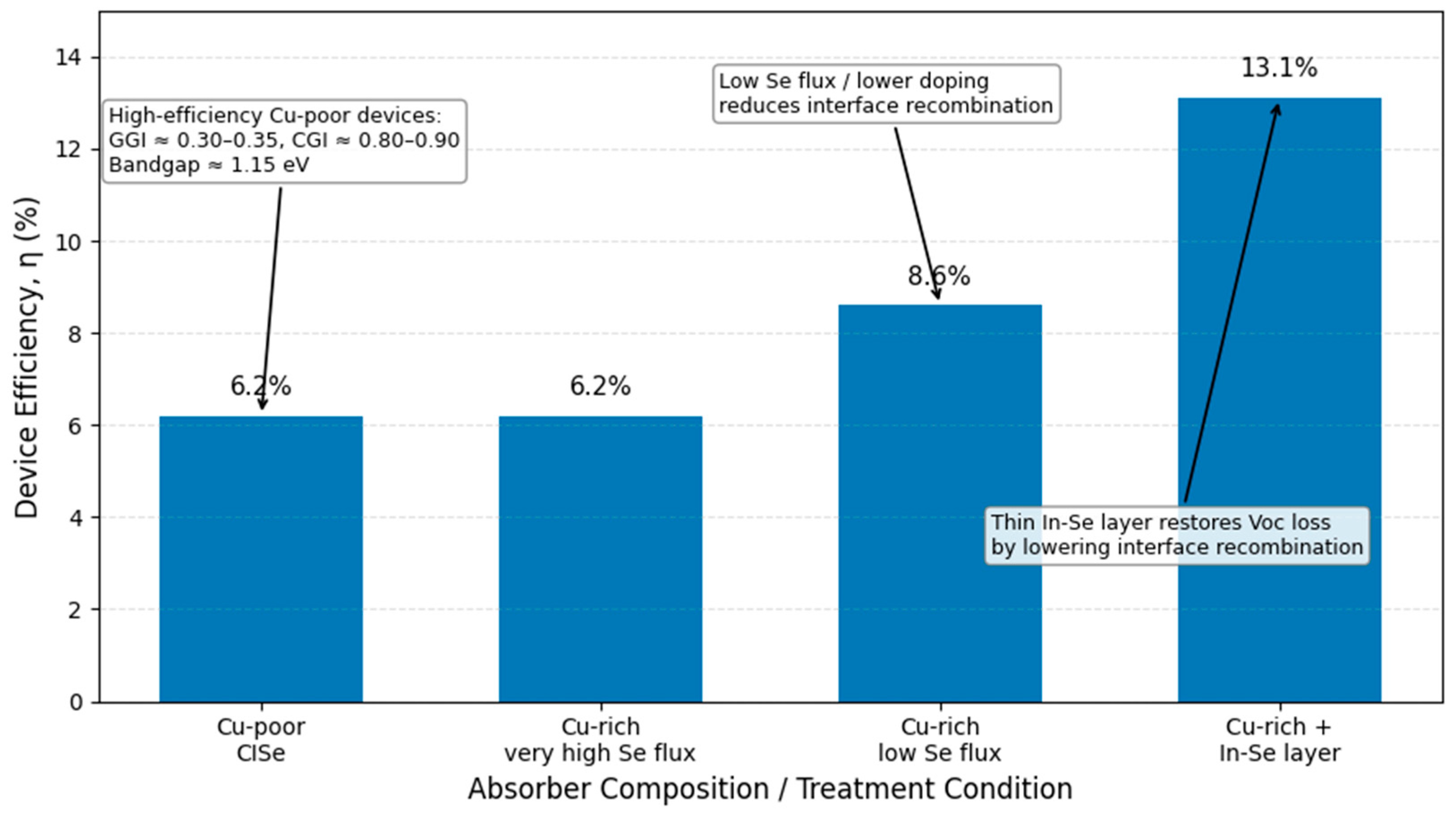
The development of CIGSe absorbers may focus heavily on compositionally modified Cu-rich absorbers in the future. Furthermore, compared to vacuum deposition, the electrochemical approach is significantly more straightforward to replicate in similar investigations. The relevant literature [61,62] discusses the most recent CIGS devices and a thorough recent evaluation of advancements in CIGSe solar cell fault processes.
3. Electrodeposition Methodology
3.1. Electrodeposition Parameters
3.1.1. Influence of Current Density and Applied Potential
The overall rate of electrochemical reduction is controlled by the current density, which substantially affects nucleation, growth, composition, and surface morphology. At relatively low current densities, deposition may be sluggish, and partial coverage of the substrate or integration of the more electrochemically active elements, especially In and Ga, may be insufficient. However, overly high cathodic potential can cause total current density, hydrogen evolution, local alkalization, and dendritic or porous development, which can limit improvements in the deposition rates of these species. In potentiostatic deposition, the ionic species reducible at the cathode are controlled by the applied potential. Cu and Se species typically deposit at less negative potentials than In and Ga; therefore, a sufficiently negative potential for In and Ga incorporation may also accelerate hydrogen evolution. Thus, the usable deposition window must be a compromise between co-deposition of the constituent elements, parasitic gas production, and low current efficiency [62].
The current or potential should not be chosen independently of the composition of the electrolyte. Complexing agents may change the effective reduction potentials of the four species and reduce the separation between their deposition ranges. This allows a multicomponent deposition under less harsh cathodic conditions and can diminish the preferred production of Cu-Se [61,62,63].
3.1.2. Role of Chemical and Electrochemical Potential
The electrochemical potential of each species depends on its thermodynamic tendency to be reduced and its activity in the electrolyte. It depends on the standard reduction potential, ion concentration, complex formation, pH, temperature, and interfacial electric field. Thus, the actual behavior of deposition may differ considerably from that expected based on typical reduction potentials alone. Phase development during deposition and subsequent chalcogenization is also influenced by the chemical potential of the CIGS species. A high copper chemical potential may favor the formation of conductive Cu-Se secondary phases, while a low Cu chemical potential may lead to the formation of very Cu-deficient ordered vacancy phases. Also, a lack of Ga chemical potential can lead to Ga-poor films, whereas excessive or non-uniform Ga incorporation can result in oxide/hydroxide phases or vertical compositional gradients. Therefore, the bath composition, complexation, applied potential, and deposited charge should be optimized to create a slightly copper-poor precursor with controlled Cu/(In + Ga) and Ga/(In + Ga) ratios [62,63].
3.1.3. Effect of Solution pH
The solution pH influences the speciation of metal ions, complex stability, hydrogen evolution, and oxide or hydroxide precipitation. Aqueous CIGSe electrodeposition is often performed under acidic conditions, since they allow In3+ and Ga3+ species to remain in solutions and hinder bulk precipitation. In very acidic solutions, however, the availability of protons increases, and the hydrogen evolution reaction is accelerated with appropriately negative potentials. The pH measurement at the cathode surface can differ markedly from the measured bulk pH. The hydrogen evolution and nitrate reduction reactions use protons or produce OH− at the electrode, raising local pH. This local alkalization may lead to incorporation of In and Ga as hydroxide or oxide intermediates rather than metallic species. These intermediates can be later transformed to the chalcopyrite phase upon reduction and selenization. Hence, stable pH control is necessary during the deposition process. Buffer systems, controlled agitation, diluted electrolytes, and pulse-off times can decrease local pH changes and improve composition and morphology [64].
3.1.4. Bath Temperature
Bath temperature affects ionic mobility, diffusion coefficients, electrolyte viscosity, complex stability, charge-transfer kinetics, and nucleation behavior. In aqueous electrolytes, mild temperature increases often boost mass transport and deposition kinetics. However, high temperatures can destabilize complexes, increase evaporation, expedite bath decomposition, or cause uncontrolled precipitation. Temperature management is especially crucial in non-aqueous electrolytes and deep eutectic solvents. Frequently, these media are highly viscous at room temperature. Heating lowers viscosity and enhances the movement of Cu, In, Ga, and Se species. Choline chloride–urea electrolytes are therefore generally used at temperatures of about 60–70 °C. But the temperature has to be maintained at a constant level because the film composition can be changed by variations in viscosity and diffusion even if the cathode-applied waveform remains the same [65].
3.1.5. Mass Transport Role
The replenishment rate of depositing ions is determined by mass transfer. If the deposition is continuous, one or more species will be quickly consumed, establishing a depleted diffusion layer and leading to high current densities. This can change the relative electroplating rates of the four species, leading to composition gradients or rough morphology. Agitation, electrolyte circulation, rotating-disk electrodes, substrate movement, and flow-assisted cells can improve ion replenishment. However, excessive agitation may destabilize initial nuclei or create non-uniform hydrodynamic conditions over large substrates. Mass-transfer conditions, coupled with current density, bath composition, and deposition duration, must be controlled and reported [6].
3.1.6. The Role of Pulse Deposition
Pulse current and pulse potential deposition alternate between a deposition period and a rest period. During the pulse-on time, electrochemical reduction and film growth take place. During the pulse-off time, depleted ions diffuse back to the cathode, partially restoring the interfacial concentration and reducing local pH gradients. The short pulse-on time promotes high nucleation density, and the sufficient pulse-off time prevents hydrogen evolution. But a very low duty cycle lowers the average deposition rate, and a high duty cycle is close to DC deposition and does not allow enough relaxation. Hence, pulse parameters should be optimized in conjunction with bath concentration, temperature, pH, agitation, and substrate conditions. Reproducibility is not possible by reporting merely pulse duration without specifying the peak current density, potential, or duty cycle [66].
3.2. Practical Issues Combined with Electrodeposition of CIGSe
The deposition of CIGS absorbers is typically accomplished in two ways, regardless of the synthesis route: either continuous electrodeposition and selenium/sulfurization or CIGS electroplating, followed by selenization or sulfurization [67]. Most vacuum deposition methods use simultaneous selenium deposition, while other processes, such as roll-to-roll printing, electrodeposition, and ink primer coating, use selenization. A significant challenge is the concurrent regulation of four-metal electroplating, given their varying reduction potentials, which complicates achieving the needed Cu-deficient and gallium-regulated composition. The presence of gallium is particularly challenging and may lead to undesirable Ga2O3 formation, internal flaws, and reduced conductivity if the local pH near the cathode is poorly regulated. The development of hydrogen during aqueous electrodeposition is a significant challenge, as it competes with metal-ion reduction, potentially leading to rough surfaces, pinholes, inadequate adhesion, and non-uniform films [68,69,70]. The deposition parameters, including current density, pulse-on/pulse-off duration, electrolyte concentration, pH, agitation, and complexing agents, must be meticulously optimized to prevent powdery deposits, secondary phases, inadequate crystallinity, and non-uniform thickness. The ultimate objective of any path, regardless of the deposition processes used in thin-film CIGSe/CISe production, is to obtain a compositional film with high crystallinity, yielding a material with good photovoltaic properties. In non-vacuum electrodeposition, ions at a specific reduction potential are reduced on a conductive substrate under an applied electric field to form thin films. The four metal ions in the electromotive force (EMF) series have the following equilibrium reduction potentials: +0.337/SHE, −0.342/SHE, −0.529/SHE, and +0.741/SHE. The decrease in the potential of the active standards of In3+ and Ga3+ ions is the cause of the difficulty encountered during CIGSe electrodeposition. The potential changes toward Cu(II) when In(III) and Ga(III) concentrations are increased [70]; however, excessive currents produced by high bath concentrations can seriously pit and corrode Mo/glass substrates [71]. Excessive ions may interact with or combine with the surface of molybdenum oxides, ultimately leading to some degree of Mo dissolution according to the latest impedance investigations carried out by a research group (Saji et al.) [71]. The efficiency of In and Ga plating is affected by electrodeposition at high cathodic potentials due to concurrent hydrogen evolution, which is thought to cause pinhole development and film inhomogeneity [72,73,74]. This further complicates the electroplating of stoichiometric and pinhole-free CIGS films. This deficiency developed because complexing agents added to In(III) and Ga(III) ions limited inclusion. Complexing agents can meaningfully raise the drop potential of copper ions toward that of active indium and gallium ions, simplifying co-electroplating. CIGS materials enhance the compactness of the deposited film, preventing pinholes and reducing hydrogen formation. Additional additives, including brighteners, surfactants, and supporting electrolytes, are frequently added to enhance bath chemistry and film quality [75]. The majority of complexing agents, however, only form strong complexes with copper and selenium ions and have little impact on Ga(III) or In(III) ions [10]. Significant recent developments in the deposition solution chemistry for the regulated ions of both In3+ and Ga3+ CIGS solar devices under aqueous and non-aqueous electrochemical process conditions are highlighted in the sections that follow [74,75,76].
4. Electrolyte Systems
4.1. Electrodeposition of CISe/CIGSe Utilizing Complexing Agents in Aqueous Solution
The one-bath electroplating of a CISe absorber layer using a complexing agent (triethanolamine (TEA)) was initially reported by Bhattacharya et al. [77]. Since then, a number of studies on the electrochemical plating of both CISe and CIGS using the TEA agent have been published, owing to its ability to form weak complexes with In3+ ions and strong complexes with Cu2+ and HSeO2– ions [78]. According to Calixto et al., pinhole-free stoichiometric CIGSe was electrodeposited in a bath at pH 2.5 using low concentrations of CuCl2*2H2O (2.56 mM), InCl3 (2.40 mM), GaCl3 (5.7 mM), and H2SeO3 (4.5 mM). Lithium chloride was used as a plating solution support, and a pH 3 buffer (pHydrion) for adjusting pH levels was used to stabilize the electrolyte [79]. According to recent research by Liu et al., the layer atomic ratio shifts from copper-rich to copper-poor with a rise in sodium sulfamate concentrations, whereas the (Cu + Se)/(In + Ga) ratio decreases with increasing gallium atomic ratios [80]. Cu2+ and Ga3+ have a reduction potential difference of just 80 mV. When KCN− was used as the complexing agent, the difference in potential was 870 mV for uncomplexed (Cu,Ga) species [80]. Cu(I) in a soluble form is the main species at high concentrations of the thiocyanate complex. Moreover, the presence of thiocyanate (CNS−) ions can catalyze the reduction of Ga. For CIGSe/CGSe electroplating, thiocyanate is therefore an appropriate complexing agent [81].
Even under high alkali conditions, by applying potassium sodium tartrate as a complexing agent for In ions and trisodium citrate for Ga ions, Aksu et al. were able to electroplate In–Se and Ga–Se films. At a pH of 13, a 68% plating efficiency for In–Se was achieved. When Ga–Se complexed with trisodium citrate, the Ga percentage was dominant at high pH values of 13.5, while the Se percentage dominated below pH 5. Ga–Se films could be co-deposited within a pH range of 7–8.5 [82]. Complexing agent blends are used to solubilize and inhibit the formation of hydroxide ions under such highly alkaline conditions, and they are also used to co-deposit a Cu–In–Ga layer (9–13.5). Common chelating agents including TEA, EDTA, citric acid, trisodium citrate, potassium sodium tartrate, and tartaric acid might be utilized because they form complexes with Cu, In, and Ga ions, even though the processing parameters were not stated. Modulating the current density during electroplating is another method for grading Ga [83].
According to the research group, an intriguing alternative method for adding Ga(III) and In(III) is to use the corresponding nitrate salts as oxides or hydroxides [84,85].
Nitrate reduction and oxide precipitation are two simultaneous stages that reduce indium and gallium during the process. Proton consumption during nitrate reduction causes a local pH shift near the surface cathode; the next step is the deposition of indium and gallium as precipitated oxides or hydroxides. Compared to Cu-In-Ga electroplating from conventional chloride/sulfate electrolytes, the deposition of In and Ga as oxides/hydroxides occurs at comparatively lower cathodic potentials, as illustrated in the usual deposition potential diagram (Figure 8). The crystalline CIGSe absorber that was deposited had a power conversion efficiency of η = 9.4% with additional hydrogen reduction and selenium pre-treatment (shown in Figure 8) [86].
Figure 8.
A comparison of the standard deposition potentials of gallium, copper, and indium as metals or hydroxide/oxide following nitrate reduction [82,83,84,85].
With respect to the application of hydrogen peroxide (H2O2) as the source of oxygen that facilitates Ga incorporation as Gallium(III) hydroxide (Ga(OH)3), according to Yang et al., the reduction starts with the cupric ion and moves on to the reduction of H2O2. This regulated Ga(III) ion inclusion includes In and Ga as oxides or hydroxides. At higher H2O2 concentrations (20 mM), where deposition occurs via kinetic control of hydroxide ions, precipitation of In and Ga was observed [87].
The experiment demonstrated that by altering the electroplating potential from a similar bath, it was possible to electroplate CIS (p, i, and n-type) [88] and CIGS (p+, p, i, n, and n+) [89] without the need for complexing agents or supporting electrolytes. Significant variations in the (Ga/III) concentration are the main obstacle to employing aqueous electrolytes, since even slight changes in the electroplating may affect the atomic ratio of the deposited film and, consequently, the deposition mechanism [90]. Therefore, the applied deposition potential significantly affects the film’s morphology. Balancing the composition and quality of a film is often difficult due to the limited deposition potential window, as illustrated in Table 1. Furthermore, the (Ga/III) atomic composition can be adjusted to an exact point, exceeding the limit at which hydrogen evolution (HER) occurs in parallel and adversely affects film quality, leading to dendritic morphology and pinhole formation [91]. The issue of hydroxide generation during traditional CuInGa electrodeposition is leveraged in metal-oxide/hydroxide depositions, which show greater promise. Using metal-oxide/hydroxide deposition, Ga inclusion in conventional CuInGa plating is a relatively solved issue [91].
Table 1.
Standard reduction potentials and typical cathodic reactions associated with CIGS electrodeposition in nitrate-based aqueous media.
Compared with traditional deposition methods, recent developments in solution chemistry for CIGS deposition, including (1) combinations of complexing agents, (2) nitrate precursor, and (3) the source of hydrogen peroxide, are encouraging, as they make it easier to overcome the issue of Ga inclusion. Additional research on electrolyte stability, ion replenishment, and electrolyte reuse may contribute to economical industrial-scale deposition processes [91].
Copper deposits are initially metallic. Given that Cu2+/Cu possesses a positive E° (~+0.34 V), copper can deposit as a metal prior to reaching the strongly cathodic region required for In/Ga. In and Ga metal deposition requires highly negative potentials, approaching or exceeding the threshold for H2 evolution in aqueous solutions. Nitrate reduction occurs at significantly lower potentials and produces OH−, thereby substantially increasing the cathode surface’s pH, even when the bulk pH remains moderate. Due to the exceedingly low solubility product constants (Ksp) of In(OH)3 and Ga(OH)3, a localized pH elevation to approximately 2–4 can initiate the deposition of hydroxide/oxide species of In and Ga at or near the cathode by chemical precipitation [89,90,91].
The practical implication for CIGS electrodeposition is that, in nitrate-containing solutions, a mixed mechanism is often observed. Copper can be electrochemically deposited as a metal; incorporation of indium and gallium is strongly influenced by nitrate-induced local alkalization, resulting in the formation of indium/gallium hydroxide/oxide intermediates, which must then be converted to the necessary chalcopyrite phase. The reduction of nitrate elevates local OH− concentrations, allowing In3+/Ga3+ to form hydroxide precipitates despite the thermodynamic and kinetic unfavorable conditions for metal deposition, as shown in Table 1 [90,91].
4.2. Electrodeposition of CISe/CIGSe in Non-Aqueous Electrolytes
Ionic liquids, ethylene glycol, and other non-aqueous electrolytes lack the presence of complexing compounds [91,92], and an ionic liquid mixture can be used to circumvent the HER interference. Combining LiCl electrolytes (pH 1.9–2.2) and alcohol, Long et al. demonstrated superior electroplating quality and produced convenient CIGS devices at −1.6 V/SCE [93]. In(III) and Ga(III) ion electrodeposition, the availability of such a broad electroplating window layer in non-aqueous deposition baths makes it convenient.
Ionic liquids have attracted attention for their wide electrochemical potential windows, biocompatibility, non-toxicity, and cost-effectiveness, which make them ideal electrolytes for electrodepositing elements that are challenging to plate under traditional aqueous-bath conditions [94]. In particular, aprotic deep eutectic solvents (DESs) and choline chloride (ChCl)-based ionic liquids have become effective substitutes for traditional ionic liquids. One of the commonly used DESs in CIGSe electrodeposition is reline, which is a combination of urea and choline chloride (ChCl/U = 1/2). Ionic liquids can achieve high solubility and reagent concentrations without water, in contrast to aqueous electrolytes, where the precipitation of oxides and hydroxides limits the solubility of metal ions. Furthermore, high ligand concentrations provide greater control over metal solubility in the electrolyte [95,96,97]. Consequently, reline and the ions form potent metal complexes, which eliminate the need for complexing agents. Even after extended hot conditions, reline remains extremely stable and does not break down. It is possible to improve the mass transport properties of ions by decreasing the viscosity (η) of reline. Because of this, the ideal bath temperature for electroplating is often kept between 60 and 70 °C [98].
Quaternary CIGS film electrodeposition in a single step employing reline was initially reported by Harati et al., with 65 °C set as the default temperature [99]. Steichen et al. described using reline at 60 °C to electrodeposit Cu–Ga thin films. The total-area power conversion efficiency of the selenium-treated CuGaSe2 photovoltaic cells, produced at 550 °C in the Se environment, was 4.1%. No alloying processes were seen when gallium or gallium and indium bilayer films were electroplated on back-contact Mo alone; instead, the resulting layers were discovered to be physical droplets of the In-Ga mixture (Table 2) [100]. On the other hand, producing a CuGa2 alloy substrate consisting of Mo/Cu was found to improve the adhesion of Cu–Ga films (Table 2) [100]. For pulse-current plating of a CIG ternary film, a reported efficiency of 10.1% was obtained for the CIGS film. Accelerated thermal treatment in an Ar environment for one hour at 550 °C was used to incorporate selenium (Se powder). By modifying the ion concentration flux ratio of [Ga3+/In3+] ions, Malaquias et al. demonstrated that it is possible to change the [Ga/In] ratio from 0 to 1 [Table 2] [101]. For CIGSSe thin films, the same group claimed an efficiency of 9.8%. After the In-Ga bilayer film was electrodeposited onto Mo/Cu back-contact films, a three-phase thermal treatment process using H2Se, Ar, and H2S was performed, as shown in Table 2 [98,99,100,101].
Table 2.
Non-aqueous electrolyte systems for electrodeposition of CIS/CIGS/CIGSe thin-film precursors.
5. Deposition Mechanisms
5.1. Challenges in CIGS Electrodeposition
A chalcopyrite semiconductor, copper gallium diselenide (CuGaSe2), has a relatively wide band gap (often reported near ~1.65–1.70 eV). This makes it appealing as a “Ga-rich end member” important for understanding Ga incorporation trends in CIGS, as well as a wide-gap absorber (e.g., for top cells in tandem concepts). Although CGS is notoriously difficult to electrodeposit in a single step due to the electrochemical challenges posed by Ga inclusion, low-cost electrodeposition is attractive because it can be scaled to large areas using inexpensive precursors and simple equipment. Reviews and the literature on electrodeposition for chalcopyrites highlight this difficulty [101].
5.2. Electrodeposition Conditions and Challenges
- (1)
- Ga inclusion versus hydrogen evolution: a fundamental electrochemical challenge
Very cathodic potentials are required for Ga2+ reduction in aqueous baths, and at low pH, these potentials are strongly opposed by hydrogen evolution (HER). Since Ga reduction peaks are weak or hard to see in cyclic voltammetry investigations of Cu–Ga–Se baths, Ga is usually the rate-limiting constituent in one-step CGS electrodeposition [102].
Practically speaking, pushing to more negative potentials can increase Ga content, but it can also destabilize stoichiometry, promote HER-induced defects, and increase roughness and porosity. The Ga atomic fraction, for instance, increased significantly with increasing negative potentials in acidic baths on ITO (approaching ~16 at.% at roughly −0.95 V vs. SCE in some systems), highlighting the potential-controlled character of Ga integration [102,103,104].
- (2)
- Complexing agents’ function: bringing reduction potentials closer together
One important tactic is to use complexing agents to “pull” the species’ reduction potentials closer together, particularly by cathodically shifting the Cu(II) reduction potential, thereby making Ga inclusion more practical in a single bath. One of the best-known examples is thiocyanate (SCN−), which can drastically alter the chemistry of Cu, leading, according to some publications, to a gap of just tens of mV between the peak currents of Cu and Ga in CV. This allows for wider stoichiometric windows and more controlled co-deposition [103].
In contrast to non-complexed or less appropriate settings, CV evidence indicates that some acidic/complexing situations can promote Ga uptake and make Ga reduction more detectable. Other complexing environments, such as acidic agents like hydrochloric or sulphamic systems, have also been investigated [102,103].
- (3)
- Enhancing mass transfer and composition management to support electrolytes and bath conductivity
Supporting electrolytes enhance ionic conductivity and can affect secondary-phase development and deposit composition, in addition to complexation. Lithium salts have been investigated as conductivity enhancers for Cu–Ga–Se electrodeposition; one accepted manuscript study reports that films deposited with lithium nitrate (as opposed to lithium chloride) showed atomic ratios closer to CGS stoichiometry (e.g., [Cu]/[Ga] and [Se]/[Cu + Ga] approaching ~1 with increasing LiNO3 concentration). However, morphology remained substrate-dependent [104]. This emphasizes a recurrent theme: while composition in ternary electrodeposition is frequently controlled by coupled kinetics, mass transport, and induced compound formation pathways, bath engineering (complexant + support electrolyte + pH) is just as crucial as potential selection [104].
- (4)
- Effects of the Substrate (ITO/FTO vs. Mo): Secondary Phases, Morphology, and Nucleation. Transparent conducting oxides (ITO/FTO) and Mo-coated glass (device-relevant) have both been shown to exhibit CGS electrodeposition. The choice of substrate affects adhesion, post-anneal microstructure, and nucleation density. When comparing Mo to FTO, for example, Mo can produce deposits with isolated tiny grains or voids under some circumstances, suggesting that substrate-specific tuning (additives, pulse plating, agitation, etc.) may be necessary to optimize nucleation and coalescence [104]. Secondary phases, especially Cu–Se phases, are a recurring problem in local conditions that are Cu-rich or Se-rich. After annealing, XRD may identify CuSe2 signatures but also reveal CGS peaks (e.g., (112), (204)), suggesting partial conversion or residual Cu–Se phase segregation, which may degrade electronic quality [103,104,105].
- (6)
- Post-Treatment (Annealing/Selenization): Creating Chalcopyrite CGS from Weakly Crystalline Deposits. One-step, as-deposited films frequently exhibit mixed or weakly ordered phases or low crystallinity. Chalcopyrite CGS is thus largely dependent on thermal treatment, usually annealing or selenium. It has been demonstrated that one-step water electrodeposition and annealing can “dramatically” increase crystallinity, resulting in polycrystalline CGS with a reported band gap of about 1.66 eV (and, when sulphurized, conversion to CuGaS2 with a larger band gap). Another method is to electrodeposit Cu–Ga metallic precursor layers (often in alloy form) and then anneal them in selenium vapor. When the precursor stoichiometry is properly managed, this method can provide improved control over the metal ratio before selenium incorporation and enhance absorber quality [105].
- (7)
- The Significance of Ionic Liquids and Deep Eutectic Solvents (DESs) for CGS Electrodeposition. Ionic liquids and deep eutectic solvents have become crucial for Ga-containing deposits because Ga is limited in aqueous systems and has a narrow electrochemical window. Ga deposition may continue in a choline chloride/urea DES (reline) with good plating efficiency and without HER interference; Cu–Ga precursor stoichiometry can be adjusted by hydrodynamic and potential control; CGS absorbers are formed by selenium annealing afterward. This technique has been shown to produce complete devices, with stated efficiencies of about 4% in representative trials [103,104,105]. Needle holes and poor morphology result from HER’s interference with the electrodeposition process. Table 3 provides the deposition characteristics for the one-step deposition process of CGSe films.Table 3. CIGS (or CGSe) electrodeposition conditions and resulting film compositions.
Potassium cyanide (KCN−) is an appropriate complexing agent for single-step electroplating of CuGaSe2 films according to recent research. A shift in Cu’s reduction potential toward more negative values facilitates the assimilation of Ga3+ ions in the form of Ga2Se3 during the formation of CuGaSe2 films. There have been reports of crack-free CGS thin films made of gelatin and lithium sulfate (Li2SO4). Successful electrodeposition of CGSe using DES, such as reline, has been documented. Another effective method for incorporating Ga as oxides or hydroxides is the electroplating of a Cu–Ga film using copper–gallium nitrate salts [105,106,107].
5.3. Electrodeposited CIGSe Thin Film Quality
The thin CIGSe layers must be devoid of surface imperfections, voids, cracks, and molecular inhomogeneities to be produced on an industrial scale via electrodeposition of CIGSe. This section covers documented experimental methods for enhancing CIGSe absorber quality for excellent performance systems [108]. Precisely controlling electrolyte composition and deposition potential is one of the most crucial tactics. The concentrations of the four species in the deposition bath can be adjusted to modify the final CIGSe composition. For instance, while Se2+ concentrations significantly affect both Se incorporation and metal content, increasing Cu2+ concentrations tend to increase Cu content [108,109,110]. To create Cu-poor and slightly In/Ga-rich absorbers, which are often desired for high-quality photovoltaic systems, ion concentration, pH, complexing agents, and deposition potential must be optimized. The primary objectives are to prevent Ga deficits, suppress Cu-rich phases such as Cu2Se, and maintain an appropriate Cu/(In + Ga) ratio near the chalcopyrite phase requirement [108,109,110,111].
Another efficient technique for raising the quality of CIGSe films is pulse electrodeposition. By alternating between deposition and relaxation periods, pulse-current electrodeposition provides greater control over nucleation and growth than direct-current electrodeposition. Metal ions are reduced and deposited during the pulse-on period, and total current density is reduced during the pulse-off period due to ion redistributions near the electrode’s surface [111]. This increases compositional homogeneity, decreases roughness, and improves film compactness. It has also been observed that island-shaped indium development, a significant contributor to irregular precursor layers and subpar absorber morphology, can be eliminated using pulse-current techniques. Furthermore, current density, duty cycle, pulse-on and pulse-off timings are examples of deposition parameters that can be employed to adjust crystallinity, surface morphology, and elemental distribution according to recent research on pulsed electrodeposition of CIGS/CIGSe absorbers [112,113,114,115].
5.4. Preliminary Treatment Step
Since Figure 9 illustrated the electroplated films will faithfully replicate any surface contamination, oxide, roughness, or local nonuniform current distributions present at the substrate/back contact before deposition, the pre-treatment (PT) step in CIGS (Cu(In,Ga)Se2) electrodeposition is commonly regarded as a “hidden lever” that controls early-stage nucleation, adhesion, and defect density. PT is typically designed as a combination of (i) physical/chemical cleaning + (ii) the electrochemical conditioning protocol performed right before (or at the beginning of) plating to stabilize the electrode’s surface and the interfacial chemistry [116]. Inadequate substrate preparation and cleaning can result in debris or surface roughness that prevents plating and becomes a “killer defect” that shunts devices according to industrial and scale-up experience. This calls for strict control of foil roughness/defect density and meticulous adjustment of cleaning consumables/parameters for high-yield electroplating [117]. To “activate” the surface (reduce residual oxides, desorb weak contaminants, and establish a reproducible interfacial state in the supporting electrolyte or in the actual deposition bath), PT usually starts at the laboratory scale with solvent degreasing/ultrasonic cleaning (e.g., acetone/isopropanol), DI rinsing, and drying. This is followed by a mild chemical etch or oxide removal matched to the substrate (Mo/SLG, stainless steel, or FTO) [118]. Calixto and colleagues reported that CIGSe films deposited without PT showed pinholes, micro-cracks, and secondary Cu–Se phases, whereas these defects were strongly suppressed when PT was used. In the same discussion, a representative CISe protocol is described where CISe is deposited for 20 min at −0.6 V vs. SCE, and a quick PT for 1 min at −0.5 V vs. SCE (on FTO) significantly reduces cracks/pinholes and mitigates nano-islands, suggesting that PT alters the initial growth pathway and improves compositional/microstructural uniformity. PT is important in chalcopyrite electroplating as showed on the Figure 9 [118]. This conditioning is consistent with what is known about multicomponent electrodeposition; mechanistically, the relative kinetics of Cu/In/Ga/Se reduction and early nuclei density are highly sensitive to the surface state and local overpotential. Therefore, PT that slightly “backs off” the driving force (or briefly polarises in a controlled way) can promote more homogeneous nucleation, reduce local depletion/overshoot, and minimize early Cu–Se segregation, which later evolves into secondary phases [118,119,120]. This is especially important in pulse-plating strategies (often using complexants like citrate to narrow reduction-potential gaps) where stable initial interfacial behavior is required to realise the benefits of pulsing for dense, smooth precursors of selenium. Because the plated precursor must later withstand high-temperature chalcogenization, many groups broadly define “PT” to include back-contact/interface pre-engineering performed prior to electrodeposition and subsequent selenization [121]. Examples include limiting excessive MoSe2 and controlling the Na supply (e.g., engineered Na sources, such as Na-doped Mo back contacts, to achieve more homogeneous Na incorporation, which is known to improve CIGS growth and device properties). Formation/Se diffusion during selenization using diffusion-barrier interlayers, including ultrathin TiN in Mo/TiN/Mo stacks, can enhance device performance and more effectively control the rear interface Figure 9 [121].
Figure 9.
Effect of pre-treatment on electrodeposited CIGSe film quality: Schematic of the CIGSe fabrication and pre-treatment (PT) effects: (1) substrate pre-treatment, (2) CIGSe electrodeposition, (3) post-deposition selenization, and (4) final device structure; (A) SEM comparison of CIGSe and CISe films with and without PT; (B) early-stage nucleation/current response; (C) defect-density reduction by PT; (D) compositional uniformity from EDS line scans; and (E) typical improvement in device efficiency and fill factor after PT [117,118,119,120].
Pinholes, microcracks, and a secondary Cu-Se phase were observed in CIGSe thin films deposited without PT. These were prevented by performing pre-treatment prior to deposition. For CISe electrodeposition, a similar procedure was used to explore the effect of PT (4 mM CuCl2, 9.75 mM InCl3, 6 mM HeSeO4, 0.4 M citric acid, and PT at −0.5 V/SCE for 1 min and 0.35 g sodium dodecyl sulphate at −0.6 V/SCE for 20 min over FTO substrates). Surface irregularities, fractures, and pinholes were evident in PT-free CISe but decreased with PT. Furthermore, the PT-free surface exhibited nanoscale islands, which could affect device performance [122]. In contrast, microstructural investigations showed that PT-CISe had a consistent particle morphology with fewer nanoscale islands. This would therefore help preserve the film’s composition. Pre-treatment affects the electrodeposition mechanism during one-bath electrodeposition and, consequently, the quality of the device, although its precise role has not been thoroughly investigated. Although the pre-treatment procedure appears to work for all electrolytes, more investigation is required to fully understand its role and the process by which it regulates morphological and chemical changes. It appears that this pre-treatment procedure enables the uniform distribution of In and Ga [120,121,122].
5.5. Composition Optimization to Prevent Micro-Cracks
Cu deficits are directly relevant to electrodeposition because the Cu/(In + Ga) ratio strongly influences absorber composition, phase formation, and photovoltaic behavior. Slightly Cu-poor CIGSe compositions promote Cu-vacancy-related acceptor states and can support p-type conductivity and favorable junction formation. However, excessive Cu deficiency may increase the concentration of antisite defects and Cu-deficient secondary phases, which can enhance carrier recombination and reduce open-circuit voltage. Electrodeposition conditions should therefore be optimized to maintain a moderately Cu-poor composition while avoiding both Cu–Se secondary phases under Cu-rich conditions and excessive defect-related phases under strongly Cu-poor conditions. Detailed atomistic defect energetics and metastable defect phenomena are outside the scope of this review [123,124,125].
One of the most important factors in preventing microcrack formation in electrodeposited CIGS films is compositional control. Small variations in the species ratios can significantly affect nucleation, grain development, internal stress, secondary-phase formation, and film adhesion to the Mo/glass substrate, as CIGS is a multinary compound. Cu2+, In3+, Ga3+, and Se species have differing reduction potentials and deposition kinetics, making electrodeposition more challenging [123]. Thus, in addition to the bath composition, other factors that affect the final morphology include pH, applied potential/current density, pulse timing, agitation, and post-selenization conditions. For high-quality CIGS absorbers, a somewhat Cu-poor final composition is often desired because it promotes the generation of beneficial vacancies in copper that contribute to p-type conductivity and reduces the generation of conductive secondary phases (Cu2Se) [123]. On the other hand, a significant Cu shortage can lead to Cu-poor ordered vacancy compounds and porous, weakly linked grains, further exacerbating mechanical weakness and microcrack formation. However, because Cu–Se phases can function as a liquid-like flux, Cu-rich deposition may enhance grain growth during annealing. To achieve the final Cu-poor absorber composition, excess Cu must be eliminated or compensated for by adding In, Ga, and Se. Cu-rich electrodeposited precursors were used to fabricate high-efficiency devices, as reported by NREL on electrodeposited CIGS. This was followed by additional In, Ga, and Se adjustments to achieve an approximate final composition of Cu: •In0.7.“Ga0.3.”Se2 [119,120,121,122,123,124,125,126].
Unbalanced precursor concentrations and non-uniform composition are frequently linked to microcracks. According to recent studies, CIGS films formed utilizing low concentrations of CuCl2, InCl3, and GaCl3, along with a high concentration of H2SeO3, developed microcracks. This suggests that an excess of selenium relative to metallic cations may disrupt the formation of compact films, leading to brittle, strained, or porous layers. Additionally, they found that CuCl2 and H2SeO3 had a greater impact on film composition than InCl3 and GaCl3, indicating that careful management of Cu and Se species is necessary to achieve a crack-free morphology. Another important problem is gallium optimization [127]. Because Ga3+ reduction is unfavorable and can lead to oxide/hydroxide formation, particularly at local pH shifts near the cathode, Ga inclusion in aqueous electrodeposition is challenging. Stress, phase separation, and local lattice mismatch might result from poor Ga distributions during selenization. Research on progressively electrodeposited Cu/In/Cu/Ga/Cu stacks revealed that, particularly at lower selenization temperatures, non-uniform composition during selenization can produce intermediate phases, including CuInSe2, CuGaSe2, In–Se phases, Cu–Ga phases, and phase-separated regions. Phase separation and defect holes in the CIGS film at higher temperatures can also result from excessive or uneven Se concentration during the early stages of selenization. Consequently, the Ga/(In + Ga) ratio should be optimized for uniform grain growth, mechanical integrity, and band-gap tuning [127].
The target absorber composition should be near Ga/(In + Ga) = 0.25–0.35 and Cu/(In + Ga) = 0.85–0.95 for fracture prevention. This range prevents extreme Cu deficiency, which can result in voids and weak grain boundaries, while producing a somewhat Cu-poor CIGS absorber with an appropriate band gap and decreasing the likelihood of Cu2Se production. However, the electrodeposition method determines the precise optimum. Since all elements are deposited concurrently, one-step co-electrodeposition requires more stringent bath control. Although sequential electrodeposition provides greater control over individual layers, it requires careful heat treatment to prevent phase segregation and vertical compositional gradients [128].
Pulse electrodeposition reduces microcracking by improving ion replenishment at the cathode interface. Metal and selenium species are decreased during the “on-time,” while depleted ions return to the electrode surface during the “off-time.” Total current density, hydrogen evolution, rough deposition, and local pH rise all diminish as a result [129]. Pulse deposition is particularly useful for multicomponent systems like CIGS because it enables improved control for the deposition of copper-rich and In/Ga-rich phases. Multi-potential deposition and substrate preparation can help achieve crack-free CIGS layers, according to reviews of pulsed CIGS electrodeposition; however, if Ga addition is not carefully controlled, it can lead to morphology-related issues. Cu contents increased, and Se contents decreased with increasing Cu2+ concentrations. Ga decreased as the In3+ concentration increased, while In contents increased gradually. The concentration of In3+ did not affect the concentrations of Cu and Se. At lower concentrations, none of the ions was affected by Ga3+, as illustrated in Table 4. Cu and In contents steadily increased, whereas Ga and Se contents steadily decreased at high Ga3+. The contents of Se4+, Cu, and In decline sharply when the contents of Ga and Se rise (Table 4) [128,129,130,131].
Table 4.
Strategies for reduction in micro-cracks in electrodeposited CIGS films influenced by composition.
5.6. Selenization/Sulfurization of Electrodeposited CISe/CIGSe Absorber Layers
In addition to electrodeposition parameters, post-annealing treatment procedures, such as sulfurization and selenium oxidation, significantly impact the final device’s efficiency. Post-processing annealing techniques in H2Se/selenium/sulfur/Ar/N2/vacuum environments involve either standard furnace annealing (slow or fast heating rate/long annealing duration) or rapid thermal processing (rapid heating rate for a short annealing period). Thermal treatment of the CIGS layer in a vacuum or N2 or Ar environment is the most straightforward post-processing annealing method. However, Se loss is the main disadvantage during Ar and N2 annealing. According to certain publications, Se may be satisfactorily retained in CISe even after 30 min of annealing at 400 °C under argon [132]. The behavior of the electroplated CISe diode after 15 min of treatment at 350 °C in an argon environment was reported by Frontini et al. [133]. The electrodeposited CuInSe2 was vacuum-annealed at 400 °C, as reported by Hamrouni et al. For the FTO/CISe/Al device configuration, the CISe absorber with a 1.2 eV bandgap showed rectifying behavior [134]. For the CIGS layers’ thermal treatment at 300 °C in an Ar environment, Bamiduro et al. reported a 1 at.wt% Se loss [135]. Mandati et al. observed stoichiometric CIGS layers in pulse-electrodeposited CIGSe following 30 min of posttreatment at 550 °C in an argon environment [134,135,136]. It is too soon to conclude the device’s advantages, considering that its effectiveness for N2- or Ar-annealed CISe/CIGSe absorbers has not been studied. Since removing the sulphurization and selenium procedures could lower the device’s fabrication cost, a comprehensive investigation is necessary. Selenization, which uses either a standardized Se powder or H2Se gas in a regulated environment, is the most popular annealing process. However, elemental Se powder is preferred over H2Se gas due to the latter’s hazardous nature. The formation of the CuInSe2 phase occurs between 370 and 380 °C after Cu and In binary selenides are first synthesized during the annealing of CuInGaSe2. The development of the CuGaSe2 phase is induced [136].
At high temperatures of only about 425 °C, the gradual interdiffusion of CISe and CGSe and Ga buildup in the direction of the back contact result in a fully single-phase CIGSe. Ga dispersion in CIGSe absorbers toward the rear contact throughout selenium processing is a well-documented issue with poor VOC performance that stems from their tendency to provide an inadequate bandgap at the SCR [137]. According to research, the preferred interaction between In and H2Se over Ga leads to greater Ga accumulation at the back contact (Mo) [138]. A favorable Ohmic-type contact replaces the Schottky contact in the CIGSe/Mo heterocontact at high-temperature selenium because of the thin MoSe2 layer that forms. Additionally, the generation of a MoSe2 film facilitates adhesion enhancement at the CIGSe/Mo interface [139]. However, an excessively thick MoSe2 layer may lead to high series resistance (Rs), which can affect the fill factor (FF) and open-circuit voltage (VOC) of CIGSe devices. A thorough investigation of the interdiffusion and phase development of electrodeposited Cu/In, Cu/Ga, and Cu/(In + Ga) stacks carried out by Oliva et al. found that a higher treatment temperature or a longer treatment time may improve the incorporation or distribution of gallium in electrodeposited CIGSe precursors [140]. According to Ribeaucourt et al., a selenium-treated CuInGa alloy electrodeposited at 450 °C had an efficiency of 9.3%. However, only 4% efficiency was achieved for CIGSe selenium at 600 °C. For CIGS post-treatment under a selenium atmosphere between 600 °C and 450 °C for 45 min, the thickness of the binary MoSe2 film was between 1 µm and 500 nm. Ga buildup near the back contact was unavoidable under both circumstances [141]. For CuInGa oxide precursor layer alloys, the efficiency recorded by the same group was 12.4% after selenium treatment at 550–600 °C for 45 min, followed by reduction (in a H2 environment) at 500–550 °C; moreover, for CIGSe/Cu/In precursor layers and layered Cu/In/Ga—selenium-treated at 550 °C for 45 min—efficiencies of 11.7% and 10.9% have been reported by Bhattacharya et al. [139,140,141]. On flexible stainless steel (SS) substrates, A total-area efficiency of 13.76% for a 0.48 cm2 device—12.5% for cells with a 120 cm2 area and 10% for a 1.07 m2 module with an overall output of 107.5 W (Vm = 38.2 V and Im = 2.8 A)—was reported by Başol et al. [142]. Additionally, they have reported certified efficiency over flexible SS substrates of 14% for 12 cm2 and 15.36% for 5.4 cm2. Additionally, the flexible CIGS module was observed to have a record efficiency of 13.4% fabricated by roll-to-roll electrodeposition, with a device area of 147.1 × 26 cm2 [143]. Fast thermal treatment at 500 °C was used to fabricate the devices using stacked layers of electroplated Ga–Se or Mo/Cu–In–Ga/In–Se, although the specifics of the post-processing were not disclosed. Additionally, NEXCIS reported a module efficiency of 14% for Cu(In, Ga)(S, Se)2 thin films measuring 60 × 120 cm2. Between 500 and 550 °C, the electroplating of the stack of Cu–In–Ga underwent progressive sulphurization and selenium processes [144]. By electrodepositing Cu/In/Ga stacks, Duchatelet et al. found that CIGSe thin films had an efficiency of 8.7% that were 370 nm thick. The thickness of the CuInGa precursor when deposited was approximately 120 nm. They noticed a larger VOC of 865 mV after selenium deposition at 550 °C for 15 min compared to the typical CIGSe (2100 nm), which showed an efficiency of 12.6% with a VOC of 605 mV. In extremely thin CIGS films, the accumulating Ga functions as a back-surface field, limiting electron recombination at the back contact [144,145].
Malaquias et al. obtained an efficiency of 9.8% for electroplated CuInGa alloys with decreased Ga buildup using a three-step annealing technique [145]. A study by Kim et al. [146] is described below to illustrate the effects of the three-phase thermal treatment procedure. Three processes are involved in the thermal annealing of the CuInGa metal precursor that was vacuum-deposited: (1) selenium addition in an H2Se gas environment for one hour, (2) thermal treatment in argon for around 20 min, and (3) H2S sulfurization for 10 min at a temperature of 550 degrees Celsius. The experiments showed that the sputter-deposited CIGS samples were Ga/Cu–Ga intermetallic-rich at the back contact and stoichiometric at the surface. However, following Ar and H2S post-heat treatments, homogenization of In and Ga was discovered. The voids on the film disappeared after the post-thermal treatments (Ar and H2S), as shown by the improved CIGSe microstructure (vacuum-based deposition). Bi et al. reported an efficiency of 11.04% for CIGS thin films used in electroplated Cu/In/Ga metal stacks that were annealed in three steps: first, selenium at 580 °C for 15 min; second, N2 for 30 min at 580 °C; and third, selenium at 400 °C for 10 min [147]. Three-step annealing, as shown in Figure 10, in addition to rapid thermal annealing, allows a gradual introduction of CuInSe2. Additionally, the third selenium step prevents the formation of a secondary phase at the surface [144,145,146,147].
Figure 10.
Variation in the composition of CIGSe based on the concentrations of Cu, In, Ga, and Se ions according to different electrodeposition conditions: (a) increasing Cu2+ concentration increases the Cu fraction while the Se content decreases, with In and Ga remaining nearly constant; (b) increasing In3+ concentration increases In incorporation and correspondingly decreases Ga, while Cu and Se remain approximately unchanged; (c) increasing Ga3+ concentration promotes Ga incorporation at the expense of In and slightly reduces the Se fraction; and (d) increasing Se4+ concentration increases Se and Ga contents while decreasing the In fraction [144,145,146,147].
Gallium has a more negative reduction potential than Cu and Se, and the competing reduction reactions, hydrogen evolution, local pH changes, mass transfer limitations, and the potential formation of Ga-containing hydroxide or complex species at the electrode surface strongly influence its deposition. These effects may reduce the fraction of electrochemically active Ga species and the Ga deposition efficiency with increasing nominal Ga3+ concentrations. Furthermore, preferential deposition of species containing Cu, In, or Se can restrict Ga incorporation during simultaneous co-deposition. Therefore, the measured Ga-related reaction may be reduced, but the total Ga3+ concentration in the electrolyte increases [143,144,145,146,147].
5.7. Composition and Structural Control During CIGSe Electrodeposition
Because several chemical and electrochemical events occur concurrently with quaternary CIGS electroplating, the production mechanism of CIGSe is complicated. Some research teams have provided a satisfactory explanation of the CIGSe deposition mechanism in recent years. We have compiled the important findings that complete our knowledge of the mechanism of electodeposition.
One research group (Mishra and Rajeshwar) claims that underpotential deposition of Cu2+ ions onto previously reduced Cu is the first mechanism for the development of the CuSe binary phase. Even though Se is nobler than Cu, Se(IV)’s direct reduction requires the initial creation of Cu, since the generation of Se (IV) to Se (0) is slow [148]. The production of Cu nano-nuclei on the surface of molybdenum substrates during the first stage of deposition permits the inclusion of Se (0) to produce the CuxSe binary phase. Furthermore, even at open-circuit voltages, the CuxSe phase can readily expand over molybdenum.
Figure 11 displays the compositional depth profiles of reacted CIGSe and CIGSeS absorber films as determined by Auger electron spectroscopy. The profiles demonstrate the progressive redistribution of the five species during the three post-treatment stages. The differences between Figure 11a,c are primarily caused by the applied heat and reactive post-treatments because the initial Cu–In–Ga precursor growth regime was the same. Figure 11a shows the compositional depth profile after selenization thermal treatment at 400 °C for one hour. The CIGSe absorber is formed in this phase by a combination of selenium and a ternary metallic precursor (Cu–In–Ga). Nevertheless, the metallic components’ distribution is still not completely homogeneous. Indium-containing phases usually react with H2Se more quickly, whereas Ga incorporation and diffusion occur more slowly. Consequently, Ga and Cu-rich areas can remain concentrated in the Mo back-contact region. This leads to a non-uniform Ga depth profile and an initially back-graded absorber composition [148,149,150].
Figure 11.
Compositional depth profiles determined by Auger electron spectroscopy for Cu–In–Ga precursor films that underwent the following post-treatment stages: (a) selenization (H2Se atmosphere) at 400 °C for one hour, (b) subsequent annealing in Ar at 550 °C for 20 min, and (c) final sulphurization in H2S at 550 °C for 10 min. Since all samples underwent the same precursor-growth regime, elemental interdiffusion and redistribution throughout the various post-treatment stages are primarily responsible for the variations in the depth distributions of five species [148,149,150,151].
Figure 11b displays the depth profile after the subsequent Ar annealing at 550 °C for 20 min. Because Ar is chemically inert, no new chalcogen species are introduced at this stage. Instead, the increased temperature promotes solid-state diffusion and makes it easier for the previously formed In- and Ga-containing phases to combine. Consequently, the treatment improves the homogenization of In and Ga throughout the absorber’s thickness and reduces the substantial elemental segregation produced during the initial H2Se treatment. Ga redistribution may potentially change the absorber bandgap profile and electrical properties of the CIGSe layer [150,151].
Figure 11c shows the compositional depth profile after the final sulphurization treatment in H2S at 550 °C for 10 min. At this stage, the absorber is supplemented with sulfur, which partially replaces selenium, resulting in a composition known as CIGSeS. Sulfur can change the chalcogen depth distribution and increase the local bandgap, particularly near the absorber surface. The high-temperature sulphurization stage not only promotes greater Cu, In, and Ga redistribution but also aids in further homogenizing the composition. The final profile thus represents the combined effects of phase evolution, metal interdiffusion, and sulfur incorporation during the last post-treatment step. CuInSe2 is formed when the ratio [Se/Cu] exceeds 1, suggesting the incorporation of In3+ ions, as reported by Chassaing et al. [151].
5.8. CIGSe Electrodeposition Schemes and Device-Built Structure
Figure 12 illustrates how several precursor-layer designs are used to create CIGS absorber layers on molybdenum-coated Na-doped glass substrates. In electrodeposited CIGS solar cells, the Mo layer acts as the back contact [152]. The sodium provided by the Na-doped glass can boost grain growth, passivate defects, and enhance device performance. The main objective of using multiple stacked layers is to control the final Ga/(Ga + In) and Cu/(In + Ga) atomic ratios, film adhesion, crystallinity, and elemental distribution after selenization [153].
Figure 12.
Conventional precursor layer designs implemented for the manufacture of electrodeposited CIGSe absorbers: (a) Cu-In-Ga metal precursor deposited on Mo-coated substrate and transformed to CIGSe by selenization; (b) Cu-In-Ga precursor with an additional In-Se or Ga-Se layer to modify the chalcogenization pathway and elemental distribution; (c) precursor Cu-In-Ga oxide/hydroxide, followed by controlled reduction and H2Se selenization; (d) multilayer CIGSe/Cu/In precursor architecture to tune the composition of the final absorber. The diverse designs highlight techniques used to manage Ga distribution, phase formation, stoichiometry, and absorber quality during post-deposition conversion and (e) sequentially stacked Cu/In/Ga metallic precursor layers deposited on the Mo back contact, allowing independent control of the individual metal-layer thicknesses and subsequent elemental interdiffusion during selenization to form the CIGSe [154,155,156,157,158,159,160,161,162,163,164,165,166].
In some structures (Figure 12a), the ternary metallic precursor (Cu–In–Ga) is directly electroplated on Mo. This is one of the simplest methods since the metallic components are added before the selenization stage [154]. The chalcopyrite CIGS absorber is produced when the Cu–In–Ga precursor and selenium are annealed in a selenium atmosphere. This two-step process—precursor deposition followed by selenization—is widely used because it enables low-cost, large-area processing. Managing Ga incorporation can be challenging because Ga tends to concentrate near the Mo back contact during selenization, thereby lowering surface Ga concentrations and altering the absorber bandgap profile [154,155].
The structure in Figure 12b has an additional In–Se or Ga–Se layer above the Cu–In–Ga precursor. This design boosts the availability of selenium and makes it easier to produce intermediate binary or ternary phases before complete CIGS crystallization. Ga–Se or In–Se layers can help control the reaction pathway during annealing and improve the final absorber’s composition [156]. However, the thickness and order of these layers are quite important. If the reaction is incomplete, secondary phases including Cu2Se, In2Se3, or Ga-rich phases might continue to form, leading to poor junction quality and reduced device performance. Studies on stacked CIGS precursors have shown that the arrangement of Cu, In, and Ga layers, as well as the selenization process, significantly affect the homogeneity, morphology, and phase evolution of the final CIGS film [157,158,159].
The precursor layer in the structure in Figure 12c is made of Cu–In–Ga oxides. Oxide or hydroxide precursors can be useful because they may improve layer stability and allow greater control over various metal-ion deposition processes, especially Ga inclusion. But eliminating oxygen during selenization is difficult. Remaining oxygen can increase defect density, reduce crystallinity, and interfere with chalcopyrite formation [160]. As a result, converting the oxide precursor into a dense CIGS absorber often requires a strong selenium atmosphere and carefully controlled heat treatment. Recent studies have shown that oxide/hydroxide precursor chemistry can facilitate Ga incorporation; however, converting oxide precursors remains a major challenge due to the close relationship between oxygen and metal species [160,161,162].
The structure shown in Figure 12d consists of a multilayer sequence of CIGSe, Cu, and In on Mo. This type of design is used to modify the absorber composition after annealing. A prefabricated CIGSe layer can act as a seed or base absorber layer, and additional Cu and In layers can change the Cu-poor or In-rich composition [163]. Cu-poor CIGS is often selected for devices with superior performance because it reduces the formation of conductive Cu2Se secondary phases and improves junction formation with the CdS buffer layer. Conversely, an excessive Cu deficiency can lead to defects such as ordered vacancy complexes, which can reduce carrier collection. The thickness of the additional Cu and In layers must therefore be carefully controlled [164].
Figure 12e displays a sequential electrodeposited metallic precursor architecture comprising Ga/In/Cu layers on a Mo-coated Na-doped glass substrate. This setup allows for independent control over the deposited amounts of Cu, In, and Ga prior to selenization. Chalcogenide layers boost selenium availability, oxide precursors facilitate Ga incorporation, metallic precursors streamline the process, and multilayer or sequential designs provide greater compositional flexibility [165]. However, careful control is required for stoichiometry, layer thickness, Ga redistribution, selenization temperature, and interface quality [154]. Thus, the best results are achieved when the precursor design produces an appropriate Ga-depth profile, suppresses secondary phases, promotes complete chalcopyrite formation, and maintains a slightly Cu-poor final composition [166]. Therefore, the ideal electrodeposition technique should balance a suitable Ga depth profile, full selenization, smooth morphology, and composition control. Optimizing layer order, thickness, deposition potential, pulse conditions, and selenization temperature is essential to produce dense, crack-free, high-quality CIGS absorbers [160,161,162,163,164,165,166].
6. Challenges and Optimization Strategies
6.1. CdS-Free Buffer Layer in CIGSe Devices
Two different high-efficiency CIGS device topologies with different buffer-layer designs are shown in Figure 13. The front metallic grid and buffer/window stack are placed after the CIGSe absorber in both devices, which is on a Mo-coated Na-doped glass substrate. The Na-doped glass supplies sodium during high-temperature processing, thereby increasing p-type conductivity, promoting grain growth, and reducing defect-related recombination in the CIGSe absorber [167]. The Mo layer as the back electrical contact should be chemically stable and have good adhesion during selenization. The Na-doped glass/Mo/CIGSe/i-ZnO/Al:ZnO/front grid device structure illustrated in Figure 13a has a reported efficiency of η = 21.7%. The transparent conductive oxide window and the p-type CIGSe absorber are separated by the n-type CdS buffer layer in this widely used arrangement [36]. CdS is frequently used because it offers suitable conduction-band alignment, creates a favorable heterojunction with CIGSe, and passivates surface defects at the absorber interface. The CdS/CIGSe junction is shielded from sputtering damage during the deposition of the Al-doped ZnO layer by the thin intrinsic ZnO layer. At the same time, Al acts as the transparent conductive oxide for lateral charge collection [168].
Figure 13.
Schematic comparison of two CdS-free CIGSe solar-cell architectures: (a) Na-doped glass/Mo/CIGSe/i-ZnO/Al/front-grid configuration with efficiency of 21.7% and (b) Na-doped glass/Mo/CIGSe/Zn(O,S)/ZnMgO (ZMO)/transparent front-contact/front-grid configuration with efficiency of 21%. The two structures illustrate alternative Cd-free buffer/window-layer designs developed to reduce cadmium-related environmental concerns while maintaining favorable band alignment, carrier collection, and photovoltaic performance [167,168,169,170,171].
For electrodeposited CIGSe absorbers, the CdS buffer is essential because improper bath chemistry and annealing conditions can induce surface roughness, local composition fluctuation, Cu-rich/Cu-poor regions, and secondary phases. By enhancing connection formation and reducing interface recombination, the CdS layer can partially offset these surface flaws. However, CdS has drawbacks, including parasitic optical absorption in the short-wavelength range and cadmium-related environmental problems. As a result, reducing or eliminating CdS has emerged as a key focus in CIGSe device development [169,170]. Figure 13b shows a Cd-free CIGSe device structure with the buffer layer of Zn(O,S), which reported an efficiency of η = 21%. The structure is composed of Na-doped glass, Mo, CIGSe, Zn(O,S), ZMO (zinc magnesium oxide), Al, and a front grid. Because Zn(O,S) may have its band gap and conduction band position altered by varying the O/S ratio, it is considered a possible substitute for CdS. This tunability enables more successful optimization of the conduction-band offset at the CIGSe/buffer interface. While an excessive spike may prevent electron transit and lower currents, interface recombination can be reduced by a small positive conduction-band offset. Zn(O,S) composition and thickness must therefore be carefully regulated [170].
Because Zn(O,S) has a larger band gap than CdS, it can enhance blue-light responsiveness and reduce environmental concerns associated with cadmium, making its application appealing. Nevertheless, Zn(O, S)-based devices are more susceptible to post-deposition treatment, absorber surface composition, and interface chemistry. Zn(O,S)/CIGSe band orientation may be significantly impacted by Cu-Se phases, oxide residues, or non-uniform Ga distribution on the surface of electrodeposited CIGSe films [170]. Therefore, before creating the Cd-free connection, surface cleaning, KCN etching, controlled annealing, and optimized buffer deposition are crucial processes. As a window or interface layer between Zn(O,S) and Al, the ZMO layer in Figure 13b is typically ZnMgO or a similar Zn-based oxide. It enhances band alignment, optical transparency, and junction stability. The Zn(O,S)/ZMO stack offers greater band-engineering flexibility than the CdS/i-ZnO combo. Ga contents affect the conduction-band offset at the interface and modify the absorber’s band gap; this is especially helpful for CIGSe absorbers with varying Ga/(Ga + In) ratios [171].
One of the most researched alternatives is Zn(O,S), since its bandgap and conduction-band location can be adjusted using the S/(O + S) atomic ratio. This compositional flexibility permits tuning the junction band alignment to the CIGS absorber. However, a negative conduction-band offset may result from a sulfur deficit, or “cliff,” which enhances recombination at the interface and lowers the open-circuit voltage. In contrast, abundant sulfur can cause a strong positive offset, or “spike,” which inhibits electron transport and reduces the short-circuit current. Therefore, it is important to manage the composition and thickness of Zn(O,S) carefully [162]. ZnS is especially desirable because of its broad band gap, low toxicity, and compatibility with chemical bath deposition. Efficiencies over 18% have been observed for Cd-free CIGS devices utilizing chemically deposited ZnS buffers. However, the fabrication of uniform coverage and proper band alignment usually involves tight control of bath chemistry, absorber surface preparation, and post-deposition treatment for ZnS [168].
Another important Cd-free buffer material is indium sulfide. In2S3 has a rather good optical transparency. Physical, chemical, or electrochemical processes can deposit it. CIGS solar cells with In2S3 buffers have achieved an efficiency of 14.7%. However, performance can be greatly affected by layer thickness, composition, thermal treatment, and the presence of an undoped ZnO window layer [169]. Mg-alloyed ZnO, commonly written as Zn1−xMgx O or (Zn,Mg)O, can have its bandgap and conduction-band location tuned by varying the Mg content. This is appropriate for matching absorbers with varied Ga contents and bandgaps. Device topologies based on (Zn,Mg)O and Zn(O,S) have achieved efficiencies approaching or exceeding 20%, indicating that fully Cd-free front-junction designs can be competitive with traditional CdS-based designs. A milestone was recorded with an efficiency of 23.35% for a Cd-free CIGSS solar device, based on a Zn-based buffer and window structure. Independent testing of the device showed that processing without Cd can produce performance comparable to or better than typical CIGS devices with a CdS buffer. This improved performance was mostly attributed to lower recombination and a higher open-circuit voltage rather than a significant rise in short-circuit current [171]. However, various difficulties are still limiting the wide industrial application of Cd-free buffers despite these advancements. Their performance is frequently quite sensitive to absorber-surface composition, alkali post-deposition treatment, buffer stoichiometry, deposition temperature, and subsequent annealing. Shunting paths can occur due to incomplete surface coverage, and unfavorable band alignment might lead to increased interface recombination or hinder carrier movement. Also, sputtered buffer and window layers can harm the CIGS surface unless a protective interlayer or low-energy deposition technique is adopted [170,171,172].
Future studies should therefore focus on accurate band-offset engineering, conformal coverage of rough electrodeposited absorbers, low-temperature and non-toxic deposition techniques, and stable surfaces that do not require extensive light soaking. In particular, solution-deposited Zn(O,S), electrodeposited In2S3, atomic-layer-deposited Zn-based buffers, and all-sputtered Cd-free structures should be emphasized [167]. Such buffer technologies, in combination with electrodeposited CIGS absorbers, would enable a more complete non-vacuum or low-vacuum fabrication route and potentially reduce environmental impact and production costs (Table 5) [170,171,172].
Table 5.
Comparison of major cadmium-free buffer-layer materials investigated for CIGS solar devices, highlighting their principal advantages.
6.2. Critical Assessment, Best Practices, and Comparison of the Main Electrodeposition Strategies
The research covered in the previous sections has shown that electrodeposition is not a single processing route but rather a family of routes, each with its own benefits, limits, and technological maturity. Therefore, the process choice should not depend on the highest laboratory efficiency reported. Also, one should consider the intended substrate, the available equipment, the composition required, the coating area, the allowable thermal budget, environmental constraints, and the targeted production throughput [173].
One-step aqueous co-electrodeposition is the simplest technique in terms of equipment and process sequence, as the four species are co-electroplated from a shared bath. The main drawback is that it is difficult to manage elements with very diverse reduction kinetics simultaneously. Cu and Se are very easy to integrate, but metallic In and, notably, Ga are incorporated under more cathodic conditions [173]. Ga incorporation improves with more negative potentials, but at the same time, the rate of hydrogen evolution; local cathodic pH; and roughness, porosity, pinhole formation, and hydroxide precipitation increase. Therefore, when the major goal is process simplicity and perfect control of bath composition, potential, agitation, temperature, and substrate preparation, one-step aqueous deposition should be used [174,175].
Sequential deposition of the Cu, In, and Ga metallic precursors usually allows more control over the amounts of individual metals and the final Cu/(In + Ga) ratio. Therefore, it is better suited for cases where reproducibility and vast area composition control are important. But a well-controlled metal precursor does not guarantee a high-quality absorber. Selenization may lead to interdiffusion, volume expansion, Ga segregation, void formation, and MoSe2 development, as well as incomplete phase conversion. Hence, the thermal conversion phase has to be an essential part of the deposition process, not just an annealing step [172,173,174,175].
Pulse-current or pulse-potential electrodeposition offers a middle method. During the pulse-on time, electrochemical reduction and nucleation take place, while the pulse-off period allows for partial recovery of ion concentrations near the cathode. This can mitigate total current density, hydrogen evolution, local pH change, and dendrite growth. Pulse operation is especially advantageous in dilute baths and in multicomponent systems with mass transfer constraints. However, pulse deposition is not sufficient to provide acceptable grade CIGSe. If an unsuitable complexing agent is used, the electrolyte is unstable, the substrate is contaminated, or the pulse potential is extremely negative, and non-uniform films will still be formed [174,175,176].
Oxide- or hydroxide-assisted techniques include In and Ga as oxide or hydroxide intermediates by local alkalization near the cathode at less negative potentials than for direct metallic deposition. These technologies can somewhat surmount the problem of Ga deposition in aquatic media. The fundamental constraint is that the precursor must be reduced and transformed into a dense chalcopyrite absorber. Residual oxygen, imperfect reduction, and non-uniform oxide distribution can degrade phase formation and electrical performance [174,175,176,177].
Non-aqueous electrolytes, ionic liquids, and deep eutectic solvents have broader electrochemical windows and suppress aqueous hydrogen-evolution reactions. Hence, they are attractive for Ga-containing precursors and for studying deposition mechanisms that are not easily isolated in water. However, their industrial suitability is now limited by their higher viscosity, slower mass transfer rates, susceptibility to water, need for electrolyte purification, and unknowns about their cost and recyclability. They should now be considered as promising research platforms, not as generally preferable substitutes for aqueous baths [175].
Recommended Best Practices
The following practices are highlighted as particularly important in the collective literature:
- Define the target composition prior to optimizing the potential
For typical CIGSe absorbers, a slightly Cu-poor final composition is usually favored. The composition of the bath and the composition of the deposited precursor should be stated separately, as the elemental ratios can be significantly altered by selenization, volatilization, and post-deposition modifications [173,174].
- 2.
- Characterize the electrolyte prior to device fabrication
Cyclic voltammetry, linear-sweep voltammetry, rotating-disk measurements, and deposition-efficiency studies should be employed to identify reduction regions of the individual and combined species. Selecting a potential only based on typical reduction potentials is not sufficient, since complexation, pH, substrate type, local mass movement, and induced co-deposition change the real deposition behavior [174].
- 3.
- Rigid control of substrate and pre-treatment
Surface contamination, native oxides, roughness, and non-uniform conductivity affect the initial nucleation density and may later cause pinholes or shunting defects. The cleaning, activation, and electrochemical conditioning stages should be stated in the same detail as the bath composition [174,175].
- 4.
- Consider hydrogen evolution as a measured competitive reaction
Hydrogen evolution should not be merely qualitative. Wherever possible, current efficiencies, gas evolution, local pH, deposit mass, and charge balance should be evaluated. Excessive hydrogen evolution is a warning that, by making the potential more negative, nominal Ga incorporation can be increased at the expense of usable film quality [174].
- 5.
- Joint optimization of pulse parameters rather than separate
Coupled variables are the pulse-on time, pulse-off time, peak current density, duty cycle, agitation, and ion concentration. The longer the off-time, the better the ion replenishment, but the lower the average deposition rate. Optimization has to consider film quality and production throughput [172,173,174].
- 6.
- Decouple precursor quality from absorber quality
The smooth precursor may not become phase-pure after selenization, and a composition near the ideal stoichiometry does not ensure a desirable depth distribution. Surface and cross-sectional morphology, elemental depth profiles, X-ray diffraction, Raman spectroscopy, and device measurements should be assessed in parallel [173,174,175].
- 7.
- Reproducibility and spatial consistency of reporting
A single high-performing sample does not establish process reliability. Mean values, standard deviations, number of samples, coating area, and measurements at different positions of the substrate should be reported. This is especially essential when claims are made about scalability [173,174].
- 8.
- Assess environmental benefits over the entire process
Replacing vacuum deposition with an aqueous process does not necessarily make fabrication environmentally benign. The sustainability assessment should take into account the use of toxic selenium compounds, cyanide-containing etchants, Cd-based buffers, solvent recycling, wastewater treatment, and energy-intensive selenisation [172,173,174,175].
Electrodeposition remains desirable for solar manufacture because of its compatibility with inexpensive equipment, effective use of material, large-area coating, and continuous processing. However, the industrial utility of a deposition method is related to the uniformity, yield, bath stability, reproducibility, and module integration rather than small-cell efficiency alone. This differentiation is in line with earlier appraisals of electrodeposited CIGS technology and industrial development initiatives [174,175].
6.3. Device Fabrication Workflows and Key Photovoltaic Parameters
6.3.1. Key Photovoltaic Parameters
The conversion efficiency alone is insufficient to estimate the performance of an electroplated CIGS absorber. The main photovoltaic characteristics are open-circuit voltage (VOC), fill factor (FF), short-circuit current density (Jsc), and the device’s efficiency (η). These quantities are connected by
where Pin is the incident illumination power density, which is normally 100 mW cm−2 under standard AM1.5G conditions [172,173,174,175].
η = (Voc × JSC × FF/Pin) × 100
The parameters give complementary information on the quality of the devices. VOC heavily depends on absorber bandgap, bulk and interface recombination, defect density, and absorber–buffer band alignment. JSC depends primarily on optical absorption, absorber thickness, carrier collection, parasitic absorption in buffer and window layers, and spectral response. FF is highly sensitive to series resistance, shunt resistance, junction quality, and transport barriers. Hence, when comparing different electrodeposition and device-fabrication processes, all four characteristics should be presented simultaneously [172,173,174].
A conventional electrodeposited CIGS absorber layer possesses complete device structures deposited with different deposition methods: SS or metal foil/Mo/CIGS/buffer/i-ZnO/TCO/front grid.
The fabrication process generally includes the following stages:
- Cleaning and surface preparation of the glass, stainless-steel foil, or flexible substrate.
- Deposition of the Mo back contact, typically by sputtering.
- Electrodeposition of a quaternary CIGS precursor or sequential Cu/In/Ga metallic layers.
- Adjustment of the precursor composition, where required.
- Selenization or sulfurization to form the crystalline chalcopyrite absorber.
- Surface cleaning and removal of undesirable Cu–Se secondary phases when present.
- Deposition of the buffer layer by chemical bath deposition or another conformal method.
- Deposition of intrinsic ZnO and a transparent conductive oxide such as ZnO:Al.
- Formation of the metallic front grid and, where applicable, an antireflection coating.
- Current-density–voltage and external quantum-efficiency measurements under calibrated illumination [177,178,179].
6.3.2. Common Chemical-Bath-Deposited Buffer Systems
CBD-CdS: CdS is the typical buffer for CIGS devices because of its reproducible junction generation, good interface passivation, and known processing window. A typical bath contains a soluble Cd precursor, an ammonia-based complexing system, and thiourea as the sulphur source. Due to the toxicity of Cadmium and the parasitic short-wavelength absorption, other buffers have been developed [180] (Table 6).
Table 6.
Typical device structures, processing routes and CIGS device performance made from electrodeposited precursors.
CBD-ZnS and ZnS(O, OH): ZnS-based buffers have larger band gaps and lower parasitic absorption. Their performance is strongly affected by deposition time, thickness, surface coverage, and light-soaking treatment. Also, ammonia-free techniques for CBD-ZnS(O, OH) have been devised to reduce the use of cadmium and the environmental load of ammonia-containing baths [181].
CBD-Zn(O,S) is a highly desirable buffer without cadmium sulfide since the O/S composition may be modified to control the optical bandgap and conduction-band location of Zn(O,S). A too-high conduction band spike may impede electron transport. Cliff-like offsets may enhance contact recombination [182,183].
CBD-In2 S3-Derived Buffers: Indium sulfide and indium oxyhydroxide-sulfide derivatives have also been employed as Cd-free buffers. The efficiency of these devices is determined by their composition, absorber-surface chemistry, band alignment, and post-deposition treatment [184] (Table 6).
6.4. Best-Practice Electrochemical Fabrication Routes and Emerging Process-Control Strategies
As shown in Table 7, the maximum CIGS performance based on electrodeposition is often achieved by sequential deposition of metallic precursors followed by carefully regulated chalcogenization, rather than by direct one-step aqueous deposition of all four absorber elements. The 17.3% NEXCIS result shows that electrodeposition can achieve industrially relevant performance when separating composition control into individual Cu, In, and Ga deposition processes [185].
Table 7.
Representative best-practice and emerging strategies for electrochemical fabrication of CIGS solar cells.
A significant historical benchmark is the 15.4% solution-based precursor device, but it required PVD addition of In, Ga, and Se. This consequently demonstrates the quality that can be obtained from an electrodeposited seed layer rather than a wholly non-vacuum procedure. The 14.05% Ag-nanowire/AZO device is an example of a more complete non-vacuum approach, where both the absorber’s preparation and transparent-electrode production were compatible with scaled wet processing [181].
The reline example demonstrates that, by pulse optimization and advanced waveform control, some of the limitations of aqueous electrolytes can be circumvented. The extensive electrochemical window of the deep eutectic solvent helped minimize hydrogen evolution interference, and pulse-potentiostatic control gave a large scope to tune Ga’s incorporation. However, its efficiency of 10.1% is still lower than the optimized sequential metallic-layer approaches, suggesting that one-step simultaneous compositional control is still problematic [185]. The pulse selenization shows that the device’s performance is not determined only by the quality of the precursor. The thermal waveform substantially affects Ga redistribution, grain formation, and defect chemistry. The improvement of about 38% over pulsed heating implies that post-treatment optimization can yield advantages comparable to those resulting from the modification of the electrodeposition bath (Table 7) [186,187,188].
6.5. Future Challenges for CIGS Electrodeposition
One of the most interesting non-vacuum methods is electrodeposition for producing CIGS absorber thin films. However, several scientific, technological, and commercial challenges still limit their broader application in high-efficiency solar manufacturing. The first major challenge is properly managing film stoichiometry, as Cu, In, Ga, and Se exhibit different electrochemical reduction behaviors in aqueous electrolytes. While higher cathodic potentials are often required for In and Ga deposition, this increases the possibility of hydrogen production, local pH variation, porosity development, and non-uniform morphology; Cu is relatively straightforward to minimize [189]. As a result, it remains challenging to produce a compact, pinhole-free, compositionally homogeneous CIGS precursor, especially on large-area substrates [190,191,192]. Because Ga3+ reduction is challenging in aqueous solutions and Ga may generate oxide or hydroxide species near the cathode when local pH rises, gallium inclusion is a major limitation [193]. Poor Ga integration, Ga-rich secondary phases, or suboptimal Ga grading following selenization can result from this issue. Inadequate Ga distribution can lower the open-circuit voltage and increase recombination losses because Ga controls the band gap and back-surface field of CIGS absorbers. Another important issue is secondary-phase generation, such as Cu2Se, In2Se3, Ga2O3, CuSe, and MoSe2. Some of these phases can be removed by chemical etching, while others remain in the film, causing negative effects on adhesion, long-term stability, series resistance, and connection quality [194].
Furthermore, electrodeposited precursors are usually annealed or selenized after deposition to form chalcopyrite with large grains and high crystallinity. However, this thermal stage is difficult to control, as excessive selenization can lead to Se loss, void formation, MoSe2 overgrowth, Ga segregation at the substrate, and delamination at the interface of Mo/CIGS, while inadequate annealing results in poor crystallinity. Another significant challenge is scaling up electrodeposition from tiny lab cells to large-area modules [195]. Uniform current distribution, regulated mass transfer, consistent bath chemistry, repeatable film thickness, and excellent material utilization across large substrates are all necessary for industrial manufacturing. Absorber composition and device performance can be significantly altered by even small changes in electrolyte content, pH, temperature, agitation, or electrode spacing. Reducing hazardous chemicals, such as toxic Se-containing atmospheres, KCN etchants, and Cd-containing buffer layers, is also necessary to support the shift toward more economical, environmentally safe production. Zn(O,S), In2S3, and ZnMgO are promising Cd-free buffer layers. Still, they require careful band-alignment management with electrodeposited absorbers, for which their surfaces may be rougher and chemically more complex than those of vacuum-grown CIGS. The efficiency discrepancy between the best vacuum-processed CIGS devices and electrodeposited CIGS devices is another potential problem [196,197,198]. Improved control over nucleation, pulse deposition, complexing agents, additive chemistry, precursor architecture, alkali integration, interface passivation, Ga grading, and absorber defect chemistry will be necessary to close this gap. Lastly, resource availability and sustainability need to be taken into account. Indium and gallium are relatively rare elements, and future CIGS electrodeposition research should focus on thinner absorbers, improved material utilization, recycling of electrolyte baths, reduced waste, and possibly partial replacement or more efficient use of the key elements [198,199,200]. Thus, the future of CIGS electrodeposition lies in the development of a fully integrated process with stable electrolyte chemistry, controlled pulse deposition, optimized selenization, Cd-free buffer layers, interface passivation, scalable reactor design, and thorough in-line monitoring. To establish electrodeposition as a reliable industrial technique for the production of inexpensive, highly efficient, and sustainable CIGS solar devices, numerous developments are necessary; all this information is summarised in Table 8 [199,200,201,202,203,204].
Table 8.
Future challenges and research directions for CIGS electrodeposition.
7. Comparative Assessment of CIGS Growth Technologies
There are many vacuum and non-vacuum growth technologies that can be used to create CIGS and CIGSSe absorber layers. The highest device efficiencies have been achieved with vacuum-based technologies, particularly multi-stage co-evaporation and sputtered-precursor processes followed by reactive chalcogenization. Their high performance is mainly due to the accurate regulation of the Cu/(In + Ga) and Ga/(In + Ga) ratios, the thickness of the absorber, the gallium grading with depth, the incorporation of alkali, grain growth, and interface formation. The highest certified efficiency of a single-junction chalcopyrite solar cell is 23.64% for a vacuum-deposited Ag-alloyed CIGS absorber with high Ag concentrations and steep back-contact Ga grading [205]. A validated efficiency of 23.35% was also attained for a cadmium-free CIGSS device prepared with an industrially relevant vacuum-based precursor and sulfurization/selenization method [206]. Co-evaporated CIGS devices with heavy-alkali post-deposition treatment have also obtained certified efficiencies of 22.6% [207]. These results reveal that the absorber composition and defect chemistry may be precisely controlled via vacuum processing. Non-vacuum techniques such as electrodeposition, molecular-ink coating, nanoparticle spray coating, and other solution-based processes are desirable because they can reduce both material waste and capital-equipment costs. These methods are also amenable to wide-area deposition and continuous manufacture. A hydrazine-based molecular-precursor technique yielded a CIGSSe cell with 15.2% efficiency, and a non-hydrazine molecular-ink process later generated 14.7% [208,209]. The hydrazine technique offers good control of compositions, but it has considerable toxicity and industrial handling issues (Table 9).
One of the most promising non-vacuum approaches is electrodeposition followed by thermal chalcogenization. Optimizing the NEXCIS electrodeposition technique has yielded a reported small-area cell with 17.3% efficiency, one of the highest values known for an electrodeposited CIGS-family absorber [210,211]. However, caution should be exercised when comparing reported findings as the efficiencies stated varied in terms of their certification, illumination area, absorber composition, substrate type and device-processing conditions.
Within the non-vacuum CIGS synthesis methods, solution-deposited molecular or nanoparticle precursors followed by selenization have yielded comparatively high efficiencies of approximately 16.0–17.3%, demonstrating the promise of solution processing to generate high-quality absorbers while minimizing material waste and the need for vacuum equipment [212]. Electroplating of ternary Cu–In–Ga or CIGS precursors followed by selenization or sulphurization has also led to efficiencies of up to 17.3% for small-area devices, demonstrating that electrochemical control of precursor composition can enable competitive photovoltaic performance [213]. For flexible production, the roll-to-roll electrodeposition of metallic precursors, combined with a fast thermal chalcogenization, has achieved efficiencies of 13.4–15.4%, depending on the active area and whether the result is a single cell or a module [212,213,214,215]. However, direct aqueous electrodeposition of the entire CIGS precursor followed by selenization has been reported, with an efficiency of ~10.4%. This result is due to the more difficult simultaneous control of CIGS four species inclusions during a single water-deposition phase [215]. The reported non-vacuum CIGS production technologies can achieve promising efficiencies, but improvements in compositional uniformity, Ga incorporation, precursor morphology, chalcogenization control, and large-area reproducibility are needed to match the performance of state-of-the-art vacuum-grown devices (Table 9).
Table 9.
Comparative summary of representative high-performing CIGS-family solar cells fabricated using different absorber-growth technologies.
8. Conclusions
Electrodeposition is undoubtedly one of the mature and scalable non-vacuum-based deposition processes for CISe/CIGSe absorber layers. This study presents advancements in the electrodeposition of ternary and quaternary films, primarily focusing on the alloy formation mechanism, experimental procedures, deposition pathways, and substitutes for the CdS buffer layer. CIGSe thin-film solar cells remain one of the most promising second-generation photovoltaic technologies due to their high optical absorption coefficient, adjustable band gap, long-term stability, and compatibility with flexible, lightweight substrates. This review addresses major developments in CuInGaSe2 electrodeposition, with an emphasis on material properties, device structures, electrolyte chemistry, electrochemical deposition mechanisms, precursor-layer designs, post-deposition selenization/sulfurization, and techniques to improve absorber quality. Electrodeposition has several advantages over vacuum-based deposition techniques, including lower capital costs, higher material utilization, scalability, and adaptability for large-scale manufacturing. Because of these benefits, electrodeposition is a desirable method for reducing the production costs of CIGSe solar devices.
The studies reviewed above demonstrate that absorber quality and photovoltaic performance are determined by the entire processing sequence, from electrolyte chemistry and electrochemical deposition to precursor composition and morphology, post-deposition chalcogenization, and integration into devices. Complexing-agent engineering, diluted and non-aqueous electrolytes, nitrate-assisted systems, pulse and sequential electrodeposition, substrate pre-treatment, regulated mass transfer, and optimized selenization/sulfurization have contributed to substantial advances. In particular, sequentially controlled precursor deposition followed by carefully controlled chalcogenization has shown great potential for high-quality absorbers and technologically relevant device performance.
Further gains will rely on translating these advances into reproducible, large-area production while maintaining homogeneous composition and thickness, stable electrolyte chemistry, regulated precursor conversion, and dependable device interfaces. Integration of environmentally preferred Cd-free buffer layers and appropriate in-line process monitoring will also be necessary. Overall, electrodeposition has shown considerable promise for scalable fabrication of CIGSe photovoltaics, but further integration of electrochemical process control, precursor engineering, thermal treatment, and device-interface optimization is required to bridge the remaining performance and manufacturability gap with conventional vacuum-based technologies. Importantly, much effort has already been made to overcome many of the limitations associated with CIGSe electrodeposition. Improved complexing-agent systems, diluted electrolytes, nitrate-assisted deposition, and non-aqueous media have better aligned the reduction behavior of CIGSe four species and improved the incorporation of the more challenging elements, particularly Ga. The pulse-current and pulse-potential methods have minimized hydrogen evolution and local pH variations, giving rise to denser films with better compositional uniformity and fewer pinholes and fissures. Pre-treatment of the substrate and regulated hydrodynamic conditions also improved nucleation, adhesion, and large-area film uniformity. Customized selenization and sulphurization processes have also enhanced the development of the chalcopyrite phase, grain expansion, and the elimination or transformation of undesired secondary phases. These developments have led to more reproducible absorber layers and device efficiencies, thus demonstrating the technological feasibility of electrodeposition. Hence, although challenges in scale-up, uniformity, gallium control, and process reproducibility remain, the improvements presented here confirm that these limitations are non-fatal, and systematic integration of electrolyte engineering, pulse deposition, surface preparation, and thermal treatment can yield effective solutions. Overall, electrodeposition has made great strides toward becoming a scalable and affordable technique for making CIGSe thin-film solar cells, but further development is required before it can fully compete with the most sophisticated vacuum-processed techniques. The most important future research directions include enhancing large-area compositional uniformity, preventing hydrogen evolution, increasing Ga incorporation, avoiding microcracks and secondary phases, optimizing selenisation, developing Cd-free device structures, and integrating in-line monitoring for industrial reproducibility. CIGSe electrodeposition has great promise for contributing to the next generation of affordable, effective, and environmentally friendly thin-film photovoltaic technologies through further developments in bath chemistry, pulse deposition, precursor engineering, interface passivation, and sustainable processing.
Funding
This research was funded by the Ministry of Higher Education, Research, and Innovation (MoHERI) (Agreement No [MoHERI/BFP/ASU/2023/300]).
Institutional Review Board Statement
Not applicable.
Informed Consent Statement
Not applicable.
Data Availability Statement
Data are contained within the article.
Acknowledgments
The Sultanate of Oman’s Ministry of Higher Education, Research, and Innovation (MoHERI) provided funds for the study that produced these findings through the Block Funds Program (Agreement No [MoHERI/BFP/ASU/2023/300]).
Conflicts of Interest
There is no conflict of interest disclosed by the author. The funders were not involved in the study’s design; data collection, analysis, or interpretation; manuscript writing; or the decision to publish the findings.
Abbreviations
The following abbreviations are used in this manuscript:
| AES | Auger electron spectroscopy |
| ALD | Atomic layer deposition |
| ARC | Antireflection coating |
| AZO | Aluminum-doped zinc oxide |
| CB | Conduction band |
| CBD | Chemical bath deposition |
| CGI | Cu/(In + Ga) compositional ratio |
| CGS | Copper gallium sulfide |
| CGSe | Copper gallium diselenide |
| ChCl | Choline chloride |
| CIG | Copper–indium–gallium precursor |
| CIGS | Copper–indium–gallium sulfide |
| CIGSe | Copper–indium–gallium diselenide |
| CIGSSe | Copper–indium–gallium sulfur–selenium |
| CISe | Copper–indium diselenide |
| CV | Cyclic voltammetry |
| DES | Deep eutectic solvent |
| DSSC | Dye-sensitized solar cell |
| ED | Electrodeposition |
| EDTA | Ethylenediaminetetraacetic acid |
| EF | Fermi level |
| Eg | Bandgap energy |
| EMF | Electromotive force |
| EQCM | Electrochemical quartz crystal microbalance |
| FF | Fill factor |
| FTO | Fluorine-doped tin oxide |
| GGI | Ga/(In + Ga) compositional ratio |
| HER | Hydrogen evolution reaction |
| i-ZnO | Intrinsic or undoped zinc oxide |
| ITO | Indium tin oxide |
| JSC | Short-circuit current density |
| KCN | Potassium cyanide |
| KF-PDT | Potassium fluoride post-deposition treatment |
| KSP | Solubility product constant |
| Mo | Molybdenum |
| OCP | Open-circuit potential |
| OPV | Organic photovoltaic |
| OVC | Ordered vacancy compound |
| Pin | Incident illumination power density |
| PDT | Post-deposition treatment |
| PL | Photoluminescence |
| PT | Pre-treatment |
| PV | Photovoltaic |
| PVD | Physical vapor deposition |
| RbF-PDT | Rubidium fluoride post-deposition treatment |
| RDE | Rotating-disk electrode |
| RH | Relative humidity |
| Rs | Series resistance |
| RTA | Rapid thermal annealing |
| SCN− | Thiocyanate ion |
| SCR | Space-charge region |
| SCE | Saturated calomel electrode |
| SEM | Scanning electron microscopy |
| SHE | Standard hydrogen electrode |
| SLG | Soda-lime glass |
| TCO | Transparent conductive oxide |
| TEA | Triethanolamine |
| U | Urea |
| VB | Valence band |
| VOC | Open-circuit voltage |
| XRD | X-ray diffraction |
| XRF | X-ray fluorescence |
| ZMO | Zinc magnesium oxide |
| Zn(O,S) | Zinc oxysulfide |
| ZnO:Al | Aluminum-doped zinc oxide |
References
- Badawy, W.A. A Review on Solar Cells from Si-Single Crystals to Porous Materials and Quantum Dots. J. Adv. Res. 2015, 6, 123–132. [Google Scholar] [CrossRef] [Scilit] [PubMed]
- Brown, G.F.; Wu, J. Third Generation Photovoltaics. Laser Photonics Rev. 2009, 3, 394–405. [Google Scholar] [CrossRef] [Scilit]
- Pagliaro, M.; Ciriminna, R.; Palmisano, G. Flexible Solar Cells. ChemSusChem 2008, 1, 880–891. [Google Scholar] [CrossRef] [Scilit] [PubMed]
- Chirilă, A.; Reinhard, P.; Pianezzi, F.; Bloesch, P.; Uhl, A.R.; Fella, C.; Kranz, L.; Keller, D.; Gretener, C.; Hagendorfer, H.; et al. Potassium-Induced Surface Modification of Cu(In,Ga)Se2 Thin Films for High-Efficiency Solar Cells. Nat. Mater. 2013, 12, 1107–1111. [Google Scholar] [CrossRef] [Scilit] [PubMed]
- Reinhard, P.; Bissig, B.; Pianezzi, F.; Avancini, E.; Hagendorfer, H.; Keller, D.; Fuchs, P.; Döbeli, M.; Vigo, C.; Crivelli, P.; et al. Features of KF and NaF Postdeposition Treatments of Cu(In,Ga)Se2 Absorbers for High Efficiency Thin Film Solar Cells. Chem. Mater. 2015, 27, 5755–5764. [Google Scholar] [CrossRef] [Scilit]
- Saeed, M.; Peña, O.I.G. Mass Transfer Study on Improved Chemistry for Electrodeposition of Copper Indium Gallium Selenide (CIGS) Compound for Photovoltaics Applications. Nanomaterials 2021, 11, 1222. [Google Scholar] [CrossRef] [Scilit] [PubMed]
- Jackson, P.; Wuerz, R.; Hariskos, D.; Lotter, E.; Witte, W.; Powalla, M. Effects of Heavy Alkali Elements in Cu(In,Ga)Se2 Solar Cells with Efficiencies up to 22.6%. Phys. Status Solidi (RRL) Rapid Res. Lett. 2016, 10, 583–586. [Google Scholar] [CrossRef] [Scilit]
- Friedlmeier, T.M.; Jackson, P.; Bauer, A.; Hariskos, D.; Kiowski, O.; Wuerz, R.; Powalla, M. Improved Photocurrent in Cu(In,Ga)Se2 Solar Cells: From 20.8% to 21.7% Efficiency with CdS Buffer and 21.0% Cd-Free. IEEE J. Photovolt. 2015, 5, 1487–1491. [Google Scholar] [CrossRef] [Scilit]
- Kamada, R.; Yagioka, T.; Adachi, S.; Handa, A.; Tai, K.F.; Kato, T.; Sugimoto, H. New World Record Cu(In,Ga)(Se,S)2 Thin Film Solar Cell Efficiency Beyond 22%. In Proceedings of the 2016 IEEE 43rd Photovoltaic Specialists Conference (PVSC), Portland, OR, USA, 5–10 June 2016; pp. 1287–1291. [Google Scholar] [CrossRef] [Scilit]
- Green, M.A.; Emery, K.; Hishikawa, Y.; Warta, W.; Dunlop, E.D.; Levi, D.H.; Ho-Baillie, A.W.Y. Solar Cell Efficiency Tables (Version 49). Prog. Photovolt. Res. Appl. 2017, 25, 3–13. [Google Scholar] [CrossRef] [Scilit]
- Aksu, S.; Pinarbasi, M. Electrodeposition Methods and Chemistries for Deposition of CIGS Precursor Thin Films. In Proceedings of the 37th IEEE Photovoltaic Specialists Conference, Seattle, WA, USA, 19–24 June 2011. [Google Scholar] [CrossRef] [Scilit]
- Lincot, D. Electrodeposition of Semiconductors. Thin Solid Film. 2005, 487, 40–48. [Google Scholar] [CrossRef] [Scilit]
- Saji, V.S.; Choi, I.H.; Lee, C.W. Progress in Electrodeposited Absorber Layer for CuIn(1−x)GaxSe2 (CIGS) Solar Cells. Sol. Energy 2011, 85, 2666–2678. [Google Scholar] [CrossRef] [Scilit]
- Bermudez, V. An Overview on Electrodeposited Cu(In,Ga)(Se,S)2 Thin Films for Photovoltaic Devices. Sol. Energy 2018, 175, 2–8. [Google Scholar] [CrossRef] [Scilit]
- Park, H.K.; Jo, W. Flexible Cu(In,Ga)Se2 Photovoltaics for Bending Applications: Advances from Materials to Panels. J. Mater. Chem. C 2025, 13, 2554–2577. [Google Scholar] [CrossRef] [Scilit]
- Ramanujam, J.; Udai, P.S. Copper Indium Gallium Selenide Based Solar Cells—A Review. Energy Environ. Sci. 2017, 10, 1306–1319. [Google Scholar] [CrossRef] [Scilit]
- Godeffroy, L.; Ciocci, P.; Lemineur, J.-F.; Kanoufi, F. Watching Operando Nanoscale Electrochemical Deposition by Optical Microscopy. Curr. Opin. Electrochem. 2022, 36, 101165. [Google Scholar] [CrossRef] [Scilit]
- Li, J.; Gong, J. Operando Characterization Techniques for Electrocatalysis. Energy Environ. Sci. 2020, 13, 3748–3779. [Google Scholar] [CrossRef] [Scilit]
- Steinmann, S.N.; Wang, Q.; Seh, Z.W. How Machine Learning Can Accelerate Electrocatalysis Discovery and Optimization. Mater. Horiz. 2023, 10, 393–406. [Google Scholar] [CrossRef] [Scilit] [PubMed]
- Ghorbani, E.; Kiss, J.; Mirhosseini, H.; Roma, G.; Schmidt, M.; Windeln, J.; Kühne, T.D.; Felser, C. Hybrid-Functional Calculations on the Incorporation of Na and K Impurities into the CuInSe2 and CuIn5Se8 Solar-Cell Materials. J. Phys. Chem. C 2015, 119, 25197–25203. [Google Scholar] [CrossRef] [Scilit]
- Abou-Ras, D.; Caballero, R.; Kaufmann, C.A.; Nichterwitz, M.; Sakurai, K.; Schorr, S.; Unold, T.; Schock, H.W. Impact of the Ga Concentration on the Microstructure of CuIn1−xGaxSe2. Phys. Status Solidi (RRL) Rapid Res. Lett. 2008, 2, 135–137. [Google Scholar] [CrossRef] [Scilit]
- Continenza, A.; Massidda, S.; Freeman, A.J.; de Pascale, T.M.; Meloni, F.; Serra, M. Structural and Electronic Properties of Narrow-Gap ABC2 Chalcopyrite Semiconductors. Phys. Rev. B 1992, 46, 10070–10077. [Google Scholar] [CrossRef] [Scilit] [PubMed]
- Shafarman, W.N.; Stolt, L. Cu(InGa)Se2 Solar Cells. In Handbook of Photovoltaic Science and Engineering; Luque, A., Hegedus, S., Eds.; Wiley: Chichester, UK, 2005; pp. 567–616. [Google Scholar] [CrossRef] [Scilit]
- Jaffe, J.E.; Zunger, A. Theory of the Band-Gap Anomaly in ABC2 Chalcopyrite Semiconductors. Phys. Rev. B 1984, 29, 1882–1906. [Google Scholar] [CrossRef] [Scilit]
- Zunger, A. New Insights on Chalcopyrites from Solid-State Theory. Thin Solid Film. 2007, 515, 6160–6162. [Google Scholar] [CrossRef] [Scilit]
- Zhao, Y.-J.; Persson, C.; Lany, S.; Zunger, A. Why Can CuInSe2 Be Readily Equilibrium-Doped n-Type but the Wider-Gap CuGaSe2 Cannot? Appl. Phys. Lett. 2004, 85, 5860–5862. [Google Scholar] [CrossRef] [Scilit]
- Guillemoles, J.F.; Kronik, L.; Cahen, D.; Rau, U.; Jasenek, A.; Schock, H.W. Stability Issues of Cu(In,Ga)Se2-Based Solar Cells. J. Phys. Chem. B 2000, 104, 4849–4862. [Google Scholar] [CrossRef] [Scilit]
- Zhang, S.B.; Wei, S.H.; Zunger, A.; Katayama-Yoshida, H. Defect Physics of the CuInSe2 Chalcopyrite Semiconductor. Phys. Rev. B 1998, 57, 9642–9656. [Google Scholar] [CrossRef] [Scilit]
- Siebentritt, S.; Gütay, L.; Regesch, D.; Aida, Y.; Deprédurand, V. Why Do We Make Cu(In,Ga)Se2 Solar Cells Non-Stoichiometric? Sol. Energy Mater. Sol. Cells 2013, 119, 18–25. [Google Scholar] [CrossRef] [Scilit]
- Insignares-Cuello, C.; Broussillou, C.; Bermúdez, V.; Saucedo, E.; Pérez-Rodríguez, A.; Izquierdo-Roca, V. Raman Scattering Analysis of Electrodeposited Cu(In,Ga)Se2 Solar Cells: Impact of Ordered Vacancy Compounds on Cell Efficiency. Appl. Phys. Lett. 2014, 105, 021905. [Google Scholar] [CrossRef] [Scilit]
- Siebentritt, S.; Igalson, M.; Persson, C.; Lany, S. The Electronic Structure of Chalcopyrites—Bands, Point Defects and Grain Boundaries. Prog. Photovolt. Res. Appl. 2010, 18, 390–410. [Google Scholar] [CrossRef] [Scilit]
- Turcu, M.; Rau, U. Fermi Level Pinning at CdS/Cu(In,Ga)(Se,S)2 Interfaces: Effect of Chalcopyrite Alloy Composition. J. Phys. Chem. Solids 2003, 64, 1591–1595. [Google Scholar] [CrossRef] [Scilit]
- Dharmadasa, I.; Chaure, N.; Samantilleke, A.; Hassan, A. Multi Fermi Level Pinning at Metal/Cu(InGa)(SeS)2 Interfaces. Sol. Energy Mater. Sol. Cells 2008, 92, 923–928. [Google Scholar] [CrossRef] [Scilit]
- Lany, S.; Zunger, A. Light- and Bias-Induced Metastabilities in Cu(In,Ga)Se2-Based Solar Cells Caused by the (VSe–VCu) Vacancy Complex. J. Appl. Phys. 2006, 100, 113725. [Google Scholar] [CrossRef] [Scilit]
- Jensen, S.A.; Kanevce, A.; Mansfield, L.M.; Glynn, S.; Lany, S.; Kuciauskas, D. Optically Induced Metastability in Cu(In,Ga)Se2. Sci. Rep. 2017, 7, 13788. [Google Scholar] [CrossRef] [Scilit] [PubMed]
- Jackson, P.; Hariskos, D.; Wuerz, R.; Kiowski, O.; Bauer, A.; Friedlmeier, T.M.; Powalla, M. Properties of Cu(In,Ga)Se2 Solar Cells with New Record Efficiencies up to 21.7%. Phys. Status Solidi (RRL) Rapid Res. Lett. 2015, 9, 28–31. [Google Scholar] [CrossRef] [Scilit]
- Nakada, T. Nano-Structural Investigations on Cd-Doping into Cu(In,Ga)Se2 Thin Films by Chemical Bath Deposition Process. Thin Solid Film. 2000, 361–362, 346–352. [Google Scholar] [CrossRef] [Scilit]
- Misic, B.; Pieters, B.E.; Theisen, J.P.; Gerber, A.; Rau, U. Shunt Mitigation in ZnO/i-ZnO/CdS/Cu(In,Ga)Se2 Solar Modules by the i-ZnO/CdS Buffer Combination. Phys. Status Solidi A 2015, 212, 541–546. [Google Scholar] [CrossRef] [Scilit]
- Scheer, R.; Messmann-Vera, L.; Klenk, R.; Schock, H. On the Role of Non-Doped ZnO in CIGSe Solar Cells. Prog. Photovolt. Res. Appl. 2012, 20, 619–624. [Google Scholar] [CrossRef] [Scilit]
- Ao, J.; Fu, R.; Jeng, M.-J.; Bi, J.; Yao, L.; Gao, S.; Sun, G.; He, Q.; Zhou, Z.; Sun, Y.; et al. Formation of Cl-Doped ZnO Thin Films by a Cathodic Electrodeposition for Use as a Window Layer in CIGS Solar Cells. Materials 2018, 11, 953. [Google Scholar] [CrossRef] [Scilit] [PubMed]
- Rohom, A.B.; Londhe, P.U.; Chaure, N.B. Deposition Potential-Driven Growth and Characterization of Electrodeposited CIGS Thin Films for Photovoltaic Applications. J. Mater. Sci. Mater. Electron. 2025, 36, 1404. [Google Scholar] [CrossRef] [Scilit]
- Sene, C.; Calixto, M.E.; Dobson, K.D.; Birkmire, R.W. Electrodeposition of CuInSe2 Absorber Layers from pH-Buffered and Non-Buffered Sulfate-Based Solutions. Thin Solid Film. 2008, 516, 2188–2194. [Google Scholar] [CrossRef] [Scilit]
- Ledesma-Juárez, A.; Quintero-Guerrero, J.F.; Fernández, A.M. Fabrication and Characterization of Cu(In,Ga)Se2 Thin Films by Electrodeposition: Optimization of the Thermal Treatment with Selenium and Mechanical Disturbance Technique. Chalcogenide Lett. 2025, 22, 97–108. [Google Scholar] [CrossRef] [Scilit]
- Marudachalam, M.; Birkmire, R.W.; Hichri, H.; Schultz, J.M.; Swartzlander, A.; Al-Jassim, M.M. Phases, Morphology, and Diffusion in CuInxGa1−xSe2 Thin Films. J. Appl. Phys. 1997, 82, 2896–2905. [Google Scholar] [CrossRef] [Scilit]
- Kohara, N.; Nishiwaki, S.; Hashimoto, Y.; Negami, T.; Wada, T. Electrical Properties of the Cu(In,Ga)Se2/MoSe2/Mo Structure. Sol. Energy Mater. Sol. Cells 2001, 67, 209–215. [Google Scholar] [CrossRef] [Scilit]
- Hsiao, K.-J.; Liu, J.-D.; Hsieh, H.-H.; Jiang, T.-S. Electrical Impact of MoSe2 on CIGS Thin-Film Solar Cells. Phys. Chem. Chem. Phys. 2013, 15, 18174–18178. [Google Scholar] [CrossRef] [Scilit] [PubMed]
- Bi, J.; Ao, J.; Gao, Q.; Zhang, Z.; Sun, G.; He, Q.; Zhou, Z.; Sun, Y.; Zhang, Y. Controllable Growth of Ga Film Electrodeposited from Aqueous Solution and Cu(In,Ga)Se2 Solar Cells. ACS Appl. Mater. Interfaces 2017, 9, 18682–18690. [Google Scholar] [CrossRef] [Scilit] [PubMed]
- Saeed, M. Effect of Current Density and Pulse Parameters on the Electrodeposition Quality and Film Properties of CZTS from Diluted Electrolyte. Compounds 2026, 6, 43. [Google Scholar] [CrossRef] [Scilit]
- Repins, I.; Glynn, S.; Duenow, J.; Coutts, T.J.; Metzger, W.K.; Contreras, M.A. Required Material Properties for High-Efficiency CIGS Modules. Proc. SPIE 2009, 7409, 74090M. [Google Scholar] [CrossRef] [Scilit]
- Cojocaru-Mirédin, O.; Choi, P.; Wuerz, R.; Raabe, D. Exploring the p–n Junction Region in Cu(In,Ga)Se2 Thin-Film Solar Cells at the Nanometer-Scale. Appl. Phys. Lett. 2012, 101, 181603. [Google Scholar] [CrossRef] [Scilit]
- Abou-Ras, D.; Kostorz, G.; Romeo, A.; Rudmann, D.; Tiwari, A. Structural and Chemical Investigations of CBD- and PVD-CdS Buffer Layers and Interfaces in Cu(In,Ga)Se2-Based Thin Film Solar Cells. Thin Solid Films 2005, 480–481, 118–123. [Google Scholar] [CrossRef] [Scilit]
- Lei, C.; Duch, M.; Robertson, I.M.; Rockett, A. Effects of Solution-Grown CdS on Cu(In,Ga)Se2 Grain Boundaries. J. Appl. Phys. 2010, 108, 114908. [Google Scholar] [CrossRef] [Scilit]
- Liao, D.; Rockett, A. Cu Depletion at the CuInSe2 Surface. Appl. Phys. Lett. 2003, 82, 2829–2831. [Google Scholar] [CrossRef] [Scilit]
- He, X.; Paulauskas, T.; Ercius, P.; Varley, J.; Bailey, J.; Zapalac, G.; Poplavskyy, D.; Mackie, N.; Bayman, A.; Spaulding, D.; et al. Cd Doping at PVD-CdS/CuInGaSe2 Heterojunctions. Sol. Energy Mater. Sol. Cells 2017, 164, 128–134. [Google Scholar] [CrossRef] [Scilit]
- Salome, P.M.P.; Ribeiro-Andrade, R.; Teixeira, J.P.; Keller, J.; Torndahl, T.; Nicoara, N.; Edoff, M.; Gonzalez, J.C.; Leitao, J.P.; Sadewasser, S. Cd and Cu Interdiffusion in Cu(In,Ga)Se2/CdS Hetero-Interfaces. IEEE J. Photovolt. 2017, 7, 858–863. [Google Scholar] [CrossRef] [Scilit]
- Sozzi, G.; Di Napoli, S.; Menozzi, R.; Carron, R.; Avancini, E.; Bissig, B.; Buecheler, S.; Tiwari, A.N. Analysis of Ga Grading in CIGS Absorbers with Different Cu Content. In Proceedings of the 2016 IEEE 43rd Photovoltaic Specialists Conference (PVSC), Portland, OR, USA, 5–10 June 2016; pp. 2279–2282. [Google Scholar] [CrossRef] [Scilit]
- Antohe, V.-A. Advances in Nanomaterials for Photovoltaic Applications. Nanomaterials 2022, 12, 3702. [Google Scholar] [CrossRef] [Scilit] [PubMed]
- Lundberg, O.; Bodegård, M.; Malmström, J.; Stolt, L. Influence of the Cu(In,Ga)Se2 Thickness and Ga Grading on Solar Cell Performance. Prog. Photovolt. Res. Appl. 2003, 11, 77–88. [Google Scholar] [CrossRef] [Scilit]
- Richter, M.; Schubbert, C.; Eraerds, P.; Parisi, J.; Riedel, I.; Dalibor, T.; Palm, J. Comprehensive Simulation Model for Cu(In,Ga)(Se,S)2 Solar Cells. Sol. Energy Mater. Sol. Cells 2015, 132, 162–171. [Google Scholar] [CrossRef] [Scilit]
- Avancini, E.; Carron, R.; Bissig, B.; Reinhard, P.; Menozzi, R.; Sozzi, G.; Di Napoli, S.; Feurer, T.; Nishiwaki, S.; Buecheler, S.; et al. Impact of Compositional Grading and Overall Cu Deficiency on the Near-Infrared Response in Cu(In,Ga)Se2 Solar Cells. Prog. Photovolt. Res. Appl. 2017, 25, 233–241. [Google Scholar] [CrossRef] [Scilit]
- Deprédurand, V.; Bertram, T.; Siebentritt, S. How Does the Selenium Activity Influence CuInSe2 Devices Grown under Cu-Excess? In Thin Film Solar Technology V; Eldada Louay, A., Ed.; Proc. SPIE 8823, 882304; SPIE: Bellingham, WA, USA, 2013. [Google Scholar] [CrossRef] [Scilit]
- Gütay, L.; Regesch, D.; Larsen, J.K.; Aida, Y.; Depredurand, V.; Siebentritt, S. Influence of Copper Excess on the Absorber Quality of CuInSe2. Appl. Phys. Lett. 2011, 99, 151912. [Google Scholar] [CrossRef] [Scilit]
- Deprédurand, V.; Tanaka, D.; Aida, Y.; Carlberg, M.; Fèvre, N.; Siebentritt, S. Current Loss Due to Recombination in Cu-Rich CuInSe2 Solar Cells. J. Appl. Phys. 2014, 115, 044503. [Google Scholar] [CrossRef] [Scilit]
- Kemell, M.; Ritala, M.; Leskelä, M. Effects of Post-Deposition Treatments on the Photoactivity of CuInSe2 Thin Films Deposited by the Induced Co-Deposition Mechanism. J. Mater. Chem. 2001, 11, 668–672. [Google Scholar] [CrossRef] [Scilit]
- Deprédurand, V.; Bertram, T.; Siebentritt, S. Influence of the Se Environment on Cu-Rich CIS Devices. Phys. B Condens. Matter 2014, 439, 101–104. [Google Scholar] [CrossRef] [Scilit]
- Aida, Y.; Depredurand, V.; Larsen, J.K.; Arai, H.; Tanaka, D.; Kurihara, M.; Siebentritt, S. Cu-Rich CuInSe2 Solar Cells with a Cu-Poor Surface. Prog. Photovolt. Res. Appl. 2015, 23, 754–764. [Google Scholar] [CrossRef] [Scilit]
- Repins, I.; Gomez, N.; Simpson, L.; Joshi, B. In Situ Sensors for CIGS Deposition and Manufacture. MRS Online Proc. Libr. 2005, 865, F15.3. [Google Scholar] [CrossRef] [Scilit]
- Abou-Ras, D.; Schmidt, S.S.; Schäfer, N.; Kavalakkatt, J.; Rissom, T.; Unold, T.; Mainz, R.; Weber, A.; Kirchartz, T.; Sanli, E.S.; et al. Compositional and Electrical Properties of Line and Planar Defects in Cu(In,Ga)Se2 Thin Films for Solar Cells—A Review. Phys. Status Solidi (RRL) Rapid Res. Lett. 2016, 10, 363–375. [Google Scholar] [CrossRef] [Scilit]
- Savadogo, O. Chemically and Electrochemically Deposited Thin Films for Solar Energy Materials. Sol. Energy Mater. Sol. Cells 1998, 52, 361–388. [Google Scholar] [CrossRef] [Scilit]
- Duchatelet, A.; Savidand, G.; Loones, N.; Chassaing, E.; Lincot, D. Mechanism of Electrochemical Deposition of Cu–In–Ga Mixed Oxide/Hydroxide Thin Films for Cu(In,Ga)Se2 Solar Cells. J. Electrochem. Soc. 2014, 161, D3120–D3129. [Google Scholar] [CrossRef] [Scilit]
- Saji, V.S.; Jung, C.-Y.; Lee, C.-W. Electrodeposition of Copper, Selenium, Indium, and Gallium on Molybdenum/Surface Oxides: Unary, Binary, Ternary and Quaternary Compositions. J. Electrochem. Soc. 2015, 162, D465–D479. [Google Scholar] [CrossRef] [Scilit]
- Chiu, Y.-S.; Hsieh, M.-T.; Chang, C.-M.; Chen, C.-S.; Whang, T.-J. Single-Step Electrodeposition of CIS Thin Films with the Complexing Agent Triethanolamine. Appl. Surf. Sci. 2014, 299, 52–57. [Google Scholar] [CrossRef] [Scilit]
- Duchatelet, A.; Savidand, G.; Vannier, R.N.; Chassaing, E.; Lincot, D. A New Deposition Process for Cu(In,Ga)(S,Se)2 Solar Cells by One-Step Electrodeposition of Mixed Oxide Precursor Films and Thermochemical Reduction. J. Renew. Sustain. Energy 2013, 5, 011203. [Google Scholar] [CrossRef] [Scilit]
- Kreikemeyer-Lorenzo, D.; Hauschild, D.; Jackson, P.; Friedlmeier, T.M.; Hariskos, D.; Blum, M.; Yang, W.; Reinert, F.; Powalla, M.; Heske, C.; et al. Rubidium Fluoride Post-Deposition Treatment: Impact on the Chemical Structure of the Cu(In,Ga)Se2 Surface and CdS/Cu(In,Ga)Se2 Interface in Thin-Film Solar Cells. ACS Appl. Mater. Interfaces 2018, 10, 37602–37608. [Google Scholar] [CrossRef] [Scilit] [PubMed]
- Stratieva, N.; Tzvetkova, E.; Ganchev, M.; Kochev, K.; Tomov, I. Structural and Optical Properties of Electrodeposited CuInSe2 Layers. Sol. Energy Mater. Sol. Cells 1997, 45, 87–96. [Google Scholar] [CrossRef] [Scilit]
- Chassaing, E.; Duchatelet, A.; Lincot, D. Mechanistic Study of One-Step Cathodic Electrodeposition of Mixed Cu–In–Ga Oxide/Hydroxide Films with Hydrogen Peroxide Oxygen Precursor. J. Electrochem. Soc. 2017, 164, D852–D860. [Google Scholar] [CrossRef] [Scilit]
- Bhattacharya, R.N.; Rajeshwar, K. Electrodeposition of CuInX (X = Se, Te) Thin Films. Sol. Cells 1986, 16, 237–243. [Google Scholar] [CrossRef] [Scilit]
- Aksu, S.; Pinarbasi, M. Electrodeposition of Cu–In–Ga Films for the Preparation of CIGS Solar Cells. In Proceedings of the 2010 35th IEEE Photovoltaic Specialists Conference, Honolulu, HI, USA, 20–25 June 2010. [Google Scholar] [CrossRef] [Scilit]
- Calixto, M.E.; Dobson, K.D.; McCandless, B.E.; Birkmire, R.W. Controlling Growth Chemistry and Morphology of Single-Bath Electrodeposited Cu(In,Ga)Se2 Thin Films for Photovoltaic Application. J. Electrochem. Soc. 2006, 153, G521–G528. [Google Scholar] [CrossRef] [Scilit]
- Liu, J.; Liu, F.; Lai, Y.; Zhang, Z.; Li, J.; Liu, Y. Effects of Sodium Sulfamate on Electrodeposition of Cu(In,Ga)Se2 Thin Film. J. Electroanal. Chem. 2011, 651, 191–196. [Google Scholar] [CrossRef] [Scilit]
- Muthuraj, J.J.J.; Rasmussen, D.H.; Suni, I.I. Electrodeposition of CuGaSe2 from Thiocyanate-Containing Electrolytes. J. Electrochem. Soc. 2011, 158, D54–D56. [Google Scholar] [CrossRef] [Scilit]
- Aksu, S.; Wang, J.; Basol, B.M. Electrodeposition of In–Se and Ga–Se Thin Films for Preparation of CIGS Solar Cells. Electrochem. Solid-State Lett. 2009, 12, D33–D35. [Google Scholar] [CrossRef] [Scilit]
- Chaure, N.; Young, J.; Samantilleke, A.; Dharmadasa, I. Electrodeposition of p–i–n Type CuInSe2 Multilayers for Photovoltaic Applications. Sol. Energy Mater. Sol. Cells 2004, 81, 125–133. [Google Scholar] [CrossRef] [Scilit]
- Chaure, N.; Samantilleke, A.; Burton, R.; Young, J.; Dharmadasa, I. Electrodeposition of p+, p, i, n and n+-Type Copper Indium Gallium Diselenide for Development of Multilayer Thin Film Solar Cells. Thin Solid Film. 2005, 472, 212–216. [Google Scholar] [CrossRef] [Scilit]
- Li, Y.; Shaikh, S.S.; Menezes, S. Film Growth Mechanism for Electrodeposited Copper Indium Selenide Compounds. Thin Solid Film. 2012, 524, 20–25. [Google Scholar] [CrossRef] [Scilit]
- Adhikari, A.; Acosta-Najarro, D.R.; Fragoso-Medina, A.J.; Reyes-Vallejo, O.; Cano, F.J.; Amador, M.d.l.L.O.; Subramaniam, V. Review on the Developments in Copper Indium Gallium Diselenide (CIGSe)-Based Thin Film Photovoltaic Devices. J. Mater. Sci. Mater. Electron. 2024, 35, 1016. [Google Scholar] [CrossRef] [Scilit]
- Yang, J.; Huang, C.; Jiang, L.; Liu, F.; Lai, Y.; Li, J.; Liu, Y. Effects of Hydrogen Peroxide on Electrodeposition of Cu(In,Ga)Se2 Thin Films and Band Gap Controlling. Electrochim. Acta 2014, 142, 208–214. [Google Scholar] [CrossRef] [Scilit]
- Wellings, J.; Samantilleke, A.; Heavens, S.; Warren, P.; Dharmadasa, I. Electrodeposition of CuInSe2 from Ethylene Glycol at 150 °C. Sol. Energy Mater. Sol. Cells 2009, 93, 1518–1523. [Google Scholar] [CrossRef] [Scilit]
- Lian, Y.; Ji, S.; Zhao, L.; Zhang, J.; Yang, P.; Zhang, J.; An, M. One-Step Electrodeposition of CuInxGa1−xSe2 Thin Films from a Mixture System of Ionic Liquid and Ethanol. New J. Chem. 2015, 39, 7742–7745. [Google Scholar] [CrossRef] [Scilit]
- Gadilohar, B.L.; Shankarling, G.S. Choline Based Ionic Liquids and Their Applications in Organic Transformation. J. Mol. Liq. 2017, 227, 234–261. [Google Scholar] [CrossRef] [Scilit]
- Steichen, M.; Thomassey, M.; Siebentritt, S.; Dale, P.J. Controlled Electrodeposition of Cu–Ga from a Deep Eutectic Solvent for Low-Cost Fabrication of CuGaSe2 Thin Film Solar Cells. Phys. Chem. Chem. Phys. 2011, 13, 4292–4302. [Google Scholar] [CrossRef] [Scilit] [PubMed]
- Simka, W.; Puszczyk, D.; Nawrat, G. Electrodeposition of Metals from Non-Aqueous Solutions. Electrochim. Acta 2009, 54, 5307–5319. [Google Scholar] [CrossRef] [Scilit]
- Long, F.; Wang, W.; Du, J.; Zou, Z. CIS(CIGS) Thin Films Prepared for Solar Cells by One-Step Electrodeposition in Alcohol Solution. J. Phys. Conf. Ser. 2009, 152, 012074. [Google Scholar] [CrossRef] [Scilit]
- Yuliana, E.S.; Wahyudi, M.A.; Kurniawan, R.; Nasikhudin; Mufti, N. Effect of Electrodeposition Time on Microstructure, Morphology, and Optical Properties of CIGS Films. Risal. Fis. 2025, 5, 40–46. [Google Scholar] [CrossRef] [Scilit]
- Fernandez, A.; Turner, J.; Lara-Lara, B.; Deutsch, T. Influence of Support Electrolyte in the Electrodeposition of Cu–Ga–Se Thin Films. Superlattices Microstruct. 2017, 101, 373–383. [Google Scholar] [CrossRef] [Scilit]
- Ledesma-Juárez, A.; Fernández, A.M. Preparation and Characterization of Cu-In-Ga-Se Thin Films by the Electrodeposition Technique Using Different Metal Salts and Substrates. J. Mater. Sci. Mater. Electron. 2023, 34, 1461. [Google Scholar] [CrossRef] [Scilit]
- Lee, S.-K.; Sim, J.-K.; Kissinger, N.S.; Song, I.-S.; Kim, J.-S.; Baek, B.-J.; Lee, C.-R. Se Interlayer in CIGS Absorption Layer for Solar Cell Devices. J. Alloys Compd. 2015, 633, 31–36. [Google Scholar] [CrossRef] [Scilit]
- Sang, N.D.; Quang, P.H.; Tu, L.T. Electrodeposition of CuGaSe2 Layer from Solutions with Different Complexing Agents. Commun. Phys. 2011, 21, 365–372. [Google Scholar] [CrossRef] [Scilit][Green Version]
- Harati, M.; Jia, J.; Giffard, K.; Pellarin, K.; Hewson, C.; Love, D.A.; Lau, W.M.; Ding, Z. One-Pot Electrodeposition, Characterization and Photoactivity of Stoichiometric Copper Indium Gallium Diselenide (CIGS) Thin Films for Solar Cells. Phys. Chem. Chem. Phys. 2010, 12, 15282–15290. [Google Scholar] [CrossRef] [Scilit] [PubMed]
- Steichen, M.; Larsen, J.; Gütay, L.; Siebentritt, S.; Dale, P. Preparation of CuGaSe2 Absorber Layers for Thin Film Solar Cells by Annealing of Efficiently Electrodeposited Cu–Ga Precursor Layers from Ionic Liquids. Thin Solid Film. 2011, 519, 7254–7258. [Google Scholar] [CrossRef] [Scilit]
- Malaquias, J.C.; Berg, D.M.; Sendler, J.; Steichen, M.; Valle, N.; Dale, P.J. Controlled Bandgap CuIn1−xGax(S0.1Se0.9)2 (0.10 ≤ x ≤ 0.72) Solar Cells from Electrodeposited Precursors. Thin Solid Film. 2015, 582, 2–6. [Google Scholar] [CrossRef] [Scilit]
- Kim, S.; Van Quy, H.; Bark, C.W. Photovoltaic Technologies for Flexible Solar Cells: Beyond Silicon. Mater. Today Energy 2021, 19, 100583. [Google Scholar] [CrossRef] [Scilit]
- Mandati, S.; Sarada, B.V. Electrodeposited Chalcopyrite CuInGaSe2 Absorbers for Solar Energy Harvesting. Mater. Sci. Energy Technol. 2020, 3, 440–445. [Google Scholar] [CrossRef] [Scilit]
- Baji, Z.; Lábadi, Z.; Molnár, G.; Pécz, B.; Tóth, A.; Tóth, J.; Csik, A.; Bársony, I. Post-Selenization of Stacked Precursor Layers for CIGS. Vacuum 2013, 92, 44–51. [Google Scholar] [CrossRef] [Scilit]
- Wang, X.-S.; Fan, Q.-M.; Tian, Q.-W.; Zhou, Z.-J.; Kou, D.-X.; Zhou, W.-H.; Meng, Q.-B.; Zheng, Z.; Wu, S.-X. CuInGaSe2 Thin-Film Solar Cells with 11.5% Efficiency: An Effective and Low-Cost Way of Na-Incorporation for Grain-Growth. Sol. Energy 2019, 187, 274–280. [Google Scholar] [CrossRef] [Scilit]
- Saeed, M. Cu(InGa)(SeS)2 Electrodeposition from a Single Bath Using Pulsing Current Technique. ECS Trans. 2023, 111, 3. [Google Scholar] [CrossRef] [Scilit]
- Nicoara, N.; Manaligod, R.; Jackson, P.; Hariskos, D.; Witte, W.; Sozzi, G.; Menozzi, R.; Sadewasser, S. Direct Evidence for Grain Boundary Passivation in Cu(In,Ga)Se2 Solar Cells through Alkali-Fluoride Post-Deposition Treatments. Nat. Commun. 2019, 10, 3980. [Google Scholar] [CrossRef] [Scilit] [PubMed]
- Gao, Q.; Zhang, Y.; Ao, J.; Bi, J.; Yao, L.; Guo, J.; Sun, G.; Liu, W.; Liu, F.; Zhang, Y.; et al. New Solution-Processed Surface Treatment to Improve the Photovoltaic Properties of Electrodeposited Cu(In,Ga)Se2 (CIGSe) Solar Cells. ACS Appl. Mater. Interfaces 2021, 13, 25451–25460. [Google Scholar] [CrossRef] [Scilit] [PubMed]
- Gao, Q.; Cao, C.; Ao, J.; Bi, J.; Yao, L.; Guo, J.; Sun, G.; Liu, W.; Zhang, Y.; Liu, F. Efficiency Improvement of Electrodeposition-Processed Cu(In,Ga)Se2 Solar Cell with Widen Surface Bandgap by Spin-Coating In2S3 Thin Film. Appl. Surf. Sci. 2022, 578, 152063. [Google Scholar] [CrossRef] [Scilit]
- Prot, A.J.M.; Melchiorre, M.; Schaaf, T.; Poeira, R.G.; Elanzeery, H.; Lomuscio, A.; Oueslati, S.; Zelenina, A.; Dalibor, T.; Kusch, G.; et al. Improved Sequentially Processed Cu(In,Ga)(S,Se)2 by Ag Alloying. Sol. RRL 2024, 8, 2400208. [Google Scholar] [CrossRef] [Scilit]
- Singh, P.; Mallik, A. Photo-Electrochemical Performance of CIS and CIGS Solar Thin Films Arranged through a Novel CISe/Ga-Se Bilayer Electrodeposition. Mater. Today Proc. 2022, 66, 548–552. [Google Scholar] [CrossRef] [Scilit]
- Saeed, M. CIGS Electrodeposition from Diluted Electrolyte: Effect of Current Density and Pulse Timing on Deposition Quality and Film Properties. Chemistry 2026, 8, 6. [Google Scholar] [CrossRef] [Scilit]
- Maoucha, A.; Berghout, T.; Djeffal, F.; Ferhati, H. Machine Learning-Guided Analysis of CIGS Solar Cell Efficiency: Deep Learning Classification and Feature Importance Evaluation. Sol. Energy 2025, 287, 113251. [Google Scholar] [CrossRef] [Scilit]
- Mandati, S.; Sarada, B.V.; Dey, S.R.; Joshi, S.V. Photoelectrochemistry of Cu(In,Ga)Se2 Thin-Films Fabricated by Sequential Pulsed Electrodeposition. J. Power Sources 2015, 278, 75–83. [Google Scholar] [CrossRef] [Scilit]
- Hou, K.; Liu, G.; Yang, J.; Wang, W.; Xia, L.; Zhang, J.; Xu, B.; Yang, B. Vacuum Electrodeposition of Cu(In, Ga)Se2 Thin Films and Controlling the Ga Incorporation Route. Crystals 2023, 13, 319. [Google Scholar] [CrossRef] [Scilit]
- Saeed, M.; González-Peña, O.I. Cu(In, Ga)(S, Se)2 Electrodeposition and Characterizations Using Improved Electrolytes. J. Appl. Electrochem. 2025, 55, 943–955. [Google Scholar] [CrossRef] [Scilit]
- Bhattacharya, R.N. Electrodeposition of CuIn1−xGaxSe2 Materials for Solar Cells: Final Report, 24 April 1995–31 December 2001; NREL/TP-590-32775; National Renewable Energy Laboratory: Golden, CO, USA, 2002. Available online: https://docs.nlr.gov/docs/fy03osti/32775.pdf (accessed on 18 March 2026).
- Calixto, M.E.; Dobson, K.D.; McCandless, B.E.; Birkmire, R.W. Growth Mechanisms of Electrodeposited CuInSe2 and Cu(In,Ga)Se2 Determined by Cyclic Voltammetry. MRS Proc. 2005, 865, F14.17. [Google Scholar] [CrossRef] [Scilit]
- Bhattacharya, R.N.; Batchelor, W.; Wiesner, H.; Hasoon, F.; Granata, J.E.; Ramanathan, K.; Alleman, J.; Keane, J.; Mason, A.; Matson, R.J.; et al. High-Efficiency CuIn1−xGaxSe2-Based Photovoltaic Cells from Electrodeposited Precursor Films. J. Electrochem. Soc. 2004, 151, G197–G202. [Google Scholar] [CrossRef] [Scilit]
- Mandati, S.; Misra, P.; Boosagulla, D.; Rao, T.N.; Sarada, B.V. Economic Pulse Electrodeposition for Flexible CuInSe2 Solar Cells. Mater. Renew. Sustain. Energy 2020, 9, 19. [Google Scholar] [CrossRef] [Scilit]
- Saeed, M. Electrochemical Fabrication of Thin Film Photovoltaic Devices (CIGS & CIGSS). Doctoral Dissertation, Case Western Reserve University, Cleveland, OH, USA, 2014. Available online: http://rave.ohiolink.edu/etdc/view?acc_num=case1396265882 (accessed on 18 March 2026).
- Yeh, M.-H.; Hsu, H.-R.; Wang, K.-C.; Ho, S.-J.; Chen, G.-H.; Chen, H.-S. Toward Low-Cost Large-Area CIGS Thin Film: Compositional and Structural Variations in Sequentially Electrodeposited CIGS Thin Films. Sol. Energy 2016, 125, 415–425. [Google Scholar] [CrossRef] [Scilit]
- Yeh, M.-H.; Ho, S.-J.; Chen, G.-H.; Yeh, C.-W.; Chen, P.-R.; Chen, H.-S. Toward Low-Cost Large-Area CIGS Thin Film III: Effect of Se Concentration on Crystal Growth and Defect Formation of Sequentially Electrodeposited CIGS Thin Films. Sol. Energy 2016, 132, 547–557. [Google Scholar] [CrossRef] [Scilit]
- Saeed, M.; Peña, O.I.G. Introducing a Dilute Single Bath for the Electrodeposition of Cu2(ZnSn)(S)4 for Smooth Layers. Electrochem 2024, 5, 354–369. [Google Scholar] [CrossRef] [Scilit]
- Chassaing, E.; Grand, P.-P.; Ramdani, O.; Vigneron, J.; Etcheberry, A.; Lincot, D. Electrocrystallization Mechanism of Cu–In–Se Compounds for Solar Cell Applications. J. Electrochem. Soc. 2010, 157, D387–D395. [Google Scholar] [CrossRef] [Scilit]
- Liu, F.; Yang, J.; Zhou, J.; Lai, Y.; Jia, M.; Li, J.; Liu, Y. One-Step Electrodeposition of CuGaSe2 Thin Films. Thin Solid Film. 2012, 520, 2781–2784. [Google Scholar] [CrossRef] [Scilit]
- Oda, Y.; Minemoto, T.; Takakura, H. Electrodeposition of Crack-Free CuGaSe2 Thin Films from Single Bath. J. Electrochem. Soc. 2008, 155, H292–H295. [Google Scholar] [CrossRef] [Scilit]
- Manfredy, L.; Marquez, O.P.; Lopez-Rivera, S.A.; Marquez, J.; Martínez, Y.; Miranda, D.A. Electrochemical Preparation and Structural Characterization of CuGaSe2 Thin Films. J. Phys. Conf. Ser. 2016, 687, 012038. [Google Scholar] [CrossRef] [Scilit]
- Chamidah, N.L.F.; Mufti, N.; Dewi, A.S.; Permanasari, A.A.; Sunaryono, S. Effect of Temperature to Fabrication CIGS Solar Cell Using the Sputtering Method. E3S Web Conf. 2024, 473, 01004. [Google Scholar] [CrossRef] [Scilit]
- Thouin, L.; Massaccesi, S.; Sanchez, S.; Vedel, J. Formation of Copper Indium Diselenide by Electrodeposition. J. Electroanal. Chem. 1994, 374, 81–88. [Google Scholar] [CrossRef] [Scilit]
- Duchatelet, A.; Sidali, T.; Loones, N.; Savidand, G.; Chassaing, E.; Lincot, D. 12.4% Efficient Cu(In,Ga)Se2 Solar Cell Prepared from One Step Electrodeposited Cu–In–Ga Oxide Precursor Layer. Sol. Energy Mater. Sol. Cells 2013, 119, 241–245. [Google Scholar] [CrossRef] [Scilit]
- Ganchev, M.; Kois, J.; Kaelin, M.; Bereznev, S.; Tzvetkova, E.; Volobujeva, O.; Stratieva, N.; Tiwari, A. Preparation of Cu(In,Ga)Se2 Layers by Selenization of Electrodeposited Cu–In–Ga Precursors. Thin Solid Film. 2006, 511–512, 325–327. [Google Scholar] [CrossRef] [Scilit]
- Frontini, M.A.; Vázquez, M. Electrodeposition of CuInSe2 in Citrate-Containing Electrolytes. J. Mater. Sci. 2010, 45, 2995–3000. [Google Scholar] [CrossRef] [Scilit]
- Hamrouni, S.; AlKhalifah, M.S.; Boujmil, M.; Ben Saad, K. Preparation and Characterization of CuInSe2 Electrodeposited Thin Films Annealed in Vacuum. Appl. Surf. Sci. 2014, 292, 231–236. [Google Scholar] [CrossRef] [Scilit]
- Mandati, S.; Sarada, B.V.; Dey, S.R.; Joshi, S.V. CuIn1−xGaxSe2 Thin-Film Absorber Layers for Solar Photovoltaics Fabricated by Two-Stage Pulsed Current Electrodeposition. Mater. Lett. 2014, 118, 158–160. [Google Scholar] [CrossRef] [Scilit][Green Version]
- Bamiduro, O.; Chennamadhava, G.; Mundle, R.; Konda, R.; Robinson, B.; Bahoura, M.; Pradhan, A. Synthesis and Characterization of One-Step Electrodeposited CuIn1−xGaxSe2/Mo/Glass Films at Atmospheric Conditions. Sol. Energy 2011, 85, 545–552. [Google Scholar] [CrossRef] [Scilit]
- Aksu, S.; Pethe, S.; Kleiman-Shwarsctein, A.; Kundu, S.; Pinarbasi, M. Recent Advances in Electroplating-Based CIGS Solar Cell Fabrication. In Proceedings of the 38th IEEE Photovoltaic Specialists Conference (PVSC), Austin, TX, USA, 3–8 June 2012; pp. 3092–3097. [Google Scholar] [CrossRef] [Scilit]
- Desarada, S.V.; Londhe, P.U.; Chaure, S.; Chaure, N.B. CuInGaSe2 (CIGS) Thin Film on Flexible Mo Substrates from Non-Aqueous One-Step Electrodeposition Process. J. Mater. Sci. Mater. Electron. 2022, 33, 203–216. [Google Scholar] [CrossRef] [Scilit]
- Bhattacharya, R.N. CIGS-Based Solar Cells Prepared from Electrodeposited Stacked Cu/In/Ga Layers. Sol. Energy Mater. Sol. Cells 2013, 113, 96–99. [Google Scholar] [CrossRef] [Scilit]
- Oliva, F.; Broussillou, C.; Annibaliano, M.; Frederich, N.; Grand, P.; Roussy, A.; Collot, P.; Bodnar, S. Formation Mechanisms of Cu(In,Ga)Se2 Solar Cells Prepared from Electrodeposited Precursors. Thin Solid Film. 2013, 535, 127–132. [Google Scholar] [CrossRef] [Scilit]
- Ribeaucourt, L.; Chassaing, E.; Savidand, G.; Lincot, D. Synthesis of Cu(In,Ga)Se2 Absorber Using One-Step Electrodeposition of Cu–In–Ga Precursor. Thin Solid Film. 2011, 519, 7241–7244. [Google Scholar] [CrossRef] [Scilit]
- Basol, B.M.; Pinarbasi, M.; Aksu, S.; Freitag, J.; Gonzalez, P.; Johnson, T.; Matus, Y.; Metin, B.; Narasimhan, M.; Nayak, D.; et al. Status of Electroplating Based CIGS Technology Development. In Proceedings of the 34th IEEE PVSC, Philadelphia, PA, USA, 7–12 June 2009. [Google Scholar] [CrossRef] [Scilit]
- Bhattacharya, R.N.; Oh, M.-K.; Kim, Y. CIGS-Based Solar Cells Prepared from Electrodeposited Precursor Films. Sol. Energy Mater. Sol. Cells 2012, 98, 198–202. [Google Scholar] [CrossRef] [Scilit]
- Duchatelet, A.; Letty, E.; Jaime-Ferrer, S.; Grand, P.-P.; Mollica, F.; Naghavi, N. The Impact of Reducing the Thickness of Electrodeposited Stacked Cu/In/Ga Layers on the Performance of CIGS Solar Cells. Sol. Energy Mater. Sol. Cells 2017, 162, 114–119. [Google Scholar] [CrossRef] [Scilit]
- Malaquias, J.C.; Regesch, D.; Dale, P.J.; Steichen, M. Tuning the Gallium Content of Metal Precursors for Cu(In,Ga)Se2 Thin Film Solar Cells by Electrodeposition from a Deep Eutectic Solvent. Phys. Chem. Chem. Phys. 2014, 16, 2561–2567. [Google Scholar] [CrossRef] [Scilit] [PubMed]
- Kim, H.T.; Kim, C.-D.; Sohn, Y.-S. Properties of CuInGaSe2 (CIGS) Films Formed by a Rapid Thermal Annealing Process of CuGaSe2/CuInSe2 Stacked Layers. J. Nanoelectron. Optoelectron. 2015, 10, 471–474. [Google Scholar] [CrossRef] [Scilit]
- Bi, J.; Ao, J.; Jeng, M.-J.; Gao, Q.; Zhang, Z.; Sun, G.; Zhang, Y.; Liu, W.; Liu, F.; Sun, Y.; et al. Modified Crystal Quality of Cu(In,Ga)Se2 Solar Cells: Elimination of Island-Shaped Indium Layer by Pulse Current Electrodeposition Method. J. Alloys Compd. 2018, 766, 178–186. [Google Scholar] [CrossRef] [Scilit]
- Mishra, K.; Rajeshwar, K. A Voltammetric Study of the Electrodeposition Chemistry in the Cu + In + Se System. J. Electroanal. Chem. Interfacial Electrochem. 1989, 271, 279–294. [Google Scholar] [CrossRef] [Scilit]
- Huang, C.-H.; Chuang, W.-J.; Lin, C.-P.; Jan, Y.-L.; Shih, Y.-C. Deposition Technologies of High-Efficiency CIGS Solar Cells: Development of Two-Step and Co-Evaporation Processes. Crystals 2018, 8, 296. [Google Scholar] [CrossRef] [Scilit]
- Roussel, O.; Ramdani, O.; Chassaing, E.; Grand, P.-P.; Lamirand, M.; Etcheberry, A.; Kerrec, O.; Guillemoles, J.-F.; Lincot, D. First Stages of CuInSe2 Electrodeposition from Cu(II)–In(III)–Se(IV) Acidic Solutions on Polycrystalline Mo Films. J. Electrochem. Soc. 2008, 155, D141–D147. [Google Scholar] [CrossRef] [Scilit]
- Chassaing, E.; Ramdani, O.; Grand, P.; Guillemoles, J.; Lincot, D. New Insights in the Electrodeposition Mechanism of CuInSe2 Thin Films for Solar Cell Applications. Phys. Status Solidi C 2008, 5, 3445–3448. [Google Scholar] [CrossRef] [Scilit]
- Lai, Y.; Liu, J.; Yang, J.; Wang, B.; Liu, F.; Zhang, Z.; Li, J.; Liu, Y. Incorporation Mechanism of Indium and Gallium during Electrodeposition of Cu(In, Ga)Se2 Thin Film. J. Electrochem. Soc. 2011, 158, D704–D709. [Google Scholar] [CrossRef] [Scilit]
- Kemell, M.; Ritala, M.; Saloniemi, H.; Leskelä, M.; Sajavaara, T.; Rauhala, E. One-Step Electrodeposition of Cu2−xSe and CuInSe2 Thin Films by the Induced Co-Deposition Mechanism. J. Electrochem. Soc. 2000, 147, 1080–1087. [Google Scholar] [CrossRef] [Scilit]
- Izquierdo-Roca, V.; Saucedo, E.; Jaime-Ferrer, J.S.; Fontané, X.; Pérez-Rodríguez, A.; Bermúdez, V.; Morante, J.R. Real-Time Raman Scattering Analysis of the Electrochemical Growth of CuInSe2 Precursors for CuIn(S, Se)2 Solar Cells. J. Electrochem. Soc. 2011, 158, H521–H524. [Google Scholar] [CrossRef] [Scilit]
- Hosen, M.B.; Bahar, A.N.; Ali, M.K.; Asaduzzaman, M. Modeling and Performance Analysis Dataset of a CIGS Solar Cell with ZnS Buffer Layer. Data Brief 2017, 14, 246–250. [Google Scholar] [CrossRef] [Scilit] [PubMed]
- Patel, A.K.; Rao, P.K.; Mishra, R.; Soni, S.K. Numerical Study of a High-Performance Thin Film CIGS Solar Cell with a-Si and MoTe2 Hole Transport Layer. Optik 2021, 243, 167498. [Google Scholar] [CrossRef] [Scilit]
- Caballero-Briones, F.; Palacios-Padrós, A.; Sanz, F. CuInSe2 Films Prepared by Three-Step Pulsed Electrodeposition: Deposition Mechanisms, Optical and Photoelectrochemical Studies. Electrochim. Acta 2011, 56, 9556–9567. [Google Scholar] [CrossRef] [Scilit]
- Fu, Y.-P.; You, R.-W.; Lew, K.K. CuIn1−xGaxSe2 Absorber Layer Fabricated by Pulse-Reverse Electrodeposition Technique for Thin Films Solar Cell. J. Electrochem. Soc. 2009, 156, D553–D557. [Google Scholar] [CrossRef] [Scilit]
- Posada, J.; Jubault, M.; Naghavi, N. Ultra-Thin Cu(In,Ga)Se2 Solar Cells Prepared by an Alternative Hybrid Co-Sputtering/Evaporation Process. Thin Solid Film. 2017, 633, 66–70. [Google Scholar] [CrossRef] [Scilit]
- Siebentritt, S. Alternative Buffers for Chalcopyrite Solar Cells. Sol. Energy 2004, 77, 767–775. [Google Scholar] [CrossRef] [Scilit]
- Naghavi, N.; Abou-Ras, D.; Allsop, N.; Barreau, N.; Bücheler, S.; Ennaoui, A.; Fischer, C.; Guillen, C.; Hariskos, D.; Herrero, J.; et al. Buffer Layers and Transparent Conducting Oxides for Chalcopyrite Cu(In,Ga)(S,Se)2 Based Thin Film Photovoltaics: Present Status and Current Developments. Prog. Photovolt. Res. Appl. 2010, 18, 411–433. [Google Scholar] [CrossRef] [Scilit]
- Li, B.; Zhao, A.; Xiang, D.; Peng, Z.; Yuan, Y.; Xing, Y.; Yao, L.; Bi, J.; Li, W. Smooth Cu Electrodeposition for Cu(In, Ga)Se2 Thin-Film Solar Cells: Dendritic Clusters Elimination by Ag Buffer Layer. Energy Rep. 2022, 8, 1847–1852. [Google Scholar] [CrossRef] [Scilit]
- Antohe, V.-A. (Ed.) Advances in Nanomaterials for Photovoltaic Applications; MDPI: Basel, Switzerland, 2023. [Google Scholar] [CrossRef] [Scilit]
- Hariskos, D.; Menner, R.; Jackson, P.; Paetel, S.; Witte, W.; Wischmann, W.; Powalla, M.; Bürkert, L.; Kolb, T.; Oertel, M.; et al. New Reaction Kinetics for a High-Rate Chemical Bath Deposition of the Zn(S,O) Buffer Layer for Cu(In,Ga)Se2-Based Solar Cells. Prog. Photovolt. Res. Appl. 2012, 20, 534–542. [Google Scholar] [CrossRef] [Scilit]
- Jackson, P.; Hariskos, D.; Lotter, E.; Paetel, S.; Wuerz, R.; Menner, R.; Wischmann, W.; Powalla, M. New World Record Efficiency for Cu(In,Ga)Se2 Thin-Film Solar Cells beyond 20%. Prog. Photovolt. Res. Appl. 2011, 19, 894–897. [Google Scholar] [CrossRef] [Scilit]
- Feurer, T.; Reinhard, P.; Avancini, E.; Bissig, B.; Löckinger, J.; Fuchs, P.; Carron, R.; Weiss, T.P.; Perrenoud, J.; Stutterheim, S.; et al. Progress in Thin Film CIGS Photovoltaics—Research and Development, Manufacturing, and Applications. Prog. Photovolt. Res. Appl. 2017, 25, 645–667. [Google Scholar] [CrossRef] [Scilit]
- Ramanathan, K.; Mann, J.; Glynn, S.; Christensen, S.; Pankow, J.; Li, J.; Scharf, J.; Mansfield, L.; Contreras, M.; Noufi, R. A Comparative Study of Zn(O,S) Buffer Layers and CIGS Solar Cells Fabricated by CBD, ALD, and Sputtering. In Proceedings of the 38th IEEE Photovoltaic Specialists Conference, Austin, TX, USA, 3–8 June 2012; pp. 1677–1680. [Google Scholar] [CrossRef] [Scilit]
- Lindahl, J.; Keller, J.; Donzel-Gargand, O.; Szaniawski, P.; Edoff, M.; Törndahl, T. Deposition Temperature-Induced Conduction Band Changes in Zinc Tin Oxide Buffer Layers for Cu(In,Ga)Se2 Solar Cells. Sol. Energy Mater. Sol. Cells 2016, 144, 684–690. [Google Scholar] [CrossRef] [Scilit]
- Salomé, P.; Keller, J.; Törndahl, T.; Teixeira, J.; Nicoara, N.; Andrade, R.-R.; Stroppa, D.; González, J.; Edoff, M.; Leitão, J.; et al. CdS and Zn1−xSnxOᵧ Buffer Layers for CIGS Solar Cells. Sol. Energy Mater. Sol. Cells 2017, 159, 272–281. [Google Scholar] [CrossRef] [Scilit]
- Saïdi, H.; Ben Alaya, C.; Boujmil, M.; Durand, B.; Lazzari, J.; Bouaïcha, M. Physical Properties of Electrodeposited CIGS Films on Crystalline Silicon: Application for Photovoltaic Hetero-Junction. Curr. Appl. Phys. 2020, 20, 29–36. [Google Scholar] [CrossRef] [Scilit]
- Mezher, M.; Garris, R.; Mansfield, L.M.; Horsley, K.; Weinhardt, L.; Duncan, D.A.; Blum, M.; Rosenberg, S.G.; Bär, M.; Ramanathan, K.; et al. Electronic Structure of the Zn(O,S)/Cu(In,Ga)Se2 Thin-Film Solar Cell Interface. Prog. Photovolt. Res. Appl. 2016, 24, 1142–1148. [Google Scholar] [CrossRef] [Scilit]
- Meyer, B.K.; Polity, A.; Farangis, B.; He, Y.; Hasselkamp, D.; Krämer, T.; Wang, C. Structural Properties and Bandgap Bowing of ZnO1−xSx Thin Films Deposited by Reactive Sputtering. Appl. Phys. Lett. 2004, 85, 4929–4931. [Google Scholar] [CrossRef] [Scilit]
- Kobayashi, T.; Yamaguchi, H.; Nakada, T. Effects of Combined Heat and Light Soaking on Device Performance of Cu(In,Ga)Se2 Solar Cells with ZnS(O,OH) Buffer Layer. Prog. Photovolt. Res. Appl. 2014, 22, 115–121. [Google Scholar] [CrossRef] [Scilit]
- Mufti, N.; Amrillah, T.; Taufiq, A.; Sunaryono; Aripriharta; Diantoro, M.; Zulhadjri; Nur, H. Review of CIGS-Based Solar Cells Manufacturing by Structural Engineering. Sol. Energy 2020, 207, 1146–1157. [Google Scholar] [CrossRef] [Scilit]
- Rahmawati, H.; Ismail, N. Optimizing CIGS Solar Cell Performance: The Impact of Counter Electrode on Electrodeposition Methods. Indones. Phys. Rev. 2024, 7, 259–267. [Google Scholar] [CrossRef] [Scilit]
- Basol, B.M. Commercialization of High Efficiency Low Cost CIGS Technology Based on Electroplating: Final Technical Progress Report; NREL/SR-520-48590; National Renewable Energy Laboratory: Golden, CO, USA, 2010. [Google Scholar]
- Sun, D.; Zhang, Y.; Wang, L.; Zhang, L. Effects of Sb-Doping on the Grain Growth of CIGS Thin Films Fabricated by Electrodeposition. Optoelectron. Lett. 2022, 18, 530–534. [Google Scholar] [CrossRef] [Scilit]
- Chaudhuri, S.; Maurer, R.J. Challenges in the Theory and Atomistic Simulation of Metal Electrodeposition. ACS Electrochem. 2025, 1, 1014–1032. [Google Scholar] [CrossRef] [Scilit] [PubMed]
- Bhattacharya, R.N.; Hiltner, J.; Batchelor, W.; Contreras, M.; Noufi, R.; Sites, J. 15.4% CuIn1−xGaxSe2-Based Photovoltaic Cells from Solution-Based Precursor Films. Thin Solid Film. 2000, 361–362, 396–399. [Google Scholar] [CrossRef] [Scilit]
- Mandati, S.; Misra, P.; Boosagulla, D.; Tata, N.R.; Bulusu, S.V. Solar Energy Harvesting through Photovoltaic and Photoelectrochemical Means from Appositely Prepared CuInGaSe2 Absorbers on Flexible Substrates by a Low-Cost and Industrially Benign Pulse Electrodeposition Technique. Ind. Eng. Chem. Res. 2021, 60, 2197–2205. [Google Scholar] [CrossRef] [Scilit]
- Lara-Lara, B.; Fernández, A.; Oviedo-Tolentino, F. Effect of Hydrodynamic Conditions on the Cu(In,Ga)Se2 Thin Film Growth by Electrodeposition. Mater. Chem. Phys. 2019, 226, 82–87. [Google Scholar] [CrossRef] [Scilit]
- Zhang, Y.; Gao, Q.; Ao, J.; Zhang, Y.; Bi, J.; Guo, J.; Han, Y.; Sun, G.; Zhang, Y.; Liu, W.; et al. Enhancing Surface Properties for Electrodeposited Cu(In,Ga)Se2 Films by (NH4)2S Solution at Room Temperature. ACS Appl. Energy Mater. 2021, 4, 3822–3831. [Google Scholar] [CrossRef] [Scilit]
- Nakamura, M.; Yamaguchi, K.; Kimoto, Y.; Yasaki, Y.; Kato, T.; Sugimoto, H. Cd-Free Cu(In,Ga)(Se,S)2 Thin-Film Solar Cell with Record Efficiency of 23.35%. IEEE J. Photovolt. 2019, 9, 1863–1867. [Google Scholar] [CrossRef] [Scilit]
- Broussillou, C.; Viscogliosi, C.; Rogee, A.; Angle, S.; Grand, P.P.; Bodnar, S.; Debauche, C.; Allary, J.L.; Bertrand, B.; Guillou, C.; et al. Statistical Process Control for Cu(In,Ga)(S,Se)2 Electrodeposition-Based Manufacturing Process of 60 × 120 cm2 Modules up to 14.0% Efficiency. In Proceedings of the 2015 IEEE 42nd Photovoltaic Specialist Conference (PVSC), New Orleans, LA, USA, 14–19 June 2015; pp. 1–5. [Google Scholar] [CrossRef] [Scilit]
- Wang, M.; Choy, K.-L. All-Nonvacuum-Processed CIGS Solar Cells Using Scalable Ag NWs/AZO-Based Transparent Electrodes. ACS Appl. Mater. Interfaces 2016, 8, 16640–16648. [Google Scholar] [CrossRef] [Scilit] [PubMed]
- Zhang, Y.; Han, J.; Liao, C. Insights into the Properties of Deep Eutectic Solvent Based on Reline for Ga-Controllable CIGS Solar Cell in One-Step Electrodeposition. J. Electrochem. Soc. 2016, 163, D689–D693. [Google Scholar] [CrossRef] [Scilit]
- Qing, G.; Ao, J.; Zhang, Y.; Zhang, Y.; Guo, J.; Sun, G.; Liu, W.; Liu, F.; Zhang, Y. Pulse Selenization in Cu(In,Ga)Se2 Solar Cells: A Promising Approach to Achieve High Efficiency by Electrodeposition. ACS Appl. Energy Mater. 2021, 4, 8322–8329. [Google Scholar] [CrossRef] [Scilit]
- Zhu, C.; Liu, W.; Li, Y.; Huo, X.; Li, H.; Guo, K.; Qiao, B.; Zhao, S.; Xu, Z.; Zhao, H.; et al. Key Factors Governing the Device Performance of CIGS Solar Cells: Insights from Machine Learning. Sol. Energy 2021, 228, 45–52. [Google Scholar] [CrossRef] [Scilit]
- Qu, J.-Y.; Guo, Z.-F.; Pan, K.; Zhang, W.-W.; Wang, X.-J. Influence of Annealing Conditions on the Properties of Cu(In,Ga)Se2 Thin Films Fabricated by Electrodeposition. J. Zhejiang Univ. Sci. A 2018, 19, 399–408. [Google Scholar] [CrossRef] [Scilit]
- Hariskos, D.; Spiering, S.; Powalla, M. Buffer Layers in Cu(In,Ga)Se2 Solar Cells and Modules. Thin Solid Film. 2005, 480–481, 99–109. [Google Scholar] [CrossRef] [Scilit]
- Platzer-Björkman, C.; Törndahl, T.; Abou-Ras, D.; Malmström, J.; Kessler, J.; Stolt, L. Zn(O,S) Buffer Layers by Atomic Layer Deposition in Cu(In,Ga)Se2-Based Thin-Film Solar Cells: Band Alignment and Sulfur Gradient. J. Appl. Phys. 2006, 100, 044506. [Google Scholar] [CrossRef] [Scilit]
- Cho, D.-H.; Lee, W.-J.; Kim, M.E.; Kim, K.; Yun, J.H.; Chung, Y.-D. Reactively Sputtered Zn(O,S) Buffer Layers for Controlling Band Alignment of Cu(In,Ga)Se2 Thin-Film Solar Cell Interface. J. Alloys Compd. 2020, 842, 155986. [Google Scholar] [CrossRef] [Scilit]
- Rousset, J.; Donsanti, F.; Genevée, P.; Renou, G.; Lincot, D. High-Efficiency Cadmium-Free Cu(In,Ga)Se2 Thin-Film Solar Cells Terminated by an Electrodeposited Front Contact. Sol. Energy Mater. Sol. Cells 2011, 95, 1544–1549. [Google Scholar]
- Nakada, T.; Mizutani, M.; Hagiwara, Y.; Kunioka, A. High-Efficiency Cadmium-Free Cu(In,Ga)Se2 Thin-Film Solar Cells with Chemically Deposited ZnS Buffer Layers. Sol. Energy Mater. Sol. Cells 2001, 67, 255–260. [Google Scholar] [CrossRef] [Scilit]
- Chang, C.; Panigrahy, S.; Das, D.K. Performance Analysis of Ultra-Thin CIGS Solar Cells with ZnS/CdS/ZnSe Buffer Layers. J. Opt. 2025, 54, 2596–2605. [Google Scholar] [CrossRef] [Scilit]
- Saha, S.; Johnson, M.; Altayaran, F.; Wang, Y.; Wang, D.; Zhang, Q. Electrodeposition Fabrication of Chalcogenide Thin Films for Photovoltaic Applications. Electrochem 2020, 1, 286–321. [Google Scholar] [CrossRef] [Scilit]
- Mandati, S.; Sarada, B.V.; Dey, S.R.; Joshi, S.V. Pulsed Electrochemical Deposition of CuInSe2 and Cu(In,Ga)Se2 Semiconductor Thin Films. In Semiconductors: Growth and Characterization; IntechOpen: London, UK, 2018. [Google Scholar] [CrossRef] [Scilit]
- Saji, V.S.; Lee, S.-M.; Lee, C.-W. CIGS Thin Film Solar Cells by Electrodeposition. J. Korean Electrochem. Soc. 2011, 14, 61–70. [Google Scholar] [CrossRef] [Scilit]
- Gharibshahian, I.; Orouji, A.A.; Sharbati, S. Suitable Top Cell Partners for Copper Indium Gallium Selenide-Based Tandem Solar Cells to Achieve >30% Efficiency. Phys. Status Solidi A Appl. Mater. Sci. 2021, 218, 2000796. [Google Scholar] [CrossRef] [Scilit]
- Machkih, K.; Oubaki, R.; Makha, M. A Review of CIGS Thin Film Semiconductor Deposition via Sputtering and Thermal Evaporation for Solar Cell Applications. Coatings 2024, 14, 1088. [Google Scholar] [CrossRef] [Scilit]
- Polman, A.; Knight, M.; Garnett, E.C.; Ehrler, B.; Sinke, W.C. Photovoltaic Materials: Present Efficiencies and Future Challenges. Science 2016, 352, aad4424. [Google Scholar] [CrossRef] [Scilit] [PubMed]
- Witte, W.; Hariskos, D.; Eicke, A.; Menner, R.; Kiowski, O.; Powalla, M. Impact of Annealing on Cu(In,Ga)Se2 Solar Cells with Zn(O,S)/(Zn,Mg)O Buffers. Thin Solid Film. 2013, 535, 180–183. [Google Scholar] [CrossRef] [Scilit]
- Félix, R.; Witte, W.; Hariskos, D.; Paetel, S.; Powalla, M.; Lozac’h, M.; Ueda, S.; Sumiya, M.; Yoshikawa, H.; Kobayashi, K.; et al. Near-Surface [Ga]/([In]+[Ga]) Composition in Cu(In,Ga)Se2 Thin-Film Solar Cell Absorbers: An Overlooked Material Feature. Phys. Status Solidi (A) 2019, 216, 1800856. [Google Scholar] [CrossRef] [Scilit]
- Keller, J.; Kiselman, K.; Donzel-Gargand, O.; Martin, N.M.; Babucci, M.; Lundberg, O.; Wallin, E.; Stolt, L.; Edoff, M. High-Concentration Silver Alloying and Steep Back-Contact Gallium Grading Enabling a Copper Indium Gallium Selenide Solar Cell with 23.6% Efficiency. Nat. Energy 2024, 9, 467–478. [Google Scholar] [CrossRef] [Scilit]
- Mandati, S.; Misra, P.; Sarada, B.V.; Rao, T.N. Copper Chalcopyrites for Solar Energy Applications. Trans. Indian Inst. Met. 2019, 72, 271–288. [Google Scholar] [CrossRef] [Scilit]
- Patil, A.A.; Chung, C.-H.; Lee, S. Performance Evaluation of Electrodeposited Silver Nanowire Networks as Transparent Conducting Electrodes for Cu(In,Ga)Se2 Thin-Film Solar Cells. Korean J. Mater. Res. 2024, 34, 545–551. [Google Scholar] [CrossRef] [Scilit]
- Klose, R. 21.4% Record Efficiency for Flexible Solar Cells. Empa, 7 September 2021. Available online: https://www.empa.ch/web/s604/cigs-efficiency-record-2021 (accessed on 13 July 2026).
- Dai, W.; Gao, Z.; Li, J.; Qin, S.; Wang, R.; Xu, H.; Wang, X.; Gao, C.; Teng, X.; Zhang, Y.; et al. Above 15% Efficient Directly Sputtered CIGS Solar Cells Enabled by a Modified Back-Contact Interface. ACS Appl. Mater. Interfaces 2021, 13, 49414–49422. [Google Scholar] [CrossRef] [Scilit] [PubMed]
- Zhang, T.; Yang, Y.; Liu, D.; Tse, S.C.; Cao, W.; Feng, Z.; Chen, S.; Qian, L. High-Efficiency Solution-Processed Thin-Film Cu(In,Ga)(Se,S)2 Solar Cells. Energy Environ. Sci. 2016, 9, 3674–3681. [Google Scholar] [CrossRef] [Scilit]
- Zhao, Y.H.; Gao, Q.Q.; Yuan, S.J.; Chang, Q.Q.; Liang, T.; Su, Z.H.; Ma, H.L.; Chen, S.; Liang, G.X.; Fan, P.; et al. Defects Passivation and Crystal Growth Promotion by a Solution-Processed K-Doping Strategy toward 16.02% Efficiency Cu(In,Ga)(S,Se)2 Solar Cells. Chem. Eng. J. 2022, 435, 135008. [Google Scholar] [CrossRef] [Scilit]
- Chandran, R.; Panda, S.K.; Mallik, A. A Short Review on the Advancements in Electroplating of CuInGaSe2 Thin Films. Mater. Renew. Sustain. Energy 2018, 7, 6. [Google Scholar] [CrossRef] [Scilit]
- Gu, S.; Fu, B.; Dodbiba, G.; Fujita, T.; Fang, B. Promising Approach for Recycling of Spent CIGS Targets by Combining Electrochemical Techniques with Dehydration and Distillation. ACS Sustain. Chem. Eng. 2018, 6, 6950–6956. [Google Scholar] [CrossRef] [Scilit]
- Metin, B.; Narasimhan, M.; Han, Y.; Johnson, T.; Matus, Y.; Wang, J.; Aksu, S.; Pinarbasi, M.; Basol, B. Electroplating-Based CIGS Technology for Roll-to-Roll Manufacturing. In Proceedings of the 23rd European Photovoltaic Solar Energy Conference and Exhibition, Valencia, Spain, 1–5 September 2008; pp. 2137–2141. [Google Scholar]
- Bhattacharya, R.N. CIGS-Based Solar Cells Prepared from Electrodeposited Precursor Films. In NREL Research Highlights; NREL/FS-5900-51752; National Renewable Energy Laboratory: Golden, CO, USA, 2011. [Google Scholar]
- Mandati, S.; Dey, S.R.; Joshi, S.V.; Bulusu, S.V. Cu(In,Ga)Se2 Films with Branched Nanorod Architectures Fabricated by Economic and Environmentally Friendly Pulse-Reverse Electrodeposition Route. ACS Sustain. Chem. Eng. 2018, 6, 13787–13796. [Google Scholar] [CrossRef] [Scilit]
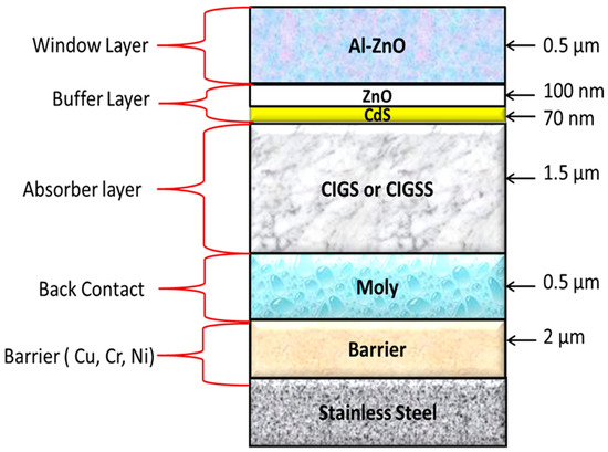
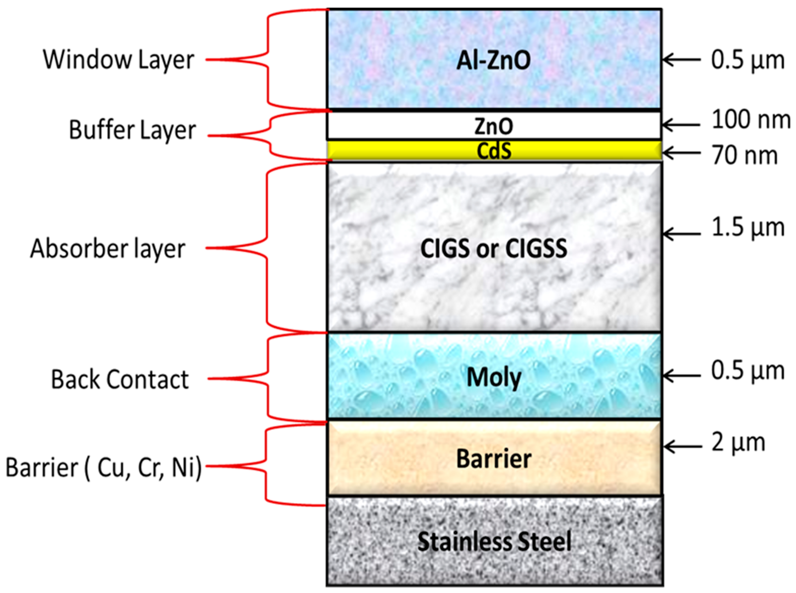
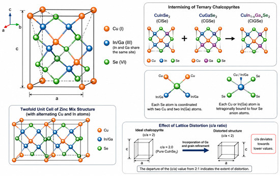
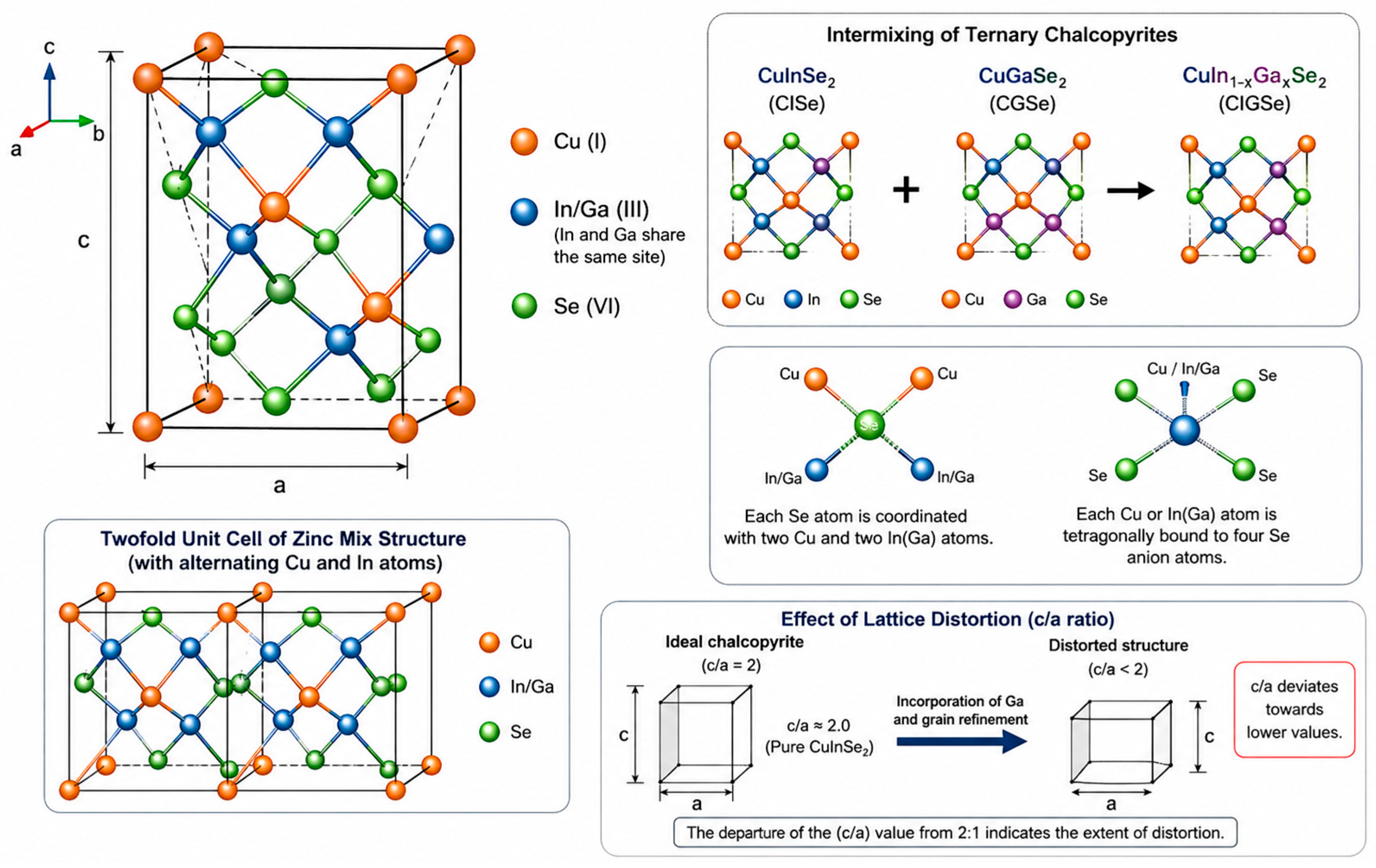
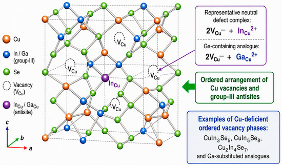
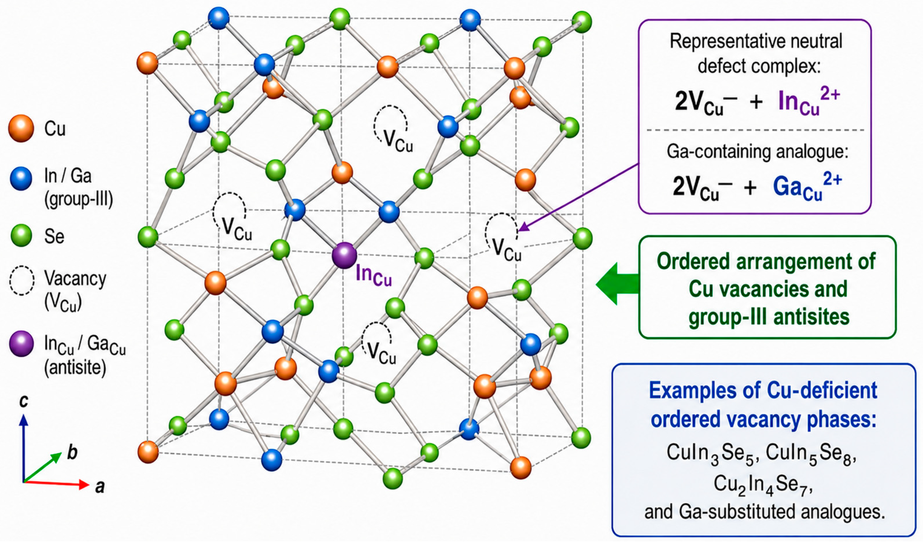
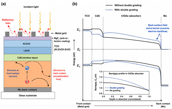
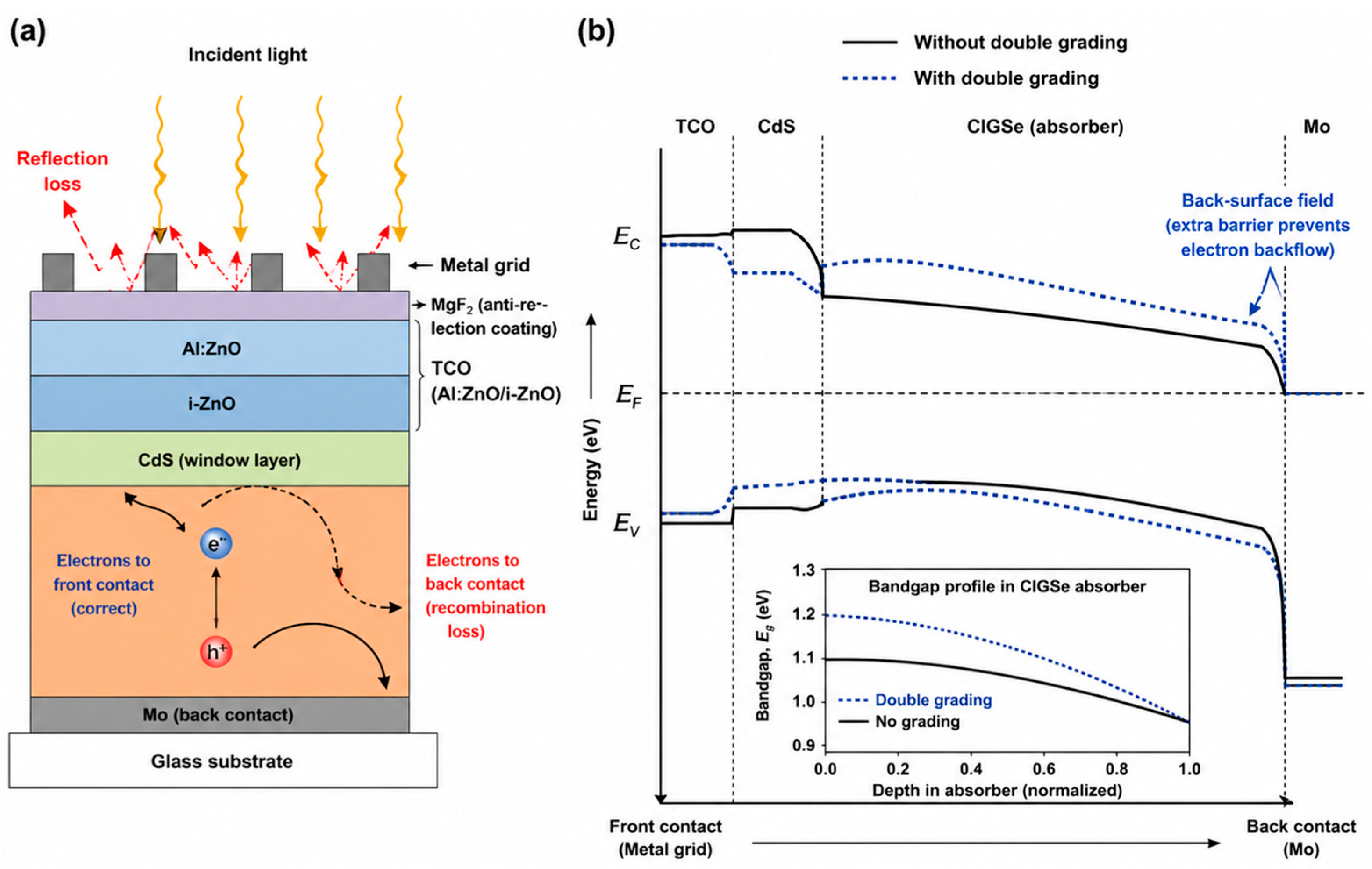
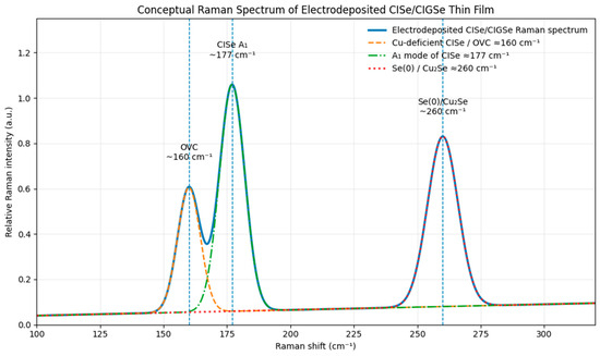
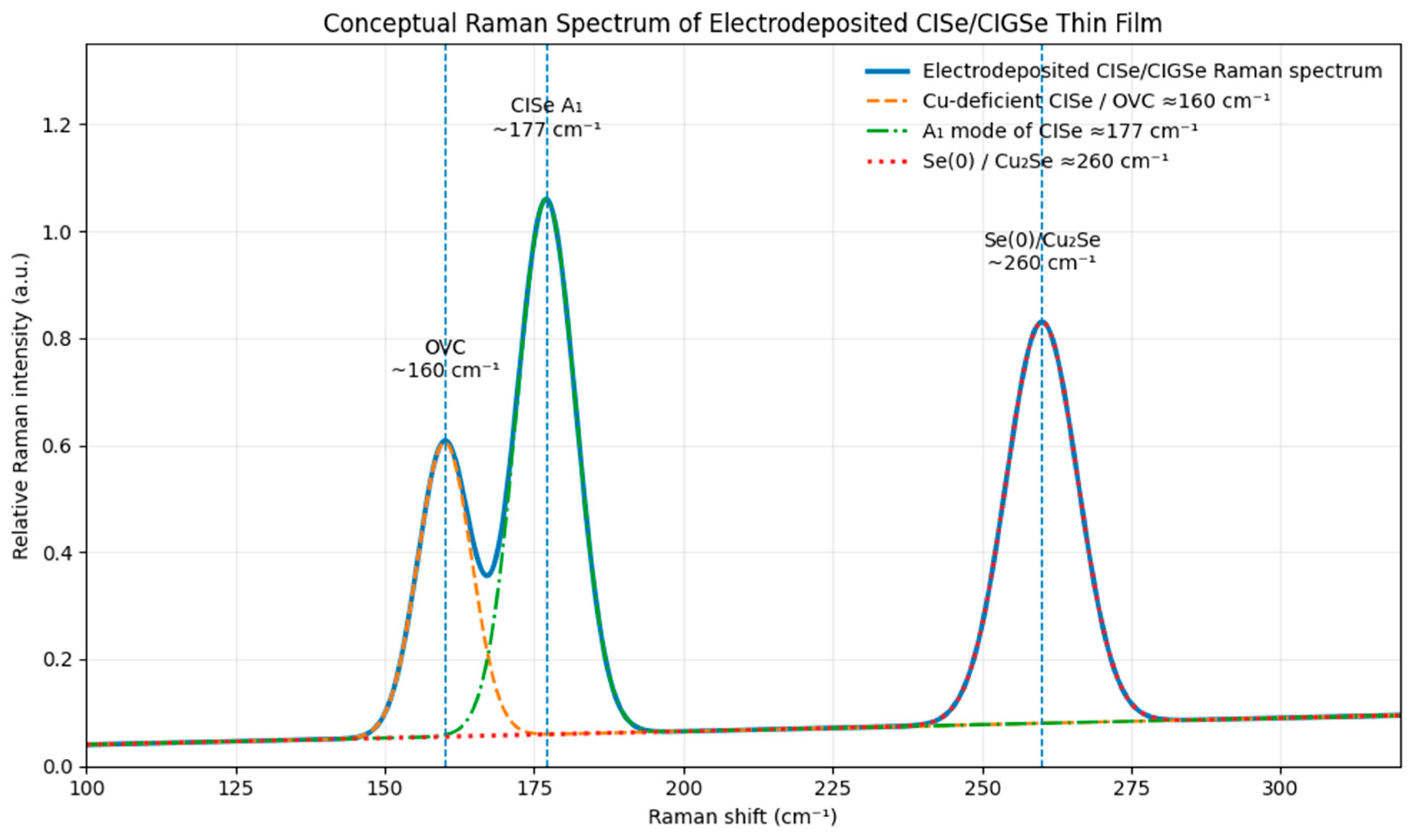
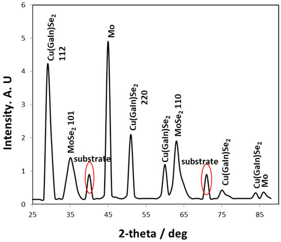
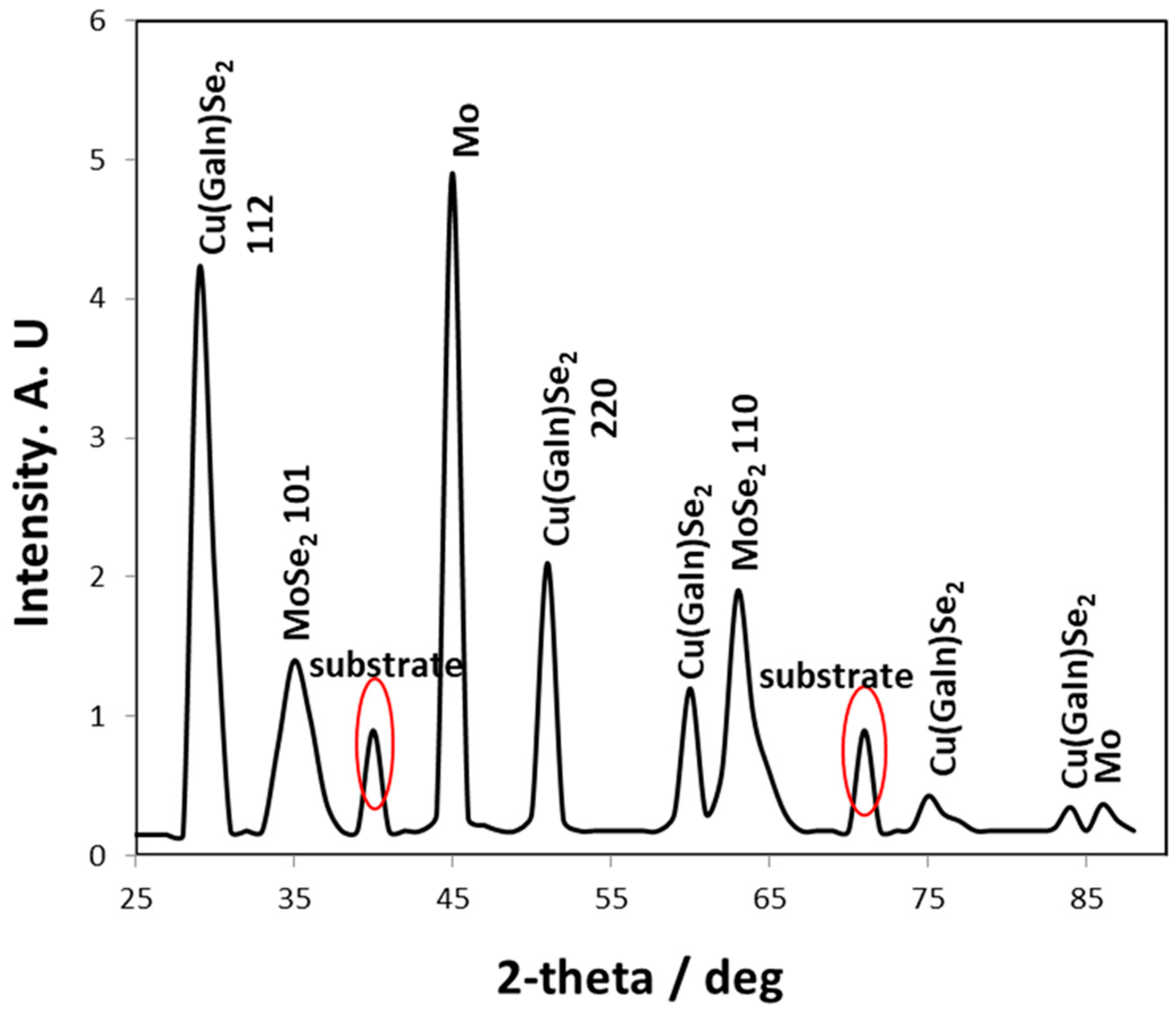
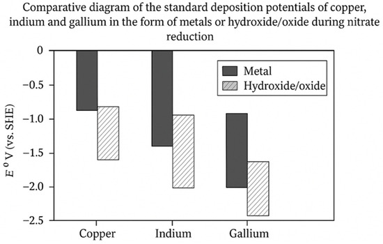
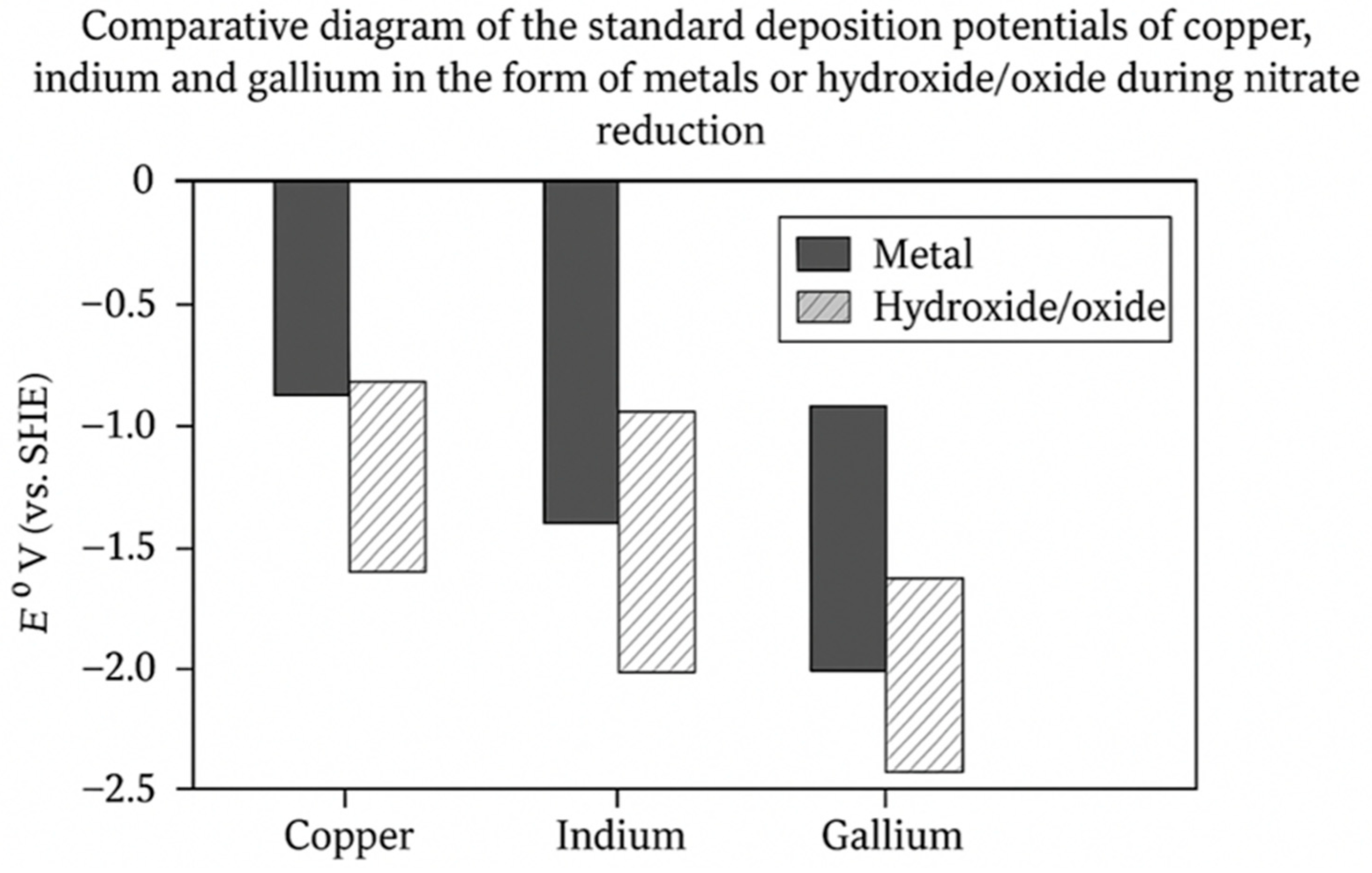
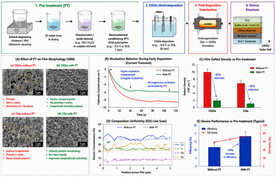
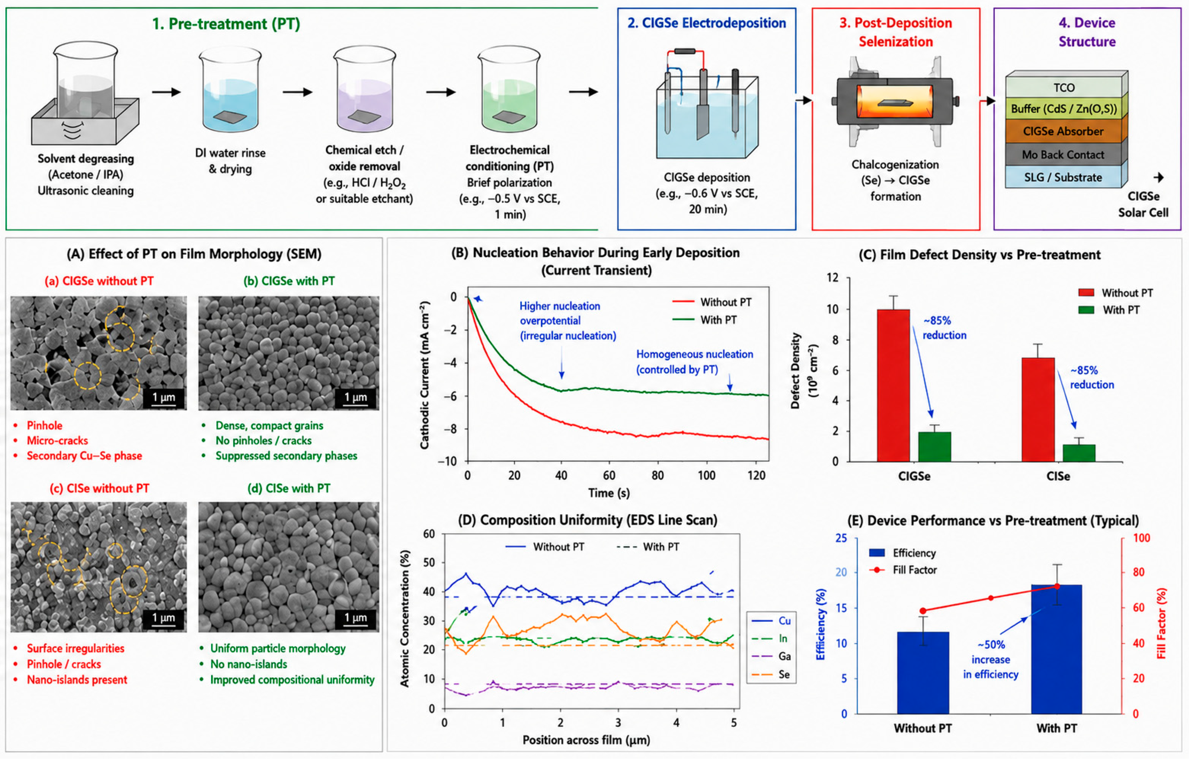
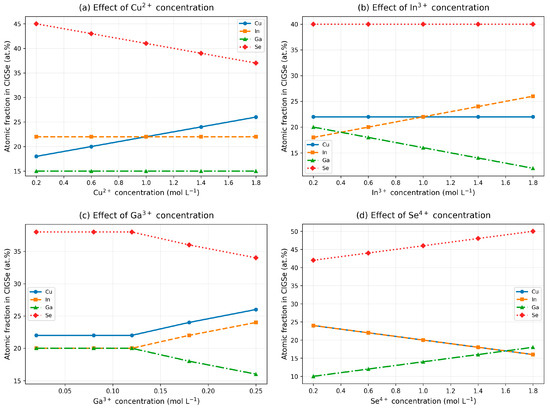
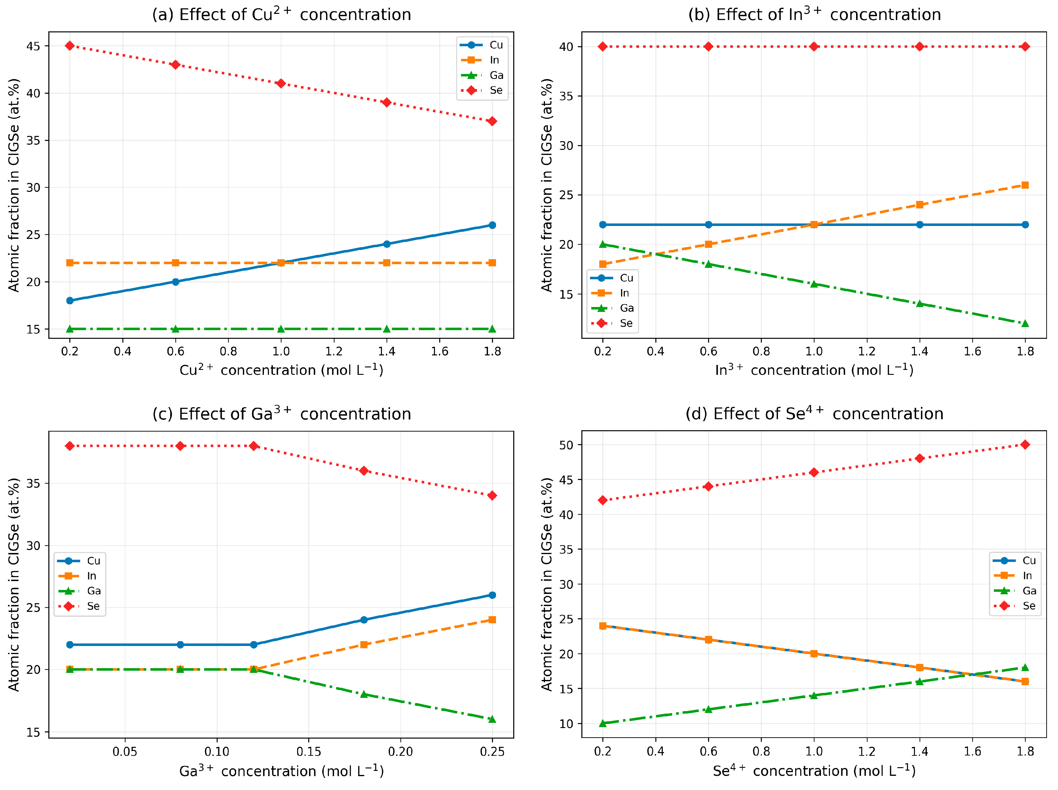
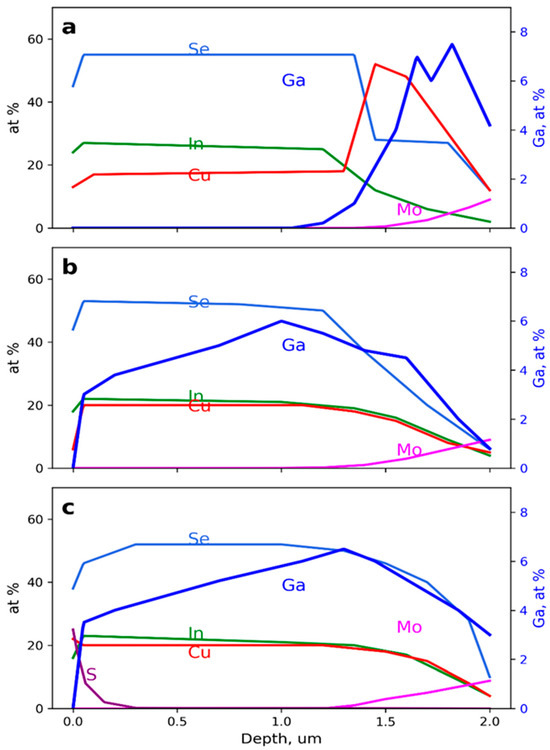
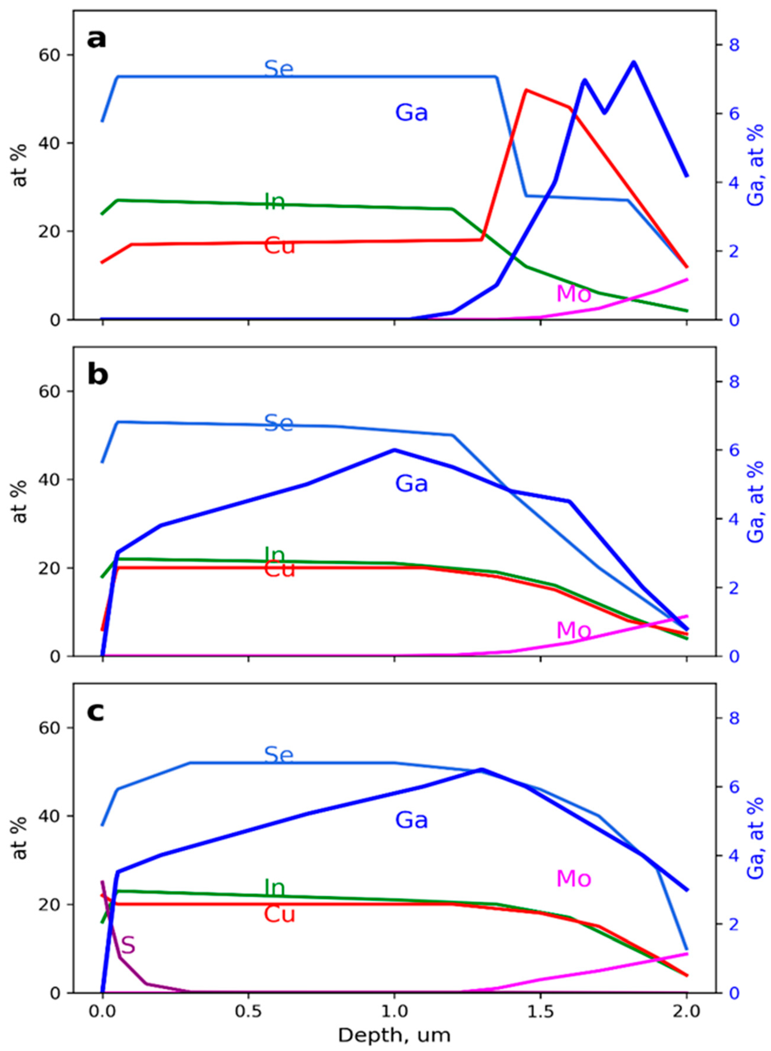
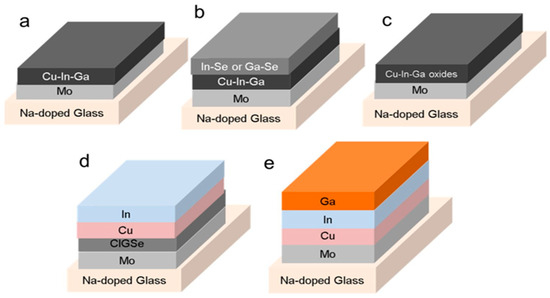
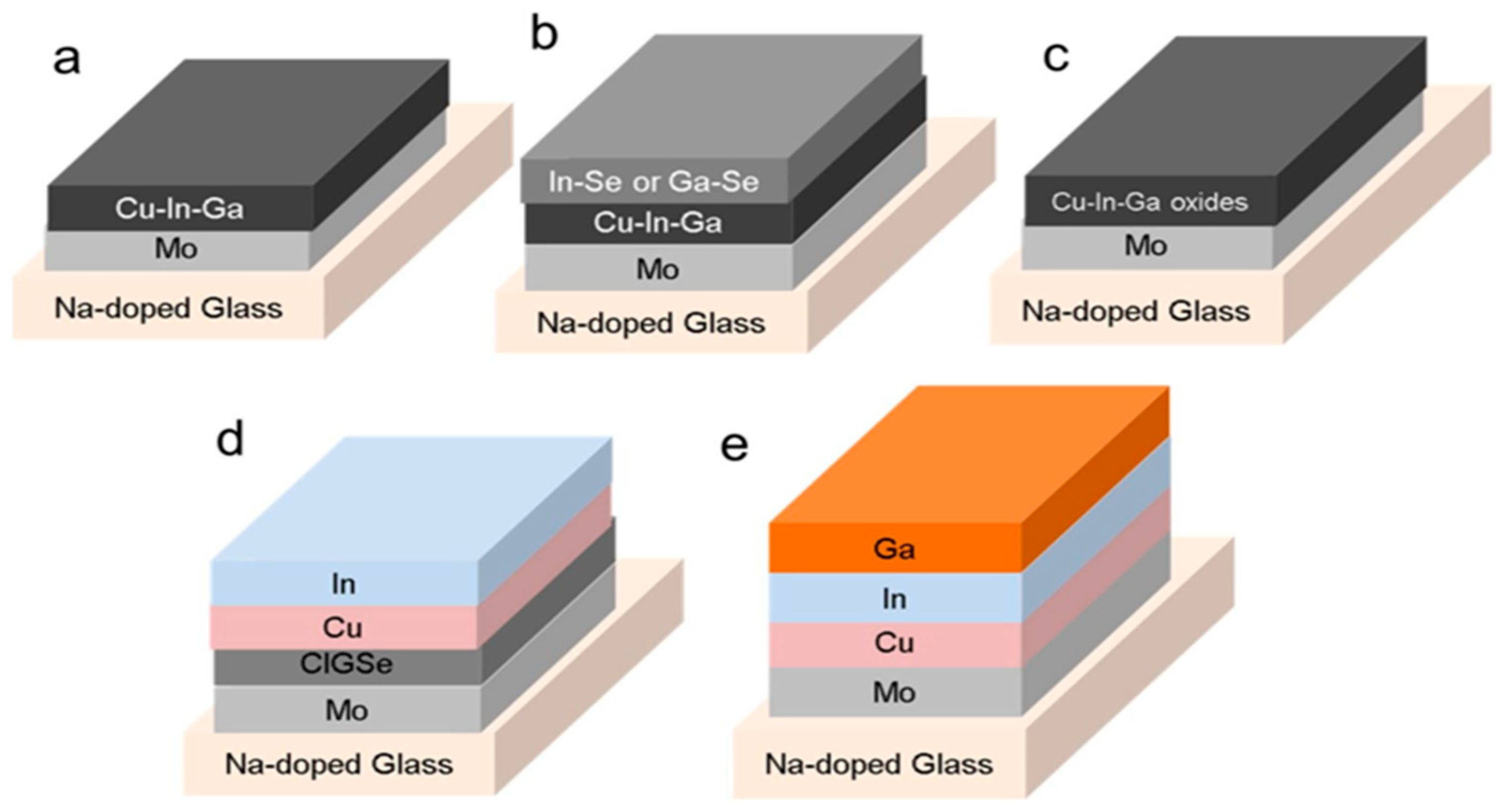
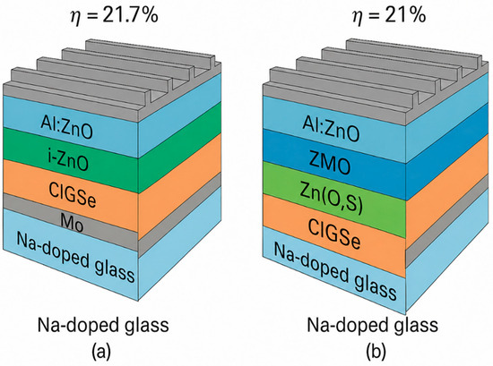
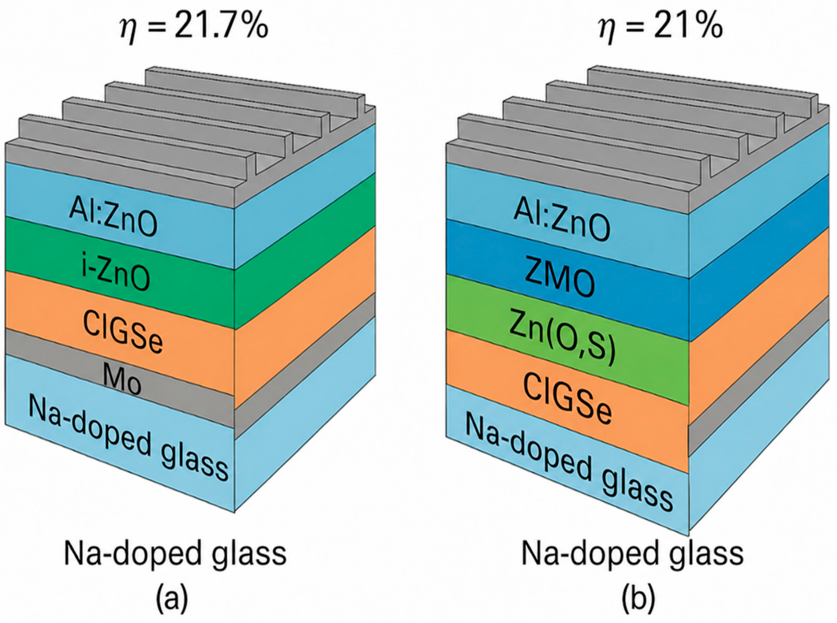

Disclaimer/Publisher’s Note: The statements, opinions and data contained in all publications are solely those of the individual author(s) and contributor(s) and not of MDPI and/or the editor(s). MDPI and/or the editor(s) disclaim responsibility for any injury to people or property resulting from any ideas, methods, instructions or products referred to in the content. |
© 2026 by the author. Licensee MDPI, Basel, Switzerland. This article is an open access article distributed under the terms and conditions of the Creative Commons Attribution (CC BY) license.