


Abstract
In the post-Moore era, large-area manufacturing of high-quality two-dimensional (2D) materials remains a central bottleneck for the industrialization of next-generation microelectronic and optoelectronic devices. Conventional mechanical exfoliation is limited by randomness and small lateral size, whereas chemical vapor deposition inevitably introduces grain boundaries, stress, and interfacial contamination, making it difficult to achieve both high quality and scalability. Metal-assisted exfoliation (MAE) enables controllable exfoliation and nondestructive transfer of large-area, high-quality monolayer 2D materials via precise modulation of metal-2D interfacial interactions dominated by strain-induced decoupling and atomic intercalation. This article systematically outlines the interfacial physical mechanisms and technological evolution of MAE, and highlights its state-of-the-art applications in patterned transfer, high-performance field-effect transistors, and complementary logic circuits, aiming to provide a firm theoretical and technical basis for advancing 2D materials from fundamental research toward practical applications.
1. Introduction
With semiconductor manufacturing [1] entering the atomic scale, the dimensional scaling of conventional silicon-based integrated circuits is approaching its physical limit, posing severe challenges to the continuation of Moore’s Law [2]. The search for new materials and systems to break through this bottleneck has become one of the most cutting-edge research directions in modern condensed matter physics and materials science. Two-dimensional (2D) layered materials [3,4,5,6,7,8], represented by graphene [9,10,11,12], transition metal dichalcogenides (TMDCs) [13,14,15], and hexagonal boron nitride (h-BN) [16,17,18,19] exhibit great application potential in nanoelectronics, optoelectronics, and quantum information by virtue of the quantum confinement effect [20,21] and unique band structure induced by their atomic-level thickness.
However, the properties of 2D materials [22,23,24] are closely related to their layer thickness, crystal quality, and interface cleanliness. Minor defects [25,26], doping [27], or contamination can lead to significant degradation in performance. For instance, monolayer MoS2 [28,29,30,31] undergoes an indirect-to-direct bandgap transition compared with its bulk counterpart, accompanied by greatly enhanced optical absorption coefficient and photoluminescence (PL) quantum yield, endowing it with prominent advantages in optoelectronic device [32]. Although the fundamental physical properties of 2D materials have been widely verified, translating these laboratory-scale materials into industrially applicable and stably performing engineering materials remains a formidable challenge. Therefore, achieving atomic-precision layer-number control, large-area low-defect exfoliation, and clean transfer constitutes a critical technical hurdle that must be overcome for 2D materials to advance from lab research to industrial applications.
Traditional preparation strategies for 2D materials suffer from an inherent trade-off between quality and scalability. The scotch-tape mechanical exfoliation method [33], which pioneered early 2D material research, can produce high-quality crystalline monolayers but suffers from low yield, random flake size, uncontrollable layer numbers, and potential adhesive residues, making it unsuitable for large-scale industrial production. In contrast, liquid-phase exfoliation [11,34,35,36] and chemical vapor deposition (CVD) [37,38,39,40] offer scalability but have distinct drawbacks. The former often causes severe degradation of carrier mobility due to solvent residues and structural defects; the latter, despite enabling large-area film growth, inevitably introduces grain boundaries, defects, and residual stress. Moreover, subsequent transfer processes readily generate wrinkles, cracks, and interface residues, severely restricting the intrinsic properties of materials and the uniformity of devices, thus failing to meet the requirements of high-end electronic and optoelectronic applications.
In the field of 2D material fabrication, achieving a balance between high quality and large-area scalability has long been a thorny challenge. Against this backdrop, metal-assisted exfoliation (MAE) [41,42,43,44,45] has emerged as a promising solution. The core physical essence of this technique lies in the precise regulation of interfacial interactions between metals and 2D materials to overcome interlayer van der Waals forces, thereby realizing the controllable preparation of large-area, intrinsically crystalline, and low-damage 2D materials.
In early explorations, noble metals represented by gold were extensively investigated to establish the feasibility of this approach. Specifically, Magda et al. [46] first demonstrated the successful exfoliation of large-area transition metal chalcogenide single layers using gold substrates, while Desai et al. [47] achieved ultra-large optoelectronically perfect monolayers by leveraging the strong chemical affinity between gold and chalcogen atoms. These pioneering works not only validated the feasibility of MAE but also provided a critical theoretical and experimental foundation for subsequent research.
Building upon these early achievements, the technique has been gradually extended to low-cost MAE systems represented by silver [44,45,48]. In addition, liquid metals (Ga) [49,50,51,52,53] with unique fluidity can also be used to exfoliate 2D materials, providing a new route for their isolation [54]. Studies have revealed that the mechanism of MAE is not determined solely by the adhesion strength at the metal-2D material interface, but is governed by multiple factors including interfacial strain distribution, energy dissipation pathways, and fine-tuning of interatomic interactions [43].
Based on the perspective of condensed matter physics, this paper establishes a comprehensive framework spanning from microscopic mechanisms to macroscopic applications. The core physical mechanisms of MAE are systematically analyzed, with a particular emphasis on strain-induced decoupling effects exemplified by gold. Subsequently, the applicable logic and technical advantages across diverse metal systems are revealed. Finally, the paper summarizes state-of-the-art progress in device integration, leveraging the high-quality, large-area advantages of this technique, including patterned transfer [55,56,57], high-performance field-effect transistors (FETs) [58,59,60,61], and complementary logic circuits [59,62,63]. By reviewing the physical mechanisms and technological evolution of MAE, this paper aims to provide theoretical insights into interfacial interactions in 2D materials and offer clear guidance on addressing key challenges such as large-area fabrication, interface cleanliness, and cost control, thereby facilitating the transition of 2D materials from laboratory research to large-scale industrial applications in the post-Moore era.
2. Physical Mechanisms of MAE
Compared to the limitations of traditional preparation methods for 2D materials in terms of scalability and controllability, MAE demonstrates significant application advantages. As summarized in Table 1, MAE demonstrates superior performance in maintaining atomically clean interfaces and high crystal quality, significantly outperforming traditional CVD transfer and liquid-phase exfoliation techniques. Although currently challenged by high precious metal costs and difficulties in continuous production, its unique advantages in fabricating high-performance electronic devices and complex van der Waals heterostructures [64,65,66,67,68] position MAE as a critical bridge connecting laboratory-based fundamental research with future large-scale manufacturing. However, to achieve precise control over this technology, merely optimizing the fabrication process is insufficient; it is essential to delve into the microscopic physical mechanisms. This section will systematically explain the core physical principles of MAE, laying a theoretical foundation for understanding the selection of different metal systems and future process development.
Table 1.
Comprehensive comparison of mainstream techniques for the preparation and transfer of 2D materials.
According to the thermodynamic theory of mechanical exfoliation [69], the physical essence of MAE lies in regulating the competitive relationship between the metal-2D material interfacial binding energy () and the interlayer binding energy of the 2D material (), which is generally expressed as
Theoretically, exfoliation occurs when [47]. For typical van der Waals materials [61,70,71,72] such as graphene and MoS2, the interlayer binding energy is approximately 20 meV/Å2 [73]. The interfacial binding energy depends on the metal type: inert metals (Au, Ag, Cu) interact with 2D materials mainly via van der Waals forces, with low binding energies and large interfacial distances, preserving the intrinsic electronic structure. In contrast, Ni, Pd, and other transition metals [74,75,76,77] show much stronger chemical affinity and form significantly higher interfacial binding energies [78].
Since gold-assisted exfoliation (GAE) stands as the most important and widely employed approach in MAE, it serves as the primary model system for analyzing the physical mechanism of MAE. This prominence is underscored by pioneering studies from Magda et al. [46] and Desai et al. [47], who demonstrated its efficacy in the fabrication of large-area, high-quality transition metal chalcogenides. Although the strong van der Waals interaction between gold and 2D materials serves as the core driving force for exfoliation, Ziewer et al. identified the core mechanism as strain-induced decoupling [43]. As highlighted by Ziewer et al., the advantage of Au originates not from conventionally perceived “strong adhesion” but from the unique interfacial strain at the Au substrate. High-frequency Raman characterization of MoS2 on Au provides critical experimental evidence: the mode of 2–4 layer MoS2 splits into a low-frequency peak, denoted as E(L), near 380 cm−1 and a high-frequency peak. According to Velický et al., while the splitting of the mode in this system is typically driven by charge doping, the splitting of the mode is attributed to the strain-induced lattice distortion [79]. This phenomenon indicates that, upon contact between MoS2 and Au(111), the bottommost MoS2 layer undergoes significant lattice distortion due to the interaction with the gold surface, while upper layers remain nearly unaffected. Furthermore, as demonstrated by Rodríguez et al., the strong interaction with the Au(111) surface induces symmetry breaking (reducing the symmetry from D3h to C3v), which activates specific Raman modes that are otherwise forbidden in freestanding monolayers [80]. Such strain localization directly weakens interlayer coupling.
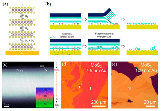
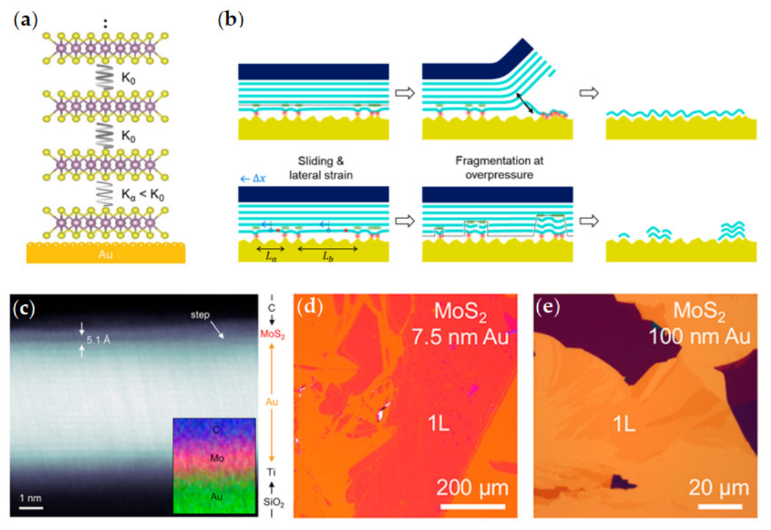
These studies indicate that cleavage occurs at the first interface of MoS2 crystals. To more intuitively illustrate the exfoliation mechanism, Ziewer et al. improved the linear chain model (LCM), as shown in Figure 1a, to describe the S1 mode of MoS2 on Au. Quantitative analysis of interlayer force constants () based on ultra-low-frequency Raman and the LCM reveals that the interaction strength between the first and second layers decays sharply with increasing total crystal thickness. For bilayers, is about 80% of (the force constant between other layers in pristine MoS2); for crystals thicker than five layers, approaches zero. This means that in thick crystals, the strained bottom layer becomes nearly fully decoupled from the upper lattice, turning this interface into the weakest cleavage plane and guiding preferential fracture for monolayer exfoliation. This conclusion is also supported by first-principles calculations [73]. The exfoliation energy turns negative when the biaxial strain induced by the substrate exceeds a threshold (≈3.5%) and the crystal thickness exceeds five layers, proving that efficient exfoliation can be achieved via strain-induced interlayer decoupling without requiring extremely strong interfacial adhesion.
Figure 1.
(a) Schematic illustration of the modified linear chain model (mLCM) [43]. Copyright by 2025, Jakob Ziewer et al. Advanced Materials published by Wiley-VCH GmbH. (b) Schematic of the pressure-controlled interface and the exfoliation process [81]. Copyright by 2024, Sikai Chen et al. Licensee MDPI, Basel, Switzerland. (c) HAADF-STEM image of monolayer MoS2 on 5 nm Au [41]. Copyright by 2018 American Chemical Society. Reproduced with permission. (d,e) Optical micrographs of MoS2 exfoliated on 7.5 nm and 100 nm Au, respectively [41]. Copyright by 2018 American Chemical Society. Reproduced with permission.
In addition, externally applied pressure plays a crucial role during the exfoliation process [81]. As illustrated in Figure 1b, appropriate pressure improves interfacial contact, optimizes strain distribution, and expands the effective area of the decoupled region. Precise pressure control to optimize strain distribution while avoiding lattice damage is a prerequisite for the exfoliation of large-area monolayer materials, providing new guidance for the development of efficient and controllable 2D material preparation technologies. However, the successful exfoliation on gold is also related to the cleanliness and roughness of the gold surface. Fresher and smoother gold surfaces yield better exfoliation effects.
So, how can it be proven that MoS2 and Au are bonded via van der Waals forces rather than stronger chemical covalent bonds. The experiments by Velický et al. provide the answer. They observed a clear MoS2/Au interface through the high-angle annular dark-field (HAADF)-STEM image in Figure 1c and measured the average distance between the center of the Mo atomic layer and the Au atomic center to be 5.1 ± 0.3 Å. Based on this distance, the spacing between the S atomic layer and the Au surface is derived to be approximately 3.5 Å. Since the typical Au-S covalent bond length is approximately 2.2 Å, it can be determined that the interaction between MoS2 and Au is a strong van der Waals interaction.
The aforementioned studies indicate that two core conditions must be met for successful GAE of 2D materials: first, the formation of good interfacial contact between the gold and the 2D material, and second, the application of appropriate external pressure. However, achieving large-area, high-quality monolayer exfoliation depends not only on the thickness and surface roughness of the gold film but is also closely related to the freshness of the gold film when exposed to air. The smoother and cleaner the gold film, and the shorter the exposure time after preparation, the better the exfoliation result. As clearly observed in Figure 1d,e, a 7.5 nm thick gold film yields better exfoliation results than a 100 nm thick film. Thicker gold films possess rougher surfaces, which weaken the van der Waals forces between the gold and MoS2. Experiments summarize that thin gold films with a thickness of 5–20 nm are most suitable for exfoliation. Furthermore, freshly prepared gold films must be used, as surface aging of the gold film rapidly weakens its van der Waals interaction with the material.
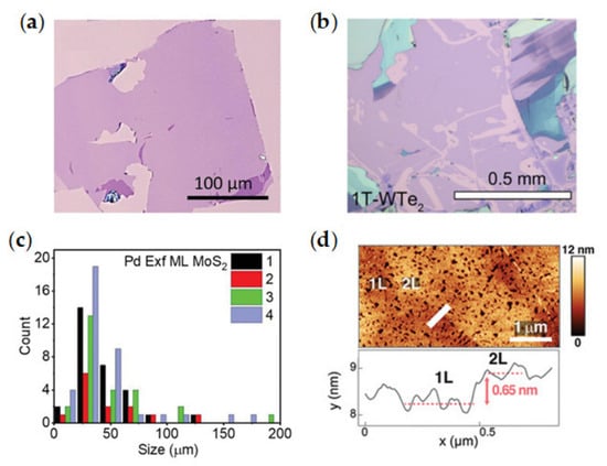
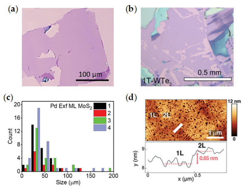
Early studies indicated that metals such as Pd, Cu, Ni, Ag, Al, and Mo often induced tearing or phase transitions during exfoliation due to excessive adhesion to the material. However, subsequent research by Johnston et al. revealed that this damage was primarily attributed to surface oxidation, which reduced interfacial binding energy and led to inhomogeneous exfoliation. It has been demonstrated that under ideal conditions of high-vacuum in situ deposition and an oxygen-free environment, metals like Pd, Cu, Ni, and Ag can still yield large-area, high-quality, and structurally intact MoS2 monolayers, with no observable phase transitions or structural damage, by virtue of their strong interfacial binding energy [82]. The optical microscopy image in Figure 2a intuitively displays the efficacy of Pd-assisted exfoliation of MoS2. Similarly, experiments by Fu et al. confirmed the capability of Ag in exfoliating large-area 2D materials; Figure 2b presents an optical image of Ag-exfoliated 1T-WTe2. Comparative analysis suggests that Ag exhibits the most superior exfoliation performance among these metals, comparable to that of Au. Furthermore, histograms of the lateral size distribution of MoS2 flakes obtained via Pd, Cu, and Ni assistance further corroborate the high reproducibility of this method, with the size distribution for Pd-exfoliated samples shown in Figure 2c. The atomic force microscopy (AFM) image in Figure 2d clearly depicts the edge morphology of Ag-exfoliated 1L–2L MoS2 flakes. The measured step height is approximately 0.65 nm, which aligns closely with the theoretical interlayer spacing of MoS2 [83].
Figure 2.
Optical microscope images of ML MoS2 exfoliated via (a) Pd-mediated routes [82]. Copyright by 2022 Wiley-VCH GmbH. Reproduced with permission. (b) Optical microscope image of 1T-WTe2 exfoliated on a 15 nm Ag film [44]. Copyright by 2022 Qiang Fu et al. Advanced Science published by Wiley-VCH GmbH. Yield statistics for (c) four Pd-mediated exfoliation processes [82]. Copyright by 2022 Wiley-VCH GmbH. Reproduced with permission. (d) AFM image of the 1L-2L edge region [48]. Copyright by 2022 Max Heyl et al. Advanced Materials Interfaces published by Wiley-VCH GmbH.
In summary, interfacial binding energy serves as the necessary thermodynamic condition for MAE, determining the fundamental feasibility of the process. For metals such as Pd, Cu, Ni, and Ag, efficient exfoliation can be achieved under oxidation-free in situ conditions driven primarily by their high binding energies. However, for Au-assisted exfoliation, adhesion alone is insufficient to guarantee high-quality, large-area monolayer cleavage. Strain-induced decoupling acts as the key mechanism enabling this superior performance. Binding energy and strain regulation function synergistically rather than independently to govern exfoliation outcomes. Although a binding energy exceeding the interlayer van der Waals forces is essential for all systems, Au distinguishes itself by inducing localized interfacial strain through strong interactions. This strain localization further weakens interlayer coupling and enhances the uniformity of the exfoliated layers.
3. Selection of Metal Types
Since the emergence of graphene in 2004, the mechanical exfoliation method (Scotch Tape Method) has rapidly become a classic approach for early explorations of the intrinsic physical properties of 2D materials [9]. It features simple operation, low equipment requirements, no need for complex experimental setups, and enables rapid acquisition of monolayer 2D materials. This method uses transparent scotch tape to repeatedly exfoliate high-quality monolayer materials. However, it suffers from inherent drawbacks including low yield, small flake size, high randomness, and high contamination risk, which restrict its application scenarios and make it difficult to meet the strict requirements of high-performance electronic devices for interface cleanliness and process integration.
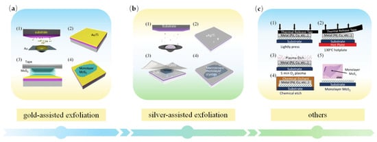
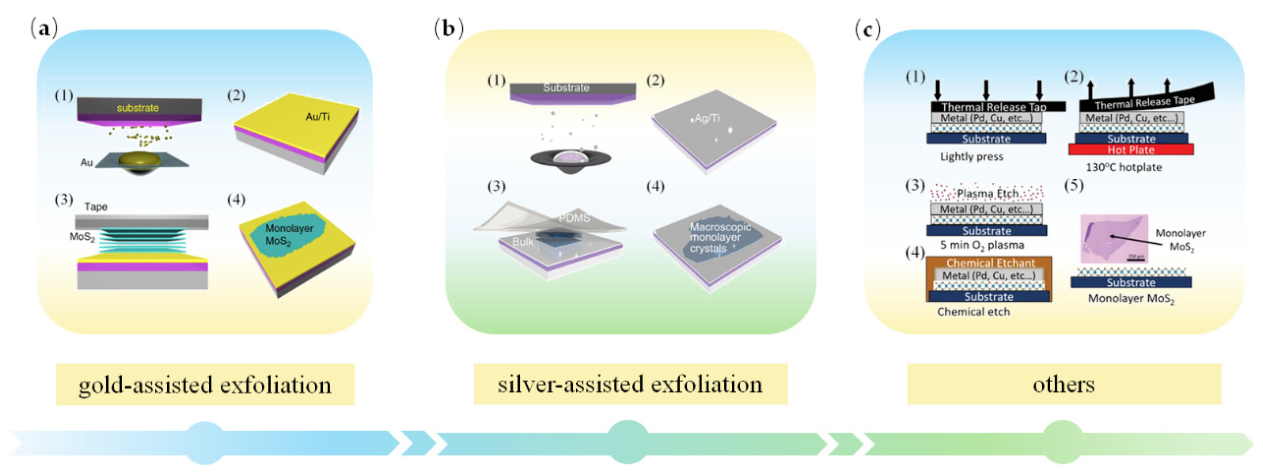
Huang et al. proposed a universal GAE technique [42]. As shown in Figure 3a, an adhesion layer (Ti/Cr) and a gold layer are evaporated onto substrates (e.g., Si/SiO2, quartz, flexible plastics). Subsequently, bulk crystals are then pressed onto the Au film under slight pressure and held for 1–5min, followed by slow peeling, which can yield large-area monolayer regions under optimized conditions on the Au surface. This method is not only applicable to common TMDCs (e.g., MoS2) but has also successfully exfoliated 40 different types of 2D materials, including black phosphorus (BP) [7,68,84,85,86,87], magnetic materials [88,89,90] such as Fe3GeTe2 [91,92] and CrCl3 [93,94], superconductors [95] like FeSe [96,97] and NbS2 [98,99], as well as difficult-to-exfoliate materials such as RuCl3 [100,101] and PtTe2 [102]. The as-obtained monolayer crystals can reach millimeter-scale to even centimeter-scale sizes, which are far beyond the micrometer-scale fragments obtained by the traditional tape method, although the exfoliation is limited by the size of the bulk crystal itself. Furthermore, no subsequent polymer transfer [103,104] (e.g., PMMA) is required, avoiding residual contamination. By tuning the thickness of the Au film, high-performance electronic devices (e.g., FETs) can be directly fabricated on the Au film, and the materials can be easily transferred onto arbitrary substrates.
Figure 3.
Schematic illustration of the MAE process for different metals: (a) Gold-assisted exfoliation [42]. Copyright by 2020 Yuan Huang et al. (b) Silver-assisted exfoliation [44]. Copyright by 2022 Qiang Fu et al. Advanced Science published by Wiley-VCH GmbH. (c) Exfoliation assisted by other transition metals [82]. Copyright by 2022 Wiley-VCH GmbH. Reproduced with permission.
Although the GAE method enables the fabrication of large-area, high-quality 2D monolayers, it still has two major drawbacks in practical applications. First, the high cost of gold limits its scalability for industrial applications. Second, the direct contact between the Au film and 2D semiconductors significantly quenches PL, thereby restricting the investigation of optical properties [44]. To address these issues, Fu et al. proposed using Ag as an alternative metal. The exfoliation process is analogous to the gold-assisted method, as illustrated in Figure 3b. The monolayer dimensions are comparable to those obtained via gold-assisted methods, demonstrating the excellent large-area exfoliation capability of silver films. Furthermore, theoretical calculations confirm that the interaction between silver and 2D materials minimally perturbs the electronic band structure, thus preserving the intrinsic electronic properties of the materials. Compared to gold, silver is not only more cost-effective but also exhibits distinct surface morphological characteristics. Thermally evaporated Ag films possess a highly rough surface composed of aggregated nanoparticles. This unique roughness excites plasmons, which, rather than quenching the PL of materials like MoS2, significantly enhances the signal. Characterization of the normalized PL intensity of monolayer MoS2 and MoSe2 on Ag films of varying thicknesses reveals that the materials on a 5 nm Ag film substrate exhibits the strongest PL signal. Additionally, a comparison of PL signals from MoS2 on smooth versus rough Ag films shows that while the former exhibits a typical metal-induced quenching effect, the latter displays an extremely strong A-exciton PL emission peak at approximately 1.86 eV, which has never been observed in other mechanical exfoliation techniques.
Although Au and Ag are excellent choices for high-quality exfoliation, given their high cost, it is necessary to explore more abundant alternatives. In order to further broaden the scope of metal choices for MAE, researchers have explored cost-effective alternative metals such as Pd, Cu, and Ni. The exfoliation processes of MoS2 assisted by these metals are illustrated in Figure 3c. Although these metals may not induce the same degree of strain engineering [105,106] effects as gold, they exhibit sufficiently high interfacial binding energies to facilitate efficient exfoliation. As shown in the previous section, Pd, Cu, Ni, and Ag can all obtain high-quality monolayer MoS2 through oxidation-free in situ processes. This indicates that even without the significant plasmonic enhancement or strain decoupling mechanisms in gold or silver systems, it is sufficient to achieve the preparation of large-area, high-crystallinity 2D materials, thereby providing a more economically viable pathway for practical applications.
In addition, Bai et al. innovatively used Ga to intercalate and exfoliate various layered materials at near-room temperature [54]. Traditional methods for 2D material exfoliation such as liquid-phase exfoliation and electrochemical intercalation [107,108,109,110,111] suffer from contamination, extra defect introduction, small lateral product sizes, and poor universality. Gallium is in a molten state at near-room temperature, combining both fluidity and metallic properties. In the experiment, molten gallium and layered materials are mixed via magnetic stirring for 24 h. Ga atoms successfully intercalated into the MoS2 interlayers, significantly expanding the interlayer spacing from approximately 0.6 nm to approximately 1 nm and forming pocket-like structures approximately 1 nm in height and 8 nm in width. During this process, gallium naturally oxidizes to form Ga2O3, which has an adhesion energy higher than the interlayer van der Waals forces, providing shear force for exfoliation under gentle stirring. Furthermore, Raman, X-ray diffraction (XRD), and X-ray photoelectron spectroscopy (XPS) characterizations confirmed that MoS2 and WS2 [112] underwent a 2H to 1T’ phase transition after Ga intercalation, a property that holds significant application value in catalysis [113,114] and other fields.
Collectively, the evolution from the Scotch Tape method to advanced MAE strategies has not only stimulated enthusiasm for 2D material exploration but also provided a robust technological pathway for property investigation. While mechanical exfoliation laid the foundation, the continuous innovation in MAE, ranging from noble metals [115] to cost-effective alternatives and liquid metals, has addressed limitations in yield and size. This diversified metal system, with its coexisting and complementary advantages, empowers researchers to flexibly select the optimal strategy based on material characteristics and application demands, truly realizing the tunable and controllable synthesis of 2D materials.
4. Application Expansion of MAE Technology
MAE has evolved from a simple material preparation method into a key bridge connecting fundamental research on 2D materials with industrial applications. The core value of this technology lies in its ability to simultaneously achieve large-area fabrication and high-quality preservation of materials, providing an ideal platform for maximizing the intrinsic properties of 2D materials in scalable manufacturing processes. This unique advantage enables MAE not only to focus on preparing high-quality materials but also to promote their transition from microscopic laboratory exploration to macroscopic system-level integration. Based on the dual advantages of quality and area of the obtained 2D materials, the application prospects of MAE can be elaborated from the following two aspects.
4.1. High-Performance Devices Based on High-Quality Characteristics
Benefiting from the low lattice damage and high intrinsic crystallinity of 2D materials obtained through MAE, they exhibit excellent physical properties approaching theoretical limits. This material foundation makes it possible to explore the performance boundaries of micro-nanoelectronics, enabling researchers to construct high-performance transistors, high-sensitivity sensors, and novel quantum devices, thereby delving deeper into the application potential of 2D materials at extreme scales.
Although mechanical exfoliation produces high-quality 2D materials, its random nature and limited flake size severely hinder large-scale device integration. CVD enables scalable production but inevitably introduces structural defects that degrade carrier mobility. The emergence of GAE successfully overcomes these challenges and unlocks the fabrication of high-performance TMDC field-effect transistors.
Since the gold-tape exfoliation technique directly yields continuous monolayers from bulk single crystals [116], it completely circumvents the intrinsic grain boundaries and polycrystalline scattering centers associated with CVD growth. Consequently, carrier transport is able to approach the intrinsic phonon-limited regime.
Specifically, in the study by Olsen et al. [60], MoS2 FETs fabricated via the modified gold-tape exfoliation method exhibited a superior room-temperature field-effect mobility of 250 ± 20 cm2 V−1 s−1. This value is approximately 5 times higher than that of CVD-grown counterparts and aligns closely with the theoretical phonon-limited mobility, providing direct evidence of the material’s exceptional electrical quality.
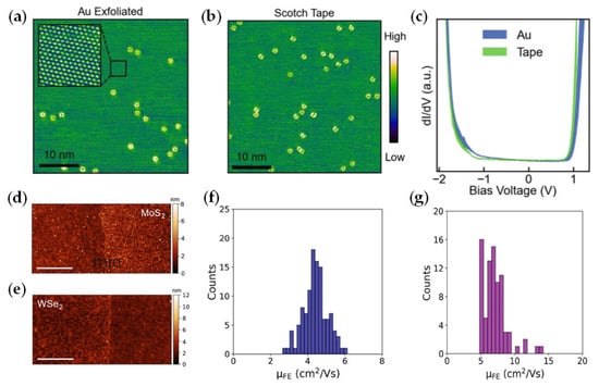
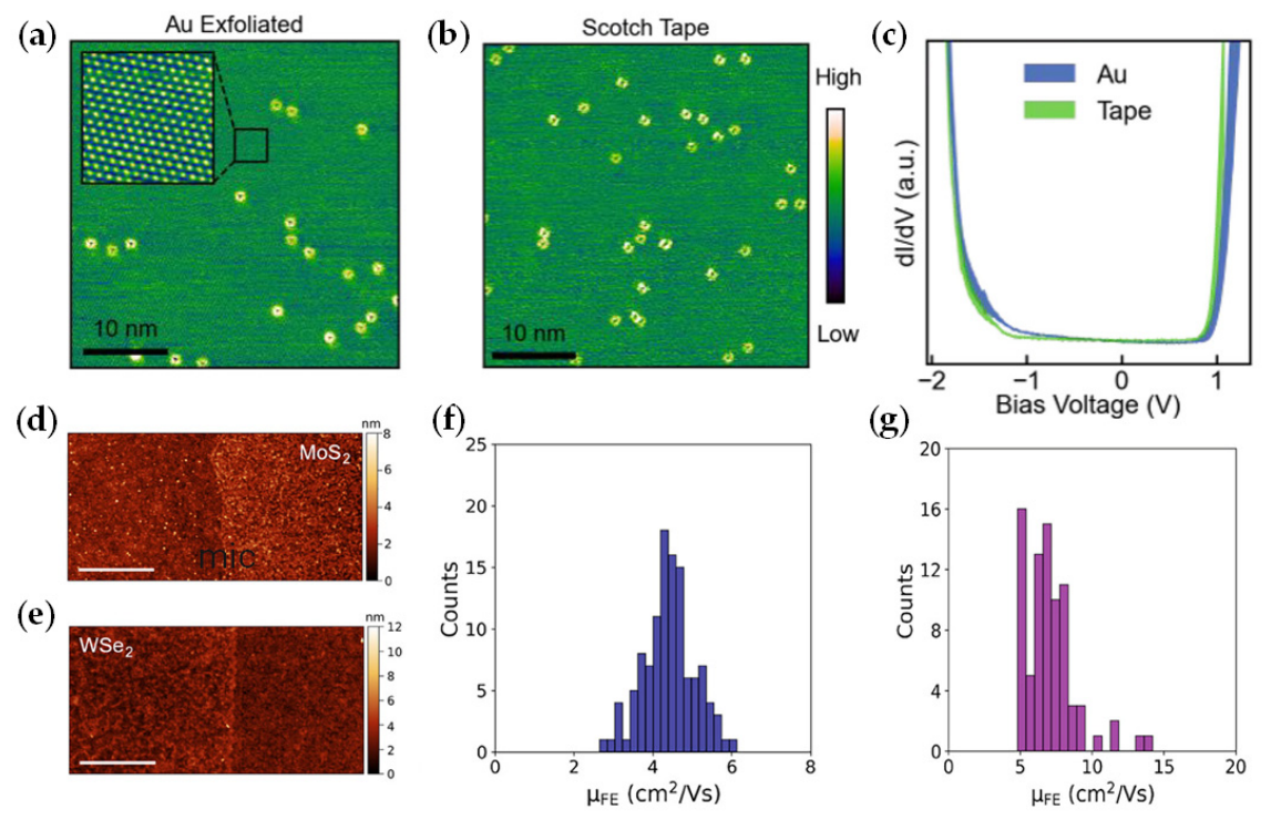
To elucidate the microscopic mechanism behind this high performance, Olsen et al. employed scanning tunneling microscopy (STM) and scanning tunneling spectroscopy (STS) for atomic-level characterization. As shown in Figure 4a, the surface of the gold-exfoliated WSe2 [117] monolayer is atomically clean. Notably, it presents equivalent point defects compared to the Scotch-tape exfoliated WSe2 monolayer from the same mother crystal (Figure 4b), indicating that the cleanliness of monolayers obtained by both methods is comparable, with no additional defects or doping introduced by the process. Furthermore, the STS band structure in Figure 4c reveals that its electronic structure is fully consistent with that of the intrinsic material. This further confirms that the high performance stems from the preservation of the material’s intrinsic electronic structure during the exfoliation process.
Figure 4.
(a) STM image of a monolayer WSe2 on graphite obtained by GAE; the inset displays atomic resolution [60]. Copyright by 2025 American Chemical Society. Reproduced with permission. (b) STM image of a monolayer WSe2 on graphite prepared using conventional Scotch tape exfoliation [60]. Copyright by 2025 American Chemical Society. Reproduced with permission. (c) Spatially averaged STS curves of monolayer WSe2 from gold-tape (blue) and Scotch-tape (green) exfoliation. Error bars correspond to standard deviations of 13 and 19 individual STS spectra, respectively [60]. Copyright by 2025 American Chemical Society. Reproduced with permission. (d,e) AFM images of (d) MoS2 and (e) WSe2 monolayers on SiO2/Si substrates [59]. Copyright by 2025 Małgorzata Giza et al. Small Methods published by Wiley-VCH GmbH. (f,g) Histograms showing the statistical distribution of field-effect mobilities for (f) MoS2 and (g) WSe2 devices [59]. Copyright by 2025 Małgorzata Giza et al. Small Methods published by Wiley-VCH GmbH.
Meanwhile, the study by Giza et al. validated the stability of this method on a macroscopic scale [59]. AFM characterization in Figure 4d,e demonstrates that gold-assisted exfoliated MoS2 and WSe2 monolayers possess atomically flat surface morphologies on SiO2/Si substrates. Based on device arrays constructed from these large-area monolayers (comprising over 100 devices), the field-effect mobility statistical histograms in Figure 4f,g exhibit an extremely narrow distribution.
Based on the high-quality structural and electronic characteristics established above, the fabricated FETs demonstrate exceptional performance, underscoring the method’s capability to realize the intrinsic potential of TMDCs in electronic applications.
4.2. System-Level Integration and Manufacturing Based on Large-Area Uniformity
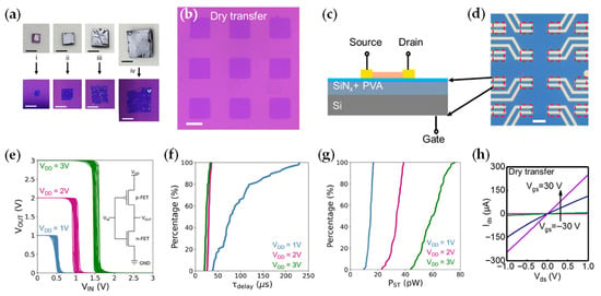
MAE technology has laid a solid foundation for the industrial application of 2D materials by virtue of its exceptional capability in large-area monolayer preparation. The exfoliation area is generally governed by the dimensions of the bulk crystal. Figure 5a presents optical images of four MoS2 bulk crystals with varying sizes and flatness, alongside the corresponding monolayers prepared from these bulk crystals on SiO2/Si substrates using the GAE method. This large-area monolayer provides an ideal material platform for constructing high-performance complementary metal-oxide-semiconductor (CMOS) circuits.
Figure 5.
(a) Optical images of MoS2 bulk crystals with varied sizes and flatness, and the corresponding monolayers obtained by GAE on SiO2/Si substrates [59]. Copyright by 2025 Małgorzata Giza et al. Small Methods published by Wiley-VCH GmbH. (b) Corresponding optical image of monolayer MoS2 arrays on a PVA-modified SiO2 substrate [118]. Copyright by 2021 American Chemical Society. Reproduced with permission. (c,d) Schematic illustration and optical micrograph of back-gated monolayer MoS2 transistor arrays [118]. Copyright by 2021 American Chemical Society. Reproduced with permission. (e) Output characteristics of 50 CMOS inverters measured at supply voltages VDD = 1, 2, and 3 V [59]. Copyright by 2025 Małgorzata Giza et al. Small Methods published by Wiley-VCH GmbH. (f,g) Cumulative distribution functions of (f) delay time and (g) static power at VDD = 1, 2, and 3 V [59]. Copyright by 2025 Małgorzata Giza et al. Small Methods published by Wiley-VCH GmbH. (h) Output and transfer characteristics of a dry-exfoliated monolayer MoS2 device, showing typical ohmic contact behavior [118]. Copyright by 2021 American Chemical Society. Reproduced with permission.
Building upon this, researchers have further developed lithography-based patterning techniques, upgrading MAE from a simple transfer tool into a precision manufacturing platform. By pre-designing the geometry of the gold templates, site-specific and shape-defined placement of 2D materials can be achieved. Consequently, this allows for the exfoliation of patterned monolayers as shown in Figure 5b and their direct integration into the complex circuit layouts depicted in Figure 5c,d, eliminating the need for subsequent etching processes and significantly reducing potential damage to the material lattice. This series of advances not only validates the feasibility of MAE technology in constructing complex electronic systems but also paves the way for its industrial applications in fields such as flexible electronics and large-scale integrated circuits.
The realization of high-performance CMOS serves as a critical benchmark for any 2D material synthesis technique. In the case of GAE, the production of large-scale, single-crystalline layers eliminates the grain boundary scattering that typically degrades carrier mobility in polycrystalline CVD films. This superior material quality enabled Giza et al. to fabricate balanced n-type and p-type FETs, which were subsequently integrated into CMOS inverters [59]. These inverters demonstrated clear logic inversion with a switching threshold near VDD/2 (Figure 5e), confirming the high quality and uniformity of the exfoliated layers. The devices further exhibited a minimum delay time of 20 μs (Figure 5f) and static power consumption as low as 44 pW (Figure 5g), demonstrating that GAE is a highly promising route for the scalable production of energy-efficient 2D electronic systems.
While patterning elevates GAE into a precise manufacturing platform, traditional Au-film exfoliation necessitates subsequent wet etching [119] using agents such as KI/I2 to remove the Au layer [42,120]. This process inevitably introduces oxidation, doping, interface residues, and lattice damage to the 2D materials, severely degrading their intrinsic properties and device performance. To address this, Li et al. developed a composite exfoliation tape composed of Au grids and polycarbonate (PC), which combines the strong van der Waals forces between metals and 2D materials with the superior support and flexibility of polymers [118]. This method not only enables the efficient exfoliation of large-area 2D monolayers but also allows for controllable release via the Au-free regions of the grid holes during subsequent transfer, thereby maximizing the preservation of the intrinsic properties of the 2D materials. Based on this, high-performance transistors were constructed. As shown in Figure 5h, detailed electrical characterization reveals that the output characteristics exhibit linear behavior, indicating the formation of good ohmic contacts [121] between the metal and the monolayer MoS2. Furthermore, both the drive current and carrier mobility reach excellent levels for monolayer MoS2 devices. This approach enables the optimization of material and device performance without requiring complex contact engineering or top-gate structures.
Beyond device fabrication, this precise control extends to the quantum realm. By enabling the precise definition and alignment of crystallographic orientations (such as straight step edges) on the template, this approach permits fine control over the twist angle of bilayer 2D materials. Such fine angular manipulation is critical for constructing Moiré superlattices [122,123], where minute variations in the twist angle induce drastic modifications to interlayer coupling and electronic band structures, leading to emergent physical phenomena such as flat bands and correlated electronic states. Studies have confirmed that Moiré superlattices fabricated via this method exhibit angular errors below 0.3°, providing an ideal platform for investigating correlated quantum states, including superconductivity and Mott insulating physics [55].
5. Summary and Outlook
This review systematically summarizes the latest advancements in MAE technology for preparing high-quality, large-area 2D materials. Addressing the bottlenecks of traditional mechanical exfoliation, such as low yield and small size, and those of CVD, including grain boundary defects and interface contamination, MAE achieves controllable exfoliation and non-destructive transfer of high-quality monolayer materials from centimeter to large scale by precisely modulating the interfacial interactions between metals and 2D materials.
From a mechanistic perspective, the MAE process is governed by a synergistic interplay between thermodynamics and mechanical regulation. While the interfacial binding energy dictates the thermodynamic feasibility of exfoliation, the strain-induced decoupling effect is pivotal in determining the quality of the cleavage. In the paradigmatic gold-assisted system, localized strain, which primarily arises from interfacial interactions and surface topography, effectively weakens interlayer coupling. This establishes the bottom monolayer as the preferential fracture plane, thereby enabling the acquisition of large-area, high-crystallinity monolayers. Looking ahead, the precise engineering of external stimuli, such as interfacial pressure, holds promise for optimizing strain distribution. This represents a critical pathway toward enhancing the uniformity and scalability of the exfoliation process.
Regarding technological evolution, MAE has expanded from its initial noble metal systems to include low-cost metals, Ga, and composite media systems. Silver-assisted exfoliation not only reduces costs but also utilizes its rough surface to activate plasmons, enhancing the optical properties of the materials. Liquid metal intercalation provides new pathways for exfoliating difficult-to-process materials and regulating phase transitions. Meanwhile, the emergence of dry exfoliation techniques effectively avoids oxidation and residue issues associated with wet etching, maximally preserving the intrinsic properties of the materials.
In terms of applications, MAE has become a cornerstone for constructing high-performance devices. Combined with lithographic patterning technologies, MAE enables site-specific, shape-defined transfer and precise control of twist angles, providing an ideal platform for researching Moiré superlattices and correlated quantum states. FETs fabricated using MAE exhibit carrier mobilities approaching intrinsic limits and extremely high on/off ratios. The successful integration of all-2D CMOS validates its immense potential for low-power electronic devices in the post-Moore era.
Although MAE technology has achieved significant breakthroughs in laboratory research, bridging the gap from fundamental research to large-scale industrial manufacturing requires addressing several interconnected challenges. Primarily, the high cost and discontinuous nature of gold films necessitate a shift toward low-cost transition metal alternatives like copper and nickel, alongside optimized recycling processes and the development of roll-to-roll technologies [45,124,125] to achieve environmentally friendly, large-scale production. Concurrently, achieving atomic-level precision in interface engineering is crucial; despite MAE’s ability to create clean interfaces, risks such as metal atom diffusion and oxidation persist, calling for in situ vacuum processing and novel buffer layers to enhance device stability and consistency. Beyond scaling, the superior interface compatibility of MAE offers a unique opportunity to construct complex van der Waals heterostructures—integrating superconducting devices. Furthermore, to fully realize the potential of 2D materials in optoelectronics [126], future research needs to synergistically optimize optical and electronic properties by mitigating fluorescence quenching through advanced substrates like silver nanostructures, thereby ensuring simultaneous improvements in carrier transport and photoelectric response for next-generation high-performance devices.
In conclusion, as a bridge connecting fundamental physics research of 2D materials with industrial applications, MAE technology occupies a core position in micro-nano electronic manufacturing in the post-Moore era due to its unique advantages. With deepening understanding of the underlying mechanisms and continuous innovation in process technologies, MAE is poised to thoroughly resolve the challenges of scalable preparation of 2D materials, accelerating the industrial-scale integration of next-generation integrated circuits and optoelectronic devices.
Author Contributions
Conceptualization, M.W.; writing—original draft preparation, M.W.; writing—review and editing, Z.H., Y.C. and X.Q.; visualization, M.W.; supervision, Z.H., Y.C. and X.Q.; funding acquisition, Z.H. and X.Q. All authors have read and agreed to the published version of the manuscript.
Funding
This work is supported by the Grants from National Natural Science Foundation of China (Nos. 12304091), Natural Science Foundation of Hunan Province of China (No. 2025JJ50054).
Data Availability Statement
Data sharing is not applicable.
Conflicts of Interest
The authors have no conflicts of interest to declare that are relevant to this article.
References
- Yu, L.; Gao, M.; Lv, Q.; Ma, H.; Shang, J.; Huang, Z.-H.; Sun, Z.; Yu, T.; Kang, F.; Lv, R. High-Fidelity Transfer of 2D Semiconductors and Electrodes for van der Waals Devices. ACS Nano 2024, 18, 33131–33141. [Google Scholar] [CrossRef] [Scilit]
- Guo, Y.; Li, J.; Zhan, X.; Wang, C.; Li, M.; Zhang, B.; Wang, Z.; Liu, Y.; Yang, K.; Wang, H.; et al. Van der Waals polarity-engineered 3D integration of 2D complementary logic. Nature 2024, 630, 346–352. [Google Scholar] [CrossRef] [Scilit]
- Wang, Y.; Xu, N.; Li, D.; Zhu, J. Thermal Properties of Two Dimensional Layered Materials. Adv. Funct. Mater. 2017, 27, 1604134. [Google Scholar] [CrossRef] [Scilit]
- Wu, W.; Xu, J.; Tang, X.; Xie, P.; Liu, X.; Xu, J.; Zhou, H.; Zhang, D.; Fan, T. Two-Dimensional Nanosheets by Rapid and Efficient Microwave Exfoliation of Layered Materials. Chem. Mater. 2018, 30, 5932–5940. [Google Scholar] [CrossRef] [Scilit]
- Liu, L.; An, W.; Gu, F.; Cui, L.; He, X.; Fan, M. 2D layered materials: Structures, synthesis, and electrocatalytic applications. Green Chem. 2023, 25, 6149–6169. [Google Scholar] [CrossRef] [Scilit]
- Zhou, Y.; Yin, H.; Ai, S. Applications of two-dimensional layered nanomaterials in photoelectrochemical sensors: A comprehensive review. Coord. Chem. Rev. 2021, 447, 214156. [Google Scholar] [CrossRef] [Scilit]
- Li, L.; Zhang, D.; Deng, J.; Gou, Y.; Fang, J. Electrochemical exfoliation of two-dimensional layered black phosphorus and applications. J. Energy Chem. 2020, 49, 365–374. [Google Scholar] [CrossRef] [Scilit]
- Sebastian, A.; Zhang, F.; Dodda, A.; May-Rawding, D.; Liu, H.; Zhang, T.; Terrones, M.; Das, S. Electrochemical Polishing of Two-Dimensional Materials. ACS Nano 2019, 13, 78–86. [Google Scholar] [CrossRef] [Scilit] [PubMed]
- Novoselov, K.S.; Geim, A.K.; Morozov, S.V.; Jiang, D.; Zhang, Y.; Dubonos, S.V.; Grigorieva, I.V.; Firsov, A.A. Electric field effect in atomically thin carbon films. Science 2004, 306, 666–669. [Google Scholar] [CrossRef] [Scilit]
- Moon, J.-Y.; Kim, M.; Kim, S.-I.; Xu, S.; Choi, J.-H.; Whang, D.; Watanabe, K.; Taniguchi, T.; Park, D.S.; Seo, J.; et al. Layer-engineered large-area exfoliation of graphene. Sci. Adv. 2020, 6, eabc6601. [Google Scholar] [CrossRef] [Scilit]
- Li, Z.; Young, R.J.; Backes, C.; Zhao, W.; Zhang, X.; Zhukov, A.A.; Tillotson, E.; Conlan, A.P.; Ding, F.; Haigh, S.J.; et al. Mechanisms of Liquid-Phase Exfoliation for the Production of Graphene. ACS Nano 2020, 14, 10976–10985. [Google Scholar] [CrossRef] [Scilit]
- Huang, Y.; Sutter, E.; Shi, N.N.; Zheng, J.; Yang, T.; Englund, D.; Gao, H.-J.; Sutter, P. Reliable Exfoliation of Large-Area High-Quality Flakes of Graphene and Other Two-Dimensional Materials. ACS Nano 2015, 9, 10612–10620. [Google Scholar] [CrossRef] [Scilit] [PubMed]
- Jia, L.; Wang, J.; Kong, D.; Lan, H.; Wang, P.; Yang, Y.; Fu, L.; Zheng, S.; Huang, X.; Zhou, Y.; et al. Synthesis of Large-Area 2D Transition Metal Dichalcogenides via Chemical Vapor Deposition. Adv. Funct. Mater. 2025, 35, 2505971. [Google Scholar] [CrossRef] [Scilit]
- Zhang, L.; Chen, C.; Zhou, J.; Yang, G.; Wang, J.; Liu, D.; Chen, Z.; Lei, W. Solid Phase Exfoliation for Producing Dispersible Transition Metal Dichalcogenides Nanosheets. Adv. Funct. Mater. 2020, 30, 2004139. [Google Scholar] [CrossRef] [Scilit]
- Peng, J.; Wu, J.; Li, X.; Zhou, Y.; Yu, Z.; Guo, Y.; Wu, J.; Lin, Y.; Li, Z.; Wu, X.; et al. Very Large-Sized Transition Metal Dichalcogenides Monolayers from Fast Exfoliation by Manual Shaking. J. Am. Chem. Soc. 2017, 139, 9019–9025. [Google Scholar] [CrossRef] [Scilit]
- Wang, R.; Purdie, D.G.; Fan, Y.; Massabuau, F.C.P.; Braeuninger-Weimer, P.; Burton, O.J.; Blume, R.; Schloegl, R.; Lombardo, A.; Weatherup, R.S.; et al. A Peeling Approach for Integrated Manufacturing of Large Monolayer h-BN Crystals. ACS Nano 2019, 13, 2114–2126. [Google Scholar] [CrossRef] [Scilit] [PubMed]
- Innocenzi, P.; Stagi, L. From Defects to Photoluminescence in h-BN 2D and 0D Nanostructures. Acc. Mater. Res. 2024, 5, 413–425. [Google Scholar] [CrossRef] [Scilit]
- Ahn, S.; Kim, G.; Nayak, P.K.; Yoon, S.I.; Lim, H.; Shin, H.-J.; Shin, H.S. Prevention of Transition Metal Dichalcogenide Photodegradation by Encapsulation with h-BN Layers. ACS Nano 2016, 10, 8973–8979. [Google Scholar] [CrossRef] [Scilit]
- Kovtyukhova, N.I.; Perea-López, N.; Terrones, M.; Mallouk, T.E. Atomically Thin Layers of Graphene and Hexagonal Boron Nitride Made by Solvent Exfoliation of Their Phosphoric Acid Intercalation Compounds. ACS Nano 2017, 11, 6746–6754. [Google Scholar] [CrossRef] [Scilit]
- Zhu, S.; Song, Y.; Wang, J.; Wan, H.; Zhang, Y.; Ning, Y.; Yang, B. Photoluminescence mechanism in graphene quantum dots: Quantum confinement effect and surface/edge state. Nano Today 2017, 13, 10–14. [Google Scholar] [CrossRef] [Scilit]
- Bian, G.; Wang, Z.; Wang, X.-X.; Xu, C.; Xu, S.; Miller, T.; Hasan, M.Z.; Liu, F.; Chiang, T.-C. Engineering Electronic Structure of a Two-Dimensional Topological Insulator Bi(111) Bilayer on Sb Nanofilms by Quantum Confinement Effect. ACS Nano 2016, 10, 3859–3864. [Google Scholar] [CrossRef] [Scilit] [PubMed]
- Dong, J.; Zhang, L.; Dai, X.; Ding, F. The epitaxy of 2D materials growth. Nat. Commun. 2020, 11, 5862. [Google Scholar] [CrossRef] [Scilit]
- Guo, H.-W.; Hu, Z.; Liu, Z.-B.; Tian, J.-G. Stacking of 2D Materials. Adv. Funct. Mater. 2021, 31, 2007810. [Google Scholar] [CrossRef] [Scilit]
- Novoselov, K.S.; Mishchenko, A.; Carvalho, A.; Castro Neto, A.H. 2D materials and van der Waals heterostructures. Science 2016, 353, aac9439. [Google Scholar] [CrossRef] [Scilit]
- Lai, J.; Liu, H.; Qi, X.; Huang, Z. Defect-activated basal plane engineering in BP/MX2 heterostructures enhances photocatalytic performance. J. Phys. D Appl. Phys. 2026, 59, 115104. [Google Scholar] [CrossRef] [Scilit]
- Huang, Z.; Liu, H.; Hu, R.; Qiao, H.; Wang, H.; Liu, Y.; Qi, X.; Zhang, H. Structures, properties and application of 2D monoelemental materials (Xenes) as graphene analogues under defect engineering. Nano Today 2020, 35, 100906. [Google Scholar] [CrossRef] [Scilit]
- Yin, K.; Liu, H.; Luo, C.; Qi, X.; Guo, G.; Huang, Z. Tunable Spintronic Structure of Monolayer and Bilayer MoS2 Doped With Iron Atom. Phys. Status Solidi B 2026, 263, e202500482. [Google Scholar] [CrossRef] [Scilit]
- Sangwan, V.K.; Lee, H.-S.; Bergeron, H.; Balla, I.; Beck, M.E.; Chen, K.-S.; Hersam, M.C. Multi-terminal memtransistors from polycrystalline monolayer molybdenum disulfide. Nature 2018, 554, 500–504. [Google Scholar] [CrossRef] [Scilit] [PubMed]
- Lee, J.-U.; Kim, K.; Han, S.; Ryu, G.H.; Lee, Z.; Cheong, H. Raman Signatures of Polytypism in Molybdenum Disulfide. ACS Nano 2016, 10, 1948–1953. [Google Scholar] [CrossRef] [Scilit]
- Liu, M.; Niu, J.; Yang, G.; Zhao, R.; Chen, K.; Lu, W.; Liao, F.; Wu, Z.; Jiang, C.; Geng, D.; et al. Subthreshold Schottky-barrier transistor based on monolayer molybdenum disulfide. Nat. Commun. 2025, 17, 709. [Google Scholar] [CrossRef] [Scilit]
- Li, T.; Guo, W.; Ma, L.; Li, W.; Yu, Z.; Han, Z.; Gao, S.; Liu, L.; Fan, D.; Wang, Z.; et al. Epitaxial growth of wafer-scale molybdenum disulfide semiconductor single crystals on sapphire. Nat. Nanotechnol. 2021, 16, 1201–1207. [Google Scholar] [CrossRef] [Scilit]
- Li, X.L.; Han, W.P.; Wu, J.B.; Qiao, X.F.; Zhang, J.; Tan, P.H. Layer-Number Dependent Optical Properties of 2D Materials and Their Application for Thickness Determination. Adv. Funct. Mater. 2017, 27, 1604468. [Google Scholar] [CrossRef] [Scilit]
- Novoselov, K.S.; Jiang, D.; Schedin, F.; Booth, T.J.; Khotkevich, V.V.; Morozov, S.V.; Geim, A.K. Two-dimensional atomic crystals. Proc. Natl. Acad. Sci. USA 2005, 102, 10451–10453. [Google Scholar] [CrossRef] [Scilit]
- Arao, Y.; Mori, F.; Kubouchi, M. Efficient solvent systems for improving production of few-layer graphene in liquid phase exfoliation. Carbon 2017, 118, 18–24. [Google Scholar] [CrossRef] [Scilit]
- Shen, J.; Wu, J.; Wang, M.; Dong, P.; Xu, J.; Li, X.; Zhang, X.; Yuan, J.; Wang, X.; Ye, M.; et al. Surface Tension Components Based Selection of Cosolvents for Efficient Liquid Phase Exfoliation of 2D Materials. Small 2016, 12, 2741–2749. [Google Scholar] [CrossRef] [Scilit] [PubMed]
- Tian, W.; Kang, M.-A.; Shakya, J.; Li, Q.; Sui, X.; Liu, M.; Wang, H.; Hamedi, M.M. Liquid-phase exfoliation of 2D transition metal dichalcogenide nanosheets in water. Chem. Eng. J. 2025, 513, 162587. [Google Scholar] [CrossRef] [Scilit]
- Amani, M.; Burke, R.A.; Ji, X.; Zhao, P.; Lien, D.-H.; Taheri, P.; Ahn, G.H.; Kirya, D.; Ager, J.W., III; Yablonovitch, E.; et al. High Luminescence Efficiency in MoS2 Grown by Chemical Vapor Deposition. ACS Nano 2016, 10, 6535–6541. [Google Scholar] [CrossRef] [Scilit]
- Li, X.; Colombo, L.; Ruoff, R.S. Synthesis of Graphene Films on Copper Foils by Chemical Vapor Deposition. Adv. Mater. 2016, 28, 6247–6252. [Google Scholar] [CrossRef] [Scilit]
- Tai, L.; Zhu, D.; Liu, X.; Yang, T.; Wang, L.; Wang, R.; Jiang, S.; Chen, Z.; Xu, Z.; Li, X. Direct Growth of Graphene on Silicon by Metal-Free Chemical Vapor Deposition. Nano Micro Lett. 2017, 10, 20. [Google Scholar] [CrossRef] [Scilit]
- Mahmood, A.; Yang, C.-S.; Dayen, J.-F.; Park, S.; Kamalakar, M.V.; Metten, D.; Berciaud, S.; Lee, J.-O.; Doudin, B. Room temperature dry processing of patterned CVD graphene devices. Carbon 2015, 86, 256–263. [Google Scholar] [CrossRef] [Scilit]
- Velicky, M.; Donnelly, G.E.; Hendren, W.R.; McFarland, S.; Scullion, D.; DeBenedetti, W.J.I.; Correa, G.C.; Han, Y.; Wain, A.J.; Hines, M.A.; et al. Mechanism of Gold-Assisted Exfoliation of Centimeter-Sized Transition-Metal Dichalcogenide Monolayers. ACS Nano 2018, 12, 10463–10472. [Google Scholar] [CrossRef] [Scilit]
- Huang, Y.; Pan, Y.H.; Yang, R.; Bao, L.H.; Meng, L.; Luo, H.L.; Cai, Y.Q.; Liu, G.D.; Zhao, W.J.; Zhou, Z.; et al. Universal mechanical exfoliation of large-area 2D crystals. Nat. Commun. 2020, 11, 2453. [Google Scholar] [CrossRef] [Scilit]
- Ziewer, J.; Ghosh, A.; Hanusová, M.; Pirker, L.; Frank, O.; Velicky, M.; Grüning, M.; Huang, F.M. Strain-Induced Decoupling Drives Gold-Assisted Exfoliation of Large-Area Monolayer 2D Crystals. Adv. Mater. 2025, 37, e2419184. [Google Scholar] [CrossRef] [Scilit]
- Fu, Q.; Dai, J.Q.; Huang, X.Y.; Dai, Y.Y.; Pan, Y.H.; Yang, L.L.; Sun, Z.Y.; Miao, T.M.; Zhou, M.F.; Zhao, L.; et al. One-Step Exfoliation Method for Plasmonic Activation of Large-Area 2D Crystals. Adv. Sci. 2022, 9, e2204247. [Google Scholar] [CrossRef] [Scilit]
- Ding, S.; Liu, C.; Li, Z.; Lu, Z.; Tao, Q.; Lu, D.; Chen, Y.; Tong, W.; Liu, L.; Li, W.; et al. Ag-Assisted Dry Exfoliation of Large-Scale and Continuous 2D Monolayers. ACS Nano 2024, 18, 1195–1203. [Google Scholar] [CrossRef] [Scilit] [PubMed]
- Magda, G.Z.; Pető, J.; Dobrik, G.; Hwang, C.; Biró, L.P.; Tapasztó, L. Exfoliation of large-area transition metal chalcogenide single layers. Sci. Rep. 2015, 5, 14714. [Google Scholar] [CrossRef] [Scilit] [PubMed]
- Desai, S.B.; Madhvapathy, S.R.; Amani, M.; Kiriya, D.; Hettick, M.; Tosun, M.; Zhou, Y.; Dubey, M.; Ager, J.W., 3rd; Chrzan, D.; et al. Gold-Mediated Exfoliation of Ultralarge Optoelectronically-Perfect Monolayers. Adv. Mater. 2016, 28, 4053–4058. [Google Scholar] [CrossRef] [Scilit] [PubMed]
- Heyl, M.; Grützmacher, S.; Rühl, S.; Ligorio, G.; Koch, N.; List-Kratochvil, E.J.W. Low Temperature Heating of Silver-Mediated Exfoliation of MoS2. Adv. Mater. Interfaces 2022, 9, 2200362. [Google Scholar] [CrossRef] [Scilit]
- Yi, K.Y.; Qin, W.; Huang, Y.M.; Wu, Y.; Feng, S.P.; Fang, Q.Y.; Cao, X.; Deng, Y.; Zhu, C.; Zou, X.L.; et al. Integration of high-κ native oxides of gallium for two-dimensional transistors. Nat. Electron. 2024, 7, 1126–1136. [Google Scholar] [CrossRef] [Scilit]
- Xu, Y.M.; Zhang, J.; Han, X.; Wang, X.J.; Ye, C.Y.; Mu, W.X.; Jia, Z.T.; Qian, K. Squeeze-Printing Ultrathin 2D Gallium Oxide out of Liquid Metal for Forming-Free Neuromorphic Memristors. ACS Appl. Mater. Interfaces 2023, 15, 25831–25837. [Google Scholar] [CrossRef] [Scilit]
- Zhang, Y.Y.; Venkatakrishnarao, D.; Bosman, M.; Fu, W.; Das, S.; Bussolotti, F.; Lee, R.; Teo, S.L.; Huang, D.; Verzhbitskiy, I.; et al. Liquid-Metal-Printed Ultrathin Oxides for Atomically Smooth 2D Material Heterostructures. ACS Nano 2023, 17, 7929–7939. [Google Scholar] [CrossRef] [Scilit]
- Zhang, J.H.; Wang, J.W.; Zhang, Y.H.; Li, H.Y.; He, L.Q.; Li, S.N.; Zhao, M.C.; Lei, Y.; Wang, H.Z.; Liu, B.L. Reversed Liquid Metal Phase Transition-Induced Transfer and Wrinkle Formation in Two-Dimensional Materials. Chem. Mater. 2025, 37, 6689–6696. [Google Scholar] [CrossRef] [Scilit]
- Liao, G.; Huang, Z.; Ren, L.; Qi, X. Constructing liquid metal/semiconductor interface for self-powered photoelectrochemical-type visible light photodetectors. Appl. Phys. A 2025, 131, 359. [Google Scholar] [CrossRef] [Scilit]
- Bai, Y.; Xu, Y.; Sun, L.; Ward, Z.; Wang, H.; Ratnayake, G.; Wang, C.; Zhao, M.; He, H.; Gao, J.; et al. Two-dimensional Nanosheets by Liquid Metal Exfoliation. Adv. Mater. 2025, 37, 2416375. [Google Scholar] [CrossRef] [Scilit] [PubMed]
- Wu, K.; Wang, H.; Yang, M.; Liu, L.; Sun, Z.; Hu, G.; Song, Y.; Han, X.; Guo, J.; Wu, K.; et al. Gold-Template-Assisted Mechanical Exfoliation of Large-Area 2D Layers Enables Efficient and Precise Construction of Moiré Superlattices. Adv. Mater. 2024, 36, e2313511. [Google Scholar] [CrossRef] [Scilit]
- Park, J.K.; Zhang, Y.; Xu, B.; Kim, S. Pattern transfer of large-scale thin membranes with controllable self-delamination interface for integrated functional systems. Nat. Commun. 2021, 12, 6882. [Google Scholar] [CrossRef] [Scilit]
- Chen, Y.; Shu, Z.; Feng, Z.; Kong, L.a.; Liu, Y.; Duan, H. Reliable Patterning, Transfer Printing and Post-Assembly of Multiscale Adhesion-Free Metallic Structures for Nanogap Device Applications. Adv. Funct. Mater. 2020, 30, 2002549. [Google Scholar] [CrossRef] [Scilit]
- Mondal, A.; Biswas, C.; Park, S.; Cha, W.; Kang, S.H.; Yoon, M.; Choi, S.H.; Kim, K.K.; Lee, Y.H. Low Ohmic contact resistance and high on/off ratio in transition metal dichalcogenides field-effect transistors via residue-free transfer. Nat. Nanotechnol. 2024, 19, 34–43. [Google Scholar] [CrossRef] [Scilit] [PubMed]
- Giza, M.; Mukhopadhyay, K.; Ravichandran, H.; Pannone, A.; Ghosh, S.; Das, S. Exploring the Application of Gold-Assisted Exfoliation in Large-scale Integration of n-Type and p-Type 2D-FETs. Small Methods 2025, 10, 2500559. [Google Scholar] [CrossRef] [Scilit]
- Olsen, N.; Yoon, S.; Holbrook, M.; Thinel, M.; Holtzman, L.N.; Liu, Y.F.; Hsieh, V.L.R.; Li, Y.L.; Xu, D.D.; Rojas-Gatjens, E.; et al. Macroscopic Transition Metal Dichalcogenide Monolayers from Gold-Tape Exfoliation Retain Intrinsic Properties. Nano Lett. 2025, 25, 15198–15205. [Google Scholar] [CrossRef] [Scilit]
- Jiang, J.; Doan, M.-H.; Sun, L.; Kim, H.; Yu, H.; Joo, M.-K.; Park, S.H.; Yang, H.; Duong, D.L.; Lee, Y.H. Ultrashort Vertical-Channel van der Waals Semiconductor Transistors. Adv. Sci. 2020, 7, 1902964. [Google Scholar] [CrossRef] [Scilit]
- Lyu, B.; Kim, M.; Jing, H.; Kang, J.; Qian, C.; Lee, S.; Cho, J.H. Large-Area MXene Electrode Array for Flexible Electronics. ACS Nano 2019, 13, 11392–11400. [Google Scholar] [CrossRef] [Scilit]
- Das, T.; Chen, X.; Jang, H.; Oh, I.-K.; Kim, H.; Ahn, J.-H. Highly Flexible Hybrid CMOS Inverter Based on Si Nanomembrane and Molybdenum Disulfide. Small 2016, 12, 5720–5727. [Google Scholar] [CrossRef] [Scilit]
- Feng, Y.; Li, H.; Inoue, T.; Chiashi, S.; Rotkin, S.V.; Xiang, R.; Maruyama, S. One-Dimensional van der Waals Heterojunction Diode. ACS Nano 2021, 15, 5600–5609. [Google Scholar] [CrossRef] [Scilit] [PubMed]
- Hu, Z.; Liu, X.; Hernández-Martínez, P.L.; Zhang, S.; Gu, P.; Du, W.; Xu, W.; Demir, H.V.; Liu, H.; Xiong, Q. Interfacial charge and energy transfer in van der Waals heterojunctions. InfoMat 2022, 4, e12290. [Google Scholar] [CrossRef] [Scilit]
- Zhang, Z.; Chen, X.; Hao, R.; Feng, Q.; Xie, E. Van Der Waals Heterojunction Modulated Charge Collection for H2O2 Production Photocathode. Adv. Funct. Mater. 2023, 33, 2303391. [Google Scholar] [CrossRef] [Scilit]
- Luo, R.; Xu, W.W.; Zhang, Y.; Wang, Z.; Wang, X.; Gao, Y.; Liu, P.; Chen, M. Van der Waals interfacial reconstruction in monolayer transition-metal dichalcogenides and gold heterojunctions. Nat. Commun. 2020, 11, 1011. [Google Scholar] [CrossRef] [Scilit]
- Jiao, H.; Wang, X.; Chen, Y.; Guo, S.; Wu, S.; Song, C.; Huang, S.; Huang, X.; Tai, X.; Lin, T.; et al. HgCdTe/black phosphorus van der Waals heterojunction for high-performance polarization-sensitive midwave infrared photodetector. Sci. Adv. 2022, 8, eabn1811. [Google Scholar] [CrossRef] [Scilit]
- Annett, J.; Cross, G.L.W. Self-assembly of graphene ribbons by spontaneous self-tearing and peeling from a substrate. Nature 2016, 535, 271–275. [Google Scholar] [CrossRef] [Scilit] [PubMed]
- Nasr, J.R.; Simonson, N.; Oberoi, A.; Horn, M.W.; Robinson, J.A.; Das, S. Low-Power and Ultra-Thin MoS2 Photodetectors on Glass. ACS Nano 2020, 14, 15440–15449. [Google Scholar] [CrossRef] [Scilit]
- Lee, J.; Kim, G. Electronic properties of a graphene/periodic porous graphene heterostructure. Carbon 2017, 122, 281–286. [Google Scholar] [CrossRef] [Scilit]
- Oh, S.-H.; Altug, H.; Jin, X.; Low, T.; Koester, S.J.; Ivanov, A.P.; Edel, J.B.; Avouris, P.; Strano, M.S. Nanophotonic biosensors harnessing van der Waals materials. Nat. Commun. 2021, 12, 3824. [Google Scholar] [CrossRef] [Scilit]
- Björkman, T.; Gulans, A.; Krasheninnikov, A.V.; Nieminen, R.M. van der Waals Bonding in Layered Compounds from Advanced Density-Functional First-Principles Calculations. Phys. Rev. Lett. 2012, 108, 235502. [Google Scholar] [CrossRef] [Scilit] [PubMed]
- Tedstone, A.A.; Lewis, D.J.; O’Brien, P. Synthesis, Properties, and Applications of Transition Metal-Doped Layered Transition Metal Dichalcogenides. Chem. Mater. 2016, 28, 1965–1974. [Google Scholar] [CrossRef] [Scilit]
- Zheng, S.; Li, X.; Yan, B.; Hu, Q.; Xu, Y.; Xiao, X.; Xue, H.; Pang, H. Transition-Metal (Fe, Co, Ni) Based Metal-Organic Frameworks for Electrochemical Energy Storage. Adv. Energy Mater. 2017, 7, 1602733. [Google Scholar] [CrossRef] [Scilit]
- Anthonio, E.E.; Kim, H.S.; Kirubasankar, B.; Kim, J.W.; Duong, H.P.; Ko, H.; Yang, S.-H.; Kim, H.-J.; Adofo, L.A.; Ben-Smith, A.; et al. Seed-Assisted Substitutional Doping of the Late 3d-Transition Metals in Transition Metal Dichalcogenides. Adv. Funct. Mater. 2026, 36, e31464. [Google Scholar] [CrossRef] [Scilit]
- Huang, Z.; Wu, Y.; Qi, X.; He, C.; Ren, X.; Zhong, J. Electronic and Magnetic Properties of Monolayer and Bilayer Phosphorene Doped with Transition-Metal Atoms. Phys. Status Solidi B 2018, 255, 1700370. [Google Scholar] [CrossRef] [Scilit]
- Khomyakov, P.A.; Giovannetti, G.; Rusu, P.C.; Brocks, G.; van den Brink, J.; Kelly, P.J. First-principles study of the interaction and charge transfer between graphene and metals. Phys. Rev. B 2009, 79, 195425. [Google Scholar] [CrossRef] [Scilit]
- Velicky, M.; Rodriguez, A.; Bousa, M.; Krayev, A.V.; Vondrácek, M.; Honolka, J.; Ahmadi, M.; Donnelly, G.E.; Huang, F.M.; Abruña, H.D.; et al. Strain and Charge Doping Fingerprints of the Strong Interaction between Monolayer MoS2 and Gold. J. Phys. Chem. Lett. 2020, 11, 6112–6118. [Google Scholar] [CrossRef] [Scilit]
- Rodriguez, A.; Velický, M.; Řáhová, J.; Zólyomi, V.; Koltai, J.; Kalbáč, M.; Frank, O. Activation of Raman modes in monolayer transition metal dichalcogenides through strong interaction with gold. Phys. Rev. B 2022, 105, 195413. [Google Scholar] [CrossRef] [Scilit]
- Chen, S.K.; Li, B.R.; Dai, C.Q.; Zhu, L.M.; Shen, Y.; Liu, F.; Deng, S.Z.; Ming, F.F. Controlling Gold-Assisted Exfoliation of Large-Area MoS2 Monolayers with External Pressure. Nanomaterials 2024, 14, 1418. [Google Scholar] [CrossRef] [Scilit] [PubMed]
- Johnston, A.C.; Khondaker, S.I. Can Metals Other than Au be Used for Large Area Exfoliation of MoS2 Monolayers? Adv. Mater. Interfaces 2022, 9, 2200106. [Google Scholar] [CrossRef] [Scilit]
- Radisavljevic, B.; Radenovic, A.; Brivio, J.; Giacometti, V.; Kis, A. Single-layer MoS2 transistors. Nat. Nanotechnol. 2011, 6, 147–150. [Google Scholar] [CrossRef] [Scilit]
- Wang, X.; Lan, S. Optical properties of black phosphorus. Adv. Opt. Photonics 2016, 8, 618–655. [Google Scholar] [CrossRef] [Scilit]
- Abbas, A.N.; Liu, B.; Chen, L.; Ma, Y.; Cong, S.; Aroonyadet, N.; Köpf, M.; Nilges, T.; Zhou, C. Black Phosphorus Gas Sensors. ACS Nano 2015, 9, 5618–5624. [Google Scholar] [CrossRef] [Scilit]
- Wang, H.; Song, Y.; Huang, G.; Ding, F.; Ma, L.; Tian, N.; Qiu, L.; Li, X.; Zhu, R.; Huang, S.; et al. Seeded growth of single-crystal black phosphorus nanoribbons. Nat. Mater. 2024, 23, 470–478. [Google Scholar] [CrossRef] [Scilit] [PubMed]
- Li, L.; Yu, Y.; Ye, G.J.; Ge, Q.; Ou, X.; Wu, H.; Feng, D.; Chen, X.H.; Zhang, Y. Black phosphorus field-effect transistors. Nat. Nanotechnol. 2014, 9, 372–377. [Google Scholar] [CrossRef] [Scilit]
- Hossain, M.; Qin, B.; Li, B.; Duan, X. Synthesis, characterization, properties and applications of two-dimensional magnetic materials. Nano Today 2022, 42, 101338. [Google Scholar] [CrossRef] [Scilit]
- Nicolosi, V.; Chhowalla, M.; Kanatzidis, M.G.; Strano, M.S.; Coleman, J.N. Liquid Exfoliation of Layered Materials. Science 2013, 340, 1226419. [Google Scholar] [CrossRef] [Scilit]
- Martín-Pérez, L.; Medina Rivero, S.; Vázquez Sulleiro, M.; Naranjo, A.; Gómez, I.J.; Ruíz-González, M.L.; Castellanos-Gomez, A.; Garcia-Hernandez, M.; Pérez, E.M.; Burzurí, E. Direct Magnetic Evidence, Functionalization, and Low-Temperature Magneto-Electron Transport in Liquid-Phase Exfoliated FePS3. ACS Nano 2023, 17, 3007–3018. [Google Scholar] [CrossRef] [Scilit]
- Wang, H.; Liu, Y.; Wu, P.; Hou, W.; Jiang, Y.; Li, X.; Pandey, C.; Chen, D.; Yang, Q.; Wang, H.; et al. Above Room-Temperature Ferromagnetism in Wafer-Scale Two-Dimensional van der Waals Fe3GeTe2 Tailored by a Topological Insulator. ACS Nano 2020, 14, 10045–10053. [Google Scholar] [CrossRef] [Scilit]
- Deng, Y.; Yu, Y.; Song, Y.; Zhang, J.; Wang, N.Z.; Sun, Z.; Yi, Y.; Wu, Y.Z.; Wu, S.; Zhu, J.; et al. Gate-tunable room-temperature ferromagnetism in two-dimensional Fe3GeTe2. Nature 2018, 563, 94–99. [Google Scholar] [CrossRef] [Scilit] [PubMed]
- Wang, J.; Ahmadi, Z.; Lujan, D.; Choe, J.; Taniguchi, T.; Watanabe, K.; Li, X.; Shield, J.E.; Hong, X. Physical Vapor Transport Growth of Antiferromagnetic CrCl3 Flakes Down to Monolayer Thickness. Adv. Sci. 2023, 10, 2203548. [Google Scholar] [CrossRef] [Scilit]
- Nharangatt, B.; Chatanathodi, R. Electronic properties and magnetism of CrCl3 nanoribbons. J. Magn. Magn. Mater. 2022, 564, 170105. [Google Scholar] [CrossRef] [Scilit]
- Li, Z.; Sang, L.; Liu, P.; Yue, Z.; Fuhrer, M.S.; Xue, Q.; Wang, X. Atomically Thin Superconductors. Small 2021, 17, 1904788. [Google Scholar] [CrossRef] [Scilit] [PubMed]
- Yang, C.-K.; Jiao, L. Superconducting Two-Dimensional FeSe Grown on the Fe-Enriched Interface. ACS Nano 2024, 18, 12276–12283. [Google Scholar] [CrossRef] [Scilit]
- Hu, Y.; Liang, K.; Li, J.; Li, Z.; Meng, F.; Lei, H.; Wang, J.; Wen, H.; Zhang, R.; Cai, J.; et al. Lithium intercalated FeSe as a high-temperature superconducting ferromagnet. Nat. Commun. 2025, 16, 7305. [Google Scholar] [CrossRef] [Scilit]
- Wang, Z.; Cheon, C.-Y.; Tripathi, M.; Marega, G.M.; Zhao, Y.; Ji, H.G.; Macha, M.; Radenovic, A.; Kis, A. Superconducting 2D NbS2 Grown Epitaxially by Chemical Vapor Deposition. ACS Nano 2021, 15, 18403–18410. [Google Scholar] [CrossRef] [Scilit] [PubMed]
- Wang, Z.; Luo, T.; Shi, L.; Chen, X.; Zhang, J.; Yao, Z.; Lu, J.; Huang, Y.; Zhu, Z.; Zheng, L.; et al. Epitaxial growth of wafer-scale 2D superconductor single crystals by metal-organic chemical vapor deposition. Nat. Commun. 2025, 17, 1126. [Google Scholar] [CrossRef] [Scilit]
- Jo, M.-k.; Heo, H.; Lee, J.-H.; Choi, S.; Kim, A.; Jeong, H.B.; Jeong, H.Y.; Yuk, J.M.; Eom, D.; Jahng, J.; et al. Enhancement of Photoresponse on Narrow-Bandgap Mott Insulator α-RuCl3 via Intercalation. ACS Nano 2021, 15, 18113–18124. [Google Scholar] [CrossRef] [Scilit]
- Lu, W.; Lee, H.; Cha, J.; Zhang, J.; Chung, I. Electronic Structure Manipulation of the Mott Insulator RuCl3 via Single-Crystal to Single-Crystal Topotactic Transformation. Angew. Chem. Int. Ed. 2023, 62, e202219344. [Google Scholar] [CrossRef] [Scilit]
- Politano, A.; Chiarello, G.; Kuo, C.-N.; Lue, C.S.; Edla, R.; Torelli, P.; Pellegrini, V.; Boukhvalov, D.W. Tailoring the Surface Chemical Reactivity of Transition-Metal Dichalcogenide PtTe2 Crystals. Adv. Funct. Mater. 2018, 28, 1706504. [Google Scholar] [CrossRef] [Scilit]
- Shang, M.; Bu, S.; Hu, Z.; Zhao, Y.; Liao, J.; Zheng, C.; Liu, W.; Lu, Q.; Li, F.; Wu, H.; et al. Polyacrylonitrile as an Efficient Transfer Medium for Wafer-Scale Transfer of Graphene. Adv. Mater. 2024, 36, 2402000. [Google Scholar] [CrossRef] [Scilit] [PubMed]
- Zhang, D.; Yeo, J.Y.; Zhang, H.; Yamaletdinov, R.; Yang, Q.; Zhan, Y.; Martin-Fernandez, I.; Yazyev, O.V.; Toh, C.-T.; Özyilmaz, B. Dry Transfer of CVD Graphene Film Using Adhesion Switchable Ferroelectric Polymers. Adv. Mater. 2025, 37, e10545. [Google Scholar] [CrossRef] [Scilit]
- Liu, H.; Huang, Z.; He, C.; Wu, Y.; Xue, L.; Tang, C.; Qi, X.; Zhong, J. Strain engineering the structures and electronic properties of Janus monolayer transition-metal dichalcogenides. J. Appl. Phys. 2018, 125, 082516. [Google Scholar] [CrossRef] [Scilit]
- Sun, F.; Huang, Y.; Zhang, X.; Chen, J.; Zhao, Y.; Li, Y. Insight into HER enhancement of MoS2 monolayers through synergistic regulation of Ni-doping and biaxial strain engineering. Surf. Interfaces 2026, 89, 109164. [Google Scholar] [CrossRef] [Scilit]
- Wu, L.; Li, W.; Li, P.; Liao, S.; Qiu, S.; Chen, M.; Guo, Y.; Li, Q.; Zhu, C.; Liu, L. Powder, Paper and Foam of Few-Layer Graphene Prepared in High Yield by Electrochemical Intercalation Exfoliation of Expanded Graphite. Small 2014, 10, 1421–1429. [Google Scholar] [CrossRef] [Scilit] [PubMed]
- Yu, W.; Wang, Z.; Zhao, X.; Wang, J.; Herng, T.S.; Ma, T.; Zhu, Z.; Ding, J.; Eda, G.; Pennycook, S.J.; et al. Domain Engineering in ReS2 by Coupling Strain during Electrochemical Exfoliation. Adv. Funct. Mater. 2020, 30, 2003057. [Google Scholar] [CrossRef] [Scilit]
- Hao, Q.; Liu, J.; Wang, G.; Chen, J.; Gan, H.; Zhu, J.; Ke, Y.; Chai, Y.; Lin, J.; Zhang, W. Surface-Modified Ultrathin InSe Nanosheets with Enhanced Stability and Photoluminescence for High-Performance Optoelectronics. ACS Nano 2020, 14, 11373–11382. [Google Scholar] [CrossRef] [Scilit]
- Li, P.; Hao, Q.; Liu, J.; Qi, D.; Gan, H.; Zhu, J.; Liu, F.; Zheng, Z.; Zhang, W. Flexible Photodetectors Based on All-Solution-Processed Cu Electrodes and InSe Nanoflakes with High Stabilities. Adv. Funct. Mater. 2022, 32, 2108261. [Google Scholar] [CrossRef] [Scilit]
- Li, F.; Chen, W.; Yang, H.; Hu, R.; Huang, Z.; Qi, X. Broad photoluminescence of black phosphorus with electrochemical intercalation of organic ions. Appl. Phys. A 2024, 130, 612. [Google Scholar] [CrossRef] [Scilit]
- Ren, X.; Qiao, H.; Huang, Z.; Tang, P.; Liu, S.; Luo, S.; Yao, H.; Qi, X.; Zhong, J. Investigating the photocurrent generation and optoelectronic responsivity of WS2-TiO2 heterostructure. Opt. Commun. 2018, 406, 118–123. [Google Scholar] [CrossRef] [Scilit]
- Di, J.; Yan, C.; Handoko, A.D.; Seh, Z.W.; Li, H.; Liu, Z. Ultrathin two-dimensional materials for photo- and electrocatalytic hydrogen evolution. Mater. Today 2018, 21, 749–770. [Google Scholar] [CrossRef] [Scilit]
- Fan, F.R.; Wang, R.; Zhang, H.; Wu, W. Emerging beyond-graphene elemental 2D materials for energy and catalysis applications. Chem. Soc. Rev. 2021, 50, 10983–11031. [Google Scholar] [CrossRef] [Scilit]
- Ramachandran, R.K.; Dendooven, J.; Filez, M.; Galvita, V.V.; Poelman, H.; Solano, E.; Minjauw, M.M.; Devloo-Casier, K.; Fonda, E.; Hermida-Merino, D.; et al. Atomic Layer Deposition Route to Tailor Nanoalloys of Noble and Non-noble Metals. ACS Nano 2016, 10, 8770–8777. [Google Scholar] [CrossRef] [Scilit]
- Yan, C.; He, Z.; Li, Q.; Lang, T.; Zhou, Y.; Wang, S.; He, Y.; Jiang, W.; Sun, J.; Wang, X.; et al. Ethylene-glycol-assisted inkjet printing for controllable CVD growth of 2D MoS2 single-crystal arrays. J. Colloid Interface Sci. 2026, 717, 140571. [Google Scholar] [CrossRef] [Scilit]
- Chen, X.; Liu, H.; Zhang, S.; Qi, X.; Zhong, J.; Huang, Z. Tunable hydrogen evolution reaction of vacancy-defective MoSe2/WSe2 heterojunctions based on first-principle calculation. J. Phys. D Appl. Phys. 2024, 57, 115301. [Google Scholar] [CrossRef] [Scilit]
- Li, Z.W.; Ren, L.W.; Wang, S.Y.; Huang, X.X.; Li, Q.Y.; Lu, Z.Y.; Ding, S.M.; Deng, H.J.; Chen, P.A.; Lin, J.; et al. Dry Exfoliation of Large-Area 2D Monolayer and Heterostructure Arrays. ACS Nano 2021, 15, 13839–13846. [Google Scholar] [CrossRef] [Scilit]
- Deng, K.; Erofeev, I.; Chowdhuri, A.R.; Philipsen, H.; Aabdin, Z.; Hartanto, A.W.; Tjiu, W.W.; Zhang, M.; Fernando, D.; Saidov, K.; et al. Nanoscale Wet Etching of Molybdenum Interconnects with Organic Solutions. Small 2024, 20, 2406713. [Google Scholar] [CrossRef] [Scilit] [PubMed]
- Liu, F.; Wu, W.J.; Bai, Y.S.; Chae, S.H.; Li, Q.Y.; Wang, J.; Hone, J.; Zhu, X.Y. Disassembling 2D van der Waals crystals into macroscopic monolayers and reassembling into artificial lattices. Science 2020, 367, 903–906. [Google Scholar] [CrossRef] [Scilit]
- Lu, D.; Li, Z.; Xu, C.; Luo, S.; He, C.; Li, J.; Guo, G.; Hao, G.; Qi, X.; Zhong, J. Robust transport of charge carriers in in-plane 1T′-2H MoTe2 homojunctions with ohmic contact. Nano Res. 2021, 14, 1311–1318. [Google Scholar] [CrossRef] [Scilit]
- Cao, Y.; Fatemi, V.; Fang, S.; Watanabe, K.; Taniguchi, T.; Kaxiras, E.; Jarillo-Herrero, P. Unconventional superconductivity in magic-angle graphene superlattices. Nature 2018, 556, 43–50. [Google Scholar] [CrossRef] [Scilit] [PubMed]
- Cao, Y.; Fatemi, V.; Demir, A.; Fang, S.; Tomarken, S.L.; Luo, J.Y.; Sanchez-Yamagishi, J.D.; Watanabe, K.; Taniguchi, T.; Kaxiras, E.; et al. Correlated insulator behaviour at half-filling in magic-angle graphene superlattices. Nature 2018, 556, 80–84. [Google Scholar] [CrossRef] [Scilit]
- Sozen, Y.; Ryu, Y.K.; Martinez, J.; Castellanos-Gomez, A. Direct Laser Ablation of 2D Material Films for Fabricating Multi-Functional Flexible and Transparent Devices. Adv. Funct. Mater. 2025, 35, 2507458. [Google Scholar] [CrossRef] [Scilit]
- Zamora-Amo, E.; Fernandez-Canizares, F.; Sozen, Y.; Pucher, T.; Ruano, P.L.A.; Munuera, C.; Ishikawa, R.; Shibata, N.; Varela, M.; Lin, D.-Y.; et al. Roll-to-Roll Mechanical Exfoliation for Large-Area van der Waals Films with Preserved Crystallographic Alignment. Adv. Funct. Mater. 2026, 36, e19080. [Google Scholar] [CrossRef] [Scilit]
- Zhang, S.; Huang, Z.; Liu, H.; Zhong, J.; Qi, X. Defect engineering the electronic and optoelectronic properties of heterostructure of MoSSe/PbS (111). J. Phys. Condens. Matter 2023, 35, 365003. [Google Scholar] [CrossRef] [Scilit]

Disclaimer/Publisher’s Note: The statements, opinions and data contained in all publications are solely those of the individual author(s) and contributor(s) and not of MDPI and/or the editor(s). MDPI and/or the editor(s) disclaim responsibility for any injury to people or property resulting from any ideas, methods, instructions or products referred to in the content. |
© 2026 by the authors. Licensee MDPI, Basel, Switzerland. This article is an open access article distributed under the terms and conditions of the Creative Commons Attribution (CC BY) license.