


Abstract
Due to the superior thermal, mechanical and chemical properties of ceramics, metallized ceramics are widely used as circuit carriers and interconnect devices, wherever standard polymer-based circuit boards come to their limits. 2D metallization represents the current state of the art. The metallization of 3D-shaped ceramics cannot be achieved with standard metallization techniques, such as screen printing, but, for example, with the so-called laser-induced direct metallization (LDM). For LDM, a pulsed laser is used to locally activate the ceramic surface, followed by a selective electroless copper plating on the laser-irradiated areas. Although it has already been shown that LDM on Al2O3-based ceramics is possible with different laser systems, a comprehensive study on the effect of different laser parameters on ablation and activation, which includes the influences of structuring on inclined surfaces, has not been done yet. In this study, laser power, pulse repetition frequency, pulse overlap and the number of passes were varied systematically to determine the parametric sensitivity of the ablation and metallization behavior for pulsed infrared laser activation of Cr2O3-doped ZTA. It was found that ablation is necessary for the metallization and that the peak fluence is the governing factor for the ablation and metallization process. It was further shown that ablation can be well predicted with an accumulated fluence, which includes pulse overlap. Structuring under an inclination angle up to 60° does not result in a reduced activation or adhesion strength of the deposited copper. Injection-molded 3D ceramic substrates were successfully metallized and functionalized by applying an optimized set of laser parameters, showing that LDM enables the functionalization of complex 3D ceramic substrates and therefore opens up new possibilities for integrated ceramic circuit carriers.
1. Introduction
Metallized ceramics play a crucial role in modern electronics, where substrate carriers with high thermal stability and thermal conductivity, good mechanical properties, chemical inertness or vacuum compatibility are needed. Such ceramics are, for example, used for sensor applications [1,2], power electronics [3,4], optoelectronics [5,6] high-frequency (HF) and communication [7,8].
The metallization of ceramics has been achieved through the use of several different technologies and fabrication approaches. Screen printing of metallic pastes, such as silver, is a technique widely used in the industry, where the metallic paste is printed through a metallic mesh that contains the respective mask for the structures. Subsequent sintering of the printed electrode patterns at temperatures between 500 and 900 °C yields the final electrically conducting structures [2,9]. Other commercial production methods include DBC (Direct Bonded Copper) [3,6,10], AMB (Active Metal Brazing) [11,12] and DBA (Direct Bonded Aluminum) [13,14,15], in which thick copper or aluminum foils are bonded directly to the Al2O3 surface at process temperatures of ~1000 °C. However, most of these technologies are limited to 2D metallization and require high temperatures during production as well as expensive tooling and equipment. While these technologies are limited to 2D metallization on both sides of a substrate, multilayer systems can be obtained by using LTCC (low-temperature co-fired ceramics) or HTCC (high-temperature co-fired ceramics) [8,16]. In both processes, green ceramic tapes are punched, screen printed with metallic pastes and stacked onto each other to form a laminated stack that is subsequently co-sintered. More recently, the production of simple 3D structures using the LTCC process has been reported [17]. However, the metallic mask-based processing limits the layout and design adaptability achieved through the LTCC and HTCC processes. Both processes also require expensive tooling and only limited combinations of special pastes and ceramics can be co-sintered. Hence, the production of customized components for low quantities and design prototyping is complex and expensive. PVD (Physical Vapor Deposition) is another method for thin film metallization which requires high vacuum and masking during or post-processing to create defined metallized geometries [18]. Although possible in principle, homogeneous coating and metallization of 3D ceramic substrates with PVD is very challenging and requires complex masking and multi-step processing to be achieved successfully.
Electroless deposition processes in respective metal electrolytes are another approach used for the metallization of ceramics. Here, the deposition happens via an autocatalytic process, in which initially formed nuclei grow to form dense metallic layers at ambient temperatures. As the deposition happens isotropically on all sample facets, this method can be applied for the metallization of complex 3D geometries. In order to achieve an electroless metal deposition on ceramic substrates, their surface has to be pretreated, either with catalysts [19,20], with laser processing [21,22] or with a combination of both techniques [23,24]. The laser pretreatment of the ceramic surface is described as laser-induced direct metallization (LDM). In LDM, a pulsed laser is used to activate the surface of a ceramic locally, followed by an electroless plating step, in which copper is only deposited on the previously laser-activated areas. The LDM method is similar to the LPKF-LDS® method (laser direct structuring) [25]. The latter is used to selectively metallize 3D-shaped substrates that are made from thermoplastics containing laser-activatable additives by laser structuring in combination with the electroless plating of copper. These 3D metallization methods provide rapid design iterations due to their digital and maskless processes, making prototypes and/or small lot size production economically feasible. In addition, the fast laser process and the metallization in larger batches likewise enable mass production.
There are several studies that report LDM on different types of ceramics. For example, piezoelectric PZTx–PZN [26] and AlN [27,28,29,30] ceramics have also been successfully activated and electroless copper plated. In the case of AlN, upon laser irradiation a conductive aluminum layer is formed that acts as a seed layer for a following electroless copper metallization. While these two materials are mainly used for specialized and high-performance applications, Al2O3-based ceramics are widely used as substrate materials in electronics. There are several studies that showed the feasibility of LDM on Al2O3-based ceramics. These studies use different dopants and different laser systems to enable the activation and metallization. Ermantraut et al. demonstrated that a successful activation and copper metallization of Al2O3 ceramics can be achieved with a green picosecond pulsed laser after sintering the substrates in hydrogen atmosphere, whereas sintering in normal atmosphere did not result in a dense copper plating [31]. The reducing hydrogen atmosphere provokes the formation of oxygen vacancies, which increases the absorption and therefore enables the activation. Under optimized fabrication conditions, the plated copper layers with a surface finish could also be wire bonded [32]. While the results were promising, the sintering in hydrogen atmosphere is a very complex and expensive process that is not widely used in industry. Alternatively, Ninz et al. demonstrated that doping Al2O3 or ZTA with Cr2O3, NiO or ATO (antimony tin oxide), sintering them in ambient atmosphere and activating them using a green picosecond laser yields successful copper plating, although with some reported overplating [33,34]. The use of dopants enhanced the absorption in a similar way to sintering in hydrogen atmosphere. Towards industrial application, it is further desired to use more widely used laser systems. Therefore, investigations using a nanosecond infrared laser for the activation and copper metallization of Al2O3-based ceramics were carried out. Bachy et al. investigated the activation of Cu2O-doped Al2O3 with such a nanosecond infrared laser and reported that laser power has the largest influence on the depth of the laser-processed area [35]. Similarly, Wang et al. reported that the resulting copper thickness is dependent on laser fluence, with a maximum thickness produced at fluences close to the ablation threshold of the processed ceramic [36]. Wang et al. further analyzed the effect of different laser parameters on the roughness after laser structuring and on the resulting metallization roughness on Cu2O-doped Al2O3. They stated that laser power has the most significant effect on the resulting roughness and that repetition frequency and laser velocity have a smaller effect [37]. In recent years, attempts were also made to selectively activate undoped Al2O3. Braeuer et al. applied a black absorption layer, for example, in the form of an acrylic varnish, prior to laser structuring to achieve better absorption of the infrared nanosecond laser [38,39]. Zhao et al. successfully plated copper on undoped additively manufactured Al2O3 after laser activation with a nanosecond pulsed infrared laser. They also investigated the effect of laser power, scanning speed and spacing between the scanning lines. They showed that better results can be obtained with higher laser power and lower scanning speed [40]. Tsai et al. demonstrated that a working antenna can be produced with LDM on undoped Al2O3 after activation with an infrared laser system with a pulse energy of 500 µJ, although the varied laser parameter range and the deposited copper layers were not analysed in detail [41]. Li et al. showed that undoped Al2O3 can be copper plated after activation with a microsecond pulsed ultraviolet laser by carefully adapting the copper plating electrolyte [42]. Xu et al. did an extensive laser processing parameter variation analysis on the nanosecond infrared laser activation of undoped Al2O3, in which they investigated the plating thickness and the adhesion strength in relation to the scanning pitch, the scanning speed, the pulse frequency and the single pulse energy. They observed that low energy density conditions characterized by a high scanning speed, a large scanning pitch, low single pulse energy and low pulse repetition frequency result in the largest coating thickness and therefore in the best activation [43].
As described above, there are studies which investigated the effect of the different laser processing parameters during LDM of Al2O3-based ceramics. However, none of them correlate the ablation depth with the activation and further investigate how laser processing under an angle affects the quality of the plated copper layers, which is an essential factor to using the full potential of this technology to produce 3D metallized ceramic circuit carriers. Moreover, there is currently no study reporting the selective plating of ZTA-based ceramics with LDM with nanosecond pulsed lasers. This study is closing these gaps and focusses on the impact of different processing parameters during laser activation with a nanosecond pulsed infrared laser on the ablation, the activation and subsequently the copper plating of Cr2O3-doped ZTA ceramics, and shows that peak fluence is the most dominant factor for ablation and metallization. It further focusses on the effect of structuring under an angle on the properties of the plated copper and demonstrates that this has only a small effect on the adhesion strength, whereas the roughness increases. The findings of this study ultimately present a detailed and robust set of laser processing parameters for the activation and subsequent electroless copper plating of Cr2O3-doped ZTA ceramics in both 2D and 3D geometries, demonstrating the ability to produce complex-shaped 3D ceramic circuit carriers for advanced electronic applications.
2. Materials and Methods
The ceramic substrates used throughout all experiments were manufactured via ceramic injection molding. The feedstock was prepared from 77.45 wt.% Al2O3 (Martoxid® MR52, Martinswerk, Bergheim, Germany), 1.58 wt.% Cr2O3 (98+, AlfaAesar, Ward Hill, MA, USA), 5.97 wt.% ZrO2 (S1, Saint Gobain, Courbevoie, France) and 15 wt.% of polymeric binder system (50:50 mixture of Embemould 83 and Embemould 83G, Krahn Chemie, Hamburg, Germany). The feedstock was compounded in a sigma-blade kneader (Hermann Linden Maschinenfabrik GmbH & Co. KG, Marienheide, Germany) and subsequently homogenized in a twin-screw extruder (Thermo Electron, Langenselbold, Germany) at 140 °C. The feedstock was then injection molded into rectangular plates and several 3D shapes. The resulting samples were further debindered and finally sintered at 1650 °C for 3 h in air. The final ceramic consists of an Al2O3 matrix with a Cr2O3 solid solution (98 wt.% Al2O3 and 2 wt.% Cr2O3), in which 4.7 vol% ZrO2 grains are embedded. The rectangular plates were cut into smaller samples and the surfaces were lapped with 6 µm diamond suspension to achieve a smooth surface. After lapping, the samples were annealed at 1350 °C for 30 min to remove residual stresses induced by machining. The 3D samples were processed as-sintered.
The produced ceramics were structured with a nanosecond pulsed infrared laser (MicroLine3D, LPKF, Garbsen, Germany), having a pulse duration of 23 ns, a wavelength of 1064 nm and a focus diameter of 60 µm. The specifications of the used laser system are listed in
Table 1.
Specifications of the used laser system.
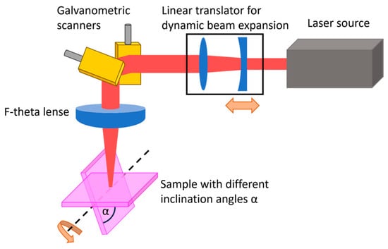
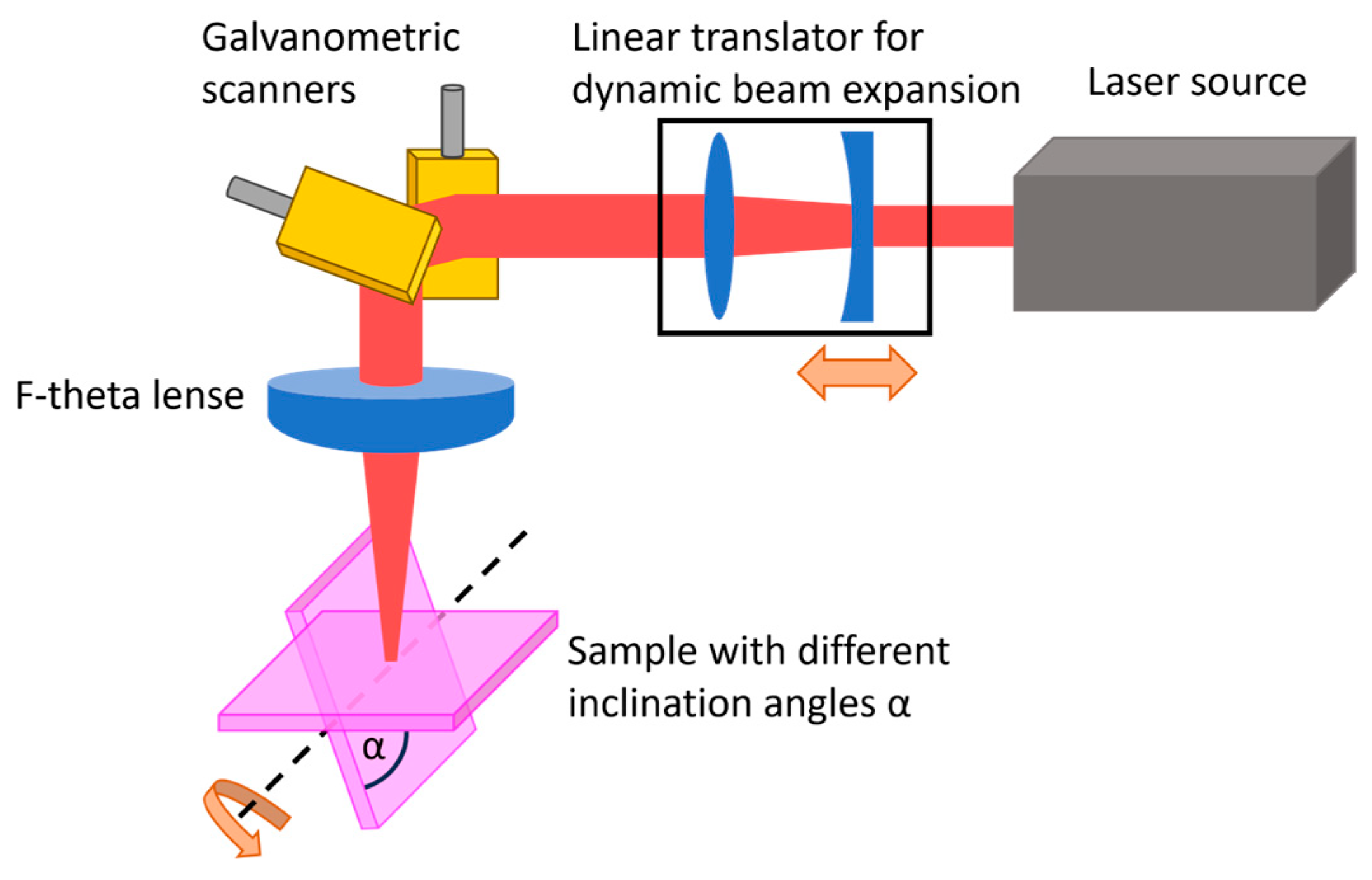
Figure 1.
Schematic of the laser system used with integrated linear translator for dynamic beam expansion which is done by moving one lens in respect to the other (indicated by double arrow). The sample can be rotated around the dashed line to structure at different inclination angles.
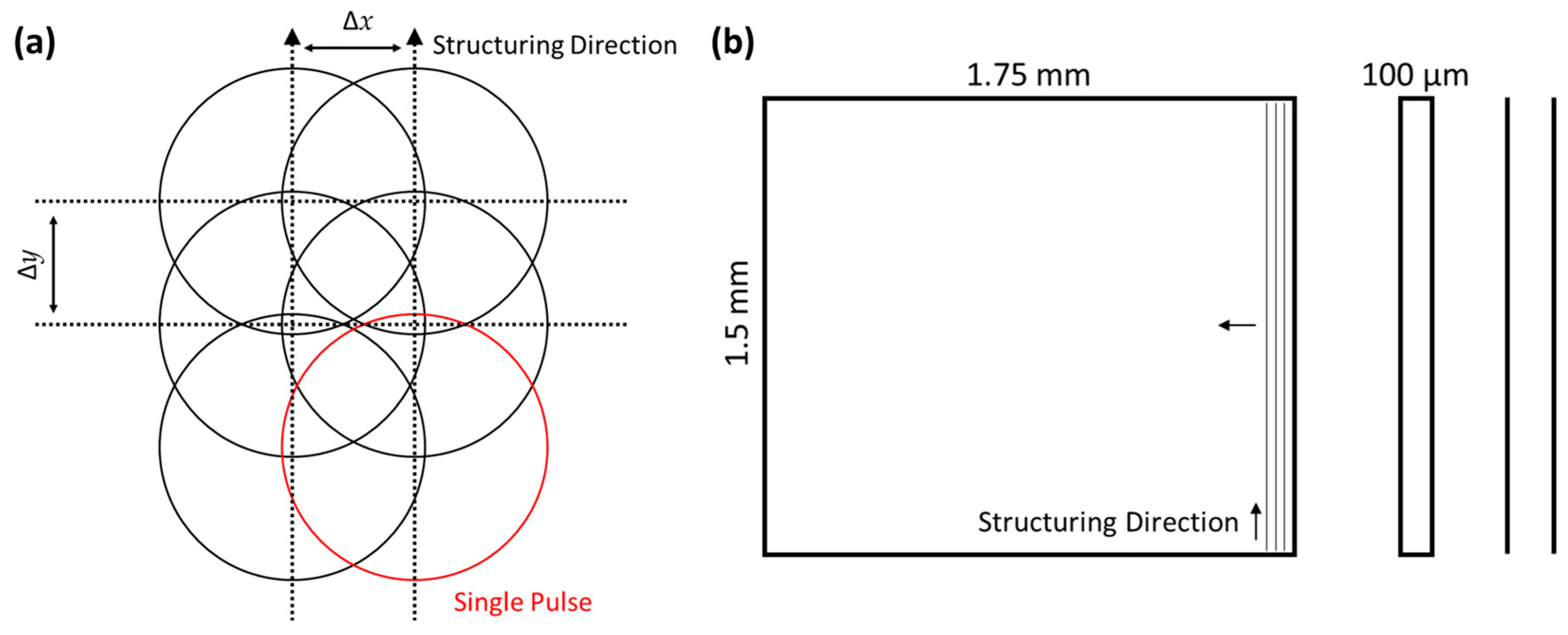
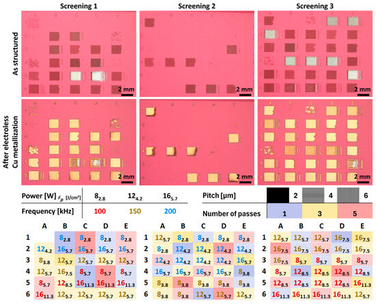
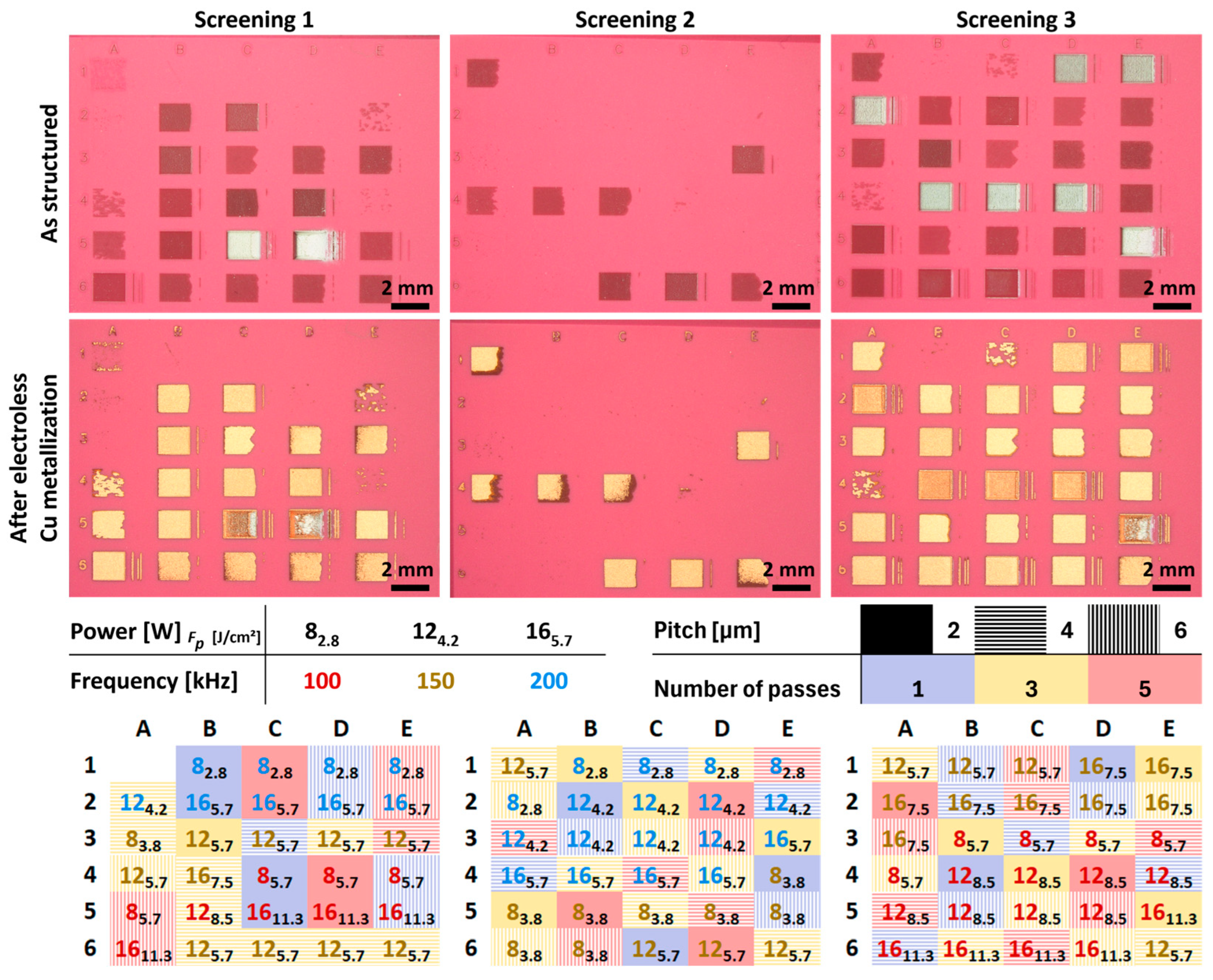
To investigate the effect of laser parameters, the power, pulse repetition frequency, pitch and number of passes were varied according to a full 34 factorial design of experiments (DOE) plan with 3 steps for each parameter. The pitch refers to the distance between the centers of two adjacent laser spots during structuring (Figure 2a) and is defined by the coefficient between marking velocity and the pulse repetition frequency. The pitch between the single marking lines ∆x was set to the same value as the pitch along the marking line to achieve a uniform structuring result. The power was varied between 8, 12 and 16 W, the frequency between 100, 150 and 200 kHz, the pitch between 2, 4, and 6 µm and the number of passes between 1, 3 and 5.
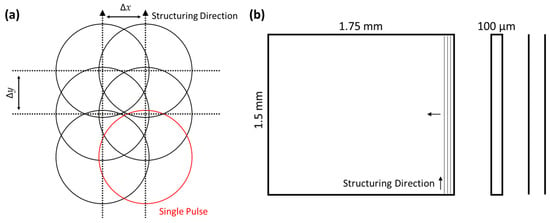
Figure 2.
(a) Visual depiction of pulse overlap and corresponding pitches. (b) Characterization layout for coarse parameter screening.
For a perfectly gaussian beam profile, the laser power P and the pulse repetition frequency f can be summarized into the maximum peak fluence FP that is calculated as follows:
with EPulse being the pulse energy, A the gaussian 1/e2 beam area and w the gaussian 1/e2 beam radius.
As the maximum peak fluence is only defined for a single pulse and does not reflect the pulse overlap, and respectively, the pitch, an accumulated fluence Facc can be used to describe the energy input during pulsed laser surface treatment [44,45,46], which considers the pitch and is calculated as follows:
with ∆x being the pitch between two hatching lines, ∆y the pitch between single laser pulses along the marking direction, v the laser marking velocity, P the measured average laser power and f the pulse repetition frequency. The number of passes Np was added to account for several laser passes. With this model, the average energy input over a 2D surface consisting of a grid of single laser pulses is estimated independently of the beam profile and beam diameter. The 2D surface is assumed rather large compared to the size of the single pulses and edge effects are neglected [44].
The DOE plan leads to a total amount of 81 parameter sets that were split up and partly randomized onto 3 samples. The central parameter setting of 12 W, 150 kHz, 4 µm and 3 laser passes was replicated 9 times over the different samples. The detailed parameter settings for each sample and the respective position can be found in the Supplementary Information (Tables S1–S3).
With each laser parameter set a rectangle of 1.75 × 1.5 mm2, a conductor line of 1.5 × 0.1 mm2 and two single laser lines with a distance of 150 µm were structured (Figure 2b).
Five laser parameter sets (Table 2) that showed promising plating results in the first screening were selected for structuring the characterization layout depicted in Figure 3 and used for a more detailed characterization. The design consisted of several circles with 900 µm diameter for adhesion strength measurements, a 1 × 13 mm2 track for tactile roughness measurement and smaller pads and tracks with different orientation to observe the uniformity of small feature structuring and metallization.
Table 2.
Laser parameter sets used for characterization of the metal layer properties.
Figure 3.
Layout used for characterization of metal layer properties with large pad for tactile roughness measurement and circles for adhesion measurements. The arrows indicate the hatching direction.
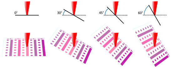
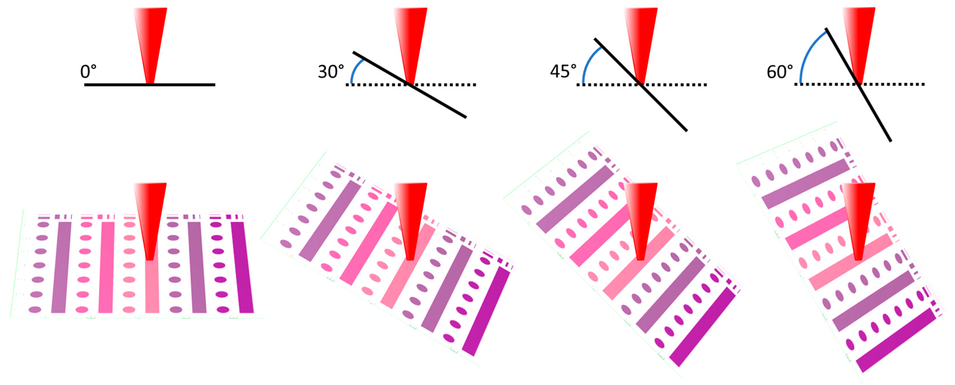
Layout 2 was then structured under different beam inclination angles. The angles were realized by tilting the sample stage by 30°, 45° and 60°. At 0° tilt the laser hits the sample normal to the surface as in standard planar processing (Figure 4). The hatching was done in a way so that a single hatching line could be structured without moving the focal point in z. The focal position was fixed on the sample surface using an integrated linear translator for dynamic beam expansion (varioSCAN, Scanlab, Puchheim, Germany) in front of the galvanometric scanners and the objective. All laser parameter settings were fixed as described in Table 2. The hatching distance between the hatching lines was angle compensated in order to preserve the pitch listed in Table 2. As the irradiated spot area enlarges due to the angled incidence, the peak fluence decreases with increasing structuring angle in accordance with Equation (1). The accumulated fluence remains constant with varied structuring angle as both ∆x and ∆y are kept constant (Equation (2)).
Figure 4.
Scheme of the characterization layout structured with varying laser incident angle which was achieved by tilting the sample in the depicted direction.
After laser structuring, the samples were ultrasonically cleaned with SurTec 026 (SurTec International GmbH, Bensheim, Germany) to remove all residual laser debris and contaminants from the surface, followed by a rinsing step in demineralized water. Samples were then immersed in the commercially available Circuposit 3350-01 (DuPont, Wilmington, NC, USA) electrolyte for the electroless copper deposition. The copper deposition was performed at 53 °C for 120 min after which the samples were dried at 80 °C for one hour. Samples used for detailed characterization and 3D samples were additionally plated with a standard electroless nickel and immersion gold finish (ENIG) (Ionogenic Palladium: Ronamerse Catalyst CF, DuPont, Wilmington, NC, USA, Nickel: Duraposit 88, DuPont, Wilmington, NC, USA, Gold: Aurolectroless SMT, DuPont, Wilmington, NC, USA).
The surface of each laser-structured substrate was studied with a white light interferometer (Contour GT-K, Bruker, Billerica, MA, USA) after laser structuring and after electroless copper deposition. The depth of the structured samples before and after plating was measured at the upper right edge of the structured 1.75 × 1.5 mm2 rectangle over an average of 500 µm in X and Y direction, and the difference between these two measurements was used to calculate the deposited copper thickness. The surface roughness Sa of the deposited copper was calculated on a 0.86 × 0.65 mm2 field according to ISO 25178 [47]. Prior to the roughness determination, a short wavelength pass Fourier filtering with a long wavelength cutoff of 0.25 mm was conducted to separate the waviness from the roughness.
Microscopy images of the copper-metallized 1.75 × 1.5 mm2 rectangles were analyzed by ImageJ 1.54g, using its “Analyze Particles” functionality to determine the metallized area fraction. The measured area of the metallized copper was divided by the size of the structured area (2.625 mm2) which resulted in the metallized area fraction. A metallized area fraction of 1 or 100% means a copper plating of the whole irradiated area, while a metallized area fraction of 0.5 or 50% means that only half of the irradiated area is plated.
The influence of the individual laser parameters on the ablation depth, the metallized copper thickness, the metallized area fraction and the resulting roughness as response variables was statistically analyzed using Minitab 18, considering the main effects and 2-factor interactions. A significance level of α = 0.05 was assessed for the analysis of variance (ANOVA) and insignificant terms were retained in the model. The model adequacy was evaluated based on R2, adjusted R2, predicted R2 and the lack of fit. The model assumptions were assessed by evaluating the residual plots.
SEM characterizations were carried out with a Helios NanoLab600 (FEI, Hillsboro, OR, USA). All samples were sputtered with a thin conductive carbon film prior to the investigations.
The adhesion strength was measured with a hot bump pull test using a Bondtester 4000Plus (Dage, Nordson, Westlake, OH, USA) described in detail elsewhere [31,48]. Briefly, a copper pin is soldered on a metallized pad with a defined geometry and then pulled vertically while measuring the pulling force. The maximum force before the solder breaks or before the metallization is pulled out of the substrate is measured and correlated with the respective metallized area to calculate a value for the adhesion strength. For statistics, 5 measurements were taken per sample.
The tactile roughness was measured with a Zeiss Surfcom 5000 (Carl Zeiss AG, Jena, Germany) surface profilometer according to the ISO 4287 [49], 4288 [50] and ISO 3724 [51] with a measurement length of 12.5 mm and a cutoff wavelength of 2.5 mm. For statistics, 3 measurements were taken per sample.
The mounting of SMD components was carried out with standard SAC solder (F169, Heraeus, Hanau, Germany) and a standard reflow solder process with a peak temperature of 255 °C.
3. Results
3.1. Influence of the Laser Processing Parameters on Ablation and Metallization
3.1.1. Optical and Topographic Analysis
The initial optical analysis of the laser parameter screening samples (Figure 5) shows that the investigated parameter range results in structured fields with differing discoloration that leads to a variation in the metallization results. Similar results have been reported on Al2O3 ceramics, linked to the varied amount of deposited laser energy across parameter combinations with higher energy densities resulting in a darker discoloration [52]. Here, parameter sets with darker discoloration show a higher probability for a metallization with a metallized area fraction close to 100%, whereas parameter sets with a light discoloration tend to show only partial metallization with metallized area fractions < 90%. Regions with white discoloration also show copper deposition, but with an inhomogeneous appearance. Irradiated areas without discoloration showed no successful plating.
Figure 5.
Microscopic images of the samples from the laser parameter screening. Images have been taken after the laser structuring and after the electroless copper metallization. Below each image a spatially resolved parameter map is given with the respective parameter coding.
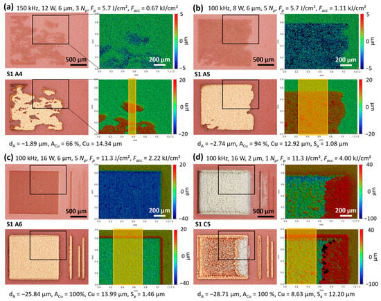
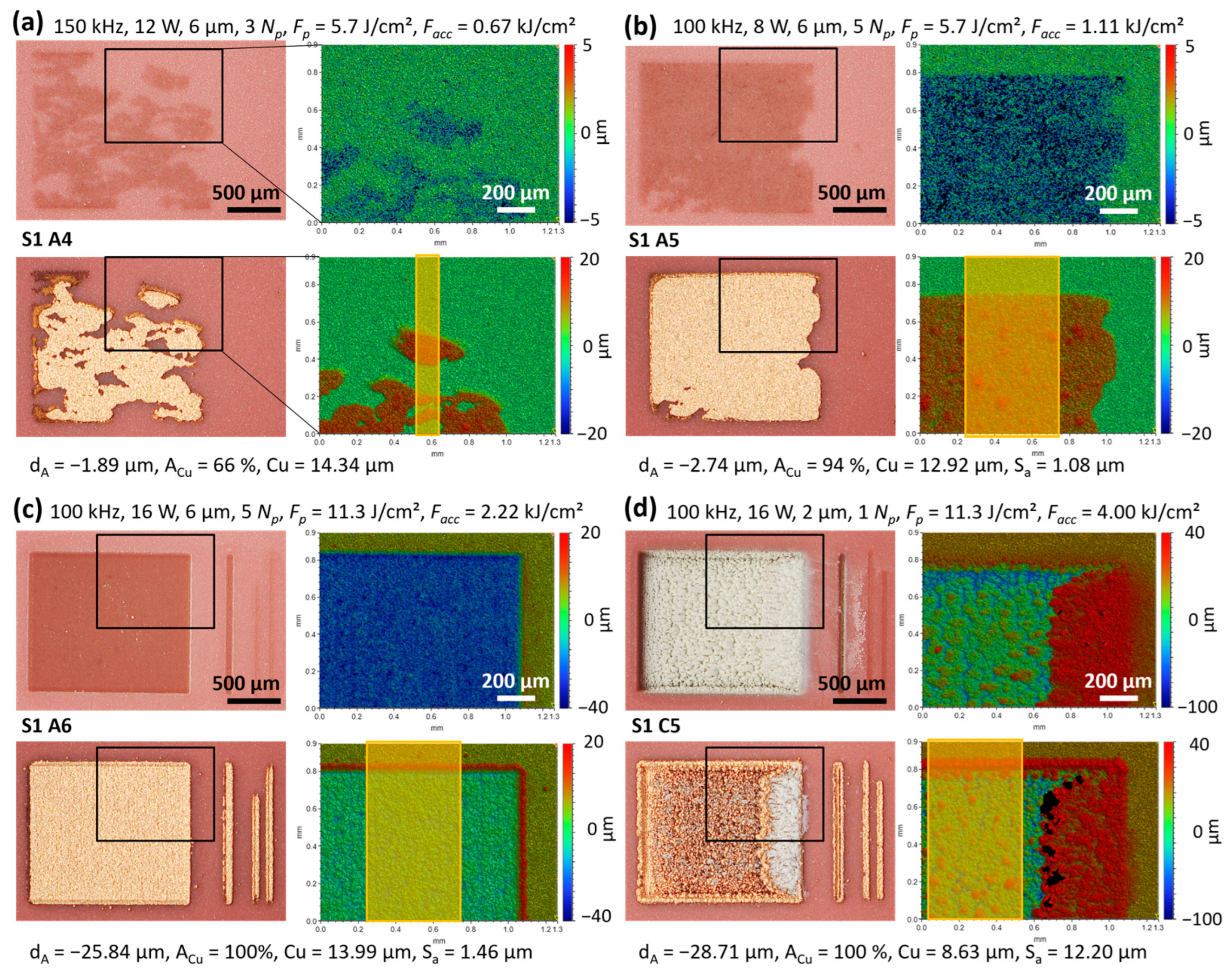
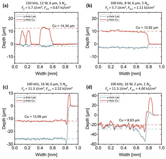
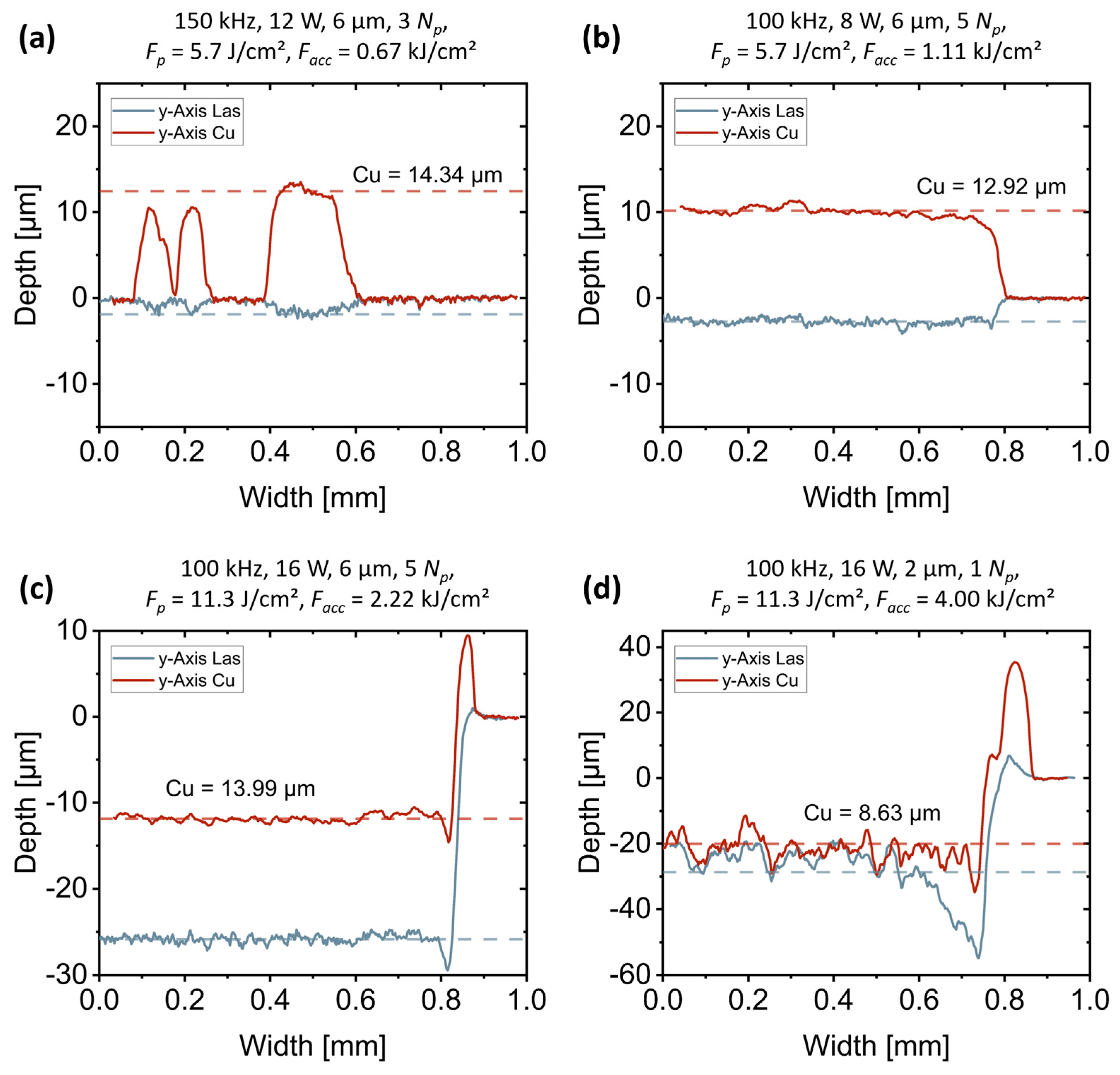
A detailed inspection of four selected laser parameter sets is depicted in Figure 6. Here, the microscopic image of the structured and metallized area is paired with the respective topography image of the white light interferometer measurement. The corresponding height profiles are depicted in Figure 7. In Figure 6a,b it can be clearly seen that only areas showing a visible discoloration experienced ablation, and only ablated areas tend to subsequently metallize. Figure 6c displays a combination of laser parameters yielding a complete metallization, with a metallized area fraction of 100% of the larger structured areas and almost fully metallized single lines, implying an almost ideal laser activation. Under these conditions, the plated copper has a measured thickness of 13.99 µm and a surface roughness of Sa = 1.46 µm. In contrast, Figure 6d shows that the white discoloration is due to a very high roughness in the structured area. In addition, a significant amount of ablated material appears to be redeposited at the right edge of the structured area. The high roughness in Figure 6d can also be observed in the height profile (Figure 7d) limiting the measurement of the copper thickness.
Figure 6.
Microscopical and topography images of four different laser parameter sets (a–d) after laser structuring and after electroless copper deposition. The area of the topography measurement is drawn into the microscopic image. Listed above each parameter set is the respective position (cf. Figure 5), the laser parameters and the corresponding peak fluence Fp. Below each parameter set, the depth after ablation (dA), the metallized area fraction in reference to the structured area (ACu), the calculated copper thickness (Cu) and the surface roughness (Sa) is written. The yellow area in the lower right image of each parameter set is the width that was used for the extraction of the average height profiles, which are depicted in Figure 7. The same position was used for both structured and metallized samples.
Figure 7.
Average height profiles of four different laser parameter sets (a–d) corresponding to the depicted laser parameter sets in Figure 6. The dashed lines represent the measured height after structuring and after copper deposition. The calculated copper thickness is inserted.
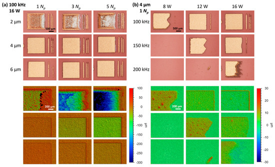
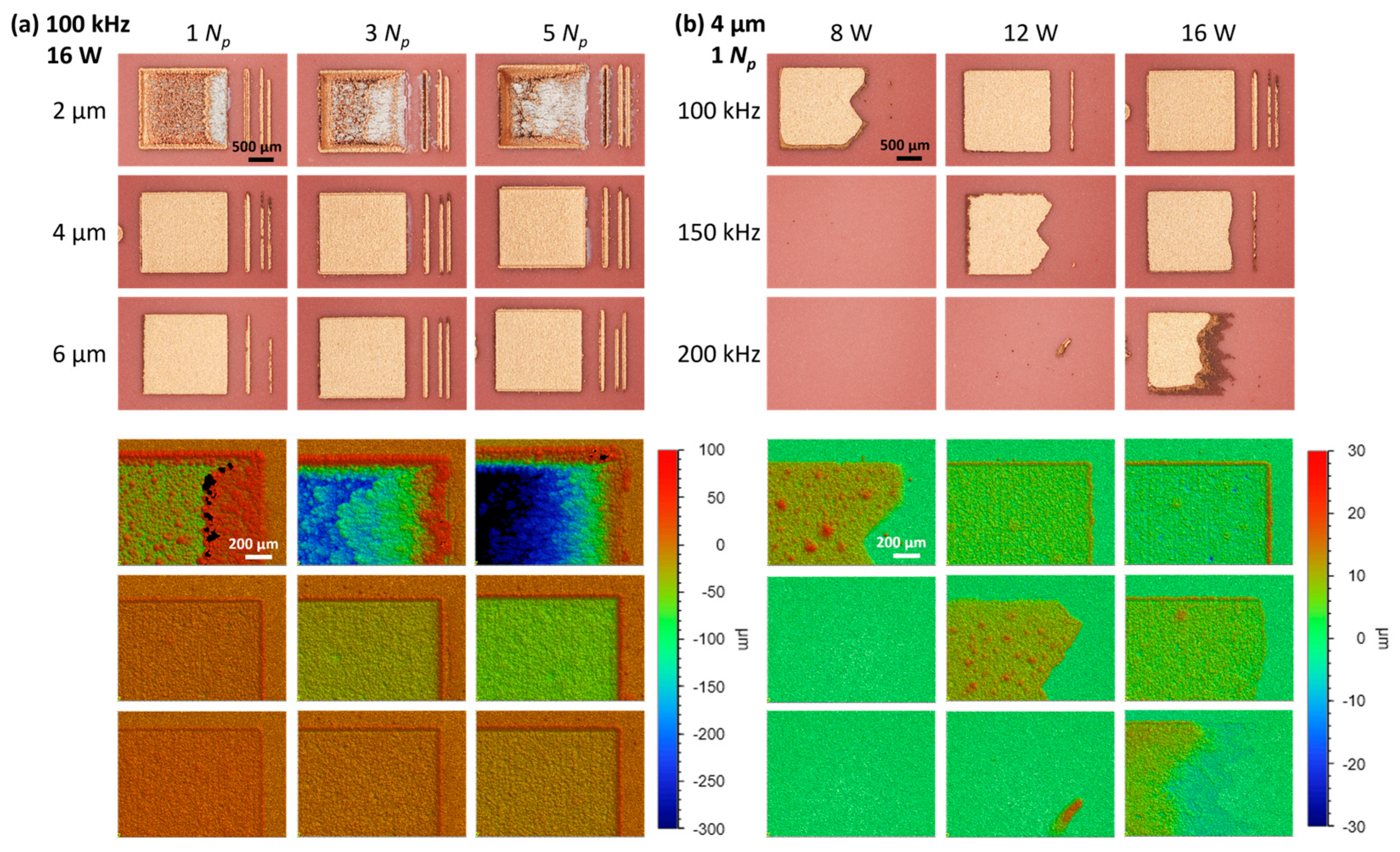
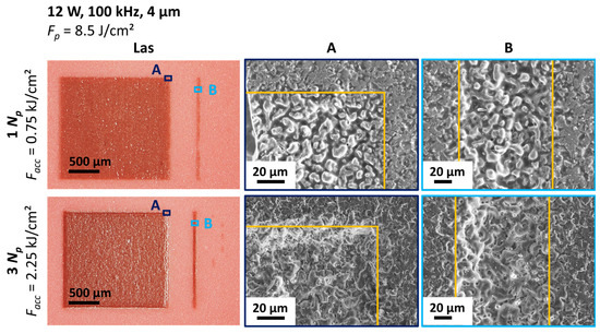
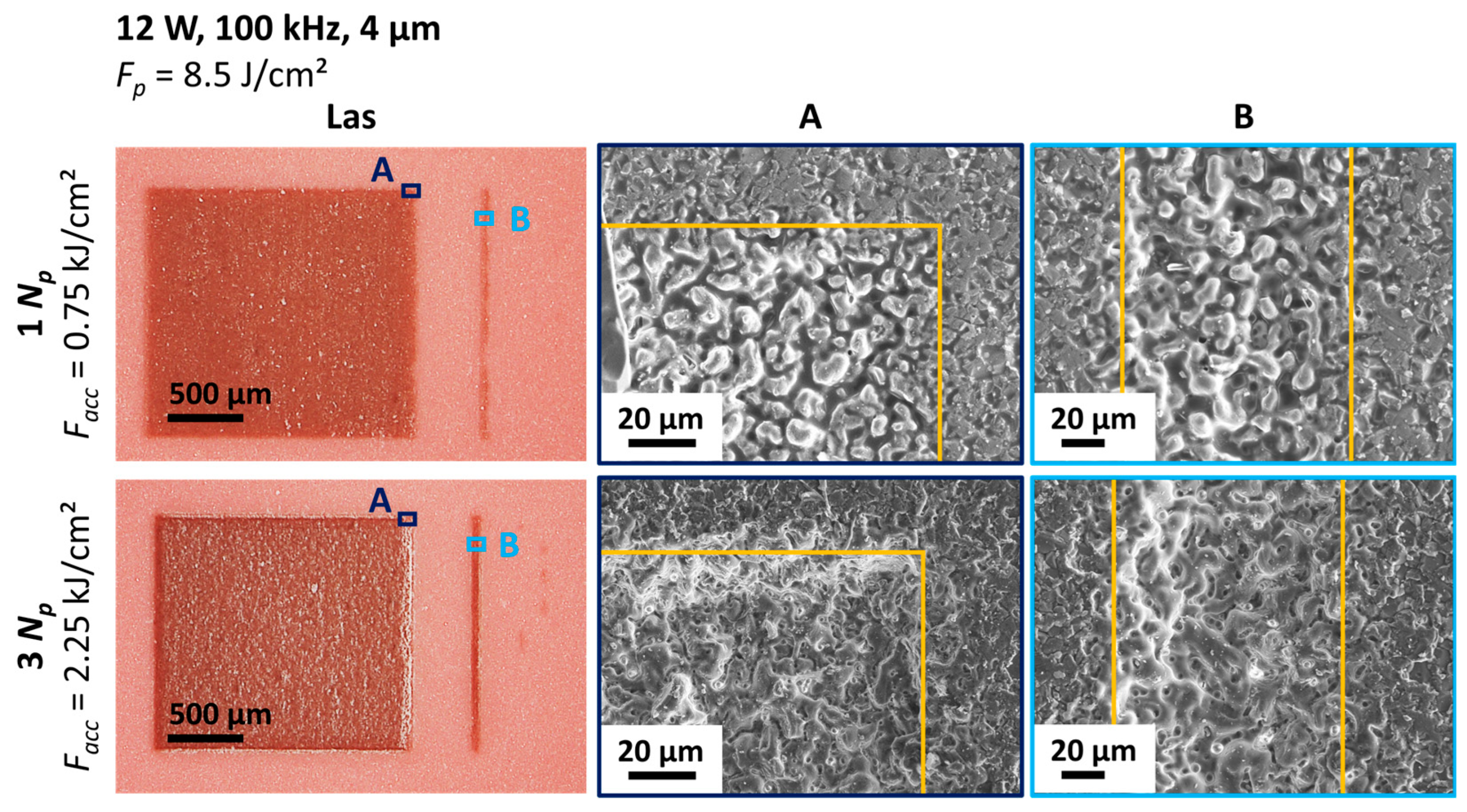
In the next step, the influence of individual laser parameters (pulse repetition frequency, average laser power, pitch and the number of passes) was studied. In Figure 8a, the pitch (2, 4, 6 µm) and the number of passes (1, 3, 5) were varied, while the laser power and pulse repetition rate were kept constant at 16 W and 100 kHz, respectively. It can be seen that the pitch and the number of passes do not have a significant effect on the metallized area fraction, but rather on the ablation depth. Supplementary SEM investigations show that the ablation is accompanied by a change in the sample’s surface. It appears partially melted and re-solidified. This effect increases with a larger number of passes (Figure 9). When keeping the pitch (4 µm) and number of passes (1) constant and varying the laser power (8, 12 and 16 W) as well as the pulse repetition rate (100, 150 and 200 kHz), the laser activation strongly varies. Figure 8b shows that these parameters have a large influence on the resulting metallized area fraction.
Figure 8.
(a) Influence of pitch and the number of passes and (b) of the average laser power and the pulse repetition frequency on the observed metallization with the corresponding topography images of the metallized areas.
Figure 9.
SEM images of laser-structured areas. Upper images are from a parameter with 1 laser pass, lower images from the same parameter with 3 laser passes. The laser-marked area is indicated by the yellow lines.
In Figure 8b another interesting detail can be observed concerning the already mentioned and briefly discussed parameter fields with partial ablation (e.g., 8 W, 100 kHz, 4 µm, 1 Np). On the right side of the structured area where the structuring starts (c.f. Figure 2b), no ablation and therefore no copper deposition can be observed. The further the laser moves to the left side of the structured area (in the direction of scanning), at some point ablation and metallization starts and is then present over the whole width of the field. A closer look at Figure 6a also shows this behavior in a way that the ablated and metallized islands get bigger towards the left side of the structured area.
3.1.2. Statistical Analysis of the Influence of Laser Parameters
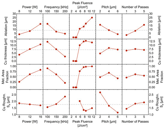
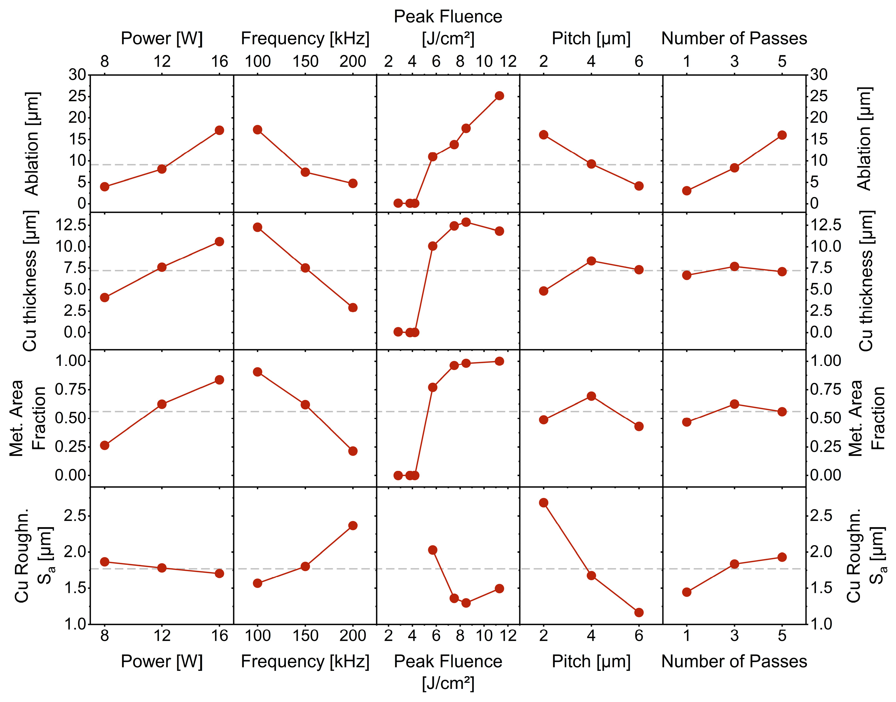
The experimentally measured mean responses of the ablation, the resulting copper thickness, the metallized area fraction and the resulting roughness in relation to the laser processing parameters (laser power, pulse repetition frequency, peak fluence, pitch and the number of passes) are depicted in Figure 10. The parameter sets which exhibited a large redeposition and therefore showed a white discoloration (cf. Figure 5) were excluded from the analysis. As most of the fitted factorial models showed a significant lack of fit, they were not used for quantitative prediction or process optimization. The fitted models with their respective ANOVA tables, the model’s summary statistics, the pareto diagrams and the residual plots can be found in the Supplementary Information (Tables S4–S13, Figures S1–S16).
Figure 10.
Main effects plots of the experimentally measured mean responses of the ablation, the resulting copper thickness, the metallized area fraction compared to the structured area and the resulting roughness in relation to the laser processing parameters (laser power, pulse repetition frequency, peak fluence, pitch and the number of passes). The grey dashed line represents the overall mean value of the respective response variable. The fields with large redeposition with the white coloration depicted in Figure 5 were excluded from the analysis, which resulted in a total of 80 parameter sets analyzed. The copper roughness was only considered from fields which exhibited metallized area fractions above 85%, which resulted in a total of 54 parameter sets analyzed.
All input variables have a significant effect on the ablation, with the peak fluence, which combines power and frequency (Equation (1)), being the most significant parameter. The peak fluence is also the dominant factor in the resulting copper thickness and metallized area fraction, while the pitch and the number of passes have a medium and a small influence respectively. The copper roughness was only analyzed on laser parameter sets, from which the metallized area fraction was above 85%. The pitch was found to be the dominant factor for copper roughness, followed by the frequency. The number of passes and the laser power only have a medium influence on the roughness.
It was further identified that below a peak fluence of 5.7 J/cm2 no ablation and therefore no copper deposition occurs. For higher values, the ablation increases and the Cu thickness reaches a plateau. This can also be observed by comparing the height profiles of the structured areas in Figure 7a–c.
Complete plating with an area fraction close to 1 can be observed from peak fluences above 7.5 J/cm2. Surface roughness is minimized at peak fluences around 8.5 J/cm2 and increases again for larger peak fluencies.
3.1.3. Relationship Between Ablation and Accumulated Fluence
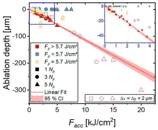
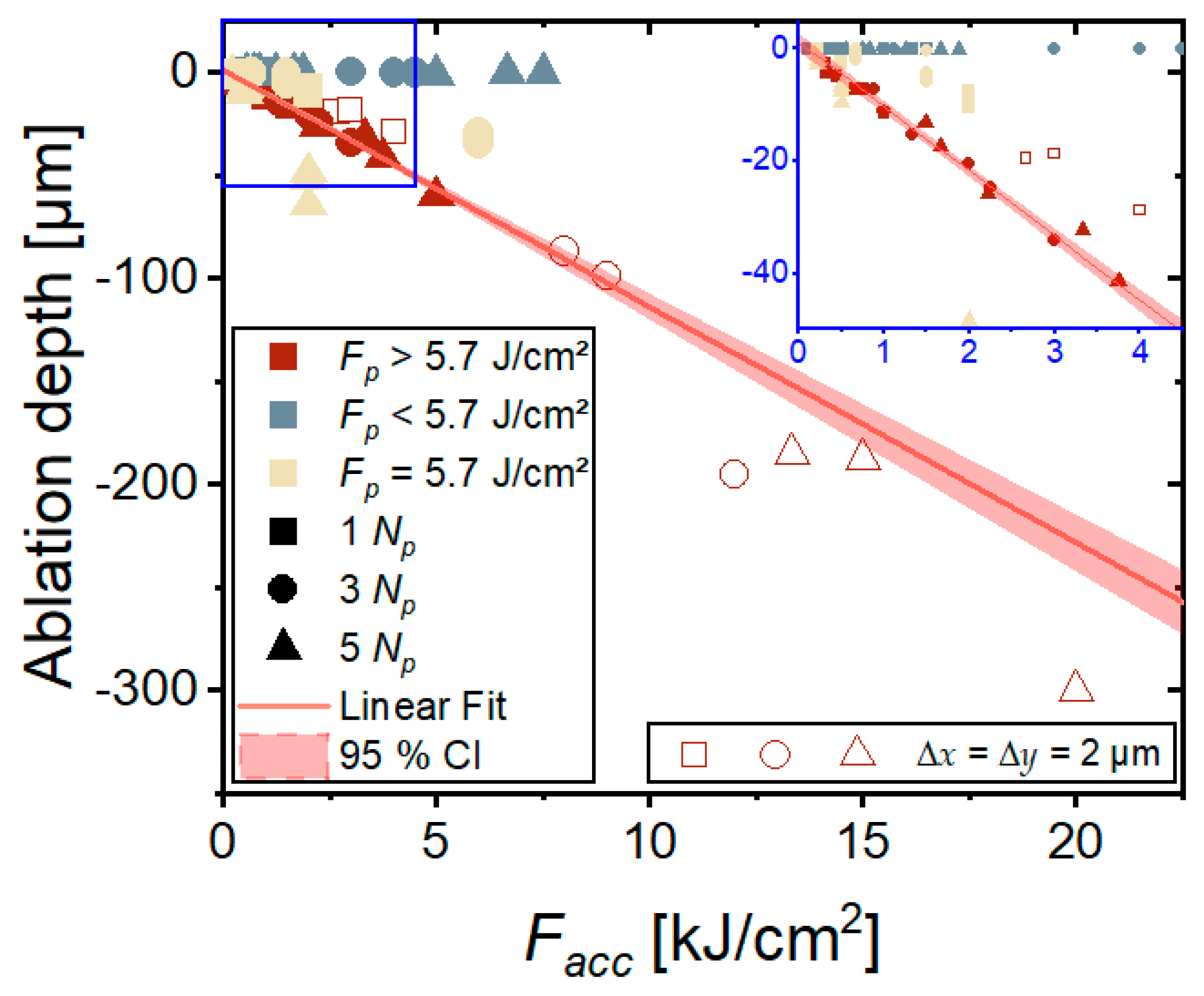
The relationship between the accumulated fluence and the resulting ablation depth is depicted in Figure 11. Parameter sets that resulted in areas with white discoloration after laser structuring and redeposition of ablated material (Fp > 5.7 J/cm2, ∆x = 2 µm) were not included in the analysis.
Figure 11.
Diagram of the ablation depth vs. the accumulated fluence; measurements of the ablation depth are labelled with respect to the number of passes and peak fluence. Open symbols describe the samples with white discoloration and redeposition as result of peak fluences above 5.7 J/cm2 and a pitch of 2 µm (c.f. Figure 5), of which an accurate measurement of the ablation depth was not possible. The inset shows an enlarged view of the parameter sets with a low accumulated fluence. The linear regression of parameters with Fp > 5.7 J/cm2 and ∆x > 2 µm is plotted alongside with the confidence band. Linear fit parameters are listed in Table 3.
From the plot, it can be clearly seen that independently of the accumulated fluence, and therefore of the pitch, no ablation can be observed at a peak fluence below 5.7 J/cm2, while for peak fluences above 5.7 J/cm2 the ablation increases linearly with increasing accumulated fluence. A respective linear fit is included in Figure 11 and the respective fit parameters are listed in Table 3. Parameters with a peak fluence of 5.7 J/cm2 show no clear trend concerning the accumulated fluence.
Table 3.
Results of the linear regression of the ablation depth in relation to the accumulated fluence (cf. Figure 11).
3.1.4. Adhesion Strength of the Deposited Copper Layers
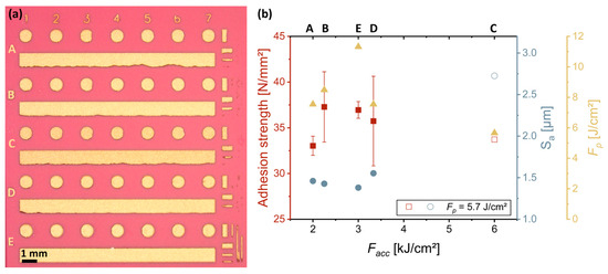
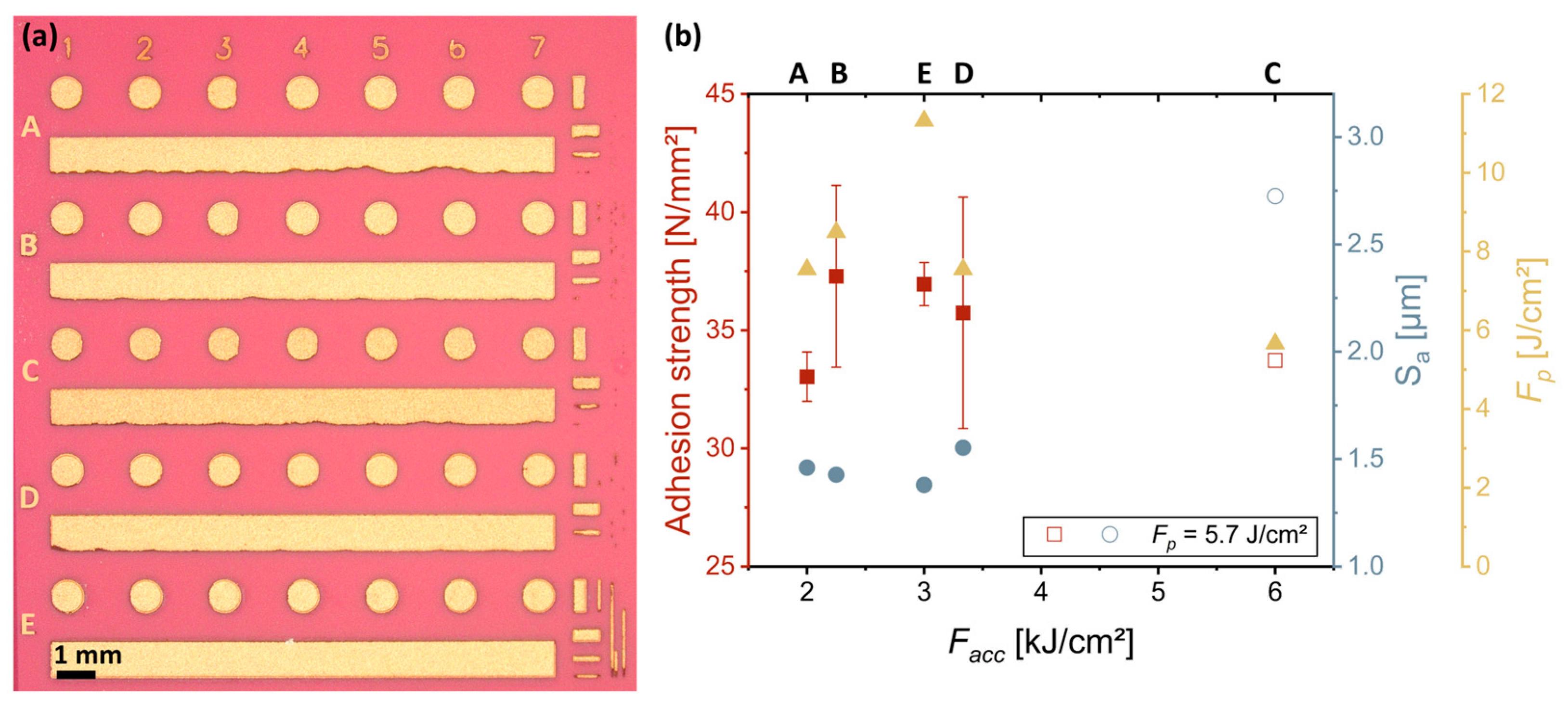
Adhesion strength analysis of a representative sample structured with selected laser parameter sets is depicted in Figure 12. For each laser parameter set the mean value ± the sample standard deviation is plotted against the accumulated fluence alongside the respective peak fluence. It can be observed that the adhesion strength for all structured parameter sets lies in between 33 and 37 N/mm2, reaching the highest value at intermediate accumulated fluences of around 3 kJ/cm2. Peak fluence is found to directly correspond to adhesion strength, with high peak fluence values resulting in the highest adhesion strength and smaller peak fluences showing a reduction in adhesion strength. The parameter set E with Facc = 3 kJ/cm2 and Fp = 11.3 J/cm2 shows the lowest surface roughness of Sa = 1.38 µm with an adhesion strength of 36.95 ± 0.91 N/mm2 and is therefore considered as the optimal laser parameter set (100 kHz, 16 W, 4 µm, 3 Np) for further tests. The roughness was found to be inversely related to the measured adhesion strength, with parameter combinations producing the lowest roughness exhibiting the highest adhesion strength. The increasing of surface roughness did not necessarily increase the adhesion strength.
Figure 12.
(a) Microscopic image after electroless plating of the characterization layout. The distinctive laser parameter set description can be read out of Table 2. (b) Measured adhesion strength, measured surface roughness and respective peak fluence of the laser parameter set in relation to the accumulated fluence of the respective laser parameter sets from (a).
3.2. Influence of Laser Incident Angle on Activation and Metallization
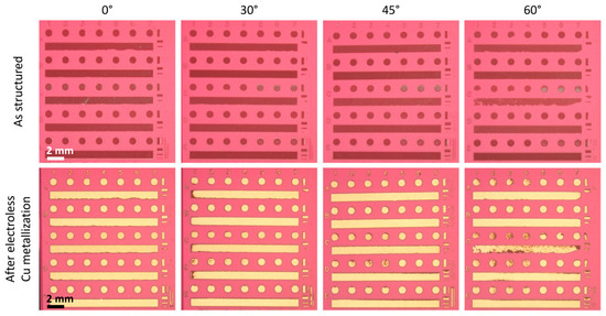
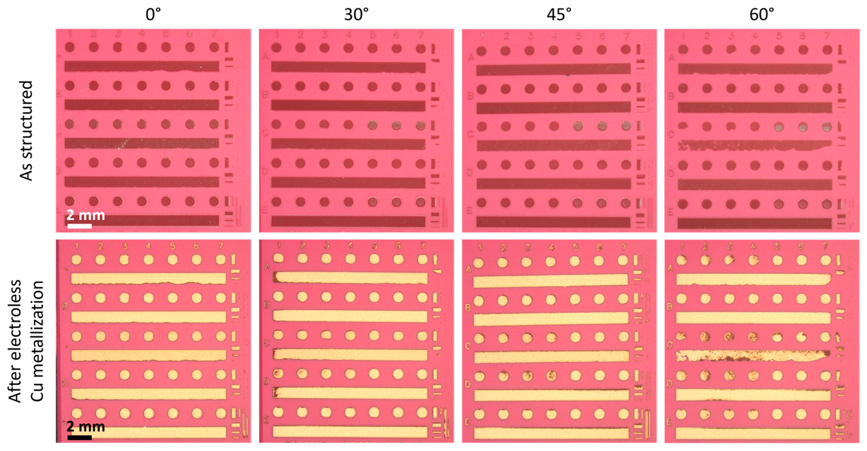
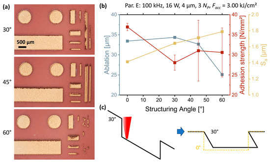
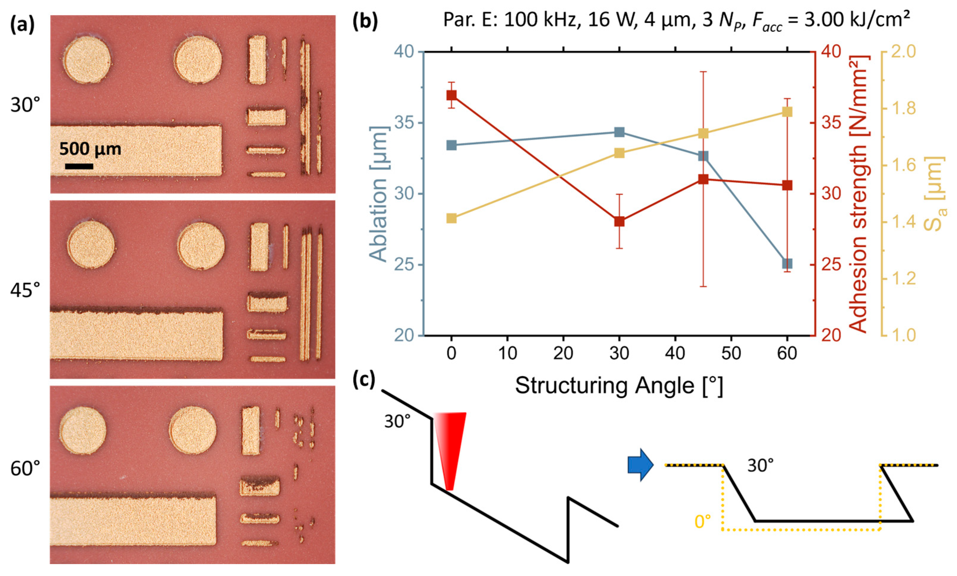
The impact of the laser incident angle used for structuring can be observed in the structuring and metallization results of the characterization layouts depicted in Figure 13. General activation and metallization can be observed to work well over all parameter sets and angles. Even at maximum incident tilt angle (60°) most parameter sets show a full metallization of the structured areas. The only parameter set showing a visible decrease in activation is parameter set C with Facc = 6.00 kJ/cm2, corresponding to the parameter set with the lowest peak fluence of Fp = 5.7 J/cm2 at 0° structuring angle.
Figure 13.
Structuring and metallization results of the samples structured with the characterization layout with varying laser incident angles.
In-depth analysis of parameter set E with Facc = 3.00 kJ/cm2, which was the best parameter set on the planar test above, is depicted in Figure 14a. Larger pads can be observed to metallize over the whole structured area, even at large tilt angles. Smaller pads and lines show a declining activation with increasing tilt angle. The evaluation of the ablation on the large pad in Figure 14b shows that the ablation decreases with increasing structuring angle. The reduction in ablation depth with increasing tilt angle can be well explained by considering the ablation geometry depicted in Figure 14c. Structuring of a tilted surface results in cavities normal to the laser incident direction, while the ablation depth is measured relative to the surface normal, and is therefore smaller than the measured ablation depth considering the same ablation without sample tilt. The measured adhesion strength slightly declines with increasing structuring angle but stays high with an average value of over 30 N/mm2 at 60°. Both the mean variation of the measured values as well as the measured surface roughness increase with increasing structuring angle.
Figure 14.
(a) Microscopic images of the metallized structures of laser parameter set E (100 kHz, 16 W, 4 µm, 3 Np, Facc = 3.00 kJ/cm2) with different structuring angles. (b) Measured values of the ablation, the adhesion strength and the surface roughness of laser parameter set E in relation to the structuring angle. (c) Scheme of the ablation of tilted surfaces to show that smaller ablated depths can be expected at inclined angles. The taper angle at the side walls is not shown here for simplification.
3.3. Electrical Characterization and Metallization of 3D Ceramic Substrates
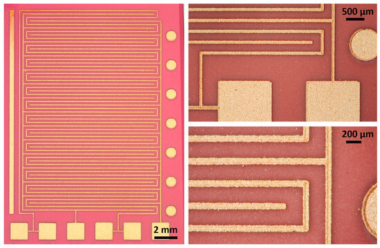
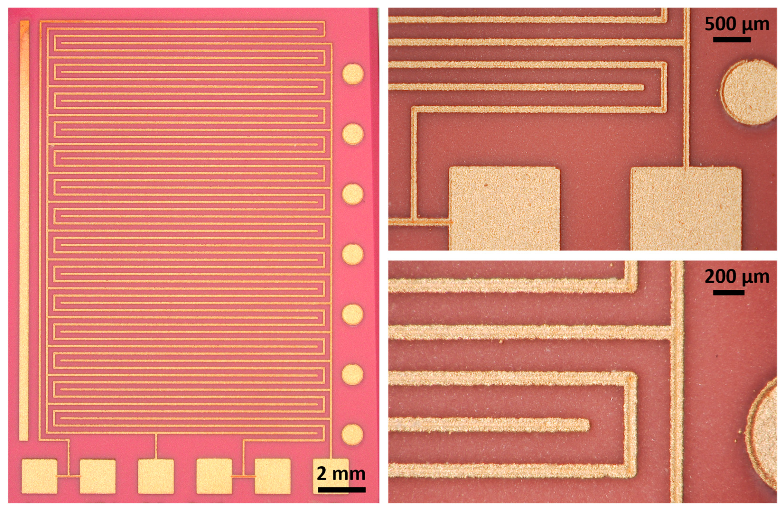
With the previously established optimal parameter combination (100 kHz, 16 W, 4 µm, 3 Np), meander structures of 369 mm length combined with interdigital structures have been fabricated. The laser-based fabrication was able to produce tracks of 100 µm width separated by 200 µm. A representative metallized sample is depicted in Figure 15. No short-circuits could be measured between the interdigital structures and the meander across all three sample replicates. The measured four-point resistance of the meanders was 9.27 ± 0.40 Ω. Tactile roughness measurements performed on the long track on the left side of the sample displayed roughness values of Ra = 0.87 ± 0.01 µm and Rz = 7.47 ± 0.47 µm.
Figure 15.
Microscopic images of the fabricated meander and interdigital structures structured with 16 W, 100 kHz, 4 µm pitch and 3 laser passes.
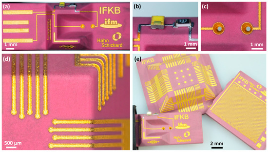
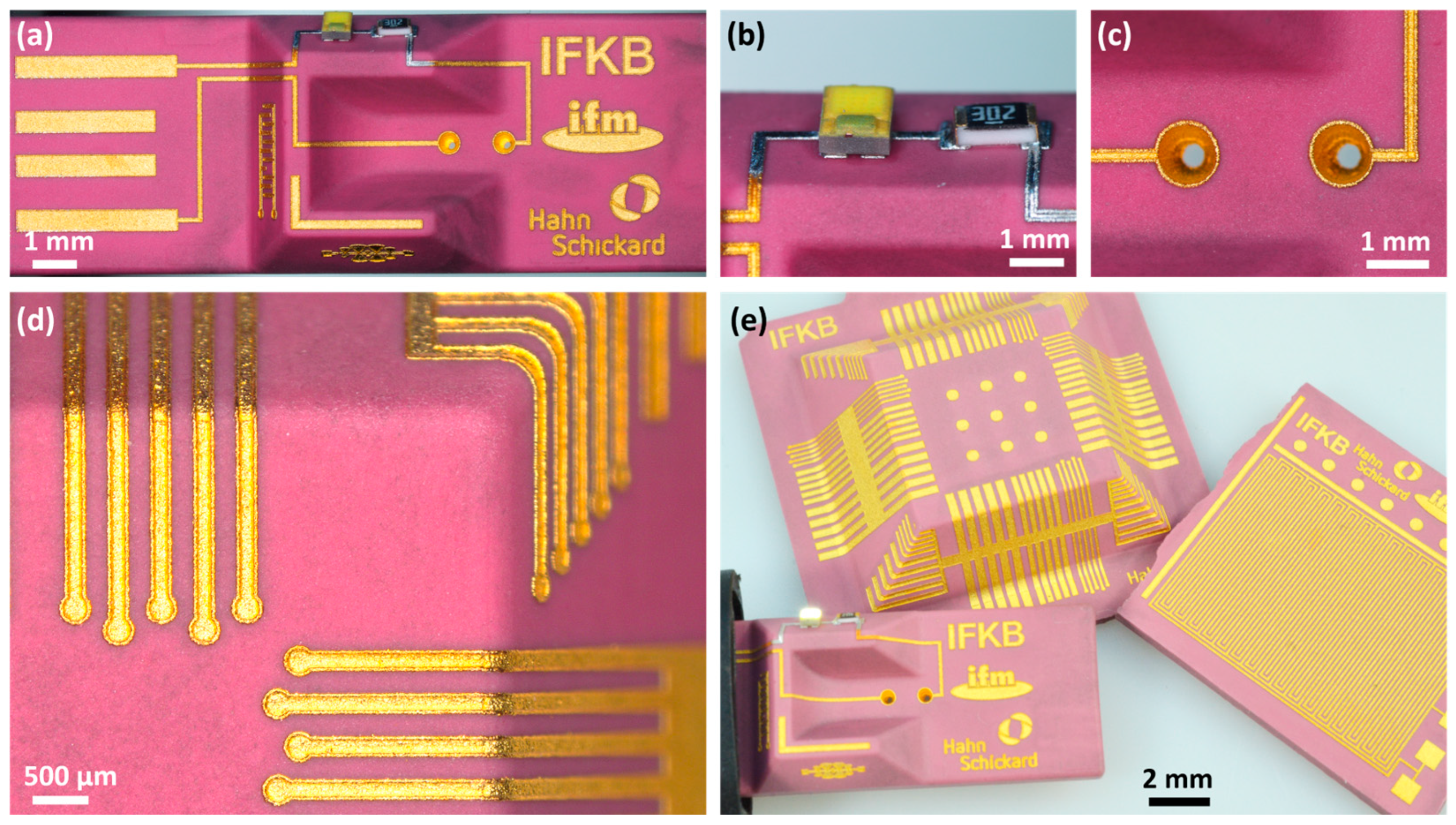
Additionally, two 3D geometries, a “USB-Demo” (Figure 16a) and a “Pyramid-Demo” (Figure 16d) were structured with the selected optimal laser parameter set and metallized with electroless copper and an ENIG finish. The “USB-Demo” was fabricated with laser-drilled vias (Figure 16c), which are connected on the backside. On one side of the “USB-Demo” a high-power LED and a resistor were mounted (Figure 16b). The LED can be powered by inserting the demonstrator in a USB port (Figure 16e).
Figure 16.
Fabricated 3D technology demonstrators. “USB-Demo” (a) with soldered components (b) and laser drilled and metallized vias (c) and enlarged view of “Pyramid-Demo” (d). (e) Different metallized 3D parts with working LED on “USB-Demo” and “Pyramid-Demo” above.
4. Discussion and Comparison with Literature
It could be successfully demonstrated that Cr2O3-doped ZTA ceramics can be selectively metallized after irradiation with an infrared nanosecond pulsed laser. The deposited copper thickness is not dependent on the ablation depth, implying that there is a minimum activation threshold which must be overcome to initialize successful metallization. The peak fluence was observed to be the most dominant factor for ablation and therefore also for the activation and subsequent copper deposition. For homogeneous ablation of the whole irradiated surface, a high peak fluence and small pitches ≤ 4 µm are necessary. If functionalization techniques such as wire bonding follow, for which a low roughness is needed, the peak fluence has to be restricted and care has to be taken to use larger pitches, as the roughness exhibits a minimal value at intermediate peak fluences around 8.5 J/cm2 and increases with smaller pitches. For parameter sets with a peak fluence of 5.7 J/cm2, the ablation only happens partially and creates ablated islands, which grow in the direction of scanning. These observations indicate that the multi-pulse ablation threshold for the investigated Cr2O3-doped ZTA ceramic lies in the range of 5.7 J/cm2 and that some kind of incubation effect is present. This complies well with literature values, where the multi-pulse ablation threshold for undoped Al2O3 during nanosecond infrared laser processing was determined to be 8.2 J/cm2 [53], and it was also previously shown that adding ZrO2 to Al2O3 leads to a decrease in the ablation threshold [54]. Concerning the incubation effects observed, it has already been reported in the literature that at peak fluences around the ablation threshold, defects such as grain boundaries or ZrO2-rich areas can foster the ablation. Such ablated regions then act as new defect regions, at which laser absorption is further enhanced. Han et al., for example, reported a preferential absorption of zirconia-rich areas during ultrashort laser processing of ZTA ceramics, which then leads to an eruption of the Al2O3 phases [55]. The changed roughness of the first ablated areas [56,57] and the resulting heat, which is transferred into the sample [58], then lowers the ablation threshold for further incoming pulses. Another effect that could play a role for this observation is the thermochromic behavior of Cr2O3-doped Al2O3, which becomes darker, or more greyish, when heated [59,60]. A darker material may also lead to a decrease in the ablation threshold, as more laser light is absorbed in surface near areas.
It could be observed that for parameter sets that yield a peak fluence greater than 5.7 J/cm2 and where large redeposition does not occur (∆x > 2 µm), the ablation can be well predicted with the accumulated fluence. As in the accumulated fluence, all relevant laser parameters, especially also the pulse overlap and the number of passes, are considered, this is an interesting result. In most other publications the pulse overlap, or the number of pulses during laser structuring and the respective single pulse laser parameters (pulse energy, peak fluence), are considered as individual variables. Umer et al. [52] and Mohammed et al. [61], for example, examined the microsecond infrared laser milling of Al2O3 ceramics and reported that pulse intensity and the pulse overlap have a significant effect on the ablation depth, but the combination of both parameters was not analyzed. Sajti et al. investigated the ablation efficiency of Al2O3 during nanosecond laser machining but also only evaluated the pulse energy, pulse distance and repetition frequency individually [62]. Han et al. examined the femtosecond infrared laser milling behavior of ATZ/ZTA composites and reported that the material removal rate is mainly dependent on the laser pulse energy and varying scan speeds has a minor effect. However, also here, the effect of the accumulated fluence was not investigated [54].
The electroless-deposited copper layers show reliable adhesion of up to 37 N/mm2, which is well above previously reported values on laser-induced metallization on Al2O3-based ceramics, as compared in Table 4. Moreover, the resulting roughness of the metallization was comparably low with values of Ra < 0.9 µm and Rz < 8 µm. As wire bonding of 25 µm Al wires has already been successfully demonstrated on LDM metallized ceramics with Rz = 8 µm [32], it is assumed here that the low roughness of the fabricated samples in this study should be likewise sufficient for a successful wire bonding.
Table 4.
Comparison of different studies on laser-induced direct metallization of Al2O3-based ceramics, where the roughness and/or the adhesion strength of the metallization were measured.
It was further shown that a successful activation and metallization can be done on tilted surfaces without a drastic decrease in adhesion strength or increase in roughness.
The findings and results of this study have to be interpreted alongside its limitations. As only a few laser parameter sets have been analyzed concerning their adhesion strength, the general effects of the laser processing parameters on the resulting adhesion strength cannot be interpreted in detail. Additionally, more quantitative statistical analysis would strengthen the observed trends, since only a few samples were analyzed.
5. Conclusions and Outlook
In summary, with the presented combination of well-tuned laser parameters, the activation and metallization of complex 3D-shaped chromium-doped ZTA ceramics was successfully demonstrated using digital and maskless processes. The presented results show that the use and design of ceramic circuit carriers can be extended to the third dimension, which opens up new possibilities for ceramic packaging and system integration.
The key findings of this study are:
- Ablation is necessary for a successful activation and once ablation happens, metallization occurs independently of the ablation depth.
- Below a peak fluence of 5.7 J/cm2, no ablation occurs.
- For large peak fluences (11.3 J/cm2) and small pitches (2 µm), redeposition can occur which leads to very rough surfaces and an inhomogeneous copper deposition.
- For peak fluences above 5.7 J/cm2 and when no redeposition occurs, the ablation can be well predicted with the accumulated fluence which includes the pitch and therefore all relevant laser parameters.
- The peak fluence is the governing factor for the ablation and therefore for the activation and copper deposition. But with increasing peak fluence, the roughness of the metallization also increases.
- Deposited copper layers show an adhesion of up to 37 N/mm2 and a roughness of Ra < 0.9.
- Fabricated 369 mm long meander structures show resistances of 9.27 ± 0.40 Ω with track widths of 100 µm and isolation widths of 200 µm showing no short-cuts or interruptions.
- Structuring under inclined angles of up to 60° leads to an increase in the roughness of the deposited copper layers from Sa = 1.4 µm to Sa = 1.8 µm, while the adhesion strength remains above 30 N/mm2.
Further experimental proof is needed on the observed linear relationship between the accumulated fluence and the measured ablation for different materials and ceramic compositions and different laser systems with different wavelengths and pulse durations. Additional research is still needed to gain a better understanding of the interplay between the used laser wavelength and pulse duration and the respective ceramic composition, enabling insight into the underlying activation mechanism. Thus far, Xu et al. [43] have completed some investigations into the activation mechanism after nanosecond infrared laser irradiation, and they infer that the main catalytic activity comes from a hydroxylation of the surface after laser structuring. They did not find any evidence of a promotion of oxygen vacancies and an enhancement of electron–hole pairs, which are alternate hypotheses [21,22]. However, Xu et al. investigated these hypotheses on bulk samples, and as the laser only influences the top few nanometers of the structured area, the analyses of bulk material might not resolve these phenomena. The hypothesis of laser-induced mechanical stresses, which alter the band gap and therefore lead to a catalytic activity of the surface [21], also deserves consideration. Therefore, concerning the respective activation mechanism that enables the electroless copper deposition after laser irradiation, further research is still needed.
Supplementary Materials
The following supporting information can be downloaded at: https://www.mdpi.com/article/10.3390/jmmp10090345/s1, Table S1: Detailed parameter information and results of topographic measurements for Screening 1; Table S2: Detailed parameter information and results of topographic measurements for Screening 2; Table S3: Detailed parameter information and results of topographic measurements for Screening 3; Table S4: Summary statistics of the fitted factorial models with a significance level of α = 0.05 of the laser power, the frequency, the pitch and the number of passes as input variables; Table S5: ANOVA table of the fitted factorial model with a significance level of α = 0.05 of the laser power, the frequency, the pitch and the number of passes as input variables and the ablation as response variable; Table S6: ANOVA table of the fitted factorial model with a significance level of α = 0.05 of the laser power, the frequency, the pitch and the number of passes as input variables and the Cu thickness as response variable; Table S7: ANOVA table of the fitted factorial model with a significance level of α = 0.05 of the laser power, the frequency, the pitch and the number of passes as input variables and the metallized area fraction as response variable; Table S8: ANOVA table of the fitted factorial model with a significance level of α = 0.05 of the laser power, the frequency, the pitch and the number of passes as input variables and the Cu roughness as response variable; Table S9: Summary statistics of the fitted factorial models with a significance level of α = 0.05 of the peak fluence, the pitch and the number of passes as input variables; Table S10: ANOVA table of the fitted factorial model with a significance level of α = 0.05 of the peak fluence Fp, the pitch and the number of passes as input variables and the ablation as response variable; Table S11: ANOVA table of the fitted factorial model with a significance level of α = 0.05 of the peak fluence Fp, the pitch and the number of passes as input variables and the Cu thickness as response variable; Table S12: ANOVA table of the fitted factorial model with a significance level of α = 0.05 of the peak fluence Fp, the pitch and the number of passes as input variables and the metallized area fraction as response variable; Table S13: ANOVA table of the fitted factorial model with a significance level of α = 0.05 of the peak fluence Fp, the pitch and the number of passes as input variables and the Cu roughness as response variable; Figure S1: Pareto chart of the fitted factorial model with the laser power, the frequency, the pitch and the number of passes as input variables and the ablation as response variable; Figure S2: Residual plots of the fitted factorial model with the laser power, the frequency, the pitch and the number of passes as input variables and the ablation as response variable; Figure S3: Pareto chart of the fitted factorial model with the laser power, the frequency, the pitch and the number of passes as input variables and the Cu thickness as response variable; Figure S4: Residual plots of the fitted factorial model with the laser power, the frequency, the pitch and the number of passes as input variables and the Cu thickness as response variable; Figure S5: Pareto chart of the fitted factorial model with the laser power, the frequency, the pitch and the number of passes as input variables and the metallized area fraction as response variable; Figure S6: Residual plots of the fitted factorial model with the laser power, the frequency, the pitch and the number of passes as input variables and the metallized area fraction as response variable; Figure S7: Pareto chart of the fitted factorial model with the laser power, the frequency, the pitch and the number of passes as input variables and the Cu roughness as response variable; Figure S8: Residual plots of the fitted factorial model with the laser power, the frequency, the pitch and the number of passes as input variables and the Cu roughness as response variable; Figure S9: Pareto chart of the fitted factorial model with the peak fluence, the pitch and the number of passes as input variables and the ablation as response variable; Figure S10: Residual plots of the fitted factorial model with the peak fluence, the pitch and the number of passes as input variables and the ablation as response variable; Figure S11: Pareto chart of the fitted factorial model with the peak fluence, the pitch and the number of passes as input variables and the Cu thickness as response variable; Figure S12: Residual plots of the fitted factorial model with the peak fluence, the pitch and the number of passes as input variables and the Cu thickness as response variable; Figure S13: Pareto chart of the fitted factorial model with the peak fluence, the pitch and the number of passes as input variables and the metallized area fraction as response variable; Figure S14: Residual plots of the fitted factorial model with the peak fluence, the pitch and the number of passes as input variables and the metallized area fraction as response variable; Figure S15: Pareto chart of the fitted factorial model with the peak fluence, the pitch and the number of passes as input variables and the Cu roughness as response variable; Figure S16: Residual plots of the fitted factorial model with the peak fluence, the pitch and the number of passes as input variables and the Cu roughness as response variable.
Author Contributions
A.S.: Writing—original draft, Formal analysis, Visualization, Methodology and Data Curation; A.S. and P.N.: Investigation; A.S., A.K. and P.N.: Funding acquisition, Project administration and Conceptualization; A.K., W.E., F.K. and A.Z.: Supervision; F.K. and A.Z.: Resources; A.K., P.N., W.E., F.K. and A.Z.: Writing—Review and Editing. All authors have read and agreed to the published version of the manuscript.
Funding
This research was funded by the German Ministry of Economic Affairs and Energy (BMWK), based on a decision by the German Bundestag within the IGF projects 20975 N and 22459 N, supported via AiF and DLR.
Data Availability Statement
The data is available upon request.
Acknowledgments
The authors thank Sascha Weser for the metallization of the structured ceramics, Petra Kalizan for the SEM investigations, Rezan Yavuz for the measurement of the adhesion strength and the tactile roughness and Sophie Cottam for English language correction.
Conflicts of Interest
The authors declare no conflicts of interest.
Abbreviations
The following abbreviations are used in this manuscript:
| AlN | Aluminumnitride |
| Al2O3 | Aluminumoxide/Alumina |
| AMB | Active Metal Brazing |
| Cr2O3 | Chromiumoxide/Chromia |
| DBA | Direct Bonded Aluminum |
| DBC | Direct Bonded Copper |
| HTCC | High-Temperature Co-fired Ceramics |
| LDM | Laser-induced Direct Metallization |
| LTCC | Low-Temperature Co-fired Ceramics |
| PCB | Printed Circuit Board |
| PVD | Physical Vapor Deposition |
| ZTA | Zirconia-Toughened Alumina |
References
- Krishna Prasad, N.V.; Venkata Prasad, K.; Ramesh, S.; Phanidhar, S.V.; Venkata Ratnam, K.; Janardhan, S.; Manjunatha, H.; Sarma, M.S.S.R.K.N.; Srinivas, K. Ceramic Sensors: A Mini-Review of Their Applications. Front. Mater. 2020, 7, 593342. [Google Scholar] [CrossRef] [Scilit]
- Samotaev, N.; Podlepetsky, B.; Mashinin, M.; Ivanov, I.; Obraztsov, I.; Oblov, K.; Dzhumaev, P. Thermal Conductivity Gas Sensors for High-Temperature Applications. Micromachines 2024, 15, 138. [Google Scholar] [CrossRef] [Scilit] [PubMed]
- Kim, D.; Yamamoto, Y.; Nagao, S.; Wakasugi, N.; Chen, C.; Suganuma, K. Measurement of Heat Dissipation and Thermal-Stability of Power Modules on DBC Substrates with Various Ceramics by SiC Micro-Heater Chip System and Ag Sinter Joining. Micromachines 2019, 10, 745. [Google Scholar] [CrossRef] [Scilit] [PubMed]
- Boettge, B.; Naumann, F.; Klengel, R.; Klengel, S.; Petzold, M. Packaging Material Issues in High Temperature Power Electronics. In Proceedings of the 2013 Eurpoean Microelectronics Packaging Conference (EMPC); IEEE: Piscataway, NJ, USA, 2013; pp. 1–6. [Google Scholar]
- Wei, S.; Sui, Y.; Shi, Y.; Chen, J.; Dong, T.; Lin, R.; Lin, Z. Study on the Preparation of Diamond Film Substrates on AlN Ceramic and Their Performance in LED Packaging. Micromachines 2025, 16, 1029. [Google Scholar] [CrossRef] [Scilit] [PubMed]
- Hromadka, K.; Stulik, J.; Reboun, J.; Hamacek, A. DBC Technology for Low Cost Power Electronic Substrate Manufacturing. Procedia Eng. 2014, 69, 1180–1183. [Google Scholar] [CrossRef] [Scilit]
- Yang, F.; Zhang, B.; Song, L. A Ku-Band Miniaturized System-in-Package Using HTCC for Radar Transceiver Module Application. Micromachines 2022, 13, 1817. [Google Scholar] [CrossRef] [Scilit] [PubMed]
- Ullah, U.; Mahyuddin, N.; Arifin, Z.; Abdullah, M.Z.; Marzuki, A. Antenna in LTCC Technologies: A Review and the Current State of the Art. IEEE Antennas Propag. Mag. 2015, 57, 241–260. [Google Scholar] [CrossRef] [Scilit]
- Faddoul, R.; Reverdy-Bruas, N.; Bourel, J. Silver Content Effect on Rheological and Electrical Properties of Silver Pastes. J. Mater. Sci. Mater. Electron. 2012, 23, 1415–1426. [Google Scholar] [CrossRef] [Scilit]
- Schulz-Harder, J. Advantages and New Development of Direct Bonded Copper Substrates. Microelectron. Reliab. 2003, 43, 359–365. [Google Scholar] [CrossRef] [Scilit]
- Rajendran, S.H.; Hwang, S.J.; Jung, J.P. Active Brazing of Alumina and Copper with Multicomponent Ag-Cu-Sn-Zr-Ti Filler. Metals 2021, 11, 509. [Google Scholar] [CrossRef] [Scilit]
- Mishra, S.; Sharma, A.; Jung, D.H.; Jung, J.P. Recent Advances in Active Metal Brazing of Ceramics and Process. Met. Mater. Int. 2020, 26, 1087–1098. [Google Scholar] [CrossRef] [Scilit]
- Kuromitsu, Y.; Nagatomo, Y.; Akiyama, K.; Shibata, N.; Ikuhara, Y. Direct-Bonded Aluminum on Aluminum Nitride Substrates by Transient Liquid Phase Bonding. J. Ceram. Soc. Jpn. 2017, 125, 165–167. [Google Scholar] [CrossRef] [Scilit][Green Version]
- Lindemann, A.; Strauch, G. Properties of Direct Aluminum Bonded Substrates for Power Semiconductor Components. IEEE Trans. Power Electron. 2007, 22, 384–391. [Google Scholar] [CrossRef] [Scilit]
- Ning, X.-S.; Lin, Y.; Xu, W.; Peng, R.; Zhou, H.; Chen, K. Development of a Directly Bonded Aluminum/Alumina Power Electronic Substrate. Mater. Sci. Eng. B 2003, 99, 479–482. [Google Scholar] [CrossRef] [Scilit]
- Sebastian, M.T.; Jantunen, H. High Temperature Cofired Ceramic (HTCC), Low Temperature Cofired Ceramic (LTCC), and Ultralow Temperature Cofired Ceramic (ULTCC) Materials. In Microwave Materials and Applications 2V Set; John Wiley & Sons, Ltd.: Hoboken, NJ, USA, 2017; pp. 355–425. ISBN 978-1-119-20854-9. [Google Scholar]
- Kloska, M.; Bartsch, H.; Müller, J.; Haas, T.; Zeilmann, C. Functionalized Three-Dimensional Multilayer Ceramic Modules. Electronics 2021, 10, 248. [Google Scholar] [CrossRef] [Scilit]
- Kaziev, A.V.; Kolodko, D.V.; Lisenkov, V.Y.; Tumarkin, A.V.; Kharkov, M.M.; Samotaev, N.N.; Oblov, K.Y. Cu Metallization of Al2O3 Ceramic by Coating Deposition from Cooled- and Hot-Target Magnetrons. Coatings 2023, 13, 238. [Google Scholar] [CrossRef] [Scilit]
- Chen, J.; Guo, Y.; Wang, Y.; Zhang, J.; Li, H.; Feng, Z. Selective Metallization of Alumina Ceramics by Inkjet Printing Combined with Electroless Copper Plating. J. Mater. Chem. C 2016, 4, 10240–10245. [Google Scholar] [CrossRef] [Scilit]
- Song, K.; Zhang, Z.; Fan, Z.; Pan, Y.; Wan, W.; Li, Y.; Umezu, S.; Sato, H. Leveraging Multi-Material Ceramic Additive Manufacturing and Intrinsic Material-Based Catalyst Metallization to Realize Robust and Damage-Free 3D Ceramic Electronics. Mater. Today 2026, 93, 103202. [Google Scholar] [CrossRef] [Scilit]
- Shafeev, G.A. Laser-Assisted Activation of Dielectrics for Electroless Metal Plating. Appl. Phys. A 1998, 67, 303–311. [Google Scholar] [CrossRef] [Scilit]
- Shafeev, G.A. Laser Activation and Metallisation of Oxide Ceramics. Adv. Mater. Opt. Electron. 1993, 2, 183–189. [Google Scholar] [CrossRef] [Scilit]
- Lv, M.; Liu, J.; Wang, S.; Ai, J.; Zeng, X. Higher-Resolution Selective Metallization on Alumina Substrate by Laser Direct Writing and Electroless Plating. Appl. Surf. Sci. 2016, 366, 227–232. [Google Scholar] [CrossRef] [Scilit]
- Wu, L.; Meng, L.; Wang, Y.; Ouyang, T.; Lv, M.; Zeng, X. Cu Patterns with High Adhesion Strength and Fine Resolution Directly Fabricated on Ceramic Boards by Ultrafast Laser Modification Assisted Metallization. Surf. Coat. Technol. 2022, 435, 128211. [Google Scholar] [CrossRef] [Scilit]
- Naundorf, G.; Wissbrock, H. Conductor Track Structures and Method for Production Thereof. U.S. Patent 7,060,421 B2, 18 June 2006. [Google Scholar]
- Han, S.H.; Kim, B.-Y.; Lee, J.K.; Seo, I.; Kang, H.-W.; Yoo, M.J. Selective Metallization of Piezoelectric Ceramics by Laser-Induced Surface Modification Combined with Electroless Copper Plating. Ceram. Int. 2022, 48, 9998–10003. [Google Scholar] [CrossRef] [Scilit]
- Wang, Y.; Sun, S.; Zhang, X.; Wang, J.; Zhang, F.; Wei, T.; Wang, P.; Monka, P.; Ahmad, H.B. Laser Assisted Surface Activation and Selective Copper Metallization for Ceramic Substrates: A Review. Opt. Laser Technol. 2025, 192, 114106. [Google Scholar] [CrossRef] [Scilit]
- Yang, Q.; Chen, Y.; Lv, Z.; Chen, L.; Lou, D.; Zheng, Z.; Cheng, J.; Liu, D. Nanosecond Laser Surface Processing of AlN Ceramics. J. Mater. Sci. 2019, 54, 13874–13882. [Google Scholar] [CrossRef] [Scilit]
- Tsai, H.-B.; Lai, S.-Y.; Pham, Q.-T.; Wu, H.-T. Laser-Induced Selective Metallization on Aluminum Nitride for Fine Line Circuits. Appl. Funct. Mater. 2024, 4, 1–6. [Google Scholar] [CrossRef] [Scilit]
- Kozioł, P.E.; Antończak, A.J.; Szymczyk, P.; Stępak, B.; Abramski, K.M. Conductive Aluminum Line Formation on Aluminum Nitride Surface by Infrared Nanosecond Laser. Appl. Surf. Sci. 2013, 287, 165–171. [Google Scholar] [CrossRef] [Scilit]
- Ermantraut, E.; Müller, H.; Eberhardt, W.; Ninz, P.; Kern, F.; Gadow, R.; Zimmermann, A. New Process for Selective Additive Metallization of Alumina Ceramic Substrates. IEEE Trans. Compon. Packag. Manuf. Technol. 2019, 9, 138–145. [Google Scholar] [CrossRef] [Scilit]
- Ermantraut, E.; Zimmermann, A.; Müller, H.; Wolf, M.; Eberhardt, W.; Ninz, P.; Kern, F.; Gadow, R. Laser Induced Selective Metallization of 3D Ceramic Interconnect Devices. In Proceedings of the 2018 13th International Congress Molded Interconnect Devices (MID); IEEE: Piscataway, NJ, USA, 2018; pp. 1–5. [Google Scholar]
- Ninz, P.; Kern, F.; Ermantraut, E.; Müller, H.; Eberhardt, W.; Zimmermann, A.; Gadow, R. Doping of Alumina Substrates for Laser Induced Selective Metallization. Procedia CIRP 2018, 68, 772–777. [Google Scholar] [CrossRef] [Scilit]
- Ninz, P.; Kern, F.; Petillon, S.; Eberhardt, W.; Zimmermann, A.; Gadow, R. Selective Laser Induced Autocatalytic Metallization of NiO and Cr2O3 Doped Alumina Zirconia Ceramic Substrates. J. Eur. Ceram. Soc. 2020, 40, 3733–3743. [Google Scholar] [CrossRef] [Scilit]
- Bachy, B.; Süß-Wolf, R.; Wang, L.; Fu, Z.; Travitzky, N.; Greil, P.; Franke, J. Novel Ceramic-Based Material for the Applications of Molded Interconnect Devices (3D-MID) Based on Laser Direct Structuring. Adv. Eng. Mater. 2018, 20, 1700824. [Google Scholar] [CrossRef] [Scilit]
- Wang, L.; Fu, Z.; Suess-Wolf, R.; Travitzky, N.; Greil, P.; Franke, J. Laser-Associated Selective Metallization of Ceramic Surface with Infrared Nanosecond Laser Technology. Adv. Eng. Mater. 2019, 21, 1900096. [Google Scholar] [CrossRef] [Scilit]
- Wang, L.; Silva, L.; Süß-Wolf, R.; Franke, J. Prediction of Surface Roughness of Laser Selective Metallization of Ceramics by Multiple Linear Regression and Artificial Neural Networks Approaches. J. Laser Appl. 2020, 32, 042013. [Google Scholar] [CrossRef] [Scilit]
- Braeuer, P.; Stoll, T.; Muckelbauer, M.; Hensel, A.; Franke, J. Pretreatment and Structuring of Spatial Circuit Carriers Based on Alumina for High Temperatures and High Frequencies. In Proceedings of the 2022 IEEE 72nd Electronic Components and Technology Conference (ECTC); IEEE: Piscataway, NJ, USA, 2022; pp. 992–999. [Google Scholar]
- Braeuer, P.; Stoll, T.; Muckelbauer, M.; Häußler, F.; Hensel, A.; Franke, J. Manufacturing of Ceramic Based Mechatronic Integrated Devices Using Laser-Direct-Structuring. In Proceedings of the 2022 IEEE 9th Electronics System-Integration Technology Conference (ESTC); IEEE: Piscataway, NJ, USA, 2022; pp. 91–96. [Google Scholar]
- Zhao, F.; Jiao, C.; Xie, D.; Lu, B.; Qiu, M.; Yi, X.; Liu, J.; Wang, C.; Shen, L.; Tian, Z. Research on Laser-Assisted Selective Metallization of a 3D Printed Ceramic Surface. RSC Adv. 2020, 10, 44015–44024. [Google Scholar] [CrossRef] [Scilit] [PubMed]
- Tsai, H.-B.; Liao, F.-Y.; Lin, J.-C.; Wang, C.-A.; Wu, H.-T.; Chiu, C.-W. Laser-Induced Selective Metallization on Ceramic Substrate for Antenna Circuits. Appl. Funct. Mater. 2023, 3, 1–7. [Google Scholar] [CrossRef] [Scilit]
- Li, X.; Fu, R.; Lu, R.; Hu, Y.; Huang, W.; Bei, G.; Liu, G.; Xie, B.; Liu, X. Laser-Induced Surface Texturing Enables Selective Copper Metallization on Alumina via Precise Ligand Adsorption. Ceram. Int. 2025, 51, 47035–47044. [Google Scholar] [CrossRef] [Scilit]
- Xu, K.; Sun, Y.; Chang, Y.; Lu, X.; Liu, J.; Liu, K.; Huang, N.; Zhang, Z.; Zhu, H.; Li, D.; et al. Regulation of Bonding Strength and Activation Mechanism of Laser-Induced Metallization on Al2O3 Ceramic Surface. Ceram. Int. 2025, 51, 56440–56454. [Google Scholar] [CrossRef] [Scilit]
- Fox, T.; Mücklich, F. Development and Validation of a Calculation Routine for the Precise Determination of Pulse Overlap and Accumulated Fluence in Pulsed Laser Surface Treatment. Adv. Eng. Mater. 2023, 25, 2201021. [Google Scholar] [CrossRef] [Scilit]
- Bez, E.; Himmerlich, M.; Lorenz, P.; Ehrhardt, M.; Gunn, A.G.; Pfeiffer, S.; Rimoldi, M.; Taborelli, M.; Zimmer, K.; Chiggiato, P.; et al. Influence of Wavelength and Accumulated Fluence at Picosecond Laser-Induced Surface Roughening of Copper on Secondary Electron Yield. J. Appl. Phys. 2023, 133, 035303. [Google Scholar] [CrossRef] [Scilit]
- Janthur, F.-L.; Seffer, S.; Hermsdorf, J.; Barienti, K.; Heimers, H.; Steinhoff, T.; Nürnberger, F.; Klose, C.; Herbst, S.; Maier, H.J.; et al. Nanosecond-Pulsed Laser Ablation as a Universal Method for Oxide Removal and Surface Structuring of Aluminum and Copper for Advanced Manufacturing Applications. Appl. Surf. Sci. Adv. 2026, 34, 101018. [Google Scholar] [CrossRef] [Scilit]
- ISO 25178-2:2021; Geometrical Product Specifications (GPS)—Surface Texture: Areal—Part 2: Terms, Definitions and Surface Texture Parameters. German Version EN ISO 25178-2:2022; DIN German Institute for Standardization: Berlin, Germany, 2023.
- Goth, C.; Kuhn, T.; Gion, G.; Franke, J. Hot Pin Pull Method—New Test Procedure for the Adhesion Measurement for 3D-MID. Adv. Mater. Res. 2014, 1038, 115–120. [Google Scholar] [CrossRef] [Scilit]
- ISO 4287:1997 + Cor 1:1998 + Cor 2:2005 + Amd 1:2009; Geometrical Product Specifications (GPS)—Surface Texture: Profile method—Terms, Definitions and Surface Texture Parameters. German Version EN ISO 4287:1998 + AC:2008 + A1:2009; DIN German Institute for Standardization: Berlin, Germany, 2010.
- ISO 4288:1996; Geometrical Product Specifications (GPS)—Surface Texture: Profile Method—Rules and Procedures for the Assessment of Surface Texture. German Version EN ISO 4288:1997; DIN German Institute for Standardization: Berlin, Germany, 1998.
- ISO 3274:1996; Geometrical Product Specifications (GPS)—Surface Texture: Profile method—Nominal Characteristics of Contact (Stylus) Instruments. German Version EN ISO 3274:1997; DIN German Institute for Standardization: Berlin, Germany, 1998.
- Umer, U.; Mohammed, M.K.; Al-Ahmari, A. Multi-Response Optimization of Machining Parameters in Micro Milling of Alumina Ceramics Using Nd:YAG Laser. Measurement 2017, 95, 181–192. [Google Scholar] [CrossRef] [Scilit]
- Schroeder, H.; Hippler, M.; Allenspacher, P.; Riede, W.; Ciapponi, A.; Mateo, A.B.; Ivanov, T.; Alves, J.; Piris, J.; Heese, C.; et al. Investigation of Laser-Induced Ablation of Ceramic Materials for Spaceborne Applications. In Proceedings of the Laser-Induced Damage in Optical Materials 2016; SPIE: Bellingham, WA, USA, 2016; Volume 10014, p. 182. [Google Scholar]
- Han, J.; Malek, O.; Vleugels, J.; Braem, A.; Castagne, S. Ultrashort Pulsed Laser Ablation of Zirconia-Alumina Composites for Implant Applications. J. Mater. Process. Technol. 2022, 299, 117335. [Google Scholar] [CrossRef] [Scilit]
- Han, J.; Göksel, B.; Mohajernia, S.; Killian, M.S.; Vleugels, J.; Braem, A.; Castagne, S. Ultrashort Pulsed Laser Ablation of Zirconia Toughened Alumina: Material Removal Mechanism and Surface Characteristics. Appl. Surf. Sci. 2023, 615, 156407. [Google Scholar] [CrossRef] [Scilit]
- Mustafa, H.; Mezera, M.; Matthews, D.T.A.; Römer, G.R.B.E. Effect of Surface Roughness on the Ultrashort Pulsed Laser Ablation Fluence Threshold of Zinc and Steel. Appl. Surf. Sci. 2019, 488, 10–21. [Google Scholar] [CrossRef] [Scilit]
- Thomae, N.; Stabroth, M.; Vollmann, J.; Döring, M.; Redka, D.; Huber, H.P.; Schmidt, M. From Surface Roughness to Crater Formation in a 2D Multi-Scale Simulation of Ultrashort Pulse Laser Ablation. Appl. Phys. A 2024, 131, 27. [Google Scholar] [CrossRef] [Scilit]
- Cha, D.; Axinte, D. Transient Thermal Model of Nanosecond Pulsed Laser Ablation: Effect of Heat Accumulation during Processing of Semi-Transparent Ceramics. Int. J. Heat Mass Transf. 2021, 173, 121227. [Google Scholar] [CrossRef] [Scilit]
- Salek, G.; Devoti, A.; Lataste, E.; Demourgues, A.; Garcia, A.; Jubera, V.; Gaudon, M. Optical Properties versus Temperature of Cr-Doped γ- and α-Al2O3: Irreversible Thermal Sensors Application. J. Lumin. 2016, 179, 189–196. [Google Scholar] [CrossRef] [Scilit]
- Nguyen, D.K.; Bach, Q.-V.; Kim, B.; Lee, H.; Kang, C.; Kim, I.-T. Synthesis of Cr-Doped Al2O3 by Pechini Sol-Gel Method and Its Application for Reversible Thermochromic Sensors. Mater. Chem. Phys. 2019, 223, 708–714. [Google Scholar] [CrossRef] [Scilit]
- Mohammed, M.K.; Umer, U.; Abdulhameed, O.; Alkhalefah, H. Effects of Laser Fluence and Pulse Overlap on Machining of Microchannels in Alumina Ceramics Using an Nd:YAG Laser. Appl. Sci. 2019, 9, 3962. [Google Scholar] [CrossRef] [Scilit]
- Sajti, C.L.; Sattari, R.; Chichkov, B.; Barcikowski, S. Ablation Efficiency of α-Al2O3 in Liquid Phase and Ambient Air by Nanosecond Laser Irradiation. Appl. Phys. A 2010, 100, 203–206. [Google Scholar] [CrossRef] [Scilit]



Disclaimer/Publisher’s Note: The statements, opinions and data contained in all publications are solely those of the individual author(s) and contributor(s) and not of MDPI and/or the editor(s). MDPI and/or the editor(s) disclaim responsibility for any injury to people or property resulting from any ideas, methods, instructions or products referred to in the content. |
© 2026 by the authors. Licensee MDPI, Basel, Switzerland. This article is an open access article distributed under the terms and conditions of the Creative Commons Attribution (CC BY) license.