


Abstract
Scaling of artificial intelligence data centers is pushing the aggregate speed of photonic transceivers over 1.6 Tb/s and even 3.2 Tb/s, which in the multi-channel configuration accounts for a 200 Gb/s data transmission speed for each wavelength. Uni-traveling carrier photodetectors have proved high bandwidth performance utilizing ultra-fast carrier transit and ultra-small junction capacitance, while few reports discuss the effect of the coplanar lines on bandwidth. In this work, the parasitic effect of coplanar lines is studied, and a modified structure is designed for an InP-based waveguide uni-traveling carrier photodetector. Simulation results reveal a promotion rather than deterioration effect in PD frequency response from the coplanar lines after optimization, and the circuit analysis predicts a parasitic capacitance decrease over 40 fF, which is larger than the 23 fF junction capacitance itself. The fabricated photodetector verifies a 69% increase in bandwidth up to 120 GHz for the same active area at an external responsivity of 0.476 A/W. The eye-diagrams of 100 GBd and 140 GBd under PAM4 format also indicate huge potential for over 200 Gb/s/λ photodetection.
1. Introduction
Driven by the urgent need for massive data transmission from artificial intelligence (AI) and cloud computing applications, the speed of optical transceivers in optical networks is upgrading rapidly through the mainstream 800 Gb/s to potential 1.6 Tb/s and even predictably 3.2 Tb/s in the near future, accelerating the transformation of conventional data centers (DCs) to AIDCs [1,2,3]. Under such circumstances, the scale-up and scale-out of data centers requires fast response from transceivers and an aggregate data rate over 200 Gb/s per lane or wavelength. The establishment of Ethernet standards concerning 200 Gb/s to 1.6 Tb/s operation (IEEE P802.3dj) and 200 Gb/s per wavelength operation in multimode fibers (IEEE P802.3ds) is already ongoing, and they are expected to be released within this year [4]. For photoreceivers, high-bandwidth photodetectors (PDs) over 67 GHz are fundamental to support such high rate with the assistance of at least 4-level Pulse Amplitude Modulation (PAM4). Waveguide PDs based on Ge/Si materials are welcome for data centers and have achieved high bandwidth to 80 GHz recently [5,6], whereas high cost and delicate sub-micro fabrication techniques are necessary for ultra-high bandwidth beyond 100 GHz using lateral junction PD structures [7,8]. The high overall expectation of both ultra-high speed and high responsivity at low dark current demands extremely advantageous material properties, device design and fabrication methods. Uni-traveling carrier photodetectors (UTC PDs) in III-V materials, with inherent high absorption coefficient, large bandgap range, and distinct carrier mobility, could be a competitive candidate for such high-speed scenarios.
The UTC structure utilizes deviated transportation paths for carriers, where electrons travel through the longer junction area (or collector) to ensure small junction capacitance and holes crowd to the P-contact layer by relaxation immediately after generation in the P-doped absorption layer (or absorber) [9]. Enabled by the higher mobility and velocity, the transit time of electrons could balance well with that of the holes, amounting to a reduced total transit time. Multiple bandgap and doping designs are also beneficial for shortening this transit time, such as the modified absorber, graded-doping absorber, pre-doped collector, double cliff-layer collector, and near-ballistic collector structures [10,11,12,13,14]. To date, there have been many reports on improving UTC-PD performance such as ultra-high bandwidth over 200 GHz [15,16], high power handling over −2.4 dBm@165 GHz [14], and bias-insensitive working [17,18]. Despite the highlighted device performance, few reports concern the coplanar lines (CPLs) of the PDs which could also play an important role in high-frequency photodetection and radio-frequency (RF) power transmission. As part of the PD chip, coplanar lines are used to collect photocurrent from the junction, and also act as an electrical network in parallel with the junction, hence determining the total impedance seen by the readout circuit or testing probes.
In our previous work [19], we integrated a multimode waveguide and an impedance line to a uni-traveling carrier mesa to achieve a bandwidth of 140 GHz, but at the cost of a high RF loss (over 6 dB) and a low responsivity, which always holds true to any PDs with matching resistors. In this work, we choose to optimize the coplanar line size to reduce the induced parasitic capacitances and inductances, and the deduced lumped circuit parameters are analyzed to explain the effect on frequency response. RF transmission simulations indicate an opposite trend in the frequency response evolution of the CPL itself, where the optimized CPL enables an uplift in S21 curve even with a reduced inductance. The suppressed parasitic effect results in an elevated bandwidth up to 120 GHz for the same PD size. Section 2 will introduce the PD structure with the design details of the CPLs. Section 3 will exhibit the fabrication process and the measurement results of the fabricated device, and the bandwidth improvement will be explained and discussed in Section 4. Finally, Section 5 will conclude the work.
2. Device Design
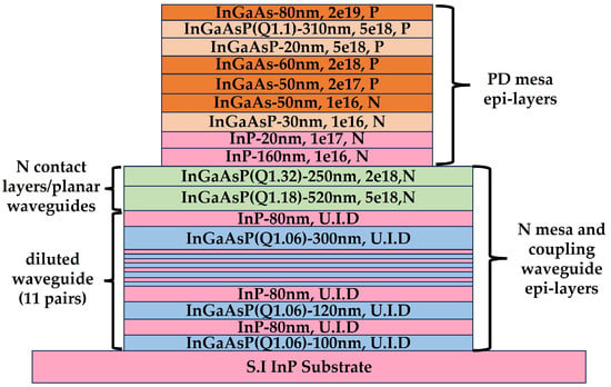
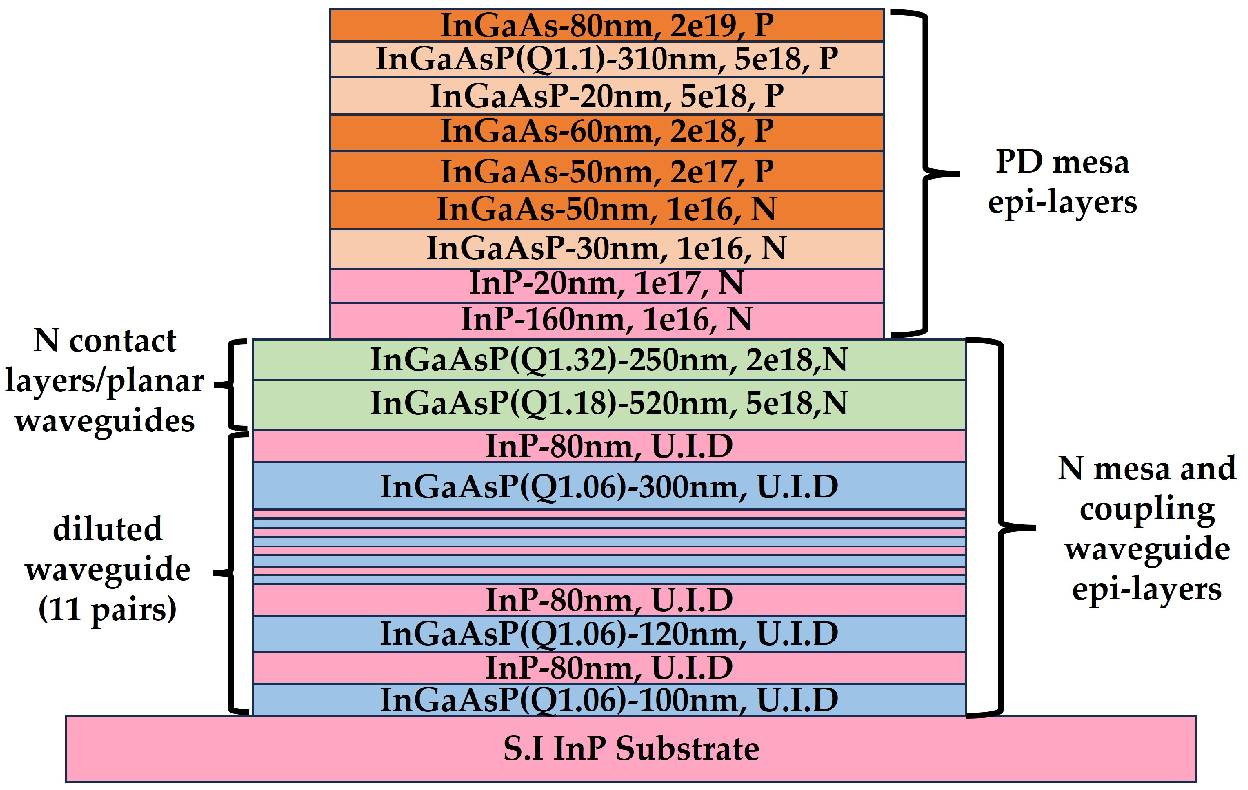
The UTC photodetector is integrated on a 3.85 μm thick coupling waveguide through a single epitaxy growth consisting of a stack of InP/InGaAsP(Q1.06) layer pairs (diluted waveguide) and two planar waveguide layers on top. Each InP layer has a constant thickness of 80 nm, whereas the thickness of InGaAsP(Q1.06) layers increases from 100 nm to 300 nm from bottom to top. The planar waveguide layers are N-doped for N contact and electron collection. Consecutively on the coupling waveguide is a 160 nm collector lightly doped to 1 × 1016 cm−3, a 20 nm cliff layer moderately doped to 1 × 1017 cm−3, a 110 nm absorber of three graded P-doped InGaAs layers, a 310 nm InGaAsP(Q1.1) electron barrier layer, and a P contact InGaAs layer. Two extra InGaAsP bandgap-grading layers of 20 nm and 30 nm are also inserted on the top and bottom of the absorber, respectively. Details of the epi-layers are summarized in Figure 1 below.
Figure 1.
Epi-layer structure of the uni-traveling carrier photodetector.
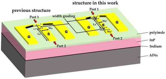
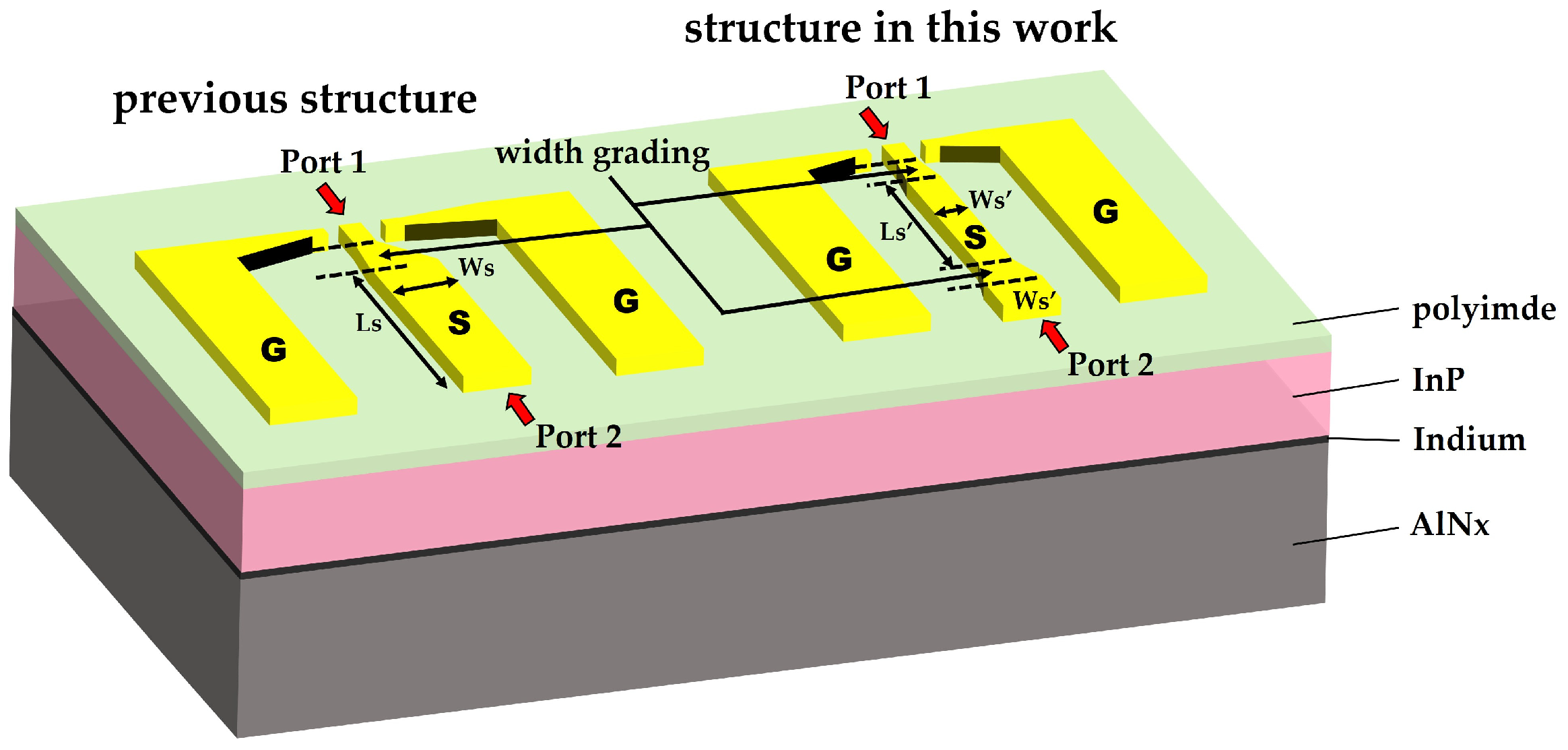
Ground–signal–ground (GSG) on-chip coplanar lines are used to collect photocurrent from the junction, and the parasitic capacitance and inductance of the CPLs will also add to the total impedance seen by the probes or readout circuits. Depicted in Figure 2 are two GSG designs from our previous work and this work. For the signal lines, only a rectangle-shape line with a length of Ls and a width of Ws was used for both signal transmission and pad contact previously. In this work, the signal line is optimized to a transmission region with a length of Ls’ and a width of Ws’, and a region pad of 40 μm × 40 μm, both connected by a width grading region 10 μm long. Another width grading region is designed for signal feed from Port 1 to the signal line, which is 3.5 μm long in this work but 70.5 μm in the previous structure. Ground lines are also narrowed from 98 μm to 60 μm and aligned to the signal line at Port 2. The center-to-center distance of the ground–signal (GS) lines is also reduced to 100 μm from 150 μm to mitigate the RF wave transmission loss and device–probe coupling loss. The dielectric substrate under the gold GSG lines consists of a 3 μm polyimide layer, a 120 μm InP substrate layer, and a 1 μm indium layer on a 1.5 mm AlNx substrate as is the case in reality after chip fabrication.
Figure 2.
Schematic of GSG CPLs.
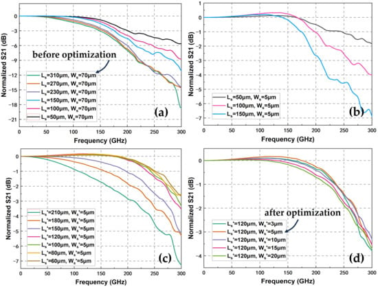
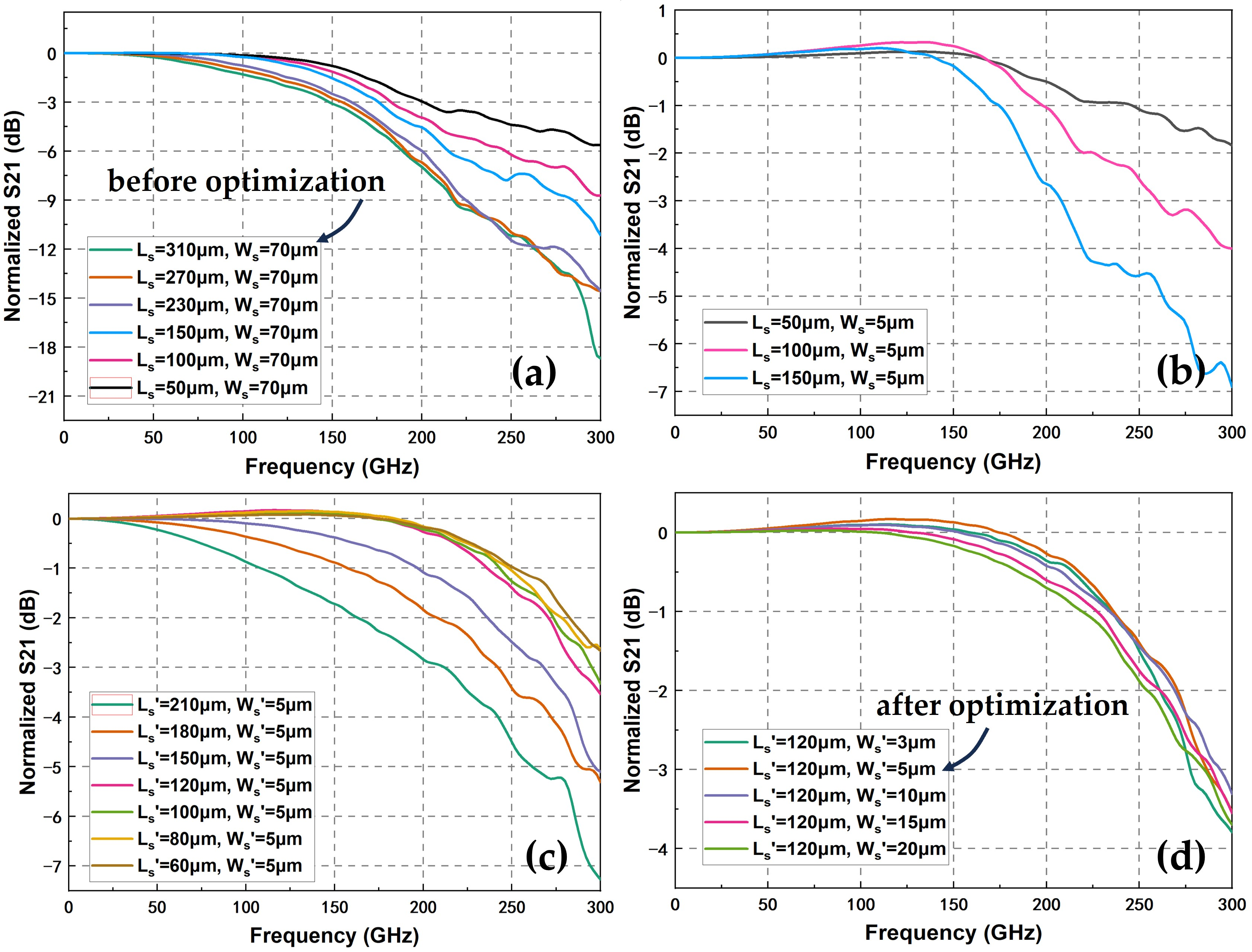
Both GSG CPL structures were simulated for transmission up to 300 GHz by the Finite Element Method, with the maximum mesh size of 1 μm and at least 10 mesh grids at the narrowest line for the highest frequency. Both ports were terminated with 50 Ω impedances. The S21 results are shown in Figure 3. Starting from the CPL size in the previous design as pointed out in Figure 3a, Ls was the first parameter to be swept and simulated. With the reduction in Ls, the normalized S21 curve lifts gradually at high frequency beyond 50 GHz, with a −3 dB bandwidth rising from 150 GHz to 200 GHz. Then, an extreme narrow-down of Ws = 5 μm was introduced for three short Ls situations in Figure 3a, and an uplift in response between 50 GHz and 150 GHz could be achieved in Figure 3b, which is attributed to the inductance of the signal line. With Ws’ also fixed to 5 μm, Ls’ was swept for the new CPL design in Figure 3c. For Ls’ not exceeding 120 μm, the normalized S21 varies little during the whole band, but decreases fast for longer Ls’. This may indicate that the CPL capacitance has overruled the inductance, for the response curves no longer show any uplifts. Also confirmed in Figure 3d is the inductance reliance on the signal width, where only small Ws’ values lead to the uplift of response curves, and nearly no uplift is observed for Ws’ = 20 μm. In comparison, the optimized GSG pattern enables a −3 dB decline at a very high frequency of 280 GHz, whereas the previous GSG introduced loss over 3 dB beyond just 150 GHz. The response enhancement between 50 GHz and 150 GHz will surely help to improve the total PD bandwidth when taking the PD junction into consideration.
Figure 3.
S21 simulation results for both GSG CPLs: (a) previous design with different Ls values, (b) previous design with narrowed signal line and different Ls values, (c) new design with different Ls’ values, and (d) new design with reduced signal line length and different Ws’.
3. Device Fabrication and Measurement
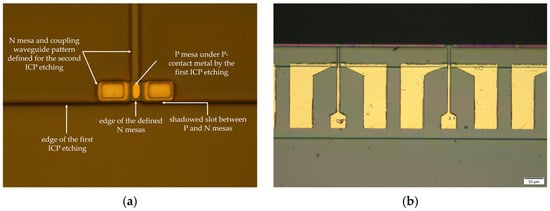
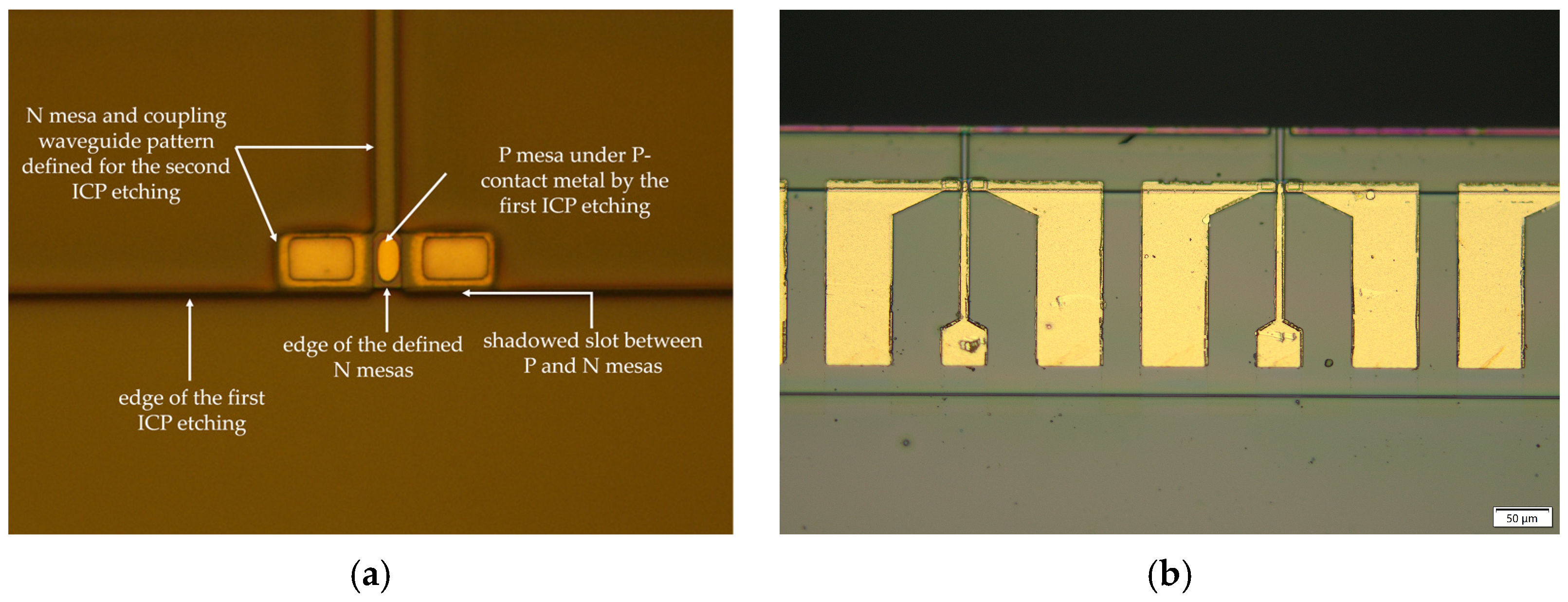
Device fabrication started with the deposition of Pt-Ti-Pt-Au P-contact metal by e-beam evaporation, which was followed by inductively coupled plasma (ICP) etching to define the P mesa position. In this work, we adopted a two-step etching process to form the rectangle P mesa, N mesa, and the coupling waveguide simultaneously, instead of three individual etchings for each region in our previous work. In the first step, only three sidewalls of the P mesa were etched down to the N-contact layer surface, leaving the remaining sidewall intact—otherwise a down-step to the N mesa would have been formed beneath the passivation layer. In the second step, both the N mesa and the coupling waveguide were deeply etched to the substrate, during which the last sidewall of the P mesa was also etched. Consequently, on the side of the P mesa where the signal line transitions from the P mesa top down to the substrate, both the P and N mesas share a common sidewall, thereby avoiding the step that would otherwise be introduced by the overlaying N mesa.
The N-contact metal was sputtered and lifted off between the two etching steps, and a photolithographic polyimide layer was spun and solidified after the deep etching for passivation, leaving P and N contact windows open for CPL deposition. The CPLs were electroplated to 1.8 μm on a 300 nm Ti-Au seed layer by sputtering and lift-off too. The substrate was chemically thinned to 120 μm by hydrochloric acid and phosphoric acid solutions for convenient cleaving. Deep trenches perpendicular to coupling waveguides were formed during deep etching to help locate the cleaving point. After cleaving, the bar chips were deposited with SiO2-Ta2O5 anti-reflection films on the input facets. Pictures of devices in and after fabrication are provided in Figure 4. The actual coupling waveguide length after cleaving is measured to be 43.8 μm.
Figure 4.
Microscope photographs of the fabrication process: (a) after the photolithography of the second ICP etching pattern, and (b) device bar ready for measurement.
The cleaved bars are mounted on Al3N4 heat sink substrates by fused indium, with the device input facets slightly protruding at substrate edges for the convenience of fiber coupling. Photo currents and dark currents were collected using on-chip probes, and the fiber-to-device-facet alignment was ensured by monitoring photocurrents during precise fiber position adjustment.
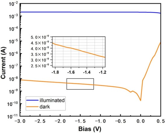
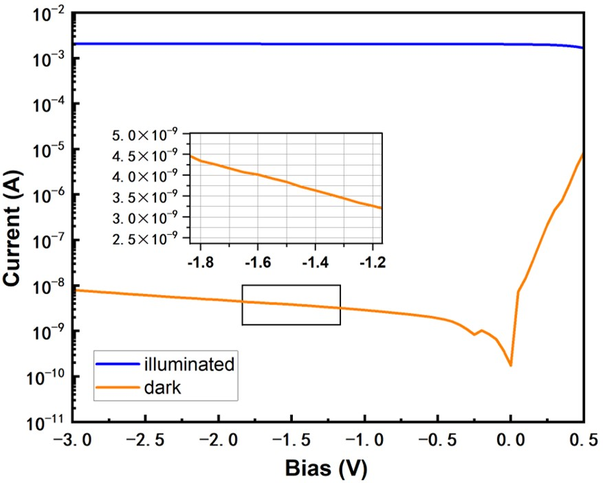
Dark current and photocurrent were measured using a parameter analyzer, where an optical illumination power of 4.33 mW at 1550 nm was measured for the coupling tapered fiber, and the I–V curves are plotted in Figure 5. The dark current remains low under 8.0 nA till −3.0 V, and reads 3.84 nA at −1.5 V where the photodetector was further measured for bandwidth and eye-diagrams. A photocurrent of 2.06 mA was observed at −1.5 V and 2.09 mA at −3.0 V, which amounts to a photoresponsivity of at least 0.476 A/W.
Figure 5.
Dark current and photocurrent measurement results.
The bandwidth of the photodetectors was measured by the combination of a vector network analyzer (VNA) setup and a heterodyne setup where two lasers with identical polarizations were interfered for a high-speed magnitude-modulated optical source. Below 40 GHz, the VNA setup was used with a coaxial GSG probe for photocurrent collection. For frequency over 40 GHz, the RF power meters were used to measure PD output power as the frequency difference between the two lasers swept from 40 GHz to 170 GHz. Three GGB waveguide probes were used to cover the entire bands of 40~50 GHz, 75~110 GHz, and 110~170 GHz, whose insertion losses were carefully assessed from data sheets and de-embedded. All coaxial and waveguide probes feature the same 100 μm GSG pitch.
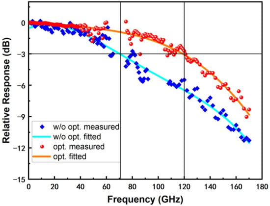
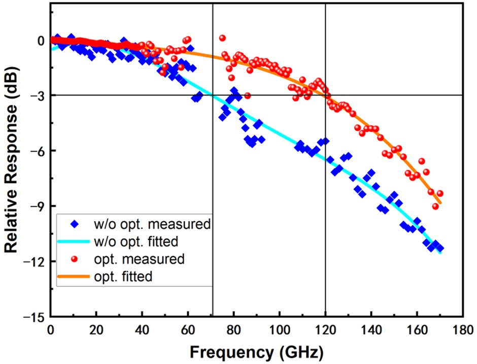
Figure 6 exhibits the measured and fitted results of PD bandwidth for both CPL designs with and without (w/o) optimization (opt.) After CPL optimization, the device achieves a bandwidth of 120 GHz. Under the same active area of 50μm2, this value represents a 69% improvement compared with our previous one that only reaches 71 GHz. For the optimized CPL, the scattered data denoted by red circles manifest some irregular fluctuation beyond 40 GHz, which is also observed in the whole band of scattered data for CPL without optimization denoted by the blue diamonds. The reason should originate from the unstable composite wave magnitude coming from two individual lasers, for the data below 40 GHz of the PD without CPL optimization was also acquired from the heterodyne setup, instead of the VNA setup.
Figure 6.
Bandwidth results at −1.5 V bias centered at 1550 nm and 5.0 mA average photocurrent.
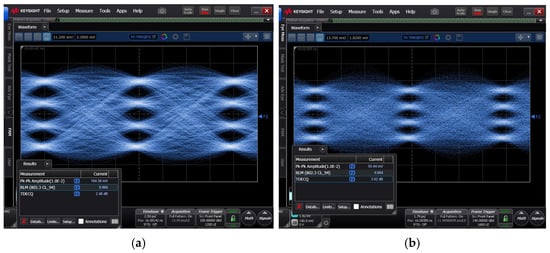
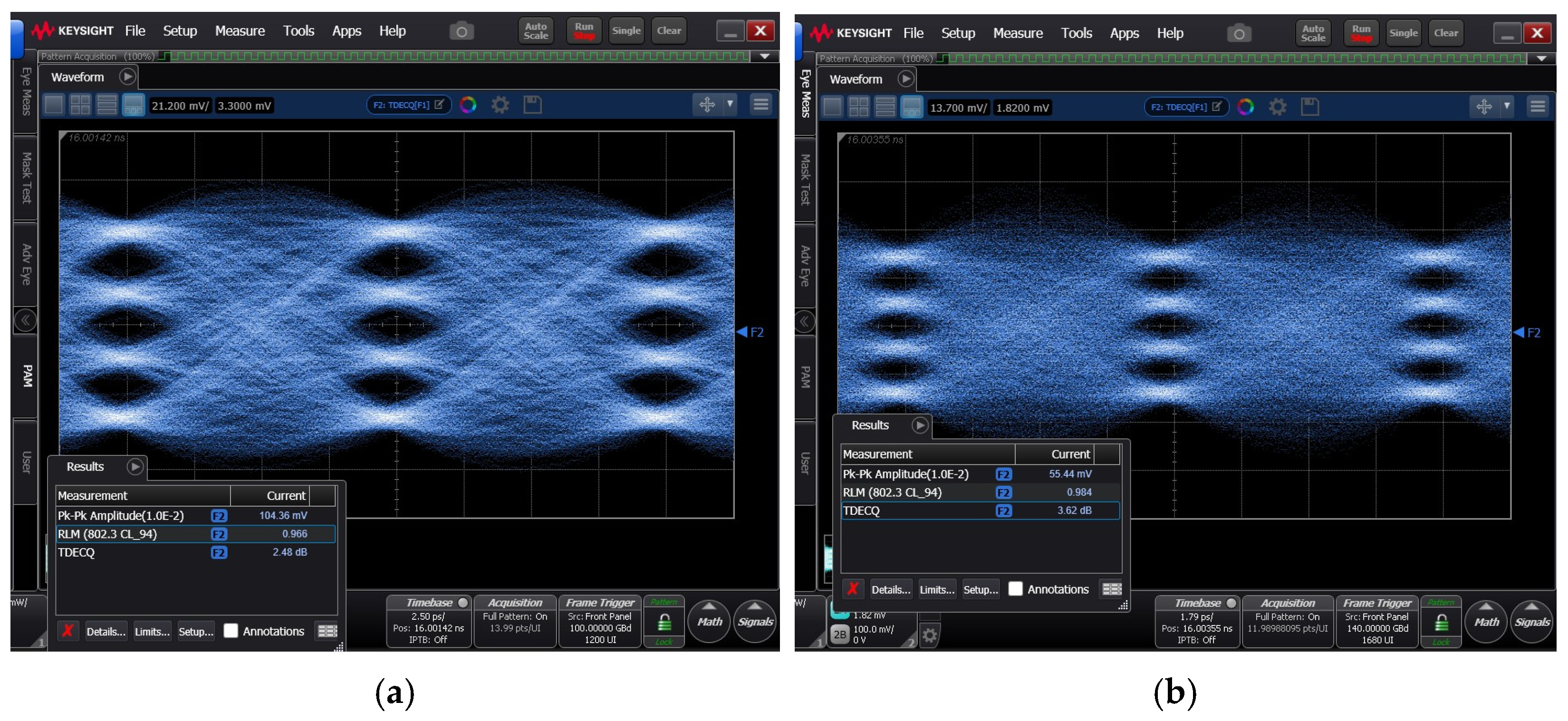
Eye-diagrams were also measured to examine systematic transmission under PAM4 format. Both 100 Gbaud and 140 Gbaud rates were examined with on-chip probes, and the results are shown in Figure 7. The four energy levels are distinct with clear open eye patterns. Though the bit-error-rate (BER) is higher than standards during measurement, the high RMS Level Mismatch (RLM) over 0.96 and low Transmitter and Dispersion Eye Closure Quaternary (TDECQ) less than 3.62 dB still reflect a competitive performance for over 280 Gb/s for PAM4 signals. We believe that the performance could still remain excellent for better BER if higher photocurrents are biased. It should be noted that the frequency response of the 145 GHz bandwidth modulator was also included in the measurement results, and measurement beyond 140 Gbaud was therefore limited and unavailable due to higher response loss.
Figure 7.
PAM4 eye-diagram measurement results: (a) at 100 Gbaud and 4 mA average photocurrent; (b) at 140 Gbaud and 3 mA average photocurrent.
4. Discussion
The measurement results demonstrate an obvious improvement in both photoresponsivity and bandwidth performance. On one hand, the coupling waveguide length adopted in this design is longer, avoiding the situation in our previous work where the minimum optical power was evanescently coupled to the PD absorber due to the varied optical field distribution within the multimode waveguide. On the other hand, the additional anti-reflection film on the end facet also contributes to a reduced coupling loss.
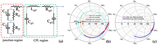
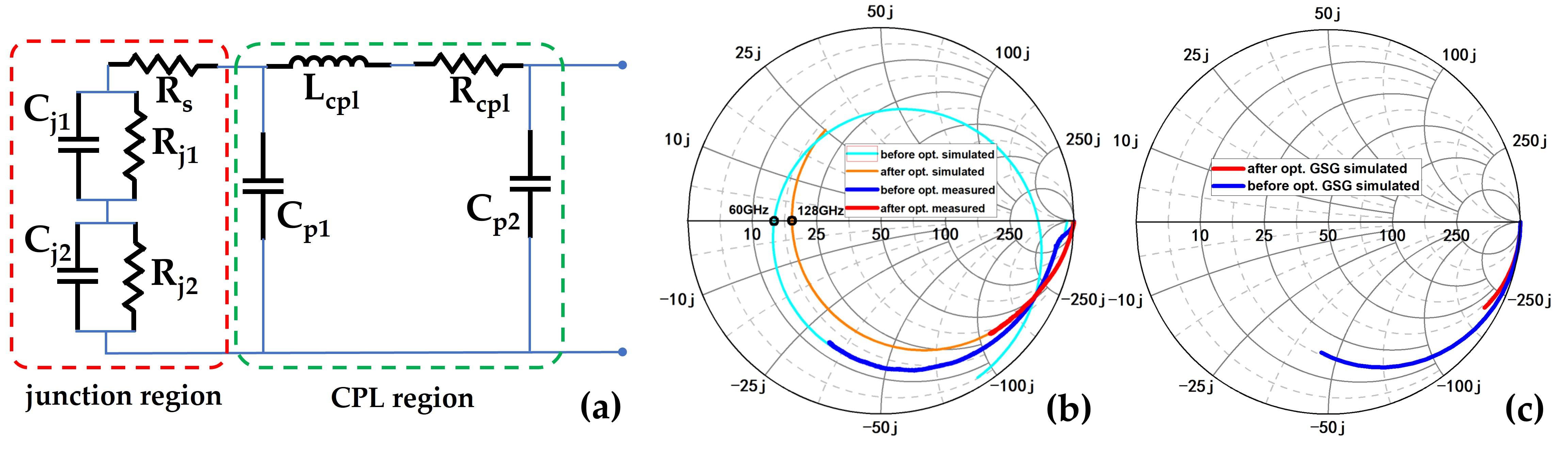
As for the bandwidth improvement, we further conducted circuit simulations to clarify the influence of different CPL designs. The equivalent circuit is shown in Figure 8a to emulate the PD junction (red dashed line region) in series with the CPLs (green dashed line region) seen from the calibrated 50 Ω probe. Parameters were fitted to the measured S22 data in Figure 8b.
Figure 8.
S22 parameter analysis results: (a) the equivalent circuit model; (b) measured (from 1 MHz to 40 GHz) and simulated (from 1 GHz to 170 GHz) S22 results of the PD; (c) simulated S22 results of the CPLs (from 1 MHz to 40 GHz).
The deduced circuit parameters could be used to estimate the PD characteristics. Limited by the VNA capability, only parameters at the relatively low frequency band were fitted out. At high frequencies, the parallel junction resistances Rj1 and Rj2 should gradually increase and be reckoned as an open circuit; therefore, the whole junction capacitance is approximated as:
Cj ≈ (1/Cj1 + 1/Cj2)−1.
In addition, the whole parallel capacitance of the CPLs could be estimated by the sum of Cp1 and Cp2 at high frequency as will be denoted by Cp. Key parameters are summarized in Table 1 below.
Table 1.
Fitting results for the PD.
The equivalent junction capacitances (Cj) deviate less due to the same PD mesa designs for both trials. The smaller value can be attributed to the reduced actual mesa size resulting from the overlaid photolithography and two ICP etchings mentioned in Section 2. The capacitance (Cp), inductance (Lcpl) and resistance (Rcpl) of the CPLs differ remarkably, which reflects the effect of the optimized size. The narrower signal line and the two-step etching process have decreased the capacitances simultaneously as the deduced Cp comprises 34.90 fF for Cp1 and 18.29 fF for Cp2 before optimization and 6.20 fF for Cp1 and 1.09 fF for Cp2 after optimization. For Rcpl, the signal line size variation dominates the resistance change, as calculated by:
where ρ, L, and A represent the resistivity, length and cross-section area of the transmission line respectively. Taking the rectangular portions in both CPLs for a rough estimation where the signal line is in series with two parallel ground lines, the ratios of the total Lao/Aao and Lbo/Abo amount to 14.46 μm−1 and 3.21 μm−1, respectively. This implies a resistance at least 4.5 times higher after optimization, in general agreement with the fitting result.
R = ρL/A,
The inductance is complex considering both self- and mutual parts for CPLs, with the theoretical equations as follows [20]:
where L is the self-inductance of a transmission line with a rectangle cross-section, M is the mutual inductance of two lines with the same length l. W and H are the width and thickness of the line, and D is the distance between the two lines. Intuitively as in our work, line length l is bigger than the sum of W and H, and therefore L should increase with l monotonally. Similarly, M follows the same trend as L for l is over 1.5 times higher than D, and the inverse hyperbolic sine item also takes dominance. In total, the inductance is still higher for the CPLs before optimization.
For comparison, the S22 simulation results of the CPLs are also plotted in Figure 8c by the FEM described in Section 2. Both curves evolve in similar tendency as in Figure 8b and show less capacitive reactance meanwhile due to the absence of the PD junctions. The fitted circuit parameters for the simulated CPLs alone were also deduced by the “CPL region” circuit in Figure 8a, and the results are shown in Table 2. All capacitances and inductances achieve the same level as Table 1 presents, especially for results before optimization. This could also justify the reduced capacitance and inductance of the optimized CPL structure.
Table 2.
Fitting results for the CPLs alone.
The effect of the reduced CPL capacitance and inductance on frequency response tendency is also reflected in the Smith chart, for a faster conversion from capacitive to inductive impedance could be observed for the previous CPL design, which reveals an early electric resonance at lower frequency and the bandwidth is therefore limited. Over the same frequency range of 40 GHz, the impedance evolves slower for the optimized CPL, and the resonance frequency is predicted to be 128 GHz instead of 60 GHz. Consequently, the frequency response curve in Figure 6 rolls down faster after 128 GHz.
5. Conclusions
In this work, an optimized coplanar waveguide GSG line is designed and proved to induce little parasitic effect on the bandwidth performance of an evanescently coupled waveguide uni-traveling carrier photodetector. Measurement and simulation results compared with our previous work show a significantly reduced parallel capacitance to the PD junction for the optimized CPL, and a remarkable rise in bandwidth up to 120 GHz. The CPL parasitic capacitance weighs much less than the junction, and the bandwidth of the CPL itself amounts to 280 GHz, which means a predictable higher PD bandwidth if the junction capacitance could be further reduced. For the device in this work, the active area is 50 μm2, which is twice or even three times those with bandwidths over 200 GHz. If the area is shrunk to the same size, the shrunk junction capacitance may be controlled within 10 fF, in almost equal weight with the optimized CPL, and the PD bandwidth could be raised again. Theoretically, the PD bandwidth is determined by both carrier transit time and resistance–capacitance (RC) circuit response time, where the transit-time limited bandwidth for the epi-structure in our work is estimated to be 310 GHz. For most UTC-PDs designed for high-speed applications and mentioned above, the transit time is usually a less limiting factor, while RC response time takes dominance. Through the simulation results on our previous CPL design, it is found that the CPL itself could achieve high RF loss as the frequency increases, concealing the merit of the small junction area. Therefore, the CPL frequency response should also be taken into consideration alongside the junction itself during device design.
The high bandwidth of the fabricated device also enables clear eye opening in the PAM4 100/140 Gbaud transmission test, indicating a high bitrate at 280 Gb/s. The photoresponsivity of the device achieves 0.476 A/W, with a low dark current of 3.84 nA at the working condition, which reaches the same level as another very recent report from us featuring a 0.49 A/W high responsivity edge-illuminated UTC-PD with only 90 GHz bandwidth [21]. Additionally, considering the habitual practice of pre-emphasis and electrical amplification techniques used in actual optical transceivers, the fabricated device is quite promising for high-speed photodetection over 200 Gb/s/λ, or even higher for 400 Gb/s/λ.
Author Contributions
Device design, simulation and data analysis were performed by H.Y. (Han Ye). Chip fabrication and process design were performed by Q.H., L.G., and H.Y. (Han Ye). The first draft of the manuscript was written by H.Y. (Han Ye). Supervision and manuscript revision were performed by H.Y. (Hua Yang) and H.Y. (Han Ye). All authors have read and agreed to the published version of the manuscript.
Funding
This research was funded by the National Natural Science Foundation of China, grant number 62404219.
Data Availability Statement
The datasets generated during the current study are available from the corresponding authors upon reasonable request.
Acknowledgments
The authors would like to thank Jie Yan and Gong Dou in Wuhan Optical Valley Information Optoelectronics Innovation Center Co., Ltd., for their help in the eye-diagram measurement.
Conflicts of Interest
The authors declare no conflicts of interest.
References
- AI Boom Accelerates Transitions Across the Industry Supply Chain. Available online: https://www.lightcounting.com/newsletter/en/may-2026-optical-vendor-landscape-376 (accessed on 24 July 2024).
- Cui, J.; Wu, C.; Liu, Z.; Deng, Y.; Hao, B.; Zhang, L.M.; Zhang, T.; Wang, Y.X.; Wu, B.; Zhang, C.X.; et al. Real-Time unrepeated Long-Span Field Trial over Deployed 4-Core Fiber Cable Using Commercial 130-Gbaud PCS-16QAM 800 Gb/s OTN Transceivers. Photonics 2025, 12, 319. [Google Scholar] [CrossRef] [Scilit]
- Porto, S.; Sang, F.; Lavrencik, J.; Abolghasem, P.; Rundquist, A.; Macario, J.; Meighan, A.; Ozdemir, C.; Wang, Y.P.; Fu, W.; et al. 1.6 Tb/s Monolithic InP Transmitter PIC with DFB, MZM, and SOA Arrays. In Proceedings of the Optical Fiber Communication Conference, Los Angeles, CA, USA, 15–19 March 2026. [Google Scholar]
- IEEE 802.3 Ethernet Working Group. Available online: https://www.ieee802.org/3/ (accessed on 24 July 2024).
- Shi, Y.; Zhou, D.; Yu, Y.; Zhang, X.L. 80 GHz germanium waveguide photodiode enabled by parasitic parameter engineering. Phot. Res. 2021, 9, 605–609. [Google Scholar] [CrossRef] [Scilit]
- Chen, D.G.; Zhang, H.G.; Liu, M.; Hu, X.; Zhang, Y.G.; Wu, D.Y.; Zhou, P.Q.; Chang, S.Y.; Wang, L.; Xiao, X. 67 GHz light-trapping-structure germanium photodetector supporting 240 Gb/s PAM-4 transmission. Phot. Res. 2022, 10, 2165–2171. [Google Scholar] [CrossRef] [Scilit]
- Wang, X.; Song, J.W.; Yu, F.X.; Yang, F.H.; Chu, W.; Zhao, H.B.; Cai, H.W.; Zheng, X.Z.; Wu, H.; Hu, X. 100 GHz Ultra-thin Germanium Photodetector with 1.05 A/W Responsivity at 1550 nm. In Proceedings of the Optical Fiber Communication Conference, San Francisco, CA, USA, 30 March–3 April 2025. [Google Scholar]
- Lischke, S.; Peczek, A.; Morgan, J.S.; Sun, K.; Steckler, D.; Yamamoto, Y.; Korndorfer, F.; Mai, C.; Marschmeyer, S.; Fraschke, M.; et al. Ultra-fast germanium photodiode with 3-dB bandwidth of 265 GHz. Nat. Photonics 2021, 15, 925–931. [Google Scholar] [CrossRef] [Scilit]
- Ishibashi, T.; Ito, H. Uni-Traveling Carrier Photodiodes: Development and Prospects. IEEE J. Sel. Top. Quantum Electron. 2022, 28, 3803006. [Google Scholar] [CrossRef] [Scilit]
- Li, Q.L.; Sun, K.Y.; Li, K.J.; Yu, Q.H.; Runge, P.; Ebert, W.; Beling, A.; Campbell, J.C. High-Power Evanescently Coupled Waveguide MUTC Photodiode with >105-GHz Bandwidth. J. Light. Technol. 2017, 35, 4752–4757. [Google Scholar] [CrossRef] [Scilit]
- Meng, Q.Q.; Wang, H.; Liu, C.Y.; Guo, X.; Gao, J.J.; Ang, K.S. High-Speed and High-Responsivity InP-Based Uni-Traveling-Carrier Photodiodes. IEEE J. Electron. Devi. 2016, 5, 40–44. [Google Scholar] [CrossRef]
- Chtioui, M.; Enard, A.; Carpentier, D.; Bernard, S.; Rousseau, B.; Lelarge, F.; Pommereau, F.; Achouche, M. High-Performance Uni-Traveling-Carrier Photodiodes with a New Collector Design. IEEE Phot. Technol. Lett. 2008, 20, 1163–1165. [Google Scholar] [CrossRef] [Scilit]
- Han, Y.R.; Tian, Y.X.; Xiong, B.; Sun, C.Z.; Wang, J.; Hao, Z.B.; Han, Y.J.; Wang, L.; Li, H.T.; Gan, L.; et al. Double-cliff-layer uni-traveling-carrier photodiode with high responsivity and ultra-broad bandwidth. Chin. Opt. Lett. 2024, 22, 052501. [Google Scholar] [CrossRef] [Scilit]
- Huang, Y.C.; Chen, N.W.; Wu, Y.K.; Naseem; Shi, J.W. Improvements in the Maximum THz Output Power and Responsivity in Near-Ballistic Uni-Traveling-Carrier Photodiodes with an Undercut Collector. J. Light. Technol. 2024, 42, 2362–2370. [Google Scholar] [CrossRef] [Scilit]
- Sun, M.W.; Xiong, B.; Sun, C.Z.; Hao, Z.B.; Wang, J.; Wang, L.; Han, Y.J.; Li, H.T.; Gan, L.; Luo, Y. Over 220 GHz evanescently coupled MUTC-PDs with enhanced responsivity. Opt. Express 2025, 33, 13864–13873. [Google Scholar] [CrossRef] [Scilit]
- Li, L.Z.; Long, T.Y.; Yang, X.W.; Zhang, Z.Z.; Wang, L.Y.; Wang, J.Y.; Wang, M.X.; Lu, J.J.; Yu, J.J.; Chen, B.L. Modified uni-traveling-carrier photodiodes with 206 GHz bandwidth and 0.81 AW-1 external responsivity. Nat. Photon. 2025, 19, 1301–1308. [Google Scholar] [CrossRef] [Scilit]
- Morgan, J.S.; Tabatabaei, F.; Fatema, T.; Tang, C.W.; Sun, K.Y.; Lau, K.M.; Beiling, A. Bias-Insensitive GaAsSb/InP CC-MUTC Photodiodes for mmWave Generation up to 325 GHz. J. Light. Technol. 2023, 41, 7092–7097. [Google Scholar] [CrossRef] [Scilit]
- Ye, J.H.; Huang, Y.Q.; Yang, M.X.; Tan, S.H.; Ren, X.M. Bias-Free Operational UTC-PD Pair for Optoelectronic Mixing. IEEE Trans. Electron Devices 2025, 72, 2406–2410. [Google Scholar] [CrossRef] [Scilit]
- Ye, H.; Han, Q.; Wang, S.; Geng, L.Y.; Chu, Y.M.; Zheng, Y. Bandwidth enhancement of InP/InGaAs waveguide uni-traveling carrier photodetectors for over 100 GHz bandwidth using impedance lines. Opt. Laser Technol. 2025, 181, 111942. [Google Scholar] [CrossRef] [Scilit]
- Balakrishnan, S.; Park, J.H.; Kim, H.; Lee, Y.M.; Chen, C.P. Linear Time Hierarchical Capacitance Extraction Without Multipole Expansion. In Proceedings of the International Conference on Computer Design, Austin, TX, USA, 23–26 September 2001. [Google Scholar]
- Zheng, Y.; Han, Q.; Ye, H.; Wang, S.; Chu, Y.M.; Geng, L.Y.; An, J.M. High-Responsivity Waveguide UTC Photodetector with 90 GHz Bandwidth for High-Speed Optical Communication. Photonics 2025, 12, 891. [Google Scholar] [CrossRef] [Scilit]

Disclaimer/Publisher’s Note: The statements, opinions and data contained in all publications are solely those of the individual author(s) and contributor(s) and not of MDPI and/or the editor(s). MDPI and/or the editor(s) disclaim responsibility for any injury to people or property resulting from any ideas, methods, instructions or products referred to in the content. |
© 2026 by the authors. Licensee MDPI, Basel, Switzerland. This article is an open access article distributed under the terms and conditions of the Creative Commons Attribution (CC BY) license.