


Abstract
To prevent the collapse of strip waveguides caused by complete undercut during hydrofluoric acid (HF) release in SOI-based cavity optomechanical accelerometers, we propose using rib waveguides as the on-chip optical transmission medium. Based on a 250-nm-thick SOI wafer, we systematically analyze the photonic crystal (PhC) microcavity, rib waveguide transmission, edge coupling, mode conversion to the PhC waveguide, and evanescent coupling. The PhC microcavity has a quality factor of 2.26 × 10⁵ at 1549.15 nm. The optimized rib waveguide (rib width 500 nm, rib height 220 nm) shows a transmission loss of 0.16 dB over 5000 μm. The rib-to-PhC waveguide coupling efficiency is 94.3% (0.25 dB loss), and a 90-μm-long tapered edge coupler achieves 65% efficiency (1.9 dB loss). The total optical path loss (including two edge couplers, rib waveguide transmission, and rib-to-PhC taper) is 4.21 dB. While maintaining optical performance comparable to strip waveguides, the rib waveguide design significantly improves post-release structural integrity at the design level. This work provides a viable optical circuit design foundation for reliable monolithically integrated cavity optomechanical accelerometers, with device fabrication and full system-level characterization planned as future work.
1. Introduction
High-precision acceleration measurement is crucial in fields such as inertial navigation, seismic monitoring, and consumer electronics. Micro-opto-electromechanical system (MOEMS) accelerometers, combining the high sensitivity of optical measurement with the miniaturization capability of microelectromechanical systems, have become a research hotspot [1,2,3]. Cavity optomechanical accelerometers leverage strong coupling between an optical microcavity and a mechanical oscillator, achieving detection precision approaching the thermal noise limit [4,5]. The versatility of cavity optomechanical systems has been further demonstrated in recent years across diverse applications, including PT-symmetric microresonators for significantly enhanced nonlinear optical signal processing with ultra-low pump power [6], ultra-stable phonon lasers with sub-mHz linewidth (0.44 mHz) via closed-loop feedback for precision sensing [7], optomechanical self-oscillation with ultra-narrow linewidth for high-resolution temperature sensing [8], and thermal-locked cascaded fiber microcavities for ultrasensitive acoustic sensing [9]. Currently, cavity optomechanical accelerometers are evolving from discrete devices towards monolithic integration. Achieving efficient and reliable coupling from a laser to the on-chip microcavity is a key challenge. Existing schemes indicate that direct coupling using U-shaped tapered optical fibers [10,11] suffers from insufficient stability, whereas integrated waveguide coupling methods (such as grating couplers or edge couplers [12,13]) are more promising.
However, a frequently overlooked issue is that in traditional MEMS processes using silicon-on-insulator (SOI), the hydrofluoric acid (HF) etching used to release movable structures completely removes the buried oxide layer, causing strip waveguides to lose bottom support and collapse, severely compromising yield [14,15]. Current research mainly focuses on improving coupling efficiency and optomechanical coupling strength, but pays insufficient attention to the reliability issues of transmission structures induced by the release process [16,17].
This paper proposes replacing strip waveguides with rib waveguides to alleviate the process reliability bottleneck. Rib waveguides retain a thin slab layer after etching. The underlying silicon dioxide layer is not etched during the HF process, thus effectively avoiding waveguide collapse. Since the mode field distribution of rib waveguides differs from that of strip waveguides, their optical performance needs re-optimization, necessitating redesign of processes including edge coupling efficiency and mode conversion.
Based on an SOI wafer with a 250 nm thick top silicon layer, this study presents a systematic design scheme for a rib waveguide integrated optical path. The resonant mode and band structure characteristics of the PhC microcavity have been reported in detail in previous strip waveguide integration studies [18]; here we only present key parameters and results. The focus is on re-optimizing the transmission characteristics of the rib waveguide, edge coupling, and rib waveguide to PhC waveguide coupling, providing an updated loss budget. This work lays the design foundation for achieving high-reliability, high-precision monolithically integrated cavity optomechanical accelerometers. The scope of this paper is limited to the optical path design and simulation; device fabrication, HF release validation, and complete system level sensing performance evaluation (including noise equivalent acceleration and bandwidth) constitute our ongoing and future work.
2. Device Architecture and Operating Principle
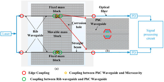
Figure 1a shows the overall architecture of the proposed rib waveguide-integrated cavity optomechanical accelerometer. The device is built on a silicon-on-insulator (SOI) wafer with a top silicon layer thickness of 250 nm, a buried oxide layer thickness of 3 μm, and a substrate thickness of 700 μm. The device comprises the following core functional units: The mechanical sensing module employs a straight-beam resonant structure consisting of a fixed mass and a movable mass to detect external acceleration. The optomechanical transducer module contains two adjacent PhC slabs embedded in the adjacent edges of the fixed and movable masses, with a 100 nm air gap between the two slabs. By precisely adjusting the displacement of air holes (green, blue, and red arrows in Figure 1b represent displacements of 15 nm, 10 nm, and 5 nm, respectively, all directed towards the air gap), a defect microcavity is formed. The optical transmission network employs rib waveguides with a rib width of 500 nm and a slab thickness of 30 nm. The optical coupling path consists of a three-stage link: edge coupling between a tapered lensed fiber and the rib waveguide, tapered mode conversion between the rib waveguide and the PhC waveguide, and evanescent wave coupling between the PhC waveguide and the microcavity. It should be noted that the rib waveguides are routed on the fixed mass portion of the device; the movable mass and suspension beams are unaffected by the rib-waveguide architecture. Therefore, the mechanical stiffness and mass distribution of the sensing structure remain unchanged.
Figure 1.
(a) Schematic of the overall structure of the rib waveguide-integrated accelerometer; (b) Detail of the PhC microcavity.
The device operates as follows: Light from a distributed feedback (DFB) laser first couples into the rib waveguide via edge coupling, then enters the PhC waveguide through a tapered mode conversion region, and finally couples into the microcavity, establishing a stable resonant optical field. When an external acceleration acts on the device, the movable mass displaces, changing the air gap between the two PhC slabs, thereby causing a shift in the microcavity resonance wavelength, which modulates the intensity of the output optical signal. A photodetector captures the output optical signal, and a signal processing circuit performs demodulation and analysis to ultimately obtain a high-precision measurement of acceleration.
The optical path design plays a critical role in determining the accelerometer readout capability. The total optical transmission loss determines the optical power available at the photodetector, which directly affects the signal-to-noise ratio. The PhC microcavity Q-factor determines the resonance lineshape and thus the transduction efficiency from mechanical displacement to optical intensity modulation. In addition, the structural integrity provided by the rib waveguide architecture ensures long-term stability of the optical path.
To assess the reliability improvement offered by the rib waveguide architecture, we first establish a baseline by examining the strip waveguide configuration. The strip waveguide spans approximately 5000 μm from the PhC microcavity to the chip edges (about 2500 μm on each side), which is determined by the chip width required for the end-polishing fixture used in optical facet preparation. This length includes a 220-μm-long PhC waveguide section. The waveguide is flanked by air slots that serve as HF release windows, allowing complete removal of the underlying BOX layer and thus forming a fully suspended structure. In contrast, the rib waveguides in our proposed design are anchored in the fixed region, separated from the movable structures, where no air slots are present, so the underlying BOX layer remains intact during HF release.
To provide quantitative insight into the structural reliability advantage of the rib waveguide architecture, we perform a theoretical comparison based on Euler–Bernoulli beam theory [19]. For a fully undercut strip waveguide, the structure behaves as a cantilever beam with a critical buckling load:
where E is Young’s modulus of silicon (169 GPa for the ⟨110⟩ orientation commonly used in SOI devices), I = w3t/12 is the area moment of inertia (w = 500 nm width, t = 250 nm thickness), and L is the beam span. For a representative short beam span of L = 200 μm, the critical compressive stress for buckling is approximately 217 kPa (corresponding to a critical load of 2.715 × 10⁻⁸ N). When extended to the actual suspended waveguide length in our device (L = 5000 μm), the critical stress decreases to approximately 347 Pa (corresponding to a critical load of 4.344 × 10⁻¹¹ N). Both values are orders of magnitude lower than typical residual stress levels in SOI wafers, which are on the order of MPa (e.g., approximately 25–47 MPa have been reported in commercial SOI wafers). This quantitatively confirms that a fully suspended strip waveguide would inevitably buckle under residual stress during release. In contrast, the rib waveguide, attached to the unetched buried oxide, forms a composite structure with the underlying SiO2 layer and silicon substrate. The stress is therefore distributed across the entire stack cross-section rather than being borne solely by the suspended silicon membrane, resulting in an equivalent flexural rigidity that is several orders of magnitude higher than that of the suspended silicon beam. This analysis provides quantitative theoretical support for the design-level reliability advantage of the rib waveguide architecture.
3. Optical Path Design and Simulation
3.1. Characteristics of the PhC Microcavity
The microcavity structure is identical to that in the strip waveguide scheme of reference [18]: a triangular lattice with lattice constant a = 500 nm, air hole radius r = 187.5 nm, and air slot width w = 100 nm. According to the simulations in that reference, the fundamental resonant mode wavelength is 1549.15 nm and the quality factor is 2.26 × 10⁵. It should be noted that this Q-factor is obtained from ideal 2D FDTD simulations assuming perfectly smooth sidewalls and nominal geometric parameters; sidewall roughness and fabrication-induced dimensional variations are not included. This ideal value serves as a baseline for comparing the optical performance of the rib-waveguide integration scheme against the strip-waveguide design, which used the identical cavity geometry under the same simulation conditions. A detailed tolerance analysis accounting for fabrication variations will be addressed in future work. The plane-wave expansion band structure analysis shows that the TE-mode photonic bandgap ranges from 137.87 to 218.04 THz (the resonant mode profile and TE band diagram, where the red dashed line indicates the light cone boundary, are presented in Figure 2 of that work, to which the reader is referred for further details).
Figure 2.
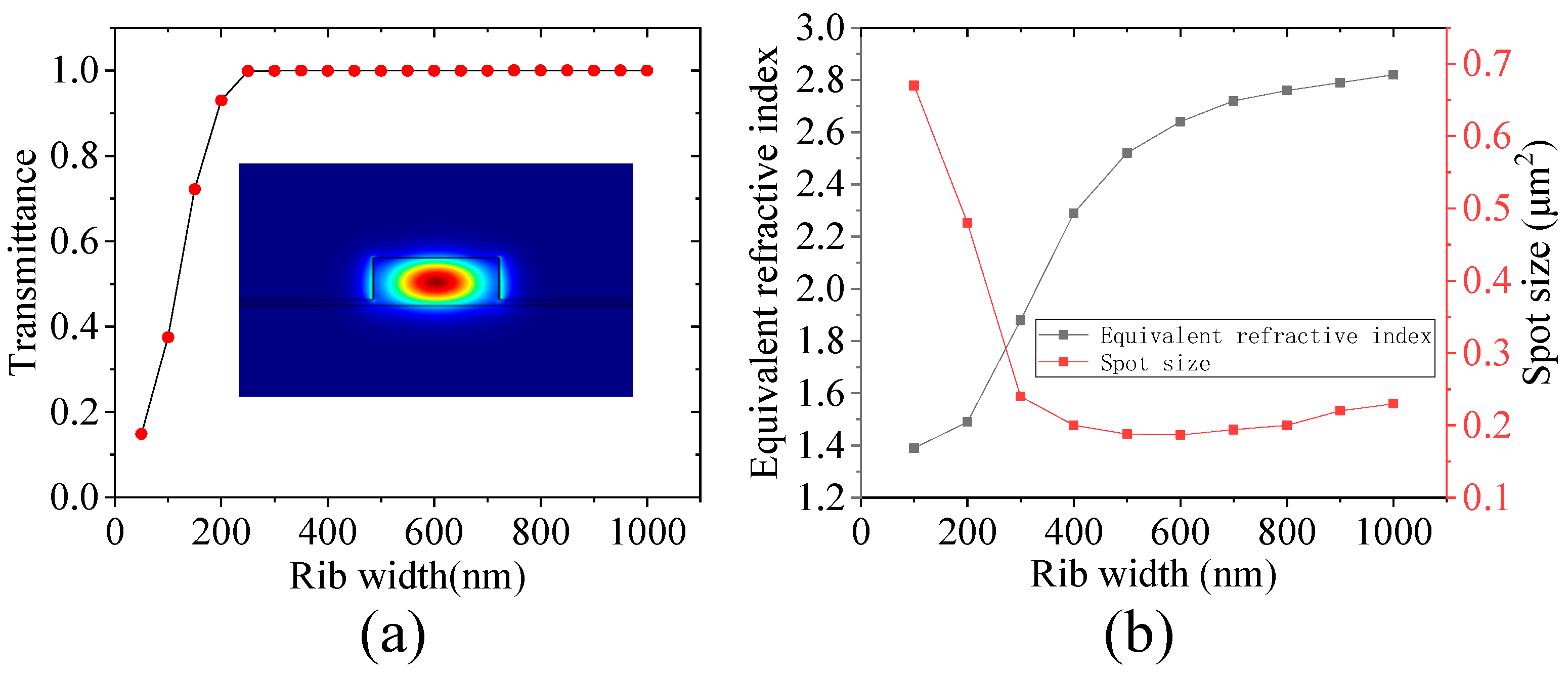
(a) Transmittance versus rib width; (b) Effective refractive index and mode area versus rib width.
3.2. Transmission Characteristics of the Rib Waveguide
The geometric parameters of the rib waveguide are defined as follows: total top silicon thickness 250 nm, rib height 220 nm, slab thickness 30 nm, and rib width to be optimized. The slab thickness of 30 nm is determined by the 250 nm top silicon layer minus the 220 nm rib height. This value falls within the 20–40 nm range that satisfies both the single-mode condition for SOI rib waveguides and the mechanical robustness required to prevent collapse after HF release, as verified by our simulations and consistent with Refs. [10,11]. Figure 2a shows the transmittance of a 100 μm long rib waveguide as a function of rib width at the wavelength of 1549.15 nm. Simulation results indicate that as the rib width increases from 50 nm to 300 nm, the transmittance rapidly rises and exceeds 99.9%, after which it saturates. Considering both single-mode transmission conditions (TE fundamental mode, rib width not exceeding 600 nm) and optimal transmission efficiency, the rib width is finally set to 500 nm. The electric field distribution of the TE fundamental mode in the rib waveguide is shown in the inset of Figure 2a, indicating that the optical field is effectively confined in the rib region.
Figure 2b shows the effective refractive index and mode area as functions of rib width. As the rib width increases from 100 nm to 600 nm, the effective refractive index gradually rises from approximately 2.38 to 2.60. The mode area initially decreases rapidly and then saturates. When the rib width is about 350 nm, the mode area is about 0.35 μm2; when the rib width increases to 500 nm, the mode area decreases to 0.18 μm2; further increasing the rib width has little effect on the mode area. A rib width of 500 nm maintains single-mode transmission while achieving a small mode area, and this mode area matches well with that of the subsequent PhC waveguide, facilitating low coupling loss. For the optimized rib waveguide with 500 nm width, the loss over a 5000 μm transmission length is 0.16 dB (corresponding to a transmittance of approximately 96.4%). We also consider the impact of sidewall roughness on propagation loss in the rib waveguide. The roughness scattering loss can be estimated using the Payne–Lacey model, which relates loss to the sidewall roughness amplitude (σ) and correlation length (Lc). For typical SOI fabrication processes, σ ≈ 5 nm and Lc ≈ 50 nm. Using the mode confinement factor in the rib region (Γ ≈ 85%), the estimated scattering loss at 1550 nm is approximately 1.2 dB/cm for our optimized rib width of 500 nm. This is comparable to values reported for strip waveguides (1.0–1.5 dB/cm) fabricated on similar SOI platforms [10,13]. For a 5000 μm propagation length, this corresponds to 0.6 dB. It should be noted that the Payne–Lacey model provides an upper-bound estimate of the scattering loss; our simulated transmission loss of 0.16 dB does not account for sidewall roughness, representing an ideal scenario. The actual loss would depend on the fabrication quality and is expected to fall between these values. This remains within acceptable limits for on-chip optical interconnect applications. For comparison, under the same simulation conditions, the strip waveguide loss is about 0.2 dB, which is comparable.
3.3. Edge Coupling
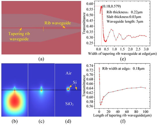
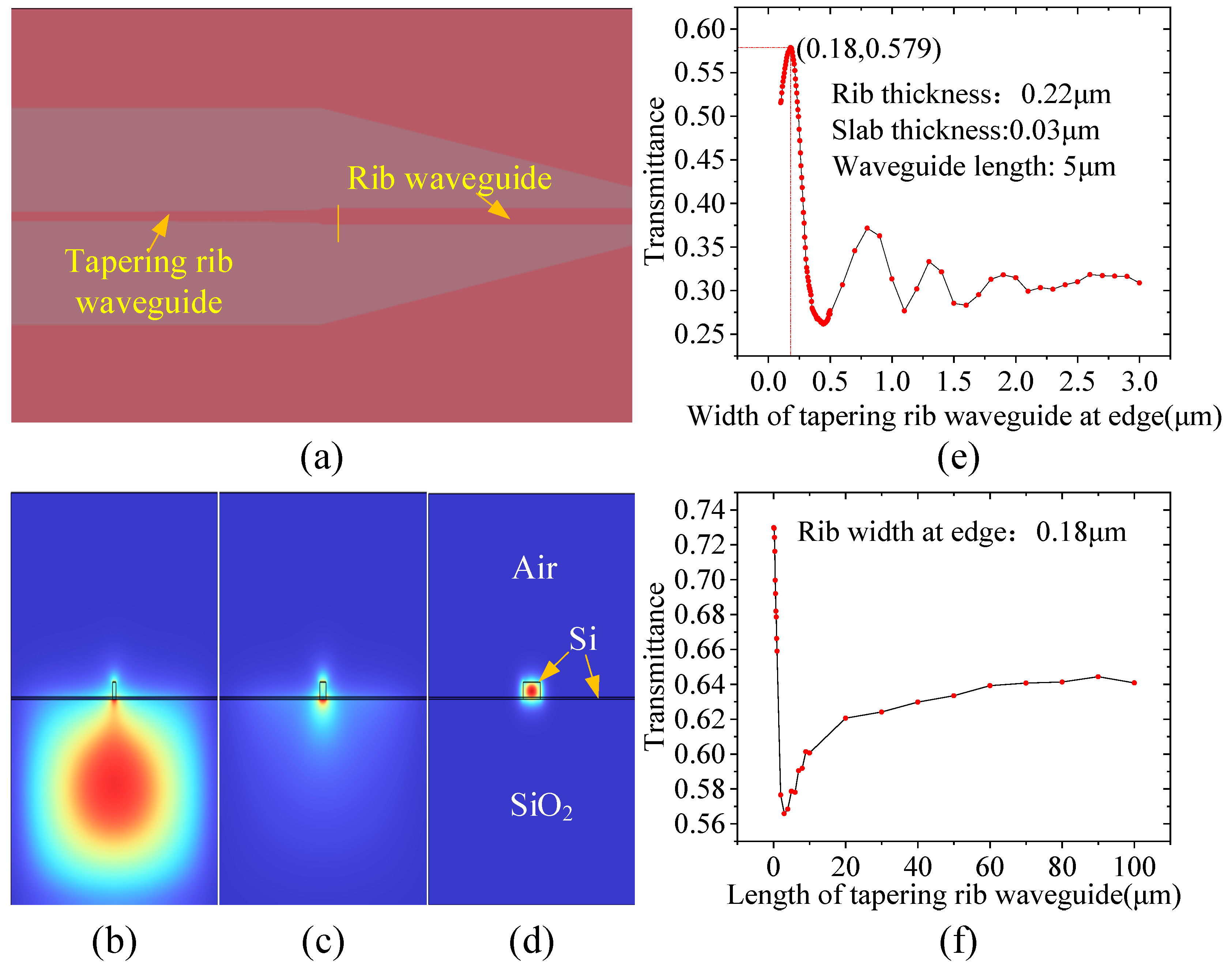
The mode field diameter of a tapered lensed fiber is about 2–3 μm, while the facet size of the rib waveguide is only 500 nm (width) × 250 nm (height), resulting in a significant mode field mismatch. Furthermore, the asymmetric cladding structure of the device (upper cladding: air, lower cladding: SiO2) causes mode field distortion and shifts it towards the substrate. To address these issues, this paper employs an inverse tapered edge coupler [20], as shown in Figure 3a. This coupler starts from a narrow tip and adiabatically expands the mode field to ultimately achieve mode matching with the lensed fiber.
Figure 3.
(a) Schematic of the edge coupler structure; (b) Mode field distribution at a tip width of 0.1 μm; (c) Mode field distribution at a tip width of 0.18 μm; (d) Mode field distribution at a tip width of 0.5 μm; (e) Transmittance versus tip width; (f) Transmittance versus taper length.
Figure 3b–d show the mode field distributions at different tip widths, clearly illustrating the mode evolution process. When the tip width is 0.1 μm (Figure 3b), the optical field is mainly confined within the buried oxide layer (SiO2) beneath the top silicon, with the spot located inside the substrate. When the tip width increases to 0.18 μm (Figure 3c), the mode field moves upward and becomes localized at the rib waveguide facet, with the spot size approaching that of the lensed fiber. When the width reaches 0.5 μm (Figure 3d), the mode field exhibits good single-mode characteristics.
Parameter sweeps yield the transmittance as a function of tip width and taper length, as shown in Figure 3e,f. Figure 3e presents simulation results for an edge coupler with a length of 5 μm, indicating that the optimal transmittance occurs at a tip width of 0.18 μm. Figure 3f shows the transmittance as a function of taper length with the tip width fixed at 0.18 μm: as the taper length increases from 0.1 μm to 3 μm, the transmittance drops significantly from 0.73 to 0.56; as the taper length increases from 3 μm to 100 μm, the transmittance gradually rises and tends to saturate, reaching a maximum value of 0.65 at 90 μm. We also verified convergence by simulating taper lengths up to 120 μm; the transmittance remained essentially flat (variation < 0.5%) between 90 μm and 120 μm, confirming that 90 μm is sufficient for adiabatic mode expansion and that further lengthening yields no significant improvement. The saturation is attributed to the trade-off between improved adiabaticity and accumulated propagation loss in the extended taper region. Considering factors such as process feasibility, chip area, and risk of facet polishing damage, this paper ultimately selects a taper length of 90 μm. At the wavelength of 1549.15 nm, the insertion loss of this coupler is 1.9 dB, corresponding to a transmittance of about 65%. Compared with the strip waveguide structure (optimal taper length 30 μm, loss about 2.2 dB), the edge coupler for the rib waveguide requires a longer optimal taper length and exhibits slightly lower loss. This is because the retained slab layer in the rib waveguide facilitates adiabatic mode expansion, and the longer tapered region provides greater tolerance to facet polishing damage, thus improving yield in actual wafer manufacturing.
Compared with grating-coupler-based fiber-to-chip coupling, which typically suffers from higher insertion loss and limited optical bandwidth [21], our inverse-tapered edge coupler achieves a coupling loss of 1.9 dB with broad bandwidth and polarization insensitivity.
3.4. Coupling Between the Rib Waveguide and the PhC Waveguide
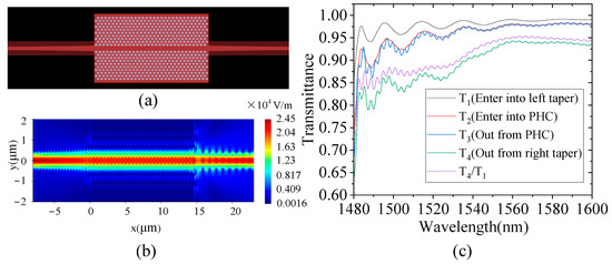
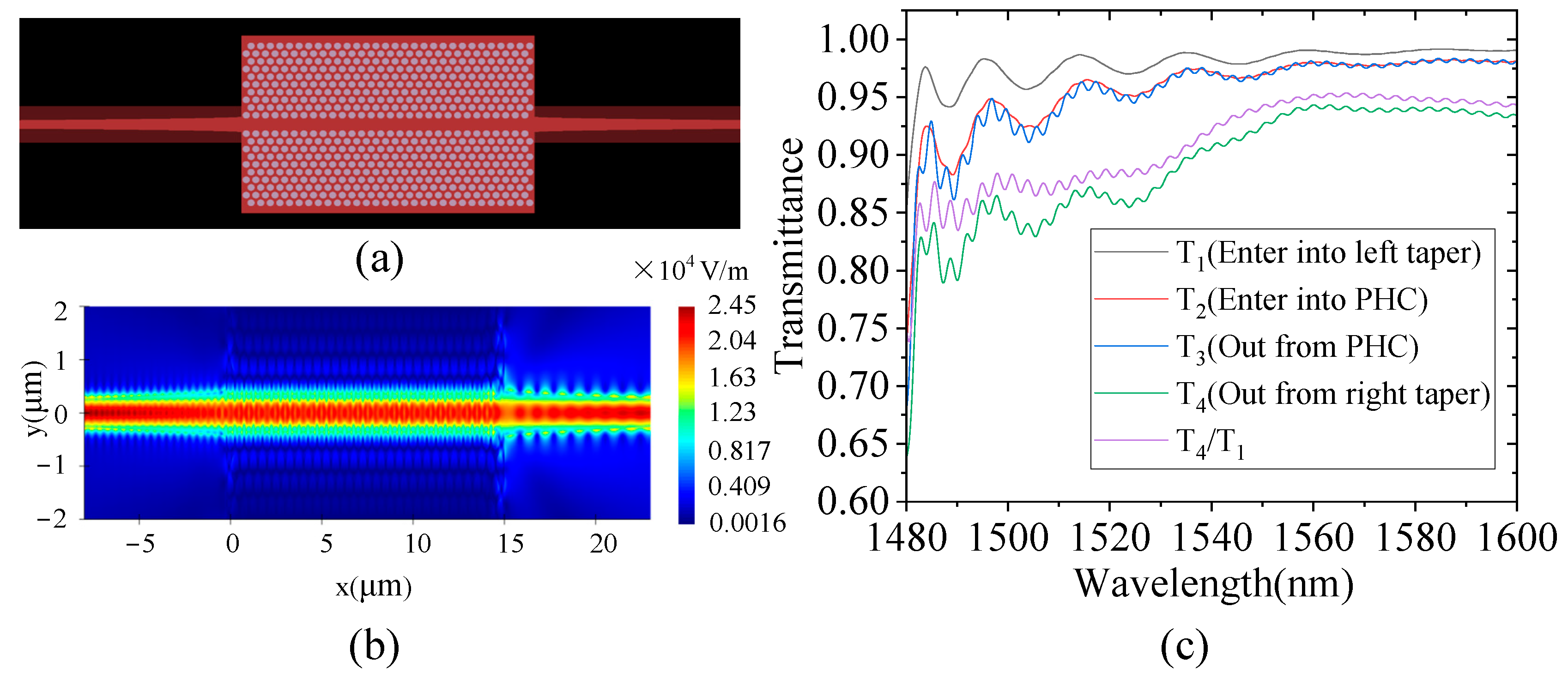
The width of the rib waveguide is 500 nm, while the connected PhC waveguide (formed by removing a row of air holes) has a width of approximately 880 nm, resulting in a significant width mismatch. Direct connection would lead to severe mode mismatch and reflection loss. Therefore, this paper employs a parabolic tapered transition structure with a length of 20 μm to achieve adiabatic mode conversion between them.
The inter-waveguide coupling is simulated and analyzed using the FDTD method; the simulation model is shown in Figure 4a. Figure 4b shows the steady-state electric field distribution at the wavelength of 1549.15 nm: the optical field starts from the left rib waveguide, gradually expands through the tapered structure into the PhC waveguide, and then is guided out to another rib waveguide section through the right symmetric tapered structure. The entire mode conversion process exhibits adiabatic characteristics, with no observable reflection or radiation loss. Figure 4c shows the transmission spectrum. At the wavelength of 1549.15 nm, the transmittance is 94.3%, corresponding to an insertion loss of 0.25 dB. To further quantify the loss contributions of the rib-to-PhC taper, we analyze the back-reflection and out-of-plane scattering losses using additional power monitors in the FDTD simulation. A power monitor placed before the taper input records the reflected power, yielding a back-reflection loss of approximately 0.08 dB (reflectivity < 2%) at the fundamental resonant wavelength of 1549.15 nm. This low back-reflection is attributed to the adiabatic profile of the parabolic taper, which gradually transforms the mode from the rib waveguide to the PhC waveguide with minimal index mismatch. Out-of-plane scattering loss is evaluated by integrating the Poynting vector flux through monitors placed above and below the taper region. The integrated radiation power corresponds to an out-of-plane scattering loss of approximately 0.05 dB, which is negligible compared to other loss contributions (edge coupling: 1.9 dB, waveguide transmission: 0.16 dB, and taper coupling: 0.25 dB). These results confirm that the taper design is well optimized for high-Q cavity excitation.
Figure 4.
(a) Simulation model of the tapered coupling structure; (b) Steady-state electric field distribution at the fundamental resonant wavelength; (c) Transmission spectrum.
The spectrum also reveals that the transmittance (T4/T1) remains between approximately 0.85 and 0.95 across the entire 1480–1590 nm band, corresponding to an insertion loss variation of about 0.23 dB. No 3-dB roll-off is observed within this range, confirming that the taper is broadband and introduces negligible wavelength-dependent loss; its usable bandwidth is therefore limited only by the PhC microcavity resonance rather than by the taper structure itself. Compared with the strip waveguide structure (insertion loss 0.4 dB), the rib waveguide achieves slightly higher coupling efficiency, attributed to the slab-layer-assisted adiabatic mode expansion that reduces radiation loss during mode conversion. The rib-to-PhC coupling efficiency of 94.3% (0.25 dB loss) is competitive with PhC-waveguide-to-fiber coupling efficiencies reported in the literature (e.g., a lower bound of 94% from an optical fiber taper to a PhC waveguide [10]), while our approach avoids the mechanical instability and alignment sensitivity associated with external fiber-taper positioning.
3.5. Evanescent Wave Coupling Between the PhC Waveguide and the Microcavity
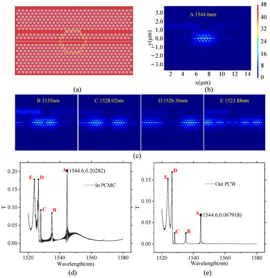
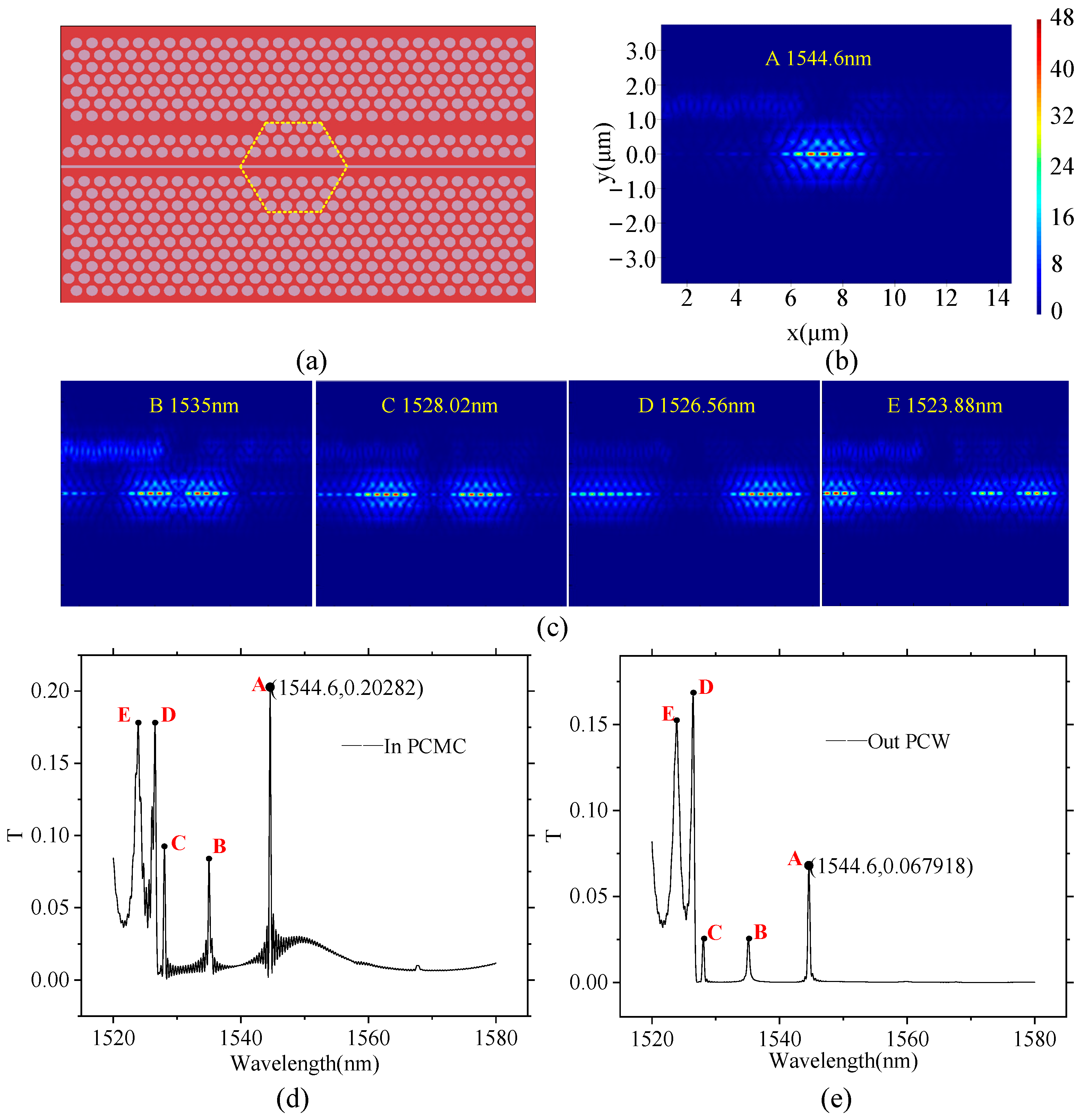
Figure 5a illustrates the coupling structure: a PhC waveguide is formed by selectively removing air holes in the third row above the air slot, while retaining four critical holes within the yellow hexagonal region (i.e., the waveguide is blocked in the middle), forcing light to couple evanescently into the microcavity only laterally, and then symmetrically out to the right waveguide. This configuration is identical to that used in our previous strip waveguide work.
Figure 5.
(a) Model of the coupling structure; (b) Fundamental mode field distribution; (c) Other resonant modes; (d) Transmission from left PhC waveguide into the microcavity; (e) Total transmission from left to right PhC waveguide.
The transmission spectra (Figure 5d,e) exhibit five resonance peaks (A–E). Mode A at 1544.6 nm deviates slightly from the isolated microcavity wavelength of 1549.15 nm due to waveguide loading effects, has an electric field enhancement factor exceeding 40, and represents the fundamental mode (Figure 5b). The other modes are higher-order or parasitic modes (Figure 5c).
Figure 5d shows the normalized transmission spectrum detected by an internal monitor inside the microcavity, with a peak value of 20.28% at the wavelength of mode A, representing the transmittance from the left PhC waveguide into the microcavity (i.e., the ratio of power coupled into the microcavity to the input power). Figure 5e shows the total transmission spectrum from the left waveguide input to the right waveguide output, with a peak value of 6.79% at the same wavelength, corresponding to the total transmittance (power transmission ratio through the complete “input → microcavity → output” link). It should be noted that this coupling process pertains to the excitation and readout of the sensor sensitive element; its power distribution is not included in the total optical path transmission loss discussed below, which only accounts for edge coupling, rib waveguide transmission, and rib-to-PhC tapered coupling.
Compared with fiber-based coupling schemes that rely on tapered optical fibers positioned near the PhC microcavity [22], or phase-matched microfiber-to-cavity coupling [23], our on-chip PhC-waveguide-to-microcavity evanescent coupling provides a fully integrated interface, eliminating the need for external fiber positioning and alignment, and ensuring mechanical robustness essential for accelerometer applications.
4. Conclusions
This study addresses the structural failure issue encountered by cavity optomechanical accelerometers during HF release through the design of a monolithically integrated optical path employing rib waveguides. The optimized rib waveguide (rib width 500 nm, slab thickness 30 nm) exhibits a transmission loss of 0.16 dB over a 5000 μm length, which is comparable to and acceptable versus the ideal simulation value for a strip waveguide (approximately 0.2 dB), confirming that the rib architecture maintains optical performance while offering superior structural integrity. The 90 μm long inverse tapered edge coupler achieves a coupling loss of 1.9 dB, outperforming the strip waveguide scheme (30 μm length, 2.2 dB). The interconnection between the rib waveguide and the PhC waveguide via a 20 μm taper achieves a transmittance of 94.3% (0.25 dB loss). The total loss of the aforementioned optical path (including both edge couplers, rib waveguide transmission, and rib-to-PhC tapered coupling) is 4.21 dB.
Regarding the lateral coupling between the PhC waveguide and the microcavity, because the waveguide is blocked, light can only enter and exit the microcavity via evanescent waves. Simulations yield: the transmittance from the left PhC waveguide into the microcavity is 20.28%, and the total transmittance from the left PhC waveguide through the microcavity to the right waveguide is 6.79%. This coupling process pertains to the excitation and readout of the sensor sensitive element; its power distribution is not included in the aforementioned total optical path transmission loss.
This paper provides a viable optical circuit design for high-reliability, high-precision monolithically integrated cavity optomechanical accelerometers. Future work includes device fabrication, HF release process validation, experimental optical characterization, complete system-level performance evaluation, and detailed structural mechanics analysis (e.g., residual stress distribution and mechanical stability assessment) to quantitatively validate the structural reliability improvement. Practical challenges such as temperature cross-sensitivity, vacuum packaging, and the fundamental thermal noise limit will also be addressed in subsequent experimental studies.
Author Contributions
Conceptualization, C.X.; Methodology, P.K., C.W. and C.X.; Software, P.K. and Y.Z.; Validation, C.W., N.F. and R.Z.; Formal analysis, P.K. and N.F.; Investigation, P.K.; Resources, G.W. and Y.H.; Data curation, R.Z.; Writing—original draft, P.K.; Writing—review & editing, C.W., C.X., N.F., Y.Z., R.Z., G.W. and Y.H.; Visualization, P.K. and Y.Z.; Supervision, C.X. and G.W.; Project administration, C.X.; Funding acquisition, C.X. and Y.H. All authors have read and agreed to the published version of the manuscript.
Funding
This work was supported in part by the National Natural Science Foundation of China (Grant No. 62371106, U2230206, U2441217, and 62204264), in part by Sichuan Provincial Science and Technology Planning Program (Grant No. 2023YFG0040), and in part by Innovation Ability Construction Project for Sichuan Provincial Engineering Research Center of Communication Technology for Intelligent IoT (2303-510109-04-03-318020).
Data Availability Statement
The data presented in this study are available from the corresponding author upon reasonable request.
Conflicts of Interest
The authors declare no conflict of interest.
References
- Sheikhaleh, A.; Abedi, K.; Jafari, K.; Gholamzadeh, R. Micro-optoelectromechanical systems accelerometer based on intensity modulation using a one-dimensional photonic crystal. Appl. Opt. 2016, 55, 8993–8999. [Google Scholar] [CrossRef] [Scilit] [PubMed]
- Lu, Q.; Bai, J.; Wang, K.; He, S. Design, optimization, and realization of a high-performance MOEMS accelerometer from a double-device-layer SOI wafer. J. Microelectromech. Syst. 2017, 26, 859–869. [Google Scholar] [CrossRef] [Scilit]
- Nie, Y.; Huang, K.; Yang, J.; Cao, L.; Cheng, L.; Wang, Q.; Tian, H.; Peihua, W.; Heng, L. A proposal to enhance high-frequency optical MEMS accelerometer sensitivity based on a one-dimensional photonic crystal wavelength modulation system. IEEE Sens. J. 2020, 20, 14639–14645. [Google Scholar] [CrossRef] [Scilit]
- Krause, A.G.; Winger, M.; Blasius, T.D.; Lin, Q.; Painter, O. A high-resolution microchip optomechanical accelerometer. Nat. Photonics 2012, 6, 768–772. [Google Scholar] [CrossRef] [Scilit]
- Huang, Y.; Flor Flores, J.G.; Li, Y.; Wang, W.; Wang, D.; Goldberg, N.; Zheng, J.; Yu, M.; Lu, M.; Kutzer, M.; et al. A chip-scale oscillation-mode optomechanical inertial sensor near the thermodynamical limits. Laser Photonics Rev. 2020, 14, 1800329. [Google Scholar] [CrossRef] [Scilit]
- Kim, C.; Lu, X.; Kong, D.; Chen, N.; Chen, Y.; Oxenløwe, L.K.; Yvind, K.; Zhang, X.; Yang, L.; Pu, M.; et al. Parity-time symmetry enabled ultra-efficient nonlinear optical signal processing. eLight 2024, 4, 6. [Google Scholar] [CrossRef] [Scilit] [PubMed]
- Pan, Z.; Yang, Y.; Liu, W.; Xing, E.; Zhou, Y.; Tang, J.; Liu, J. Ultra-stable phonon laser through closed-loop feedback control for optomechanical sensing. Laser Photonics Rev. 2024, 18, 2400593. [Google Scholar] [CrossRef] [Scilit]
- Pan, Z.; Yang, Y.; Wang, K.; Liu, W.; Xing, E.; Zhou, Y.; Liu, L.; Bai, Y.; Xie, C.; Tang, J.; et al. Ultra-high resolution temperature sensing based on microcavity optomechanical self-oscillation. J. Light. Technol. 2025, 43, 3269–3274. [Google Scholar] [CrossRef] [Scilit]
- Wang, R.; Liu, W.; Pan, Z.; Wang, X.; Yang, Y.; Zhou, Y.; Liu, L.; Bai, Y.; Xing, E.; Tang, J.; et al. Thermal locking cascaded fiber microcavities for ultrasensitive acoustic sensing. J. Light. Technol. 2024, 42, 8510–8516. [Google Scholar] [CrossRef] [Scilit]
- Barclay, P.E.; Srinivasan, K.; Borselli, M.; Painter, O. Efficient input and output fiber coupling to a photonic crystal waveguide. Opt. Lett. 2004, 29, 697–699. [Google Scholar] [CrossRef] [Scilit] [PubMed]
- Li, Z.; Xian, C.; Liu, J.; Kuang, P.; Zhang, Y.; Wang, Y.; Chen, K.; Qiu, G.; Deng, G.; Huang, Y.; et al. Dynamic high-order frequency division control in chip-scale silicon optomechanical systems via controllable optomechanical coupling and Drude plasma synergy. Opt. Laser Technol. 2025, 192, 113673. [Google Scholar] [CrossRef] [Scilit]
- Khilo, A.; Popović, M.A.; Araghchini, M.; Kärtner, F.X. Efficient planar fiber-to-chip coupler based on two-stage adiabatic evolution. Opt. Express 2010, 18, 15790–15806. [Google Scholar] [CrossRef] [Scilit] [PubMed]
- Taillaert, D.; Van Laere, F.; Ayre, M.; Bogaerts, W.; Van Thourhout, D.; Bienstman, P.; Baets, R. Grating couplers for coupling between optical fibers and nanophotonic waveguides. Jpn. J. Appl. Phys. 2006, 45, 6071. [Google Scholar] [CrossRef] [Scilit]
- Penadés, J.S.; Postigo, A.S.; Nedeljkovic, M.; Ortega-Moñux, A.; Wangüemert-Pérez, J.G.; Xu, Y.; Halir, R.; Qu, Z.; Khokhar, A.Z.; Osman, A.; et al. Suspended silicon waveguides for long-wave infrared wavelengths. Opt. Lett. 2018, 43, 795–798. [Google Scholar] [CrossRef] [Scilit] [PubMed]
- Jo, G.; Edinger, P.; Bleiker, S.J.; Wang, X.; Takabayashi, A.Y.; Sattari, H.; Quack, N.; Jezzini, M.; Lee, J.S.; Verheyen, P.; et al. Wafer-level hermetically sealed silicon photonic MEMS. Photonics Res. 2022, 10, A14–A21. [Google Scholar] [CrossRef] [Scilit]
- Liu, H.; She, X.; Shen, H.; Chen, L.; Bi, R.; Chen, K.; Shu, X. Monolithic integrated cavity optomechanical accelerometer based on push-pull photonic crystal zipper cavity. Opt. Eng. 2023, 62, 037107. [Google Scholar] [CrossRef] [Scilit]
- Begović, A.; Maksumić, A.; Chen, A.; Fahrenkopf, N.M.; Baiocco, C.; Huang, Z.R. Manufacture reliability assessment of Si photonic foundry fabricated slow-light photonic crystal waveguides. Appl. Opt. 2024, 63, 3359–3365. [Google Scholar] [CrossRef] [Scilit] [PubMed]
- Xian, C.; Kuang, P.; Li, Z.; Zhang, Y.; Wang, C.; Zhou, R.; Wen, G.; Huang, Y.; Fan, B. Optical path design of an integrated cavity optomechanical accelerometer with strip waveguides. Photonics 2025, 12, 785. [Google Scholar] [CrossRef] [Scilit]
- Timoshenko, S.P.; Gere, J.M. Theory of Elastic Stability, 2nd ed; McGraw-Hill: New York, NY, USA, 1961. [Google Scholar]
- Almeida, V.R.; Panepucci, R.R.; Lipson, M. Nanotaper for compact mode conversion. Opt. Lett. 2003, 28, 1302–1304. [Google Scholar] [CrossRef] [Scilit] [PubMed]
- Mu, X.; Wu, S.; Cheng, L.; Fu, H.Y. Edge Couplers in Silicon Photonic Integrated Circuits: A Review. Appl. Sci. 2020, 10, 1538. [Google Scholar] [CrossRef] [Scilit]
- Barclay, P.E.; Srinivasan, K.; Painter, O. Optical fiber coupling to planar photonic crystal microcavities. Phys. Rev. Lett. 2005, 94, 033902. [Google Scholar]
- Lee, C.M.; Lim, H.J.; Lee, M.; Schneider, C.; Maier, S.; Höfling, S.; Kamp, M.; Lee, Y.-H. Microfiber-microcavity system for efficient single photon collection. Opt. Express 2016, 24, 23471–23480. [Google Scholar] [CrossRef] [Scilit] [PubMed]
Disclaimer/Publisher’s Note: The statements, opinions and data contained in all publications are solely those of the individual author(s) and contributor(s) and not of MDPI and/or the editor(s). MDPI and/or the editor(s) disclaim responsibility for any injury to people or property resulting from any ideas, methods, instructions or products referred to in the content. |
© 2026 by the authors. Licensee MDPI, Basel, Switzerland. This article is an open access article distributed under the terms and conditions of the Creative Commons Attribution (CC BY) license.