


Abstract
In this paper, we report a novel self-smoothed gradient index cladding waveguide for low-loss, high-density photonic integrated circuits (PICs). In conventional PIC waveguides, there is a fundamental trade-off between propagation loss and bending loss. High-index-contrast waveguides can provide strong mode confinement and small bending radius, but they are highly sensitive to sidewall roughness and therefore exhibit increased scattering loss. In contrast, low-index-contrast waveguides can reduce propagation loss, but they require a much larger bending radius and are not suitable for dense photonic integration. To overcome this limitation, we propose a self-smoothed double-cladding waveguide architecture composed of a high-index core, a gradient index first cladding layer, and a low-index second cladding layer. The first cladding layer can be formed by advanced conformal coating processes, such as non-uniformly cycled atomic layer deposition and gradient index dip coating, which provide both a gradual refractive index transition and a self-smoothing effect on the rough sidewall. We perform quantitative analyses of the propagation loss, bending loss, and mode field distribution of the proposed structure. The numerical results confirm that the propagation loss can be reduced by approximately two orders of magnitude while maintaining low bending loss and mode confinement comparable to that of a conventional rib-shaped waveguide. We also experimentally verify the self-smoothing effect by using atomic layer deposition (ALD)-grown non-uniformly cycled nanolaminates and coating a rough sapphire bar with a high-refractive-index polymer, which significantly reduces the measured surface roughness and improves optical transparency. These results confirm that the proposed self-smoothed gradient index cladding waveguide can be an effective platform for realizing low-loss, high-density PICs.
1. Introduction
There is a rapid growth in the photonic integrated circuits (PICs) market, driven by increasing demand for higher transmission rates in telecommunications, data centers, and artificial intelligence (AI) computing chips, demanding a lot of matrix–vector operations needed for deep learning. The non-charged nature of photonic signals can significantly reduce power and energy consumption. The PIC market is expected to grow from USD 20.85 billion in 2026 to USD 86.44 billion in 2034 at a CAGR of 20.80% [1]. The key components of PICs include light sources, waveguides, photodetectors, and modulators [2], among others, in which dielectric optical waveguides play an irreplaceable role, acting as the wiring for PICs. The key parameters of waveguides are (1) length, (2) propagation loss figure, and (3) bending radius. There is a wide variation in waveguide lengths, depending on the application. For some applications, such as delay lines [3,4] and chip-to-chip connections at the system board level [5,6], the required length ranges from centimeters [3,4] to meters [5,6]. The key requirement for the long-length optical waveguide is low propagation loss, ideally .
On the other hand, for some other applications, such as ring resonators [7], couplers [8,9], and three-dimensional intra-chip optical routing networks [10], the required waveguide lengths are shorter. However, in these applications, the required bending radii are also shorter, only a few microns, which demands a high refractive index (RI) contrast between the core and cladding to minimize bending loss. Since PICs include two components with same low loss requirements, such as a delay line that requires low propagation loss and a ring resonator that requires low bending loss, it is very challenging to achieve both goals simultaneously.
The propagation loss of optical waveguides used in PICs is dominated by scattering from imperfect, rough sidewalls rather than by intrinsic absorption and bulk scattering losses. For example, the intrinsic bulk loss of lithium niobate (LiNbO3) can be as low as 0.2 dB/m (or 0.002 dB/cm) [11]. However, due to the presence of a rough sidewall, the propagation loss increases significantly to 30 dB/m (0.3 dB/cm) even in a well-processed LiNbO3 waveguide [12]. This is because conventional chemo-mechanical polishing (CMP) was primarily developed for polishing planar surfaces. It is challenging to polish vertical or slanted sidewalls effectively and uniformly. For example, the root-mean-square (RMS) roughness of top and bottom flat surfaces of the polished silicon wafers can be well below 0.5 nm [13]. However, the RMS roughness of the reactive ion-etched (RIE) sidewall is significantly higher, on the order of several nm [14]. The issue of high sidewall roughness (on the order of several nm) also applies to other popular optical waveguide materials, such as silicon nitride (Si3N4) [15] and lithium niobate (LiNbO3) [12]. The propagation loss coefficient is substantially >1 dB/cm, rather than the preferred 1 dB/m (0.01 dB/cm), when the sidewall roughness is on the order of several nm.
A variety of efforts have been pursued to reduce sidewall-scattering-induced propagation loss, which can be divided into the following categories. One category focuses on reducing the sidewall roughness via advanced etching and post-etching processes. For example, the propagation loss of the LiNbO3 waveguide can be substantially reduced from 17.4 dB/cm [16] to 0.3 dB/cm [12] by harnessing combined argon ion milling and gas-clustered ion beam smoothening. Unfortunately, even with this advanced ion milling process, the resulting propagation loss remains well above the preferred <1 dB/m (0.01 dB/cm) level. Another approach is to use the photonic Damascene reflow process to reduce the sidewall loss by depositing Si3N4 into pre-etched oxide trenches. The propagation loss has been substantially reduced to 1 dB/m for Si3N4 waveguides [17,18]. However, due to the need of long-time high-temperature annealing (i.e., the reflow process), there can be silicon diffusion into the SiO2 insulation layer, the formation of silicon clusters, and the introduction of transition metal (e.g., Cr, Fe, and Cu) impurities, resulting in the degradation of optical properties [19,20]. Another example is the reduction in polymer residue-induced sidewall roughness by increasing oxygen flow to eliminate in situ polymer formation [21,22]. Furthermore, to avoid a reaction between oxygen and the photoresist, a SiO2 hardmask is used in lithography. Indeed, a low propagation loss ~0.4 dB/m was reported [21,22]. However, the need to use a hardmask also creates some challenges, such as involving additional multiple fabrication steps, including (1) deposition of the mask layer, (2) creating the lithography pattern, (3) transferring the pattern to the mask, and (4) etching the Si3N4 film with the hardmask. This increases the complexity and cost of the fabrication process. The hardmask also has the issues of difficult mask removal and limited selectivity (SiO2 mask).
The second category aims to reduce sidewall-roughness-induced scattering loss by controlling the waveguide’s cross-sectional geometry [23]. In this approach, waveguides have a high-aspect-ratio core. The core is very thin (100 nm), much smaller than its width, which is on the order of multiple micrometers. Since the area of the roughed side surface is small in this design, the sidewall-roughness-induced scatter loss can be dramatically reduced to a low level (<1 dB/cm). However, this kind of design has a low light mode confinement, requiring a large bending radius to ensure low bending loss. This limits the density of the PICs. Furthermore, this type of waveguide exhibits a large coupling loss (>10 dB) between the waveguide and input/output optical fibers due to a substantial mode field mismatch.
The third category aims to mitigate sidewall-roughness-induced scattering loss by reducing the refractive index (RI) contrast between the core and cladding. At the same roughness level, the lower the RI contrast, the smaller the scattering loss. For example, the RI contrast of Ti-indiffused LiNbO3 rib waveguide is on the order of 10−3, where the RI contrast of the edged LiNbO3 rib waveguide is on the order of 10−1. Thus, the propagation loss of the Ti-indiffused LiNbO3 waveguide is around 0.5 dB/cm [24], which is substantially lower than that of the etched LiNbO3 waveguide ~17.4 dB/cm [16]. However, the small RI contrast demands a large bending radius on the order of cm, which is not suitable for high-density PICs.
In summary, unlike the upper and bottom surfaces, in which roughness can be readily reduced to the desired level (<0.5 nm) by chemo-mechanical polishing [25], it is still challenging to reduce the roughness of the sidewall to the desired level (<0.5 nm) due to the trade-off between the propagation loss and the bending loss. The high-mode confinement exhibits low bending loss but high propagation loss because it is highly sensitive to the imperfect, rough side surface. On the other hand, the low-mode confinement exhibits low propagation loss but high bending loss. This dilemma becomes even more severe due to the increased need for data center- and AI-driven large-scale high-density PICs, which demand both low propagation loss and high mode confinement.
To overcome this bottleneck, we present a novel self-smoothed gradient refractive-index cladding waveguide in this paper, which can reduce the propagation loss by two orders of magnitude while maintaining the low bending loss. This meets the needs of next-generation large-scale, high-density PICs.
2. Methods
2.1. Effects of Sidewall Roughness and RI Contrast on Propagation Loss
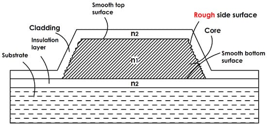
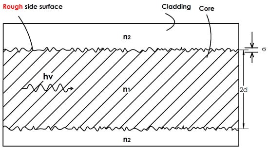
Figure 1 and Figure 2 illustrate the cross-sectional and top views of a conventional single-cladding rib waveguide, which is comprised of a waveguide core and a single layer of low-refractive-index cladding. The core has a rough side surface. In this case, the propagation loss coefficient, , in decibels per centimeter, caused by the scattering of the sidewall can be derived as [26,27]
where is the RMS scattering coefficient, is the wavenumber in vacuum, is the operational wavelength, is the refractive index of the core, is the refractive index of the cladding, is the effective refractive index of the guided core mode, and is the width between two sidewalls, as illustrated in Figure 2. The function is a dimensionless function, which is linked to the properties of the waveguide, as given by:
where the normalized expressions of coefficients and can be expressed as
where is the correlation length of the rough surface of the sidewall. Equations (1)–(4) show that the scattering-induced loss coefficient, heavily depends on the roughness of the sidewall surface, and the refractive index difference, between the core and cladding. The higher the roughness, the greater the loss is. The larger the difference between the core and cladding, the greater the propagation loss is.
Figure 1.
A sketch of a cross-sectional view of a conventional single cladding rib waveguide, consisting of a substrate, an insulating layer, a high-refractive-index core, and a low-refractive-index overlay. The sidewall surface of the high-refractive-index strip core is rough, causing scattering loss.
Figure 2.
A top-view sketch of a conventional single-clad waveguide, consisting of a substrate, an insulating layer, a high-refractive-index core with a refractive index n1, and a low-refractive-index overlay with a refractive index n2. The width of the waveguide is 2d. The sidewall surface of the high-refractive-index strip core is rough, having a roughness of .
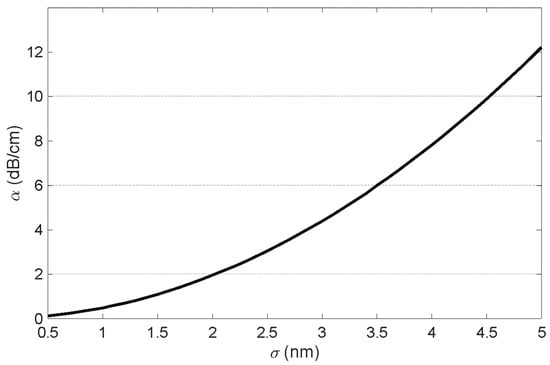
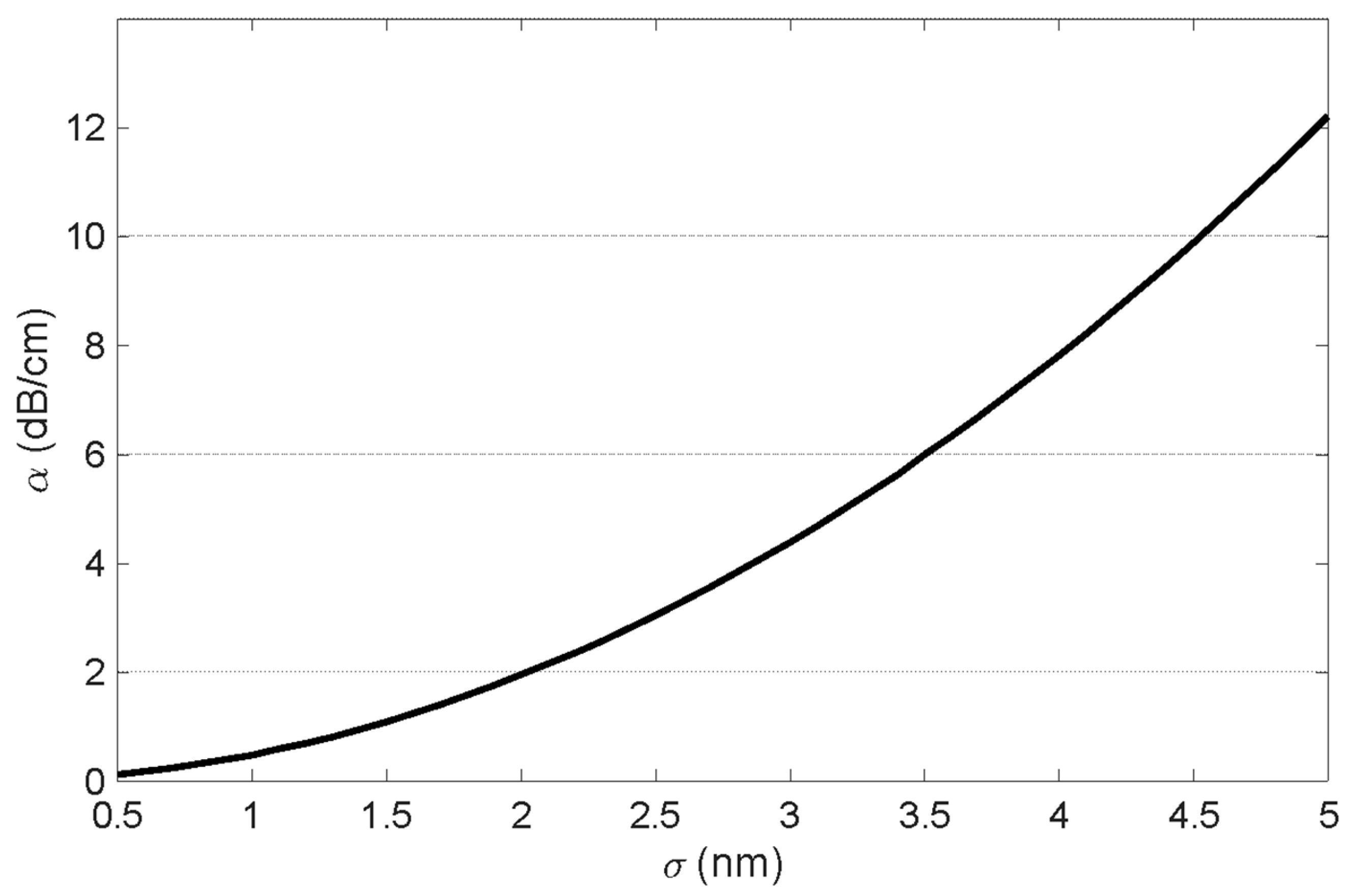
To gain a quantitative understanding of the relationship among the propagation loss coefficient, surface roughness, and the refractive index difference between the core and cladding, we computed the propagation loss using realistic parameters and a relatively accurate approximation. We assume that and . In Example 1, we compute the propagation loss of a typical lithium niobate rib waveguide for the case of an ordinary wave, including a lithium niobate core with a refractive index of, and silicon dioxide cladding with a refractive index of . Figure 3 shows the computed propagation loss coefficient, as a function of sidewall roughness, expressed in nanometers (nm). One can see that the propagation loss increases rapidly with increasing sidewall roughness. The propagation loss coefficient is as high as when (a typical value of an RIE-etched surface). However, the propagation loss coefficient decreases rapidly as the roughness decreases. The propagation loss coefficient is reduced to a very low level when .
Figure 3.
The computed propagation loss coefficient in dB/cm vs. the sidewall roughness in nm for the conventional step-index lithium niobate (LN) waveguide. The following parameters are used in computation: and . The loss is high at around 12.2 dB/cm, with a roughness of 5 nm.
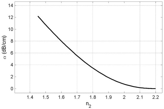
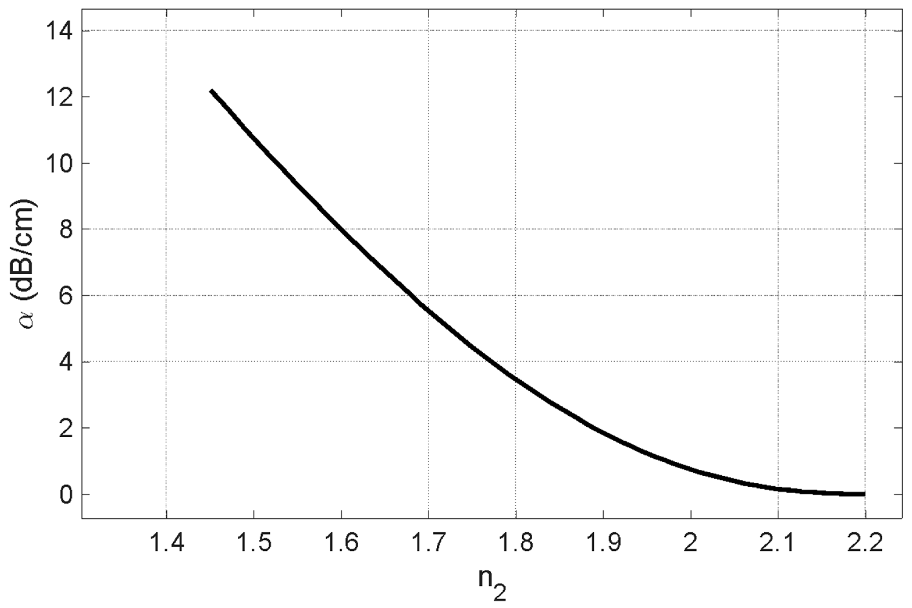
In addition to reducing the sidewall roughness to mitigate the scattering loss, another approach is to reduce the refractive index difference between the core and the cladding. As an example, we compute the propagation loss of a rib waveguide, including a lithium niobate core with a refractive index of and a cladding with different refractive indices. In the computation, we also assume that and . Figure 4 shows the computed propagation loss, as a function of the cladding refractive index. One can see that the propagation loss reduces as the refractive index difference between the core and cladding, decreases. When (corresponding to the case of ), the propagation loss coefficient, is dramatically reduced from 12.21 dB/cm to a very small value of <0.01 dB/cm. In this case, the scattering loss becomes negligible even with a 5 nm roughness. However, although the propagation loss can be reduced by decreasing the RI contrast between the core and cladding, it can also result in increased bending loss when the bending radius is fixed, as described in detail in the next section.
Figure 4.
The computed propagation loss coefficient in dB/cm vs. the refractive index difference between the core and cladding for the conventional step index LN waveguide. The following parameters are used in computation: . The values are within the range of 1.45–2.20. The scattering loss decreases as the refractive index difference between the core and cladding reduces.
2.2. Effects of RI Contrast on Bending Loss
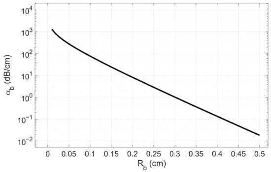
The bending loss of the optical waveguide depends heavily on the RI contrast between the core and cladding. For the step-index waveguide, the quantitative relationships among the bending loss coefficient, in dB/cm, bending radius, , in centimeters, and RI contrast between the core and cladding for the waveguide are similar to the case of optical fiber, which can be expressed by the following equations [28,29]
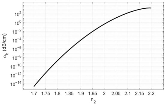
where a is the radius of the fiber, is the bending radius, and are the refractive indices of core and cladding, respectively, is the effective refractive index of a propagation mode, denotes the first-order modified Bessel function of the second kind, and is the wavenumber in vacuum. Based on Equations (5)–(7), one can see that the bending loss coefficient is very sensitive to the bending radius and the RI contrast between the core and cladding. Again, to gain a quantitative understanding of the relationships between the bending loss coefficient, bending radius, and the RI contrast between the core and cladding, we computed the bending loss coefficient using realistic parameters and a relatively good approximation. We assume that and . First, we computed the case of a titanium-doped LiNbO3 waveguide. In this case, we further assume that and . Figure 5 illustrates the computed bending loss coefficient as a function of bending radius. One can see that the bending loss coefficient is very sensitive to the bending radius. To achieve an acceptable level of bending loss coefficient (e.g., on the order of ), the required bending radius needs to be This severely limits the density of the PICs. Thus, a low RI contrast waveguide, such as a titanium-doped or proton-exchanged LiNbO3 waveguide, is not suitable for high-density PICs. To achieve a smaller bending radius while maintaining a low bending loss coefficient, it is necessary to increase the refractive index difference between the core and the cladding. Figure 6 illustrates the computed bending loss coefficients as a function of the refractive index difference at a very small bending radius. In the computation, we assume that , and values of are within the range of 1.72 to 2.20. One can see that the bending loss coefficient becomes negligibly small (on the order of when ). However, such an increase in RI contrast results in higher propagation scattering loss. Therefore, there is a fundamental trade-off between the propagation loss and bending loss.
Figure 5.
The computed bending loss coefficient, in dB/cm, vs. the bending radius, in cm. The following parameters are used in the computation: and . The bending loss coefficient increases rapidly as the bending radius decreases.
Figure 6.
The computed bending loss coefficient, in dB/cm, vs. the refractive index difference between the core and cladding. The following parameters are used in computation: and The bending loss coefficient increases rapidly as the refractive index contrast between the core and cladding decreases.
2.3. Self-Smoothed Gradient Refractive Index Cladding Waveguide to Achieve Both Low Propagation Loss and Low Bending Loss
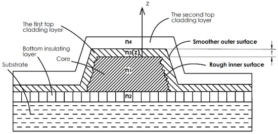
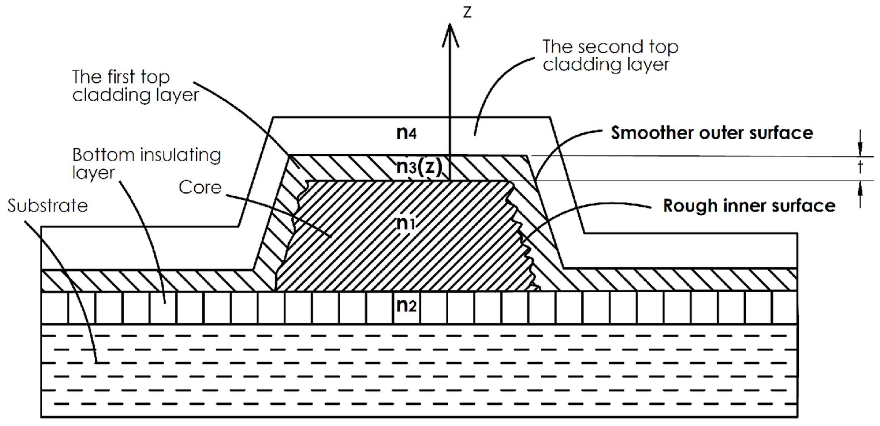
To solve the trade-off issue between the propagation loss and bending loss, we propose a novel self-smoothed double-cladding optical waveguide that can have both low propagation loss and low bending loss simultaneously, even with a rough sidewall () [30]. Figure 7 illustrates a cross-sectional view of our novel waveguide with an engineered self-smoothed, gradient-refractive cladding architecture. It is composed of (1) a substrate [e.g., made of silicon (Si), silicon carbide (SiC), aluminum nitride (AlN), Germanium (Ge), sapphire, diamond, etc.], (2) a low-refractive-index insulating bottom layer with a refractive index of n2 (e.g., made of SiO2, Al2O3), (3) a high-refractive-index waveguide core with a refractive index of n1 (e.g., made of LiNbO3, Si3N4, Si, Ta2O5, InP, GaAs, Ge, Al2O3, etc.), (4) a first gradient refractive index cladding layer and a side cladding layer n3(z), and (5) a second top and side cladding layer with a refractive index n4. The gradient index of the first cladding layer has the following properties: At the interface between the core and the first cladding layer, (i.e., z = 0), Then, gradually decreases as z increases. Finally, at the interface between the first cladding layer and the second cladding layer, where is the total thickness of the first gradient index cladding layer. To ensure a low propagation loss and a high mode confinement for low bending loss, the materials and shapes of the first and second cladding layers are precisely selected and engineered, which meet the following conditions: (1) The value of n3 is gradually changed as described above. (2) The refractive index of the second cladding layer, n4, is substantially lower than that of the fiber core, n1, ensuring a high mode confinement. (3) The roughness of the first cladding layer is also gradually reduced via a self-smoothing effect during the fabrication process of the first cladding layer [31,32], as illustrated in Figure 8, to be described in detail in Section 2.4. The combined self-smoothing effect of the first cladding layer and its gradient-index nature can greatly reduce the propagation loss coefficient by two orders of magnitude for the same sidewall roughness and the bending loss coefficient.
Figure 7.
The self-smoothed double-cladding waveguide architecture, which is composed of (1) a substrate, (2) a low-refractive-index insulating bottom layer with a refractive index of n2, (3) a high-refractive-index waveguide core with a refractive index of n1, (4) a top and side first cladding layer with a gradient refractive index of a thickness of “t”, and (5) a second top cladding with a refractive index of n4. The value of n4 is substantially lower than that of n1. Also, the outer surface of the first cladding layer is substantially smoother than that of the inner surface due to the self-smoothing effect of the fabrication process.
Figure 8.
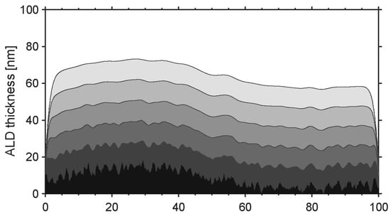
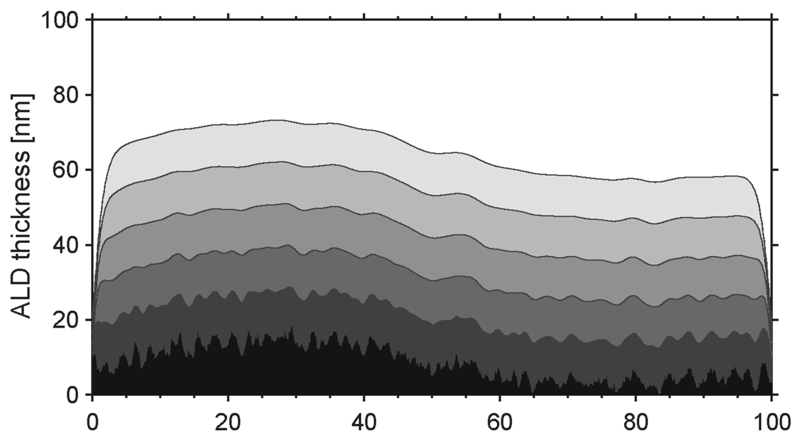
A sketch of the self-smoothing effect during the atomic layer deposition (ALD) process [31,32]. Both the surface roughness and the refractive index decrease during the ALD coating process.
2.3.1. A Theoretical Analysis of Propagation Loss
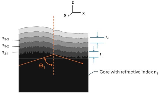
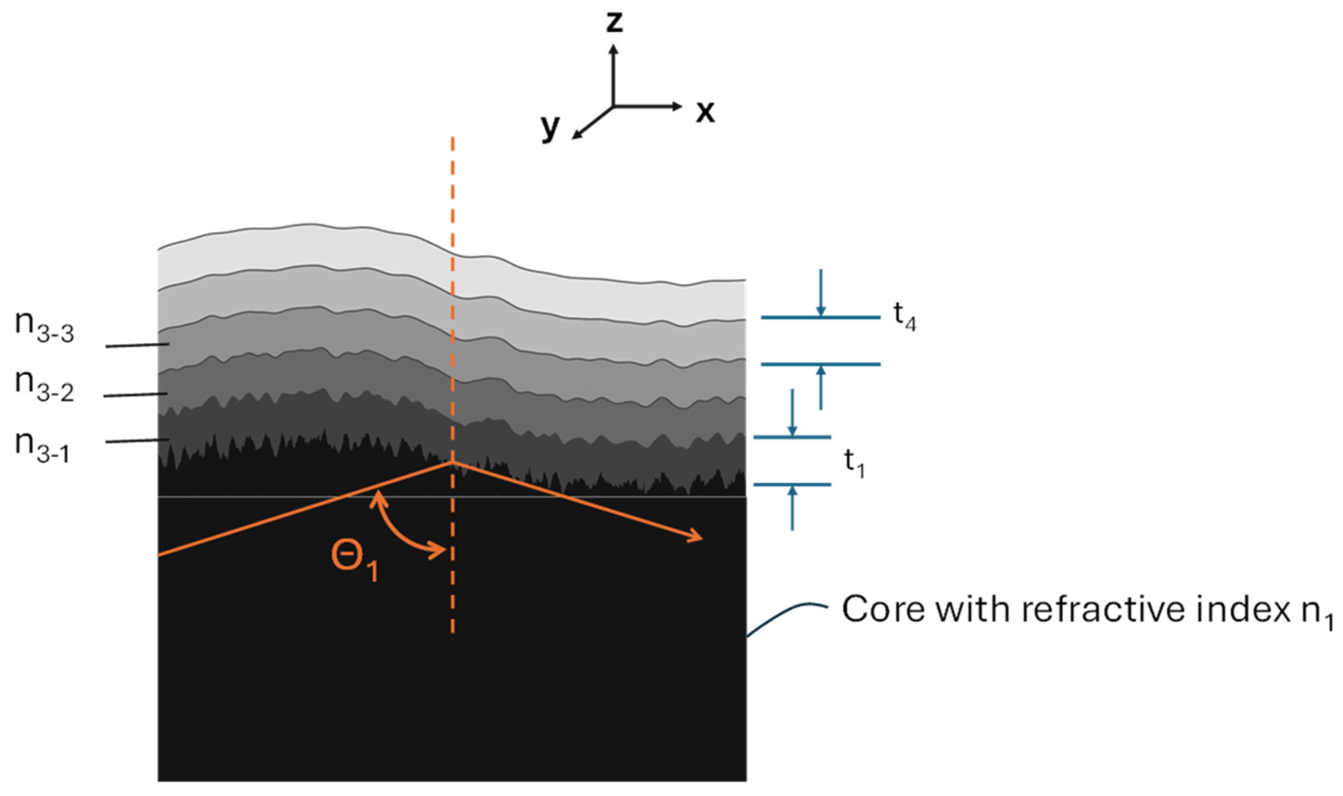
To conduct a quantitative analysis of the propagation loss of our self-smoothed gradient index cladding waveguide, we can assume that the gradient index first layer consists of multiple (N) sublayers, as illustrated in Figure 9. The refractive indices, thicknesses, and the roughness of the first sublayer, the second sublayer, the third sublayer, …, the Nth sublayer are n3-1, t1, ; n3-2, t2, ; n3-3, t3, …, and n3-N, tN, respectively. Due to the random nature of each scattering sublayer, we can ignore the interference among the scattered light from different sublayers. In this case, the total scattering loss, , can be derived as,
where and are the scattering coefficients caused by the boundary between the core and the first cladding, between the first cladding and the second cladding, between the second cladding and the third cladding, and between the (N-1) and N layers, respectively. The term denotes the percentage of leaked evanescent wave to the boundary between the first and second claddings. The term denotes the percentage of leaked evanescent wave to the boundary between the second and third claddings. The term denotes the leaked evanescent wave between the (N-1) sublayer and the N sublayer. is the angle of incidence at the boundary between the core and the first cladding.
Figure 9.
A sketch of the self-smoothed gradient index first cladding layer, consisting of multiple sublayers.
We further assume that the thicknesses of all the sublayers are the same (i.e., ) and that the refractive index difference between adjacent layers is also the same (i.e., ). For ease of expression, we also assume that In this case, Equation (8) can be approximately expressed as
where is the roughness between the (m − 1)th and mth layer; the normalized expressions of the coefficients x and can be expressed as
Based on Equations (8)–(13), the total scattering coefficient, can be quantitatively computed. The result confirms that the scattering loss can be reduced by two orders of magnitude, as described in detail in Section 3.
2.3.2. A Theoretical Analysis of Bending Loss for Gradient Index Cladding Waveguide
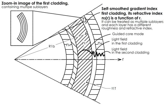
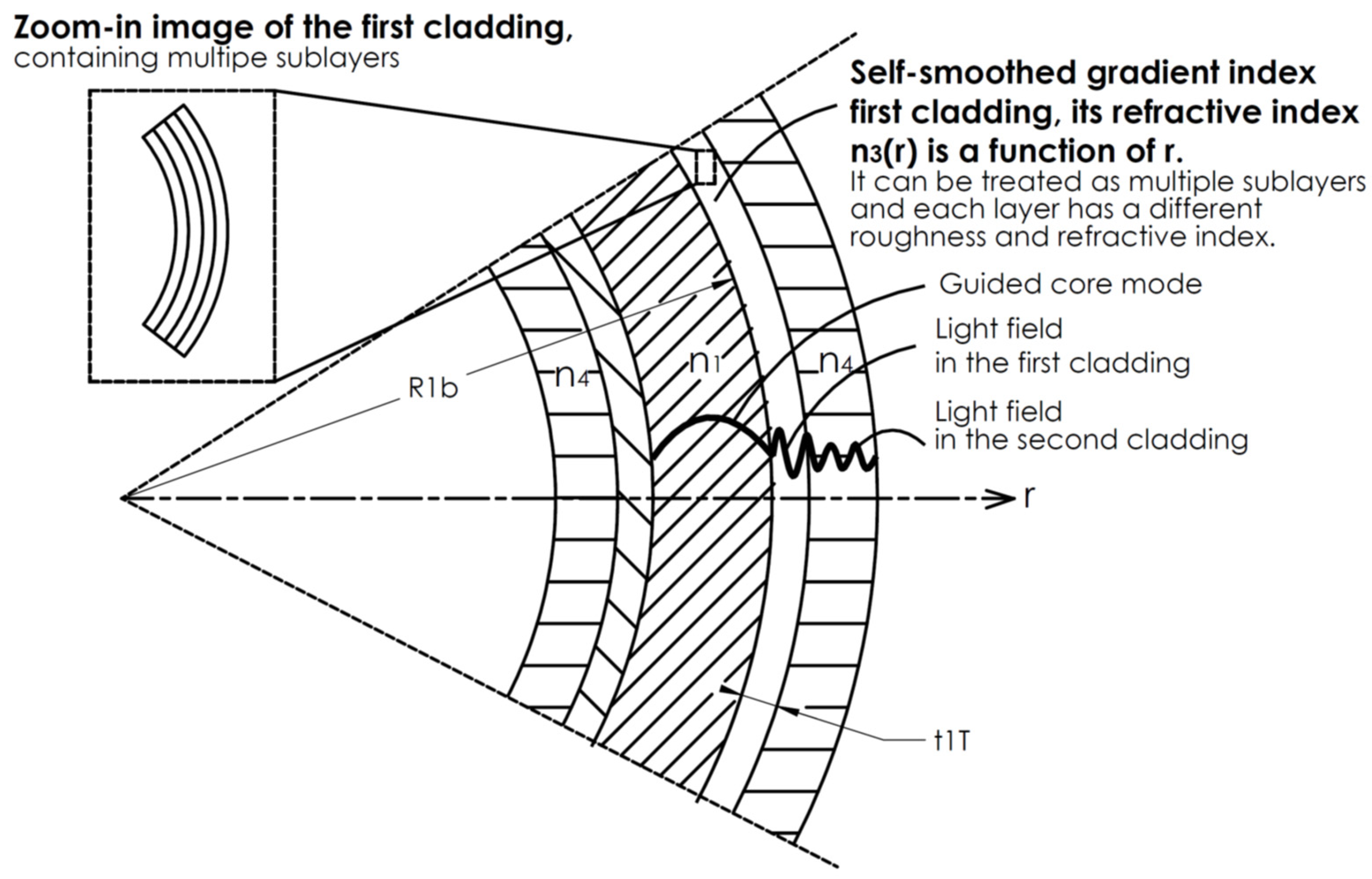
Figure 10 depicts a bent self-smoothed gradient index cladding waveguide, consisting of a bent core, a bent first cladding layer, and a bent second cladding layer. The refractive indices of the fiber core and the second cladding are n1 and n4, respectively. The first cladding layer is a gradient index layer, whose refractive index varies from n1 to n4.
Figure 10.
A sketch of a bent self-smoothed gradient index proposed in this paper, consisting of a bent core, a bent self-smoothed gradient index first cladding layer that can be divided into N-sublayers, and a bent second cladding layer. The bending radius for the core is R1b.
To conduct a quantitative analysis of the bending loss of our self-smoothed gradient index cladding waveguide, we compute the bending loss with the two following cases: (1) a step-index cladding structure and (2) a gradient index cladding structure. For comparison between the step index and gradient index cases, we use a slightly different method, as described in [33], to compute the bending loss. The bending loss of a step-index cladding, is given by [33]
where is the refractive index of the fiber core, is the wavenumber in vacuum, is the critical angle, is the angle of propagation, is the operational wavelength, is the refractive index of the second cladding, is the width between two sidewalls of the core, and is the bending radius. Similarly, the bending loss of a gradient index cladding, is given by [33]
where is the refractive index of the fiber core, is the wavenumber in vacuum, is the critical angle, is the angle of propagation, is the operational wavelength, is the refractive index of the second cladding, is the width between two sidewalls of the core, and is the bending radius.
Based on Equations (14) and (17), we quantitatively computed and compared the bending loss coefficient for our self-smoothed gradient index cladding waveguide and a typical step index cladding waveguide, as described in detail in Section 3. The result confirms that the bending can remain within the acceptable range by adding a self-smoothed gradient index cladding layer, consistent with a previous study on the bending of a gradient index fiber [33]. In summary, our unique self-smoothed gradient-index cladding can greatly (two orders of magnitude) reduce the propagation loss while having an acceptable bending loss. Thus, low-loss, high-density PICs can be realized.
2.4. Methods to Realize Self-Smoothed Double-Cladding Waveguide
Multiple methods can be employed to realize a self-smoothed double-cladding waveguide. The first method is to fabricate the top first cladding layer via atomic layer deposition (ALD), offering the following advantages: (1) the core is fully wrapped by the first cladding layer due to the conformal nature of ALD coating, (2) the sidewall roughness of the core is automatically smoothed because it is easier to deposit film in the valleys than on the peaks [31], (3) the gradient index can be fabricated by changing the cycle numbers of different materials, and (4) ALD can be a low temperature deposition process and compatible with other semiconductor chip fabrication processes. The detailed selection of materials for ALD coating depends on the waveguide core material.
For example, for the LiNbO3 waveguide core, we can use ALD-coated TiO2/SiO2 or TiO2/Al2O3 nanolaminates as the first gradient index cladding layer because it has a low optical loss and its refractive index can be adjusted to the required value by controlling the ratio of ALD cycles between TiO2 and SiO2 [34]. At the beginning of ALD coating, there are more ALD cycles of TiO2 than those of SiO2, resulting in a refractive index close to LiNbO3 (2.21). At the later stage of ALD coating, there are more ALD cycles of SiO2 than those of TiO2, resulting in a refractive index close to that of Al2O3 (1.65) or SiO2 (1.45). We can reasonably assume that this self-smoothed gradient index first cladding is divided into 100 sublayers, each with a thickness of 10 nm. The total thickness is The refractive index difference between adjacent sublayers is (2.21 – 1.45)/100 = 0.0076 if SiO2 is used as the second cladding layer. The second lower refractive index layer can also be fabricated using an ALD-conformally coated Al2O3 or SiO2 layer because their refractive indices ( and ) are much lower than those of the waveguide core. In addition to TiO2/SiO2 and TiO2/Al2O3, other nanolaminates, such as Ta2O5/Al2O3 can also be used.
Another example is a silicon nitride (Si3N4) waveguide core. Although the sidewall roughness of Si3N4 can be made smooth by using the photonic Damascene (additive) process, there are still a lot of challenges as summarized below: (1) it is difficult to have good dimension control due to the use of high-temperature (>1000 °C) thermal reflow; (2) it can have non-uniformity due to the need to polish out extra Si3N4 via a CMP process; and (3) it can generate metal impurities from processing that affect the transmission. On the other hand, ICP-RIE dry etching (subtractive) offers precise dimensional control and high thickness uniformity across the wafer, making it suitable for wafer-scale mass production. However, the sidewall roughness of the Si3N4 waveguide fabricated by dry etching is higher than that of the waveguide fabricated by the photonic Damascene process; this is because the latter does not benefit from the smoothing effect of the smooth sidewalls of the thermally reflowed trenches. To overcome this fundamental limitation, we can use our self-smooth gradient index Si3N4 waveguide. Since the refractive index of the Si3N4 waveguide core is around at a wavelength of 1550 nm, we can use ALD-conformally coated TiO2/SiO2, TiO2/Al2O3, HfO2/Al2O3 [35], or HfO2/SiO2 [36] as the first gradient index cladding layer. Again, the refractive index can be adjusted to the required profile by controlling the ratio of ALD cycles among TiO2/SiO2, TiO2/Al2O3, HfO2/Al2O3, and HfO2/SiO2. Again, the second lower refractive index layer can also be fabricated using an ALD-conformally coated Al2O3 or SiO2 layer because their refractive indices ( and ) are much lower than those of the waveguide core.
One more example is a silicon (Si) waveguide core. Since the refractive index of the Si waveguide core is around at the wavelength of 1550 nm, we can use ALD-coated amorphous silicon/silica (a-Si/SiO2) nanolaminates [37] as the first self-smoothed gradient index cladding layer because the required gradient refractive index profile can be achieved by controlling the ratio of ALD cycles between a-Si and SiO2.
In addition to ALD coating, other physical/chemical deposition methods, such as evaporation, sputtering, pulsed laser deposition, chemical vapor deposition, and metal–organic chemical vapor deposition (MOCVD), can also be employed to fabricate the first and second cladding layers. To ensure conformal coating, targets may need to be properly moved. Furthermore, dip-coated polymer and/or glass can be used to fabricate the first and second claddings if their refractive indices meet the requirements. For example, high-refractive-index polymers can have a refractive index within a range of 1.7 to 1.9 [38], which can serve as the first gradient index cladding layer for Si3N4, or sapphire waveguide cores, due to the following reasons: First, their refractive indices can be close enough to the waveguide core. Second, the refractive index can be adjusted by controlling the material composition to achieve the required gradient index profile. Third, the dip coating method exhibits good self-smoothing. Fourth, the dip coating process is quick and cost-effective.
Note that although gradient-index cladding has been mentioned in a prior patent [39], it does not disclose the self-smoothed gradient-index cladding. It also does not teach how to effectively realize the self-smoothed gradient-index cladding.
3. Results
3.1. Quantitative Computational Study on Propagation Loss and Bending Loss of Self-Smoothed Gradient Index Cladding Waveguide
To ensure that the proposed self-smoothed gradient-index double-cladding waveguide breaks the trade-off between propagation loss and bending loss, achieving both low propagation loss and bending loss even with noticeable sidewall roughness (e.g., ), we conducted the following quantitative computational study.
3.1.1. A Quantitative Computational Study on Propagation Loss
We first conducted a quantitative theoretical analysis of the propagation loss due to the sidewall-roughness-induced scattering in the self-smoothed gradient index waveguide. To gain a quantitative understanding of the reduction in scattering loss enabled by the self-smoothed gradient index cladding structure, we computed the propagation loss using realistic parameters and a relatively accurate approximation. We assume that and . We further assume that the self-smoothed gradient index of the first cladding layer, is divided into 100 sublayers, and the thickness of each sublayer is The refractive index of each sublayer is gradually reduced. The refractive index difference between the adjacent sublayers is, . The effective refractive index of the mth sublayer is . The scattering coefficient is also gradually reduced due to the self-smoothing effect of the conformal coating process. Based on the experimental data of previous studies on the smoothing effect of ALD coating [31,32], we derived the following empirical formula for the roughness of each sublayer, as given by
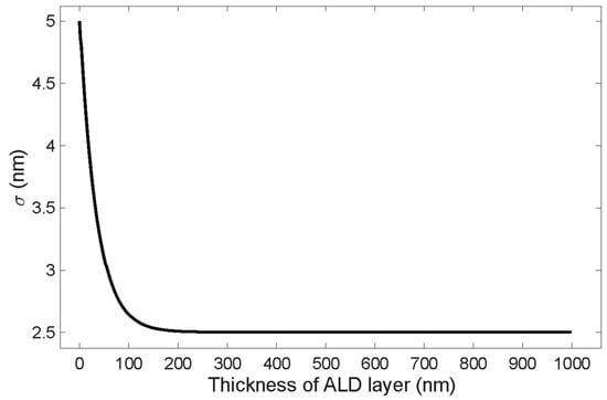
where is the surface roughness of the waveguide core, and x is the location of the sublayer in nm, as illustrated in Figure 10. We can see that the roughness decreases rapidly and then reaches a plateau. The plateau value depends on the initial roughness of the fiber core [31,32]. A conservative value of is used in our computation. As an example, Figure 11 illustrates the computed as a function of x in nm when The shape of the curve matches the previously reported experimental curve [31,32].
Figure 11.
The computed as a function of x in nm when Surface roughness decreases during the ALD coating process.
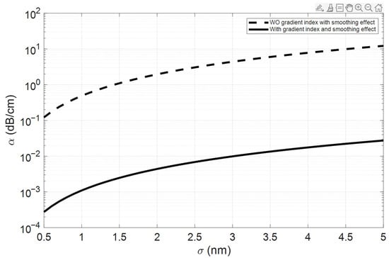
Based on Equations (14) and (17) and the above realistic parameters, we quantitatively computed the propagation loss coefficient due to the sidewall-roughness-induced scattering. The solid line in Figure 12 shows the computed propagation loss for our self-smoothed gradient index cladding layer. For comparison, we also computed the propagation loss without our gradient index cladding layer, as indicated by the dashed line in Figure 12. We can see that the propagation loss decreases as decreases in both cases. However, the propagation loss coefficient for our self-smoothed gradient index first cladding layer is dramatically lower (by two orders of magnitude) than that for the case without it. The propagation loss coefficient is still very low , even when Such a dramatic reduction in the propagation loss is because the scattering-induced loss of each sublayer is almost proportional to the in which two terms are from and “0.5” from the term Furthermore, the propagation loss coefficient is proportional to the square of Thus, a very low propagation loss coefficient on the order of 0.02dB/cm can be achieved even with a rough sidewall (), representing a technological breakthrough in photonic integrated circuits.
Figure 12.
The computed propagation loss coefficient due to sidewall-roughness-induced scattering for the cases with (solid line) and without (dashed line) our self-smoothed gradient index first cladding layer, under the following parameters: and . The first gradient index cladding layer is composed of 100 sublayers, and each sublayer has a thickness of The refractive index of each sublayer is gradually reduced, and the refractive index difference between adjacent sublayers is . The propagation loss coefficient is reduced by more than two orders of magnitude with our self-smoothed gradient index cladding.
3.1.2. A Quantitative Computational Study on Bending Loss
We also conducted a quantitative theoretical analysis of the bending loss of our self-smoothed gradient index cladding waveguide. To obtain a quantitative understanding of the bending loss, we computed it using Equations (14) and (17) with the following realistic parameters and a relatively accurate approximation. We assume that and . Figure 13 shows the computed bending loss coefficient, αs, in dB/cm, vs. the bending radius, in for the case without our self-smoothed gradient index cladding layer. We can see that the bending loss coefficient is very small (), even for a small bending radius due to the large refractive index contrast. Furthermore, we computed the bending loss coefficient for the case of our self-smoothed gradient index cladding layer, as illustrated in Figure 14. We can see that the bending loss is still within the acceptable range (<1 dB/m = 0.01 dB/cm) at a small 20 micron bending radius.
Figure 13.
The computed bending loss coefficient without the self-smoothed gradient index first cladding layer, under the following parameters: and .
Figure 14.
The computed bending loss coefficient for the cases with our self-smoothed gradient index first cladding layer, under the following parameters: and . The bending loss coefficient remains at the acceptable, low loss level of <0.01 dB/cm, even at a small bending radius.
3.2. Quantitative Analyses on the Mode Field Profile and Confinement
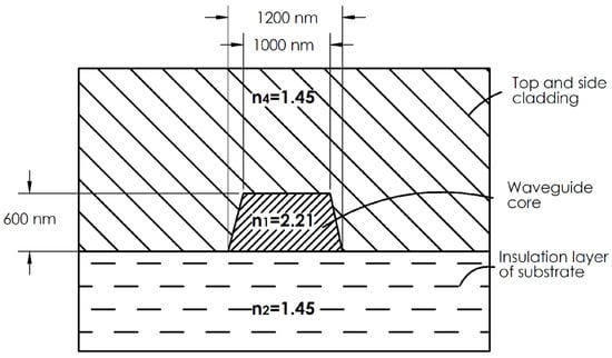
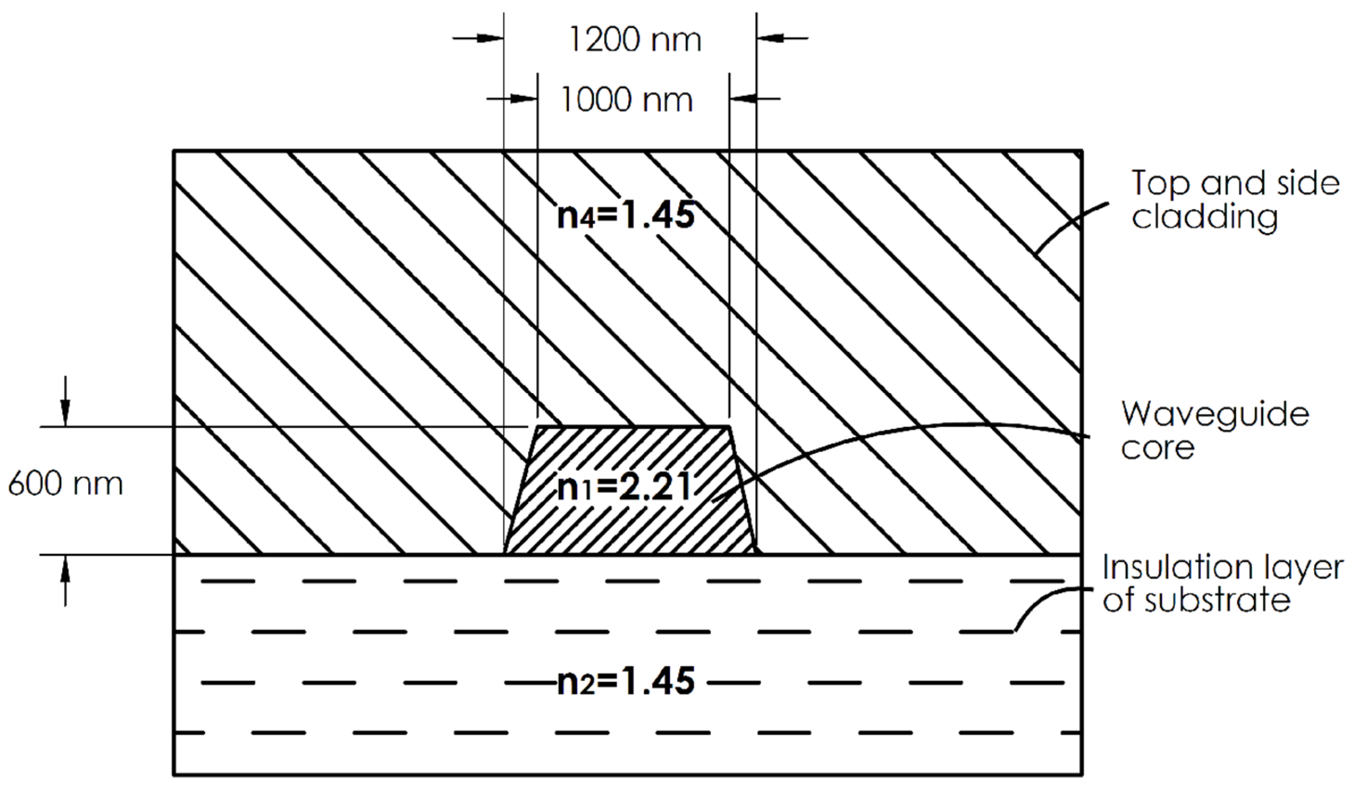
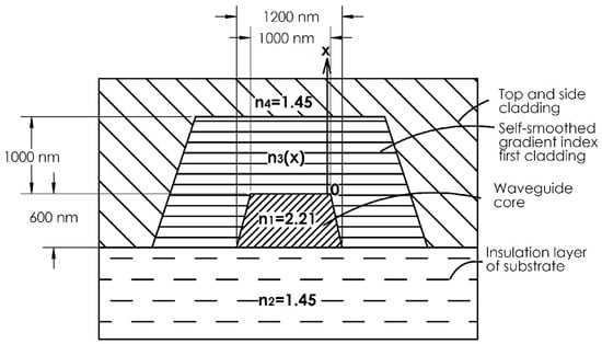
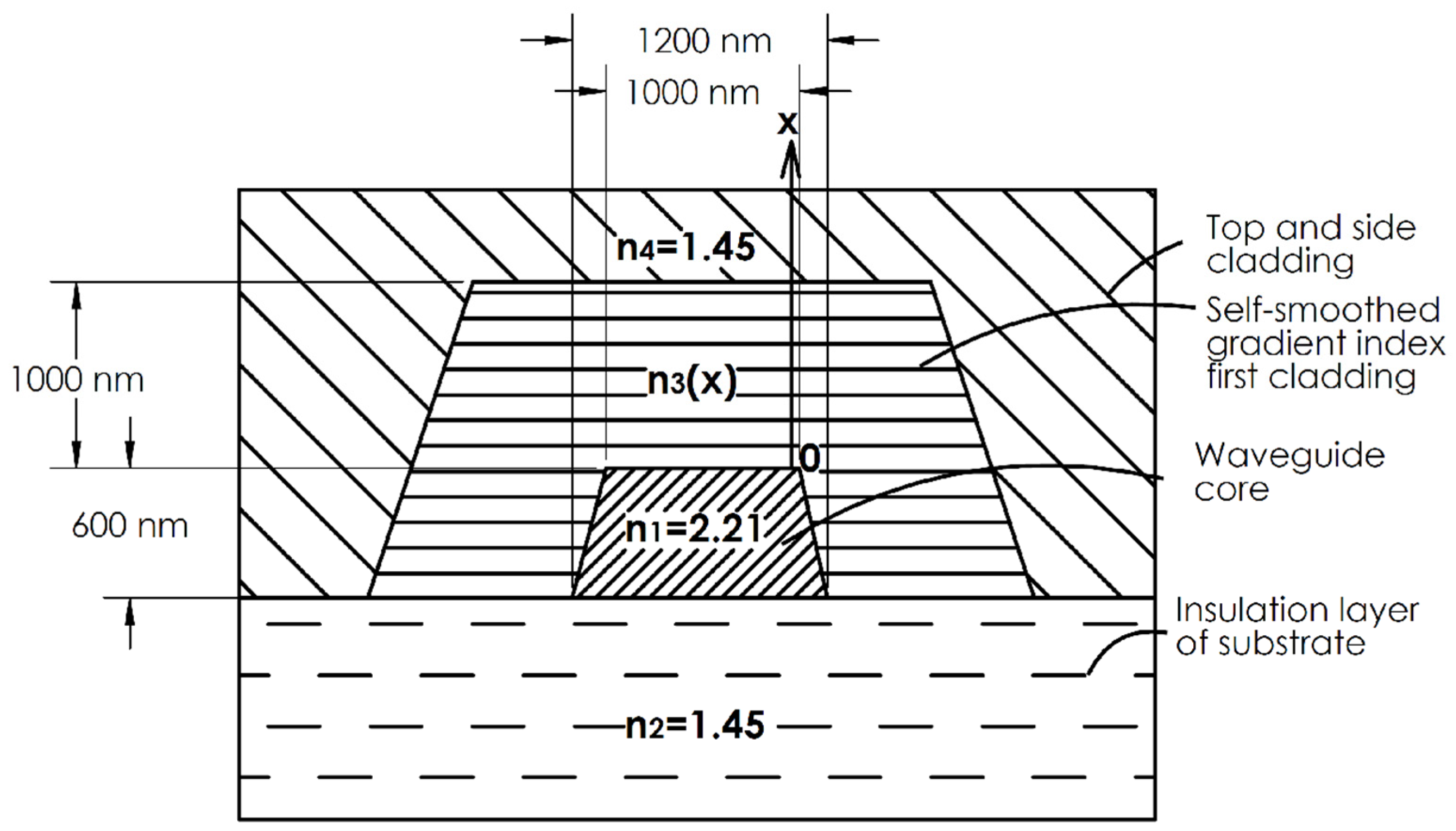
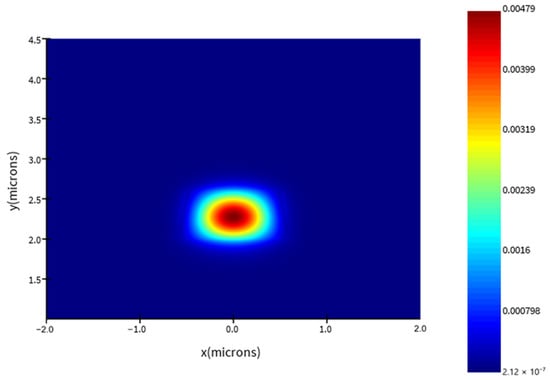
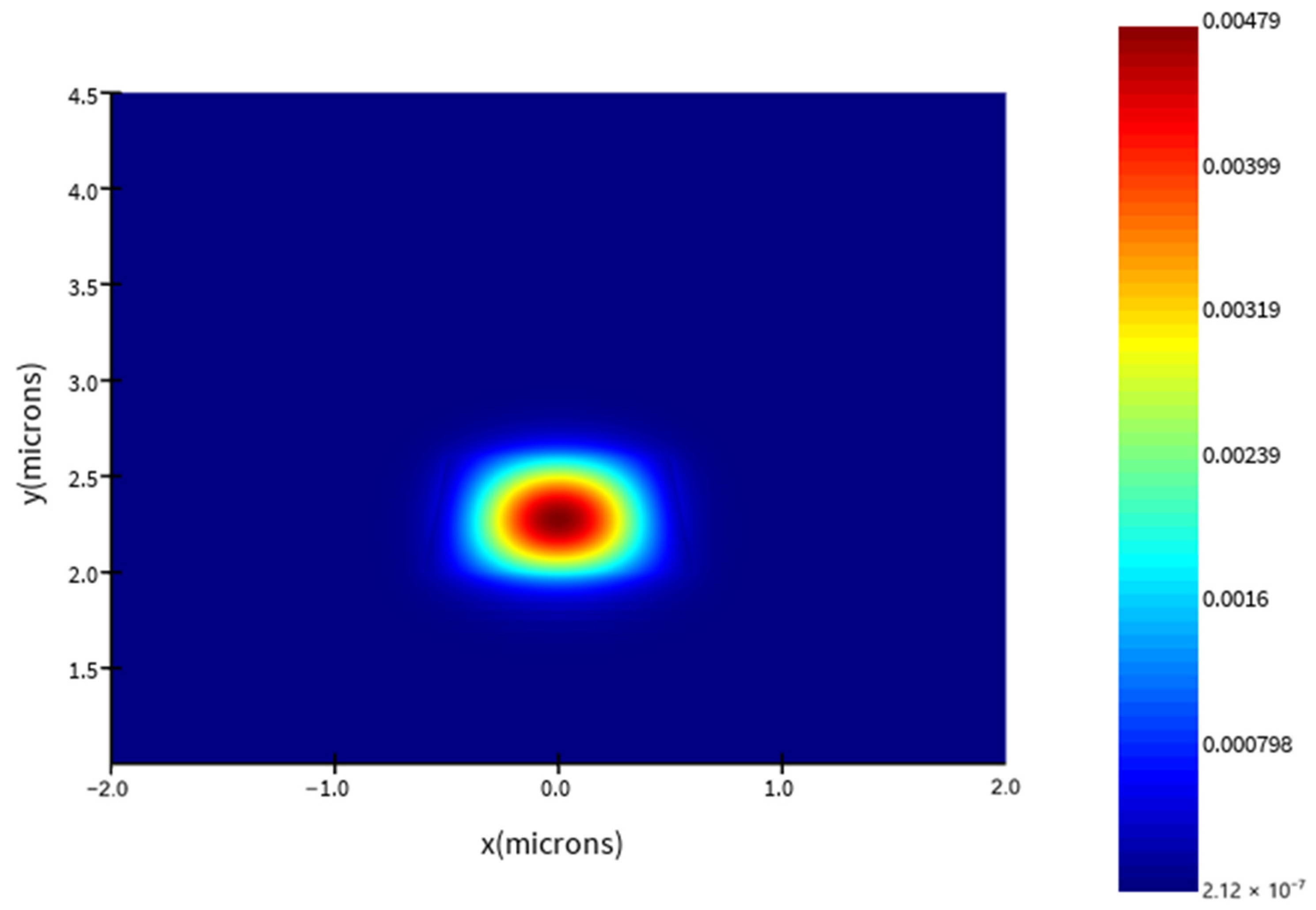
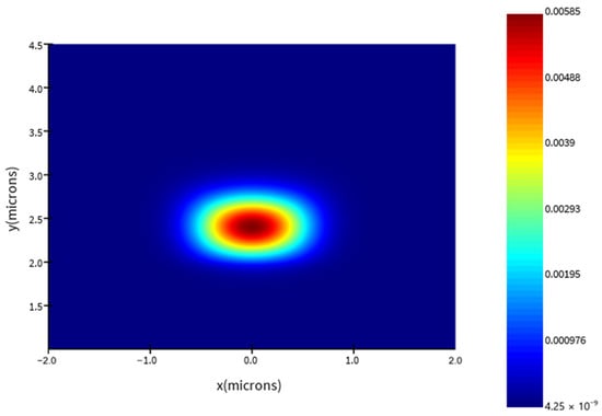
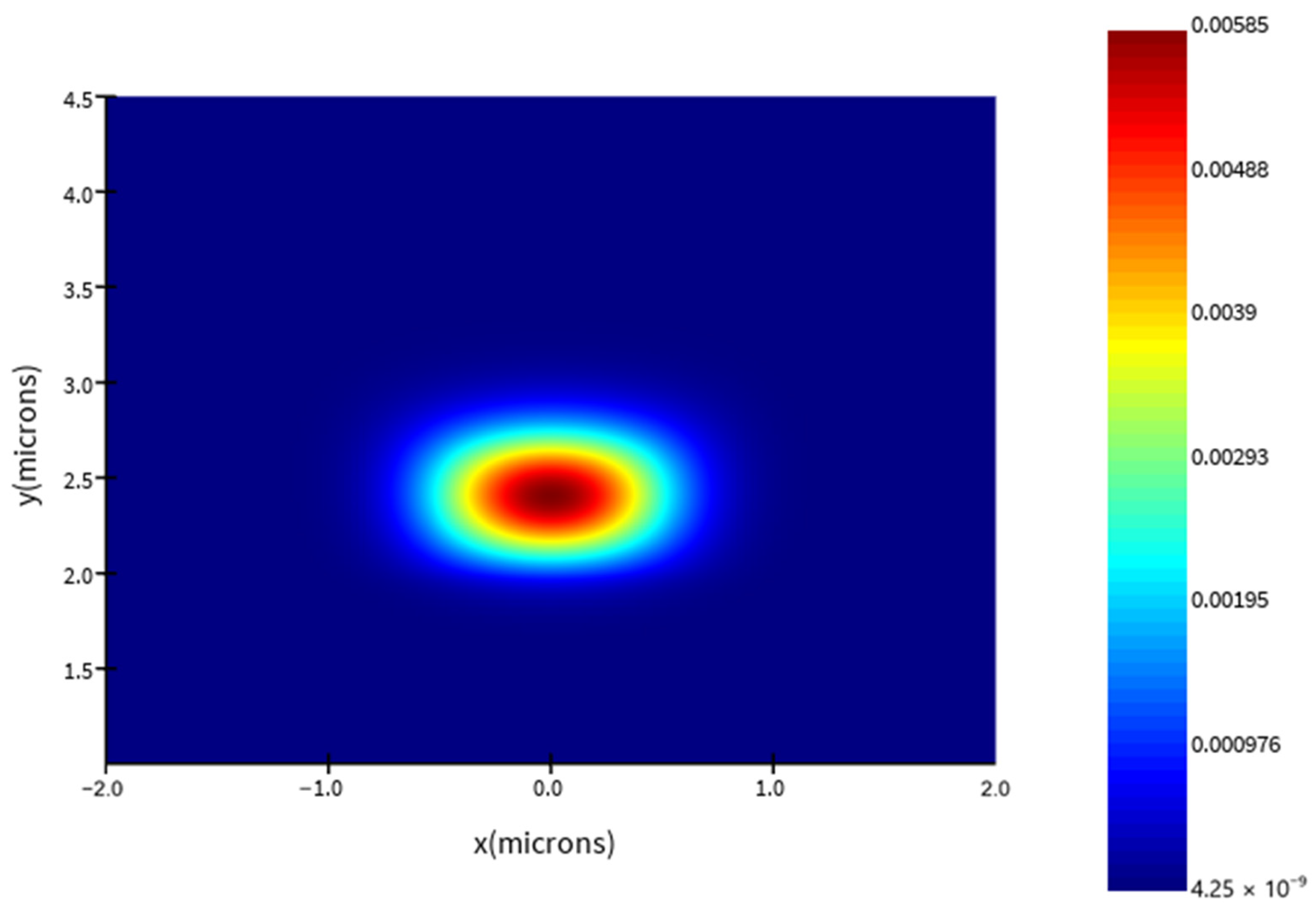
We also conducted quantitative analyses on the mode field profile and confinement. The Ansys Lumerical FDTD software (version 2025.R1.1.2, Ansys, Inc., Canonsburg, PA, USA) is used to compute the mode file profile. Figure 15 shows a cross-sectional view of a conventional rib-shaped waveguide for computation, including the geometric dimensions and the refractive indices of the waveguide core, n1 = 2.21, the substrate insulation layer, n2 = 1.45, and the top and side claddings, n4 = 1.45, respectively. The widths of the top and bottom and the height of the waveguide core are 1000 nm, 1200 nm, and 600 nm, respectively. Figure 16 shows a cross-sectional view of our self-smoothed gradient index cladding rib-shaped waveguide for computation. A first self-smoothed gradient index cladding layer is added, which has a total thickness of 1000 nm. The refractive index of the first cladding layer, is gradually reduced from the core to the second cladding. For example, n3(0) = 2.21, n3(500) = 1.83, and n3(1000) = 1.45, respectively.
Figure 15.
A cross-sectional view of a conventional rib-shaped waveguide, with a height of 600 nm, a top width of 1000 nm, and a bottom width of 1200 nm. The core has a high refractive index of and the cladding has a low refractive index of .
Figure 16.
A cross-sectional view of our self-smoothed gradient index cladding rib-shaped waveguide. The core size is the same as the case of conventional single-step index cladding, as illustrated in Figure 15. However, it has two claddings. The first cladding is a self-smoothed gradient index cladding. Its refractive index is gradually decreased from 2.21 to 1.45. The second cladding is a low-refractive-index cladding with a refractive index of .
In the computation, a 10 nm mesh size is used. Figure 17 shows the computed mode field profile for the conventional rib waveguide based on the data shown in Figure 15. Figure 18 shows the computed mode field profile for our self-smoothed rib waveguide based on the data shown in Figure 16. We can see that the two mode field profiles are very close. Thus, our novel self-smoothed gradient index cladding waveguide can dramatically (two orders of magnitude) reduce the sidewall-roughness-induced scattering loss while maintaining the same mode profile and confinement.
Figure 17.
A cross-sectional view of the computed mode field profile of a conventional rib-shaped waveguide.
Figure 18.
A cross-sectional view of the computed mode field profile of our self-smoothed gradient index cladding rib-shaped waveguide. One can see that the mode field profile is very similar to the case of a conventional single-step index cladding.
3.3. Experimental Investigation of Self-Smoothed Gradient Index Cladding
To demonstrate that the self-smoothed gradient index cladding can be fabricated, we also conducted a proof-of-concept experiment by growing self-smoothed gradient index cladding via atomic layer deposition (ALD)-grown non-uniformly cycled nanolaminates. For example, the refractive index of the LiNbO3 (LN) waveguide core is around 2.21 (nLN ≈ 2.21). We selected ALD-conformally coated, non-uniformly cycled Ta2O5/Al2O3 nanolaminates as the self-smoothed gradient index cladding because the refractive indices of ALD-coated tantalum pentoxide (Ta2O5) and alumina (Al2O3) are and respectively. Since the thickness of each ALD-coated sublayer is on the order of 1–100 nm, which is much smaller than the operating wavelength (e.g., ~ 1 µm), the effective refractive index of the composite cladding layer, can be estimated by using the following simple formula,
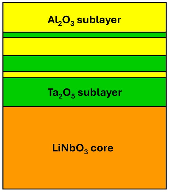
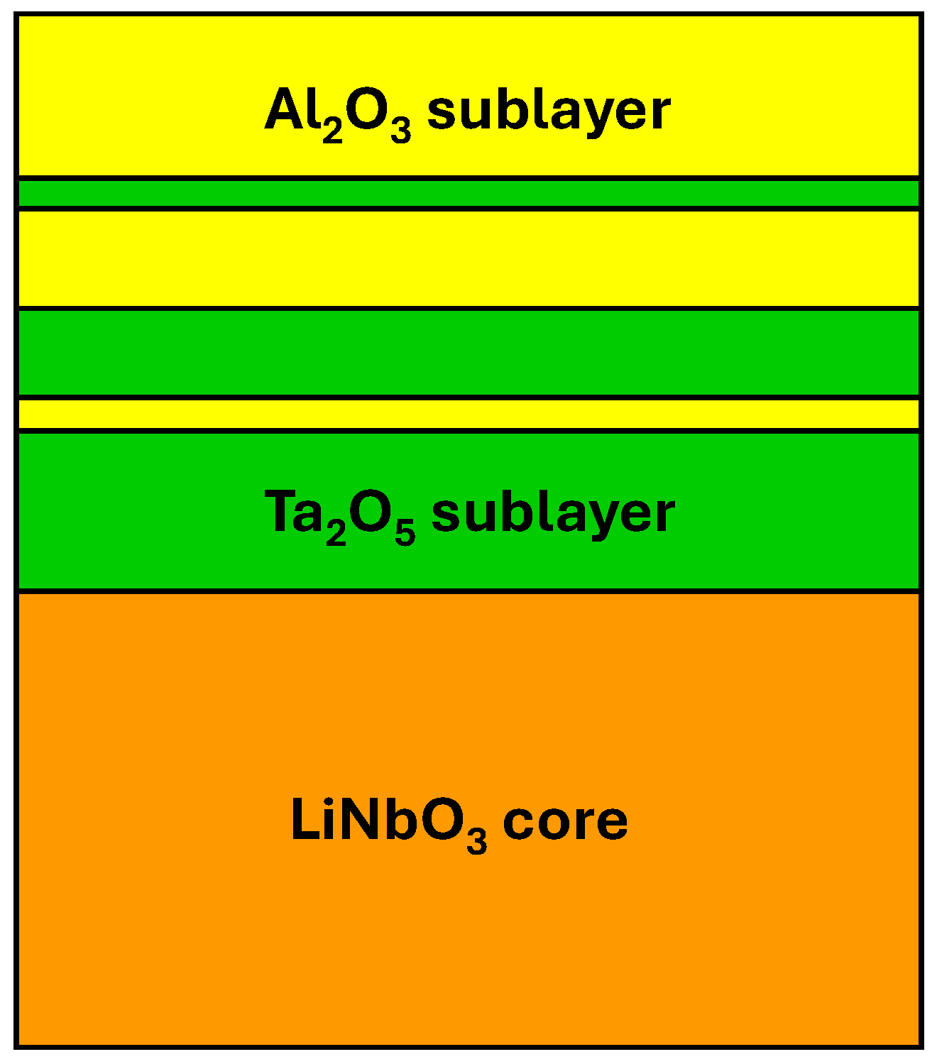
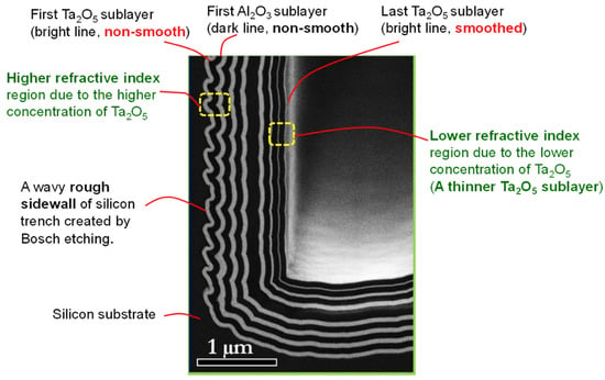
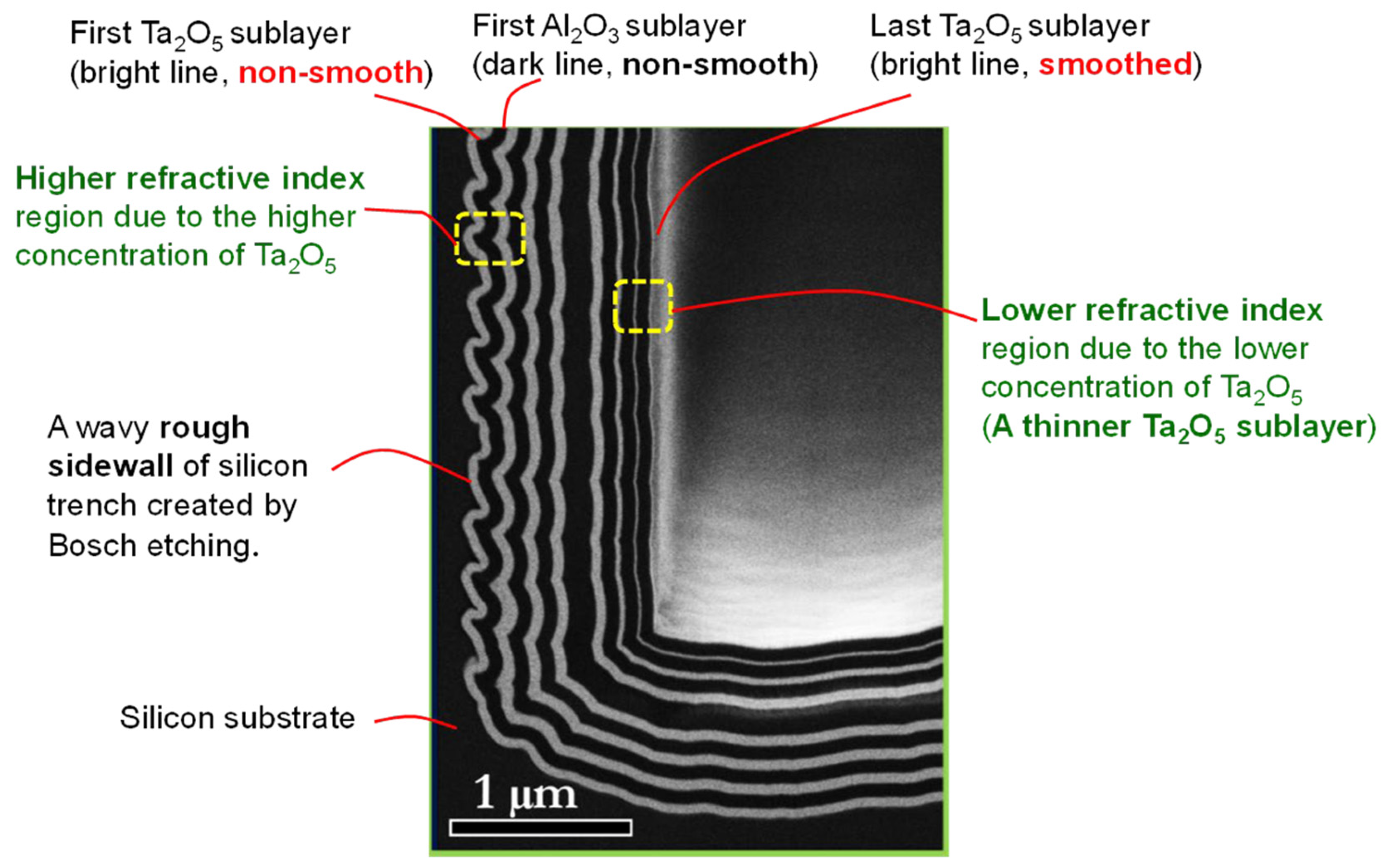
where represents the at.% of Ta2O5. As illustrated in Figure 19, at the beginning of ALD coating, there are more ALD cycles of Ta2O5 than those of Al2O3, resulting in a refractive index of around 2.20, close to LiNbO3 (2.21). At the later stage of ALD coating, there are more ALD cycles of Al2O3 than those of Ta2O5, resulting in a refractive index of around 1.65. This large refractive index contrast, Δn = 2.21 − 1.65 = 0.56, ensures strong light mode confinement and low bending loss in the waveguide. To verify this, we conducted the proof-of-concept experiment. Figure 20 shows the experimental result. The Ta2O5/Al2O3 nanolaminates were conformally coated on a silicon trench with a rough sidewall. The RMS roughness of the sidewall is around 100 nm. The RMS roughness after multiple ALD coating cycles is greatly reduced to <10 nm. Furthermore, the refractive index also gradually decreased due to the reduced Ta2O5 thickness. This experimental result confirms that we can realize self-smoothed gradient index cladding by using non-uniformly cycled Ta2O5/Al2O3 nanolaminates.
Figure 19.
An illustration of gradient index cladding by ALD-coated non-uniformly cycled Ta2O5/Al2O3 nanolaminates on a LiNbO3 substrate.
Figure 20.
A cross-sectional SEM image of ALD-deposited non-uniformly cycled Ta2O5/Al2O3 nanolaminates on the rough sidewall of a silicon trench. One can see that the smoothness increases during the ALD coating process. Also, at the beginning of the coating process, the high-refractive-index Ta2O5 layer is thicker, resulting in an overall high refractive index. At a later stage of the coating, the high-refractive-index Ta2O5 layer becomes thinner, resulting in an overall lower refractive index. Thus, a gradient index cladding can be achieved. This experimentally confirms that the self-smoothed gradient index cladding can be realized by ALD coating.
3.4. Experimental Investigation of Reducing the Roughness by Single-Layer Polymer Coating
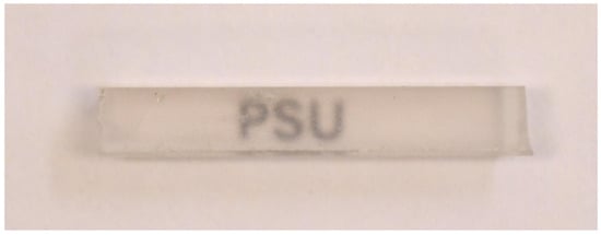
We also investigated the smoothing effect for dip-coated high-refractive-index polymer. A sapphire bar with a cross-section of 5 mm × 5 mm was used. The outer surface of the sapphire bar is rough, making it translucent, as shown in Figure 21. We cannot see clearly through the sapphire bar.
Figure 21.
A top view of the sapphire bar with rough outer surfaces.
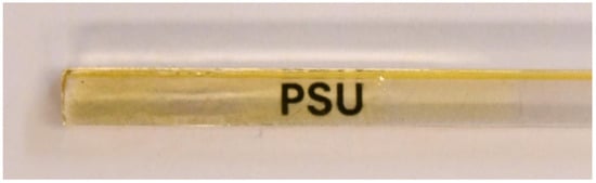
Then, we dip-coated the sapphire bar with a high-refractive-index polymer (). The translucent sapphire bar becomes transparent, as shown in Figure 22. We can now see through the dip-coated sapphire bar. The letter “PSU” under the sapphire bar is clearly shown in the image.
Figure 22.
A top view of a sapphire bar after dip coating in a high-refractive-index polymer. The translucent sapphire bar becomes transparent.
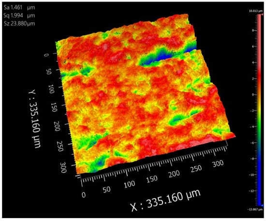
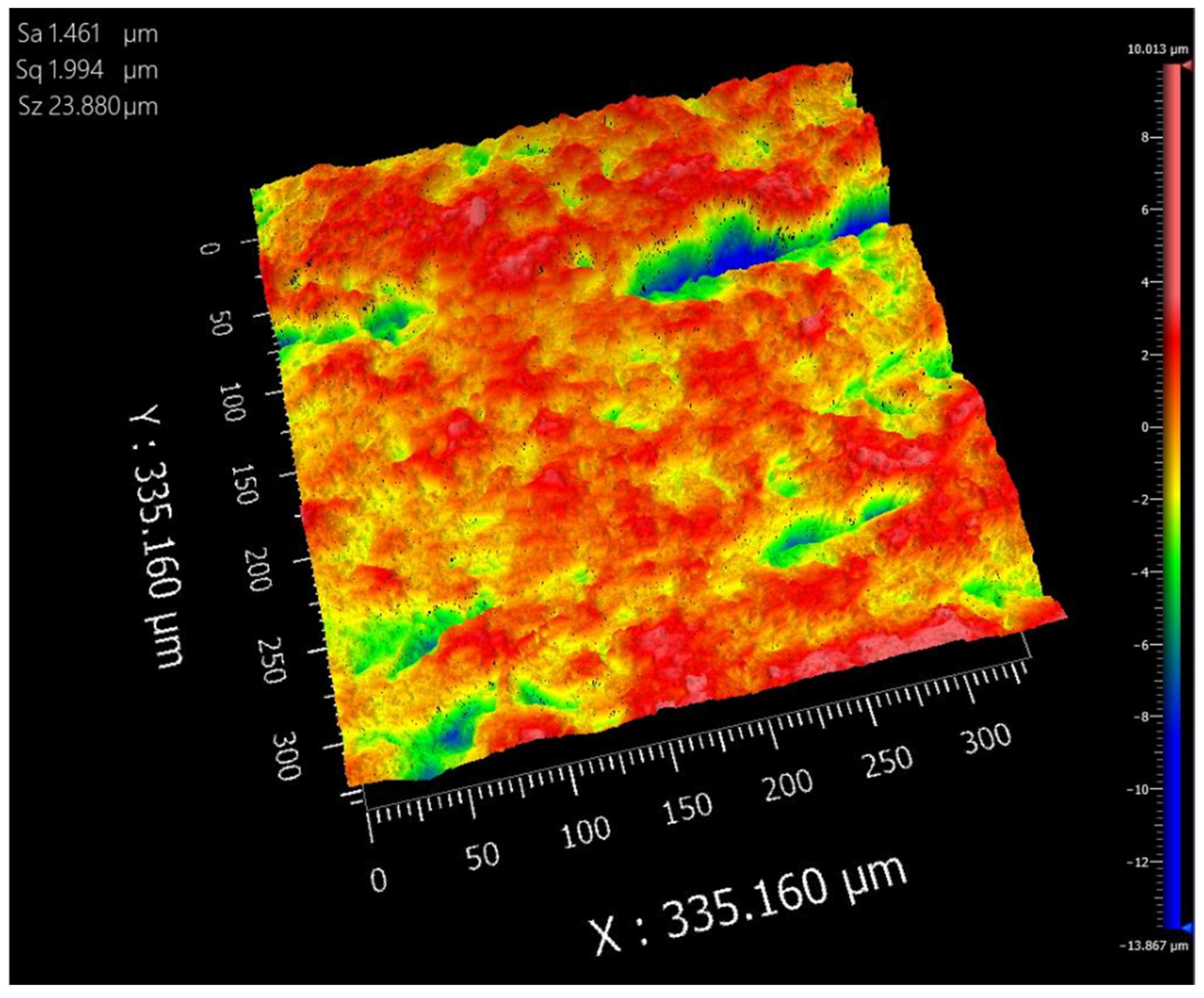
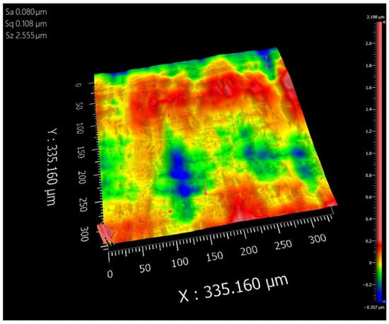
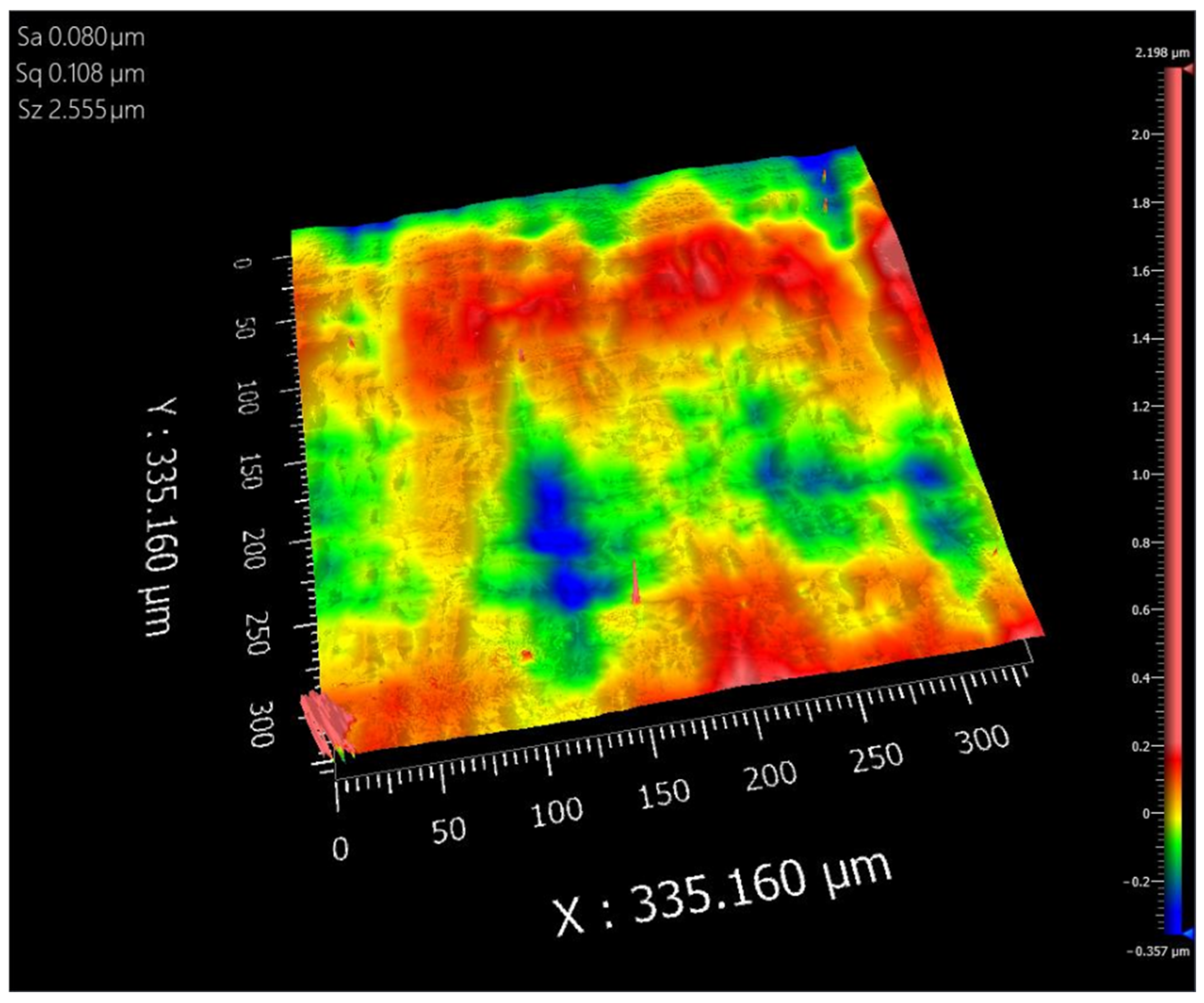
We also measured surface roughness using a Zygo Nexview 3D Optical Surface Profiler (Nexview, Zygo Corporation, Middlefield, CT, USA) with white light interferometry. Figure 23 and Figure 24 show the measured surface roughness before and after the polymer coating. We can see that the surface roughness has decreased significantly from ~2000 nm to ~100 nm.
Figure 23.
The surface roughness map before the polymer coating.
Figure 24.
The surface roughness map after the polymer coating. The surface roughness is greatly reduced from ~2000 nm to ~100 nm.
4. Discussion
4.1. A Comparison with Existing State-of-the-Art Propagation and Bending Loss Techniques in Different Platforms
To illustrate the usefulness of the proposed self-smoothed gradient index cladding method in reducing propagation and bending losses, we compared it with state-of-the-art methods across different platforms, as tabulated in Table 1. One can clearly see the advantages over the existing methods, as described below:
Table 1.
A comparison table between our proposed method and the existing state-of-the-art propagation/bending loss reduction techniques in different platforms.
For silicon nitride (Si3N4) waveguides, low loss (~0.01 dB/cm) has been achieved using very thin waveguides (<100 nm) or a high-temperature Damascene reflow process. However, these existing methods suffer limitations. For example, in a very thin waveguide, the dimensions of the optical mode are markedly different from those of a standard single-mode optical fiber (e.g., SMF-28) [23], resulting in high insertion and reflection losses when coupled directly. Specialized efforts such as edge coupling [40] and subwavelength grating couplers [41] are needed, thereby increasing the complexity and cost of photonic integrated circuits (PICs). On the other hand, the propagation loss can be much higher for thicker (>100 nm) Si3N4 waveguides without using a high-temperature Damascene reflow process. For example, for a 220 nm thick Si3N4 waveguide, the experimentally measured propagation loss is 0.5 dB/cm [15], and the sidewall roughness is around 1.1 nm, which is consistent with our theoretical result (0.48/cm) at a roughness of 1.1 nm without using our self-smoothed gradient index cladding technology. Furthermore, the high-temperature Damascene reflow process has drawbacks, including poor dimensional control and impurity-induced absorption losses. The major advantage of our proposed method is that we can achieve the same low propagation loss of 0.01 dB/cm without using thin waveguides or a high-temperature Damascene reflow process.
For lithium niobate (LN) waveguides, sidewall roughness remains a major issue. For the large refractive-index-contrast lithium niobate ridge waveguide, the propagation loss coefficient is generally high (>1 dB/cm). Even with gas-clustered ion beam smoothing, the sidewall roughness remains on the order of 8 nm [12]. For the single-mode waveguide (with a width around 1 micron), the TE/TM mode propagation losses are around 4 dB/cm and 8 dB/cm, respectively [12]. Even for the multimode case (with a width of 5 micron), the loss is still around 0.3 dB/cm [12]. Although a lower loss (~0.02 dB) can be achieved for titanium (Ti)-diffused or proton-exchanged LN waveguides, they exhibit large bending loss at small bending radii (e.g., 50 microns or smaller) due to the small refractive index contrast (on the order of 10−3). The major advantage of our proposed method is that we can achieve a low propagation loss of 0.01 dB/cm in a high-refractive-index-contrast LN ridge waveguide, resulting in both low propagation and bending losses at small bending radii.
For silicon-on-insulator (SOI) strip waveguides (with typical dimensions of 220 nm × 500 nm), propagation losses are primarily limited by sidewall-roughness-induced scattering [43,44,45]. The lowest recently reported propagation loss coefficient is around 0.28 dB/cm [43]. By using our proposed method, we can further reduce this propagation loss from the current 0.28 dB/cm to 0.01 dB/cm.
4.2. A Discussion of Self-Smoothing Effect for Different Coating Materials
The self-smoothing effect occurs during the ALD coating process at the micro- and nanoscale. We have observed this self-smoothing effect for many common ALD-coated amorphous materials, including Ta2O5, Al2O3, SiO2, and HfO2. This is because the ALD growth process is strictly conformal and self-limiting. On a rough surface containing micro- and nanoscale valleys, the walls of a valley grow inward toward each other from opposite sides. As the film thickens, the valleys narrow. Finally, the valley walls touch and merge (the so-called “valley pinch-off effect”), and the surface becomes smoother. The required thickness of the ALD-grown layer needs to exceed the root-mean-square (RMS) roughness. The exact amount of the smoothing depends on the initial material roughness, the thickness of the ALD-coated layer, and the ALD coating materials. It is possible to significantly improve the roughness from a value on the order of 100 nm to a much smaller value on the order of 1 nm, as shown in Figure 20. However, if the initial roughness is not that high (e.g., several nm), the amount of improvement may not be this high (from 100 nm to 1 nm, two orders of magnitude). But it is still possible to reduce the roughness from several nm to 1 nm, which is significant for reducing sidewall scattering loss because the scattering loss coefficient is proportional to the square of the surface roughness. Another important aspect is avoiding crystallization of the ALD-grown layer by controlling the ALD growth temperature. An amorphous layer provides a better smoothing effect.
4.3. A Discussion on the Fabrication Feasibility
To ensure that the fabrication process is feasible, we conducted multiple rounds of ALD coating. The results are repeatable. The tolerance of ALD coating is +/− 1 nm. We also conducted multiple rounds of dip coating. The results are also repeatable.
4.4. Future Work Direction
In the future, our efforts will focus on experimentally verifying the theoretically predicted reduction in propagation loss by leveraging our proposed self-smoothed gradient index cladding in photonic waveguides. We will fabricate photonic waveguides with and without our proposed self-smoothed gradient index cladding. Then, we will measure the propagation loss of photonic waveguides with and without our self-smoothed gradient index cladding to experimentally confirm the theoretical prediction of reduced propagation loss. We will promptly report the experimental results in a future publication once the experimental work is complete.
5. Conclusions
In conclusion, we propose a novel self-smoothed gradient index cladding waveguide that can greatly reduce sidewall-roughness-induced scattering loss while preserving strong mode confinement and low bending loss. The quantitative computation results indicate that the propagation loss could be reduced by more than two orders of magnitude, reaching 2 dB/m, even in the presence of a rough sidewall with an RMS roughness of 5 nm, while maintaining an acceptable bending loss (<0.01 dB/cm) at a small bending radius of 20 μm. We also experimentally verified that the self-smoothed gradient index cladding could be grown using ALD-grown, non-uniformly cycled Ta2O5/Al2O3 nanolaminates, laying a solid foundation for us to fabricate self-smoothed gradient index cladding-based PICs in the future. This presents a technological breakthrough in low-loss high-density photonic integrated circuits. We believe that this kind of low-loss, high-density PIC can play a vital role in a variety of applications, such as AI computing and quantum computing.
6. Patents
Yin, S., Wu, K., Kabir, M., Multiple cladding optical waveguides and related methods, US Provisional Patent Application, 64/021,894, March 30, 2026.
Yin, S., Wu, K., Kabir, M., Multiple cladding optical waveguides and related methods, US Provisional Patent Application, 64/052,440, April 29, 2026.
Author Contributions
Conceptualization, S.Y.; methodology, K.W., B.L. and S.Y.; validation, K.W. and M.K. All authors have read and agreed to the published version of the manuscript.
Funding
This research received no external funding.
Institutional Review Board Statement
Not needed.
Informed Consent Statement
This research does not involve humans.
Data Availability Statement
The original contributions presented in this study are included in the article. Further inquiries can be directed to the corresponding author.
Conflicts of Interest
The authors declare no conflicts of interest.
References
- Fortune Business Insights Private Limited. Photonic Integrated Circuit Market Size, Fortune Business Insights Market Report; Fortune Business Insights: Maharashtra, India, 13 April 2026. [Google Scholar]
- Osgood, R.; Meng, X. Principles of Photonic Integrated Circuits; Springer Nature: Berlin, Germany, 2021. [Google Scholar]
- Zhou, L.; Wang, X.; Lu, L.; Chen, J. Integrated optical delay lines: A review and perspective. Chin. Opt. Lett. 2018, 16, 101301. [Google Scholar] [CrossRef] [Scilit]
- Shi, S.; Hu, G.; Lin, D.; Zhang, J.; Liu, P.; Lu, M.; Cheng, W.; Lin, T.; Yun, B.; Cui, Y. Performance comparison of integrated optical switching delay lines on three typical photonic integration pilot lines. Opt. Laser Technol. 2023, 150, 109016. [Google Scholar] [CrossRef] [Scilit]
- Lee, H.; Chen, T.; Li, J.; Painter, O.; Vahala, K. Ultra-low-loss optical delay line on a silicon chip. Nat. Commun. 2012, 3, 867. [Google Scholar] [CrossRef] [Scilit] [PubMed]
- Liu, X.; Ma, L.; Shi, Y.; Yu, Q.; Kaneta, M.; Sun, X.; He, Z. Meter-scale long connectorized paper-like polymer waveguide film for 100 Gbps board-level optical interconnects application. Polymers 2024, 16, 3350. [Google Scholar] [CrossRef] [Scilit] [PubMed]
- Rabus, D.; Sada, C. Integrated Ring Resonators; Springer Nature: Berlin, Germany, 2020. [Google Scholar]
- Weninger, D.; Duessel, C.; Serna, S.; Kimerling, L.; Agarwal, A. Graded index couplers for next generation chip-to-chip and fiber-to-chip photonic packaging. J. Phys. Photonics 2026, 8, 015005. [Google Scholar]
- Marchetti, R.; Lacava, C.; Carroll, L.; Gradkowski, K.; Minzioni, P. Coupling strategies for silicon photonics integrated chips. Photonics Res. 2019, 7, 201–239. [Google Scholar] [CrossRef] [Scilit]
- Samanta, A.; Lee, S.; Cheng, C.; Palermo, S.; Ben, S. 3D electronic-photonic heterogeneous interconnect platforms enabling energy-efficient scalable architecture for future HPC systems. IEEE J. Sel. Top. Quantum Electron. 2026, 32, 3700614. [Google Scholar] [CrossRef] [Scilit]
- Hammer, M.; Babel, S.; Farheen, H.; Padberg, L.; Scheytt, J.; Silberhorn, C.; Forstner, J. Estimation of losses caused by sidewall roughness in thin-film lithium niobate rib and strip waveguides. Opt. Express 2024, 32, 22878. [Google Scholar] [CrossRef] [Scilit] [PubMed]
- Siew, S.; Cheung, E.; Liang, H.; Bettiol, A.; Toyoda, N.; Alshehri, B.; Doghesche, E.; Danner, A. Ultra-low loss ridge waveguides on lithium niobate via argon ion milling and gas clustered ion beam smoothening. Opt. Express 2018, 26, 4421. [Google Scholar] [CrossRef] [Scilit] [PubMed]
- Abe, T.; Steigmeier, F.; Hagleitner, W. Microroughness measurements on polished silicon wafers. Jpn. J. Appl. Phys. 1992, 31, 721–728. [Google Scholar] [CrossRef] [Scilit]
- Gao, F.; Wang, Y.; Cao, G.; Jia, X.; Zhang, F. Improvement of sidewall surface roughness in silicon-on-insulator rib waveguides. Appl. Phys. B 2005, 81, 691–694. [Google Scholar] [CrossRef] [Scilit]
- Buzaverov, K.; Baburin, A.; Sergeev, E.; Avdeev, S.; Lotkov, E.; Andronik, M.; Stukalova, V.; Baklykov, D.; Dyakonov, I.; Skryabin, N.; et al. Low-loss silicon nitride photonic ICs for near-infrared wavelength bandwidth. Opt. Express 2023, 31, 16227. [Google Scholar] [CrossRef] [Scilit] [PubMed]
- Guarino, A.; Poberaj, G.; Dezzonico, D.; Innocenti, R.; Gunter, P. Electro-optically tunable microring resonators in lithium niobate. Nat. Photonics 2007, 1, 407–410. [Google Scholar] [CrossRef] [Scilit]
- Pfeiffer, M.; Herkommer, C.; Liu, J.; Morais, T.; Zervas, M.; Geiselmann, M.; Kippenberg, T. Photonic Damascene process for low-loss, high confinement silicon nitride waveguides. IEEE J. Sel. Top. Quantum Electron. 2018, 24, 1–11. [Google Scholar] [CrossRef] [Scilit]
- Dirani, H.; Casale, M.; Kerdiles, S.; Clerc, C.; Letartre, X.; Monant, C.; Sciancalpore, C. Crack-free silicon-nitride-on-insulator nonlinear circuits for continuum generation in the C-band. IEEE Photonics Technol. Lett. 2018, 30, 355–358. [Google Scholar] [CrossRef] [Scilit]
- Jiang, W.; Xu, D.; Xiong, B.; Wang, Y. Effects of rapid thermal annealing on LPCVD silicon nitride. Ceram. Int. 2016, 42, 1217–1224. [Google Scholar] [CrossRef] [Scilit]
- Andersen, K.; Svendsen, W.; Lindner, T.; Sulima, T.; Baumgartner, H. Annealing and deposition effects of the chemical composition of silicon-rich nitride. Appl. Surf. Sci. 2005, 243, 401–408. [Google Scholar] [CrossRef] [Scilit]
- Ji, X.; Roberts, X.; Zanarella, M.; Lipson, M. Methods to achieve ultra-high quality factor silicon nitride resonators. APL Photonics 2021, 6, 071101. [Google Scholar] [CrossRef] [Scilit]
- Ji, X.; Barbosa, F.; Roberts, S.; Dutt, A.; Cardenas, J.; Okawachi, Y.; Bryant, A.; Gaeta, A.; Lipson, M. Ultra-low-loss on-chip resonators with sub-milliwatt parametric oscillation threshold. Optica 2017, 4, 619–624. [Google Scholar] [CrossRef] [Scilit]
- Roeloffzen, C.; Hoekman, M.; Klein, E. Low-loss Si3N4 TriPleX optical waveguides: Technology and applications overview. IEEE J. Sel. Top. Quantum Electron. 2018, 24, 1–21. [Google Scholar] [CrossRef] [Scilit]
- Courjal, N.; Guichardaz, B.; Ulliac, G.; Rauch, J.; Lu, H.; Benattou, S.; Bernal, M. High aspect ratio lithium niobate ridge waveguides fabricated by optical grade dicing. J. Phys. D. Appl. Phtys. 2011, 44, 305101. [Google Scholar] [CrossRef] [Scilit]
- Shaw, M.; Guo, J.; Vawter, G.; Habermehl, S.; Sullian, C. Fabrication techniques for low-loss silicon nitride waveguides. In Micromachining Technology for Micro-Optics and Nano-Optics III; SPIE: Bellingham, WA, USA, 2005; Volume 5720. [Google Scholar]
- Payne, F.; Jacey, J. A theoretical analysis of scattering loss from planar optical waveguides. Opt. Quantum Electron. 1994, 26, 977–986. [Google Scholar] [CrossRef] [Scilit]
- Grillot, F.; Vivien, L.; Laval, S.; Pascal, D.; Cassan, E. Size influence on the propagation loss induced by sidewall roughness in ultrasmall SOI waveguides. IEEE Photonics Technol. Lett. 2004, 16, 1661–1663. [Google Scholar] [CrossRef] [Scilit]
- Ghatak, A.; Thyagarajan, K. Introduction to Fiber Optics; Cambridge University Press: Cambridge, UK, 1998; p. 196. [Google Scholar]
- Smink, R.; Hon, B.; Tijhuis, A. Bending loss in optical fibers—A full-wave approach. J. Opt. Soc. Am. B 2007, 24, 2610–2618. [Google Scholar] [CrossRef] [Scilit]
- Yin, S.; Wu, K.; Kabir, M. Multiple Cladding Optical Waveguides and Related Methods. U.S. Patent 64/021,894, 30 March 2026. [Google Scholar]
- Gerritsen, S.; Chittock, N.; Vandalon, V.; Verheijen, M.; Knnoops, H.; Kessels, W.; Mackus, A. Surface smoothing by atomic layer deposition and etching for the fabrication of nanodevices. Appl. Nano Mater. 2022, 5, 18116–18126. [Google Scholar] [CrossRef] [Scilit]
- Alasaarela, T.; Korn, D.; Alloatti, L.; Saynatjoki, A.; Tervonen, A.; Palmer, R.; Leuthold, J.; Freude, W.; Honkanen, S. Reduced propagation loss in silicon strip and slot waveguides coated by atomic layer deposition. Opt. Express 2011, 19, 11529. [Google Scholar] [CrossRef] [Scilit] [PubMed]
- Gloge, D. Bending loss in multimode fibers with graded and ungraded core index. Appl. Opt. 1972, 11, 2506–2513. [Google Scholar] [CrossRef] [Scilit] [PubMed]
- Ghazaryan, L.; Handa, S.; Schmitt, P.; Beladiya, V.; Roddatis, V.; Tunnermann, A.; Szeghalmi, A. Structural, optical, and mechanical properties of TiO2 nanolaminates. Nanotechnology 2021, 32, 095709. [Google Scholar] [PubMed]
- Gabriel, N.; Talghader, J. Thermal conductivity and refractive index of hafnia-alumina nanolaminates. J. Appl. Phys. 2011, 110, 043526. [Google Scholar] [CrossRef] [Scilit]
- Niu, X.; Jiao, H.; Zhang, J.; Cheng, X.; Wang, Z. Hafnia/silica nanolaminate-based design for high-performance laser films with low optical loss. In International Conference on Optoelectronic and Microelectronic Technology and Application; SPIE: Bellingham, WA, USA, 2020; Volume 11617. [Google Scholar]
- Kreuzer, K.; Farr, P.; Vergohl, M.; Bruns, S.; Melzig, T.; Patzig, C.; Feder, R. A-Si/SiO2 nanolaminates for tuning the complex refractive index and band gap in optical interference coatings. Appl. Opt. 2024, 63, 1641–1647. [Google Scholar] [CrossRef] [Scilit] [PubMed]
- Kim, D.; Jang, W.; Choi, K.; Choi, J.; Pyun, J.; Lim, J.; Char, K.; Im, S. One-step vapor-phase synthesis of transparent high refractive index sulfur-containing polymers. Sci. Adv. 2020, 6, eabb5320. [Google Scholar] [CrossRef] [Scilit] [PubMed]
- Lee, K.; Lim, D.; Kazumi, W.; Kimerling, L. Graded Index Waveguide. U.S. Patent No. 6,690,871, 10 February 2004. [Google Scholar]
- Avdeev, S.S.; Baburin, A.S.; Sergeev, E.V.; Kramarenko, A.B.; Belyaev, A.V.; Kushnev, D.V.; Buzaverov, K.A.; Stepanov, I.A.; Echeistov, V.V.; Loginov, A.S.; et al. High-Efficiency Fiber Edge Coupling for Silicon Nitride Integrated Photonics. Micromachines 2025, 16, 1401. [Google Scholar] [CrossRef] [Scilit] [PubMed]
- Wang, J.; Wu, G.; Chen, S.; Zhang, Z.; Zhang, H.; Li, X.; Ding, P.; Tan, C.; Du, Y.; Geng, Y.; et al. Subwavelength grating couplers for an ultrathin silicon waveguide. Opt. Lett. 2025, 50, 1787–1790. [Google Scholar] [CrossRef] [Scilit] [PubMed]
- Krasnokutska, I.; Tambasco, J.-L.J.; Li, X.; Peruzzo, A. Ultra-low loss photonic circuits in lithium niobate on insulator. Opt. Express 2018, 26, 897–904. [Google Scholar] [CrossRef] [Scilit] [PubMed]
- Hong, S.; Zhang, L.; Wang, Y.; Zhang, M.; Xie, Y.; Dai, D. Ultralow-loss compact silicon photonic waveguide spirals and delay lines. Photon. Res. 2022, 10, 1–7. [Google Scholar] [CrossRef] [Scilit]
- Saha, N.; Brunetti, G.; di Toma, A.; Armenise, M.N.; Ciminelli, C. Silicon Photonic Filters: A Pathway from Basics to Applications. Adv. Photonics Res. 2024, 5, 2300343. [Google Scholar] [CrossRef] [Scilit]
- Yuan, Y.; Peng, Y.; Cheung, S.; Xiao, X.; Sorin, W.V.; Huang, Z.; Liang, D.; Kumar, A.; Liu, R.; Hu, Y.; et al. The perspective of all-silicon photonics and systems. APL Photonics 2025, 10, 060901. [Google Scholar] [CrossRef] [Scilit]

Disclaimer/Publisher’s Note: The statements, opinions and data contained in all publications are solely those of the individual author(s) and contributor(s) and not of MDPI and/or the editor(s). MDPI and/or the editor(s) disclaim responsibility for any injury to people or property resulting from any ideas, methods, instructions or products referred to in the content. |
© 2026 by the authors. Licensee MDPI, Basel, Switzerland. This article is an open access article distributed under the terms and conditions of the Creative Commons Attribution (CC BY) license.