


Abstract
We present a family of compact, programmable wavelength demultiplexers enabled by an etchless silicon nitride platform integrated with the low-loss phase-change material Sb2Se3. Using topology optimization (LumOpt) with a p-norm (p = 2) figure-of-merit defined over a 10 nm bandwidth, we design several devices within a common 24 × 24 μm2 design region: single-wavelength routers (1530, 1550, 1570, 1590 nm), two-channel (1550/1570 nm), three-channel (1530/1550/1570 nm), and four-channel (1530–1590 nm) coarse wavelength-division demultiplexers, all sharing the same input/output waveguide configuration. Simulation results show that all devices achieve low insertion loss at target wavelengths (peak transmission better than −1.21 dB across all channels), high average transmission over the respective 10 nm bands (typically within 0.1 dB of the peak), and suppressed crosstalk (worst case below −11.52 dB). Leveraging the reversible amorphous-to-crystalline phase transition of Sb2Se3 via laser pulses, all devices support post-fabrication reconfiguration, overcoming the static functionality of conventional etched photonic circuits. This work establishes a scalable, software-defined platform that combines inverse design and phase-change materials for high-density, reconfigurable wavelength-routing photonic integrated circuits.
1. Introduction
With the explosive growth of data center traffic and high-performance computing, silicon photonics has become a leading platform for high-capacity, low-cost, and CMOS-compatible optical interconnection [1,2,3]. As photonic integrated circuits (PICs) scale toward higher complexity and component density, wavelength-division multiplexers (WDMs) play a pivotal role among the essential components in high-capacity on-chip optical interconnects, as they enable parallel transmission of multiple wavelength channels in a single waveguide, thereby significantly boosting communication capacity and spectral efficiency. However, conventional WDM implementations—such as arrayed waveguide gratings (AWGs), micro-ring resonator arrays, and cascaded Mach–Zehnder interferometers—typically occupy substantial chip sizes, with footprints ranging from hundreds to thousands of square micrometers [2]. This large footprint poses a significant barrier to achieving the high integration density demanded by next-generation PICs. Compounding this issue, traditional device design methodologies, which heavily rely on prior physical laws and empirical accumulation, encounter significant constraints in exploring the full high-dimensional parameter space, thereby limiting further footprint reduction and performance optimization. To address this limitation, inverse design technology with high design freedom has emerged as a revolutionary approach, which can realize the global optimization of device structures by reverse-solving the target performance [4,5,6,7,8,9], and has achieved remarkable results in silicon-on-insulator (SOI) platforms in recent years, including mode splitters [10], topology-optimized mode converters [11], multifunctional mode-conversion-crossing modules [12], and ultra-compact polarization beam splitters [13]. Specific to the WDM miniaturization challenge, a landmark demonstration by Piggott et al. showcased an inverse-designed two-channel wavelength demultiplexer on the SOI platform with a footprint of merely 2.8 µm × 2.8 µm—dramatically smaller than conventional WDM devices—while maintaining broadband operation and low insertion loss [14]. Thus, inverse design stands as a formidable approach that can simultaneously address both the large-footprint issue of conventional WDM devices and the limited design freedom of traditional methodologies.
Despite these successes in miniaturization and performance optimization, inverse-designed devices demonstrated on the SOI platform remain fundamentally static. A critical limitation of the SOI platform is that the device structure is fixed once the fabrication process is completed, which cannot meet the growing demand for reconfigurable and programmable photonic systems in dynamic application scenarios. To solve this issue, there is a growing interest in integrating low-loss phase-change materials (PCMs) into the silicon photonic ecosystem [15,16,17]. Recent comprehensive studies have explored a variety of PCM candidates for reconfigurable photonics [18,19,20,21,22,23,24]. For instance, Ge2Sb2Te5 (GST) offers fast switching speed but suffers from high optical loss, especially in the crystalline state; GSST reduces loss at the expense of slower crystallization kinetics; GeSe enables low-power electrical tuning with moderate refractive index contrast; and Sb2S3 exhibits wide-bandgap transparency in the visible range. Among various candidates, Sb2Se3 has recently emerged as a particularly promising candidate [16]. Compared with the above-mentioned PCMs, Sb2Se3 strikes an advantageous balance: it maintains non-volatile switching, offers low optical loss across telecommunication bands, avoids sluggish crystallization kinetics, and retains a large refractive index contrast (Δn~0.7–0.8) that exceeds that of wide-bandgap Sb2S3 in the near-infrared range [25,26,27]. Crucially, the reversible phase transition of Sb2Se3 can be triggered optically or electrically, thereby endowing silicon photonic devices with erasable and programmable structural characteristics. Recent works have exploited the phase-change properties of Sb2Se3 to realize programmable photonic devices, including non-volatile directional coupler [28] and micro-ring resonator switches [29]. Notably, the tunable refractive index and non-volatile reconfigurability of Sb2Se3 align naturally with the core strengths of inverse design methodologies. The synergy that has been recently demonstrated is as follows: Wei et al. developed inverse-designed, fabrication-tolerant Sb2Se3–silicon hybrid devices including broadband mode converters (>100 nm bandwidth, <1 dB loss) and high-extinction-ratio optical switches (>25 dB) with 41-level multilevel switching (>5 bits) [30].
Given the increasing demand for dynamic channel allocation in next-generation data centers and high-performance computing systems, a compact, low-loss, and reconfigurable WDM multiplexer is highly desirable. While inverse design has been employed to miniaturize WDM components [14] and has recently enabled a four-channel coarse wavelength demultiplexer (CWDM) on a silicon nitride platform [31], the realization of a compact, low-loss, and reconfigurable CWDM device on the Sb2Se3 platform has yet to be demonstrated.
In this paper, we propose and numerically demonstrate a family of compact, programmable wavelength demultiplexers based on an etchless silicon nitride platform integrated with the low-loss phase-change material Sb2Se3. Using a topology optimization framework (LumOpt) with a figure of merit defined as the p-norm (p = 2) of the transmission over a 10 nm bandwidth, we have designed several devices within a common 24 × 24 μm2 design region: four single-wavelength routers (1530, 1550, 1570, 1590 nm to Outputs 1–4), a two-channel demultiplexer (1550/1570 nm to Outputs 2/3), a three-channel demultiplexer (1530/1550/1570 nm to Outputs 1–3), and a four-channel demultiplexer (1530–1590 nm to Outputs 1–4). Simulation results reveal that all devices achieve low insertion loss at target wavelengths (peak transmission better than −1.21 dB across all channels), high average transmission over the respective 10 nm bands (typically within 0.1 dB of the peak), and suppressed crosstalk (worst case below −11.52 dB). Furthermore, we present a dual-band two-channel demultiplexer operating at 1310 nm (O band) and 1550 nm (C band) with a more compact 10 × 8 μm2 footprint, which can be cascaded with the four-channel C-band-and-adjacent-bands demultiplexer to form a hierarchical wavelength-routing network. Thanks to the non-volatile and reconfigurable nature of Sb2Se3, all devices support post-fabrication write–erase–rewrite operations via laser-induced phase transition way, overcoming the static functionality of conventional etched photonic circuits. This work demonstrates that the synergy of inverse design and PCMs provides a scalable pathway toward software-defined, high-density photonic integrated circuits for advanced wavelength-division multiplexing and optical interconnect systems.
2. Device Structure and Principle
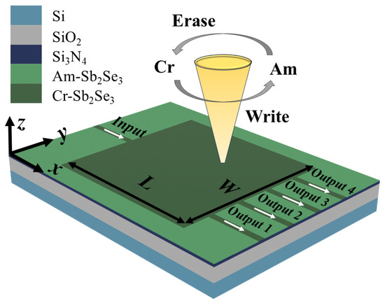
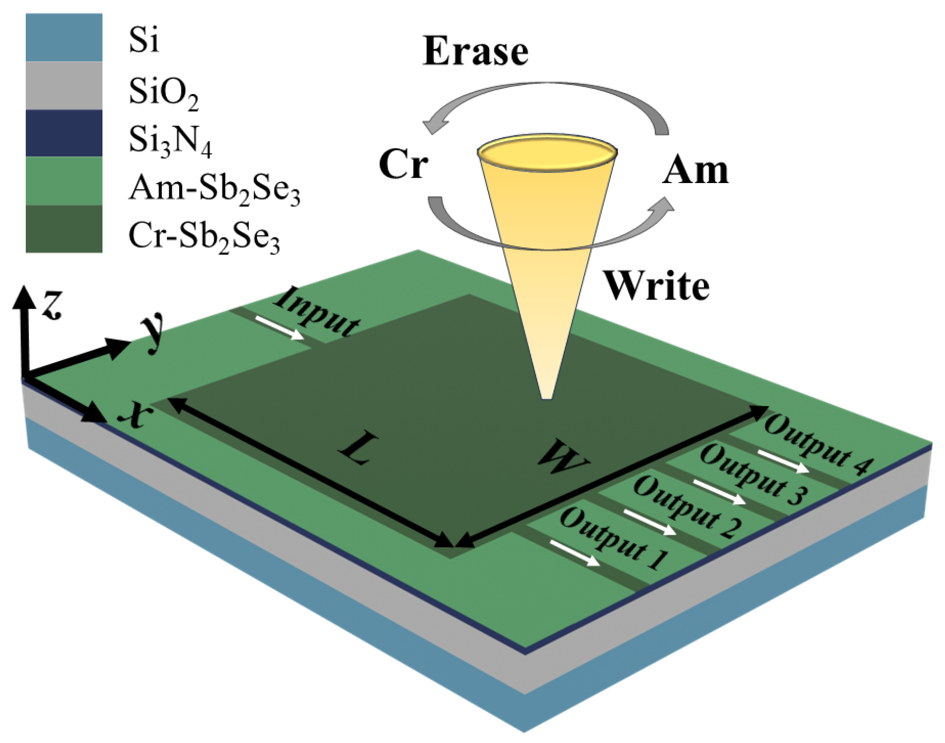
The proposed programmable multi-channel wavelength demultiplexers are realized on an etchless silicon nitride photonic platform integrated with the low-loss phase-change material Sb2Se3. The material stack of this platform is illustrated schematically in Figure 1. Starting from a silicon substrate, a 2 μm thick layer of silicon dioxide (SiO2) is employed as a lower cladding to optically isolate the waveguide mode from the substrate. A 400 nm thick stoichiometric silicon nitride (Si3N4) layer is deposited directly on top of the SiO2 buffer, serving as the passive waveguide core layer. Critically, the Si3N4 film remains entirely unetched throughout the entire device fabrication process, thereby eliminating sidewall roughness and its associated scattering losses. Above the Si3N4 core, a 50 nm thick film of Sb2Se3 is deposited through magnetron sputtering, which initially resides in an amorphous state. Finally, a thin encapsulation layer of SiO2 is applied over the Sb2Se3 surface to prevent oxidation or environmental degradation of the phase-change film during the subsequent laser-writing steps and device operation. Note that such SiO2 cladding also helps mitigate surface scattering loss of Sb2Se3 by burying the Sb2Se3 surface under a low-index dielectric, avoiding direct contract with the environment.
Figure 1.
Schematic illustration of the programmable multi-channel wavelength demultiplexer and the material stack. The device consists of one input waveguide, four parallel output waveguides, and a central design region (L = 24 µm, W = 24 µm). All waveguides have a uniform width of 1.0 µm and a center-to-center spacing of 5.0 µm. The material stack (from bottom to top) includes a silicon substrate, a 2 μm thick SiO2 lower cladding, a 400 nm thick unetched Si3N4 core layer, and a 50 nm thick Sb2Se3 phase-change film. For visual clarity, the top SiO2 encapsulation layer is omitted in the schematic.
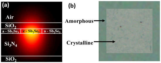
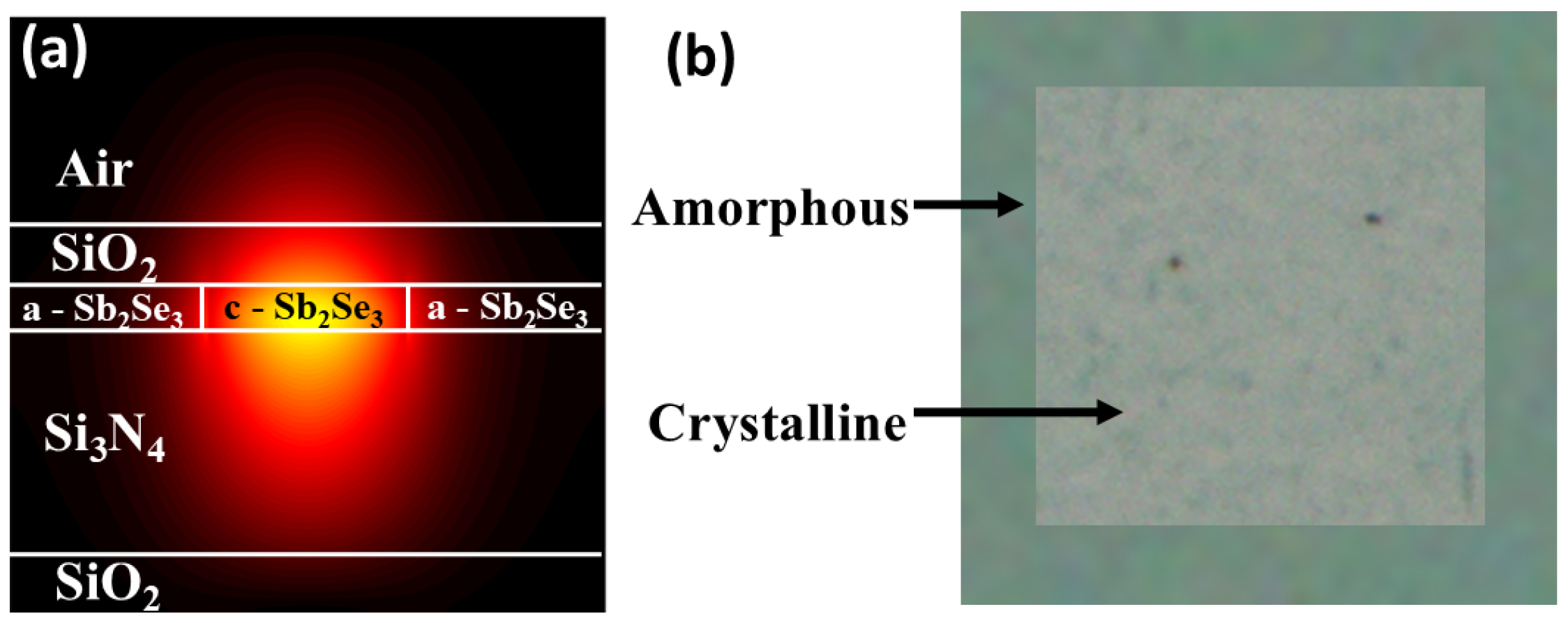
The fundamental device geometry consists of one input waveguide, four parallel output waveguides, and a central design region, as illustrated in Figure 1. All input and output waveguides are straight strip waveguides with a uniform width of 1.0 µm. As shown in Figure 2a, this waveguide configuration supports the fundamental transverse electric (TE0) mode, whose electric field profile is well confined within the waveguide core. The four output waveguides are spaced apart by a center-to-center distance of 5.0 µm. The central design region, where the wavelength-selective routing functionality is implemented, is a square area of length L = 24 µm and width W = 24 µm, with both dimensions indicated in Figure 1.
Figure 2.
(a) Simulated electric field profile of the fundamental transverse electric (TE0) mode supported by the 1.0 μm wide strip waveguide (c-Sb2Se3 region width). c-Sb2Se3 and a-Sb2Se3 represent crystalline and amorphous states of Sb2Se3 film, respectively. (b) Optical microscope image of the Sb2Se3 film, displaying the clear visual contrast between the crystalline and amorphous states.
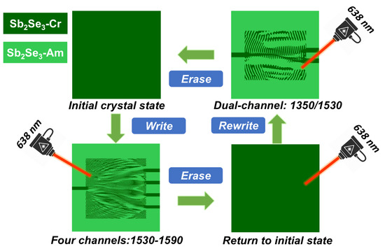
The operational function of the device is reconfigured by locally modifying the crystalline and amorphous states of the Sb2Se3 film within the central design region, thereby altering the spatial refractive index distribution. As shown in Figure 2b, the optical microscope image reveals the clear contrast between the crystalline and amorphous states of Sb2Se3. By reversibly switching the Sb2Se3 material between these two states through laser irradiation, different refractive index patterns can be defined in the design region. When a focused laser beam is scanned across the design area, the exposed amorphous Sb2Se3 is converted into the crystalline state along the written path, forming the high-index structures that route specific wavelengths to the corresponding output ports. To change the device functionality, the existing crystalline pattern is first erased via laser-induced re-amorphization, restoring the design region to a uniform amorphous state. A new pattern can then be written in the same location by repeating the laser-writing process with a different scanning trajectory. This “write–erase–rewrite” capability, illustrated schematically in Figure 1, enables distinct wavelength-routing functions, including four-channel demultiplexer, three-channel demultiplexer, two-channel demultiplexer, and single-wavelength router, to be dynamically interchanged on the identical physical device without any modification to the underlying fabricated chip.
Inverse design of the programmable multi-channel wavelength demultiplexer is carried out using a topology optimization approach implemented within an open-source LumOpt framework [11], which operates as a Python 3.6 wrapper for the Ansys Lumerical three-dimensional finite-difference time-domain (3D FDTD) solver (Ansys Lumerical 2023 R2.3) [32,33,34]. In the 3D FDTD simulations, the computational domain spans 25 µm in the x-direction, 25 µm in the y-direction, and 1 µm in the z-direction, with a uniform mesh size of dx = dy = dz = 50 nm employed across the entire simulation volume. The boundary conditions were set to perfectly matched layer in all spatial directions, with 8 layers at each boundary. The fundamental TE mode was launched as the input source, with a spatial extent of 3 µm in the y-direction and 0.8 µm in the z-direction to match the mode profile of the 1.0 μm wide input waveguide. During the optimization process, the design region of 24 × 24 μm2 is discretized into a rectilinear grid of design cells, each of which is permitted to evolve continuously between the amorphous and crystalline states of Sb2Se3. The optimization is driven by a gradient-based algorithm that leverages the adjoint method to efficiently compute the sensitivity of a user-defined figure of merit (FOM) with respect to the material distribution at every cell within the design volume [35,36]. For each target functionality—whether a multi-channel coarse wavelength demultiplexer or a single-wavelength router—the FOM is constructed to maximize the power coupled from the fundamental transverse electric (TE0) input mode to the designated output port across a set of 11 equally spaced wavelengths spanning a 10 nm bandwidth centered at the specified operating wavelength [36]. Specifically, the FOM is defined using a generalized p-norm formulation given by [37]
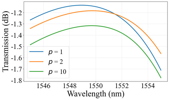
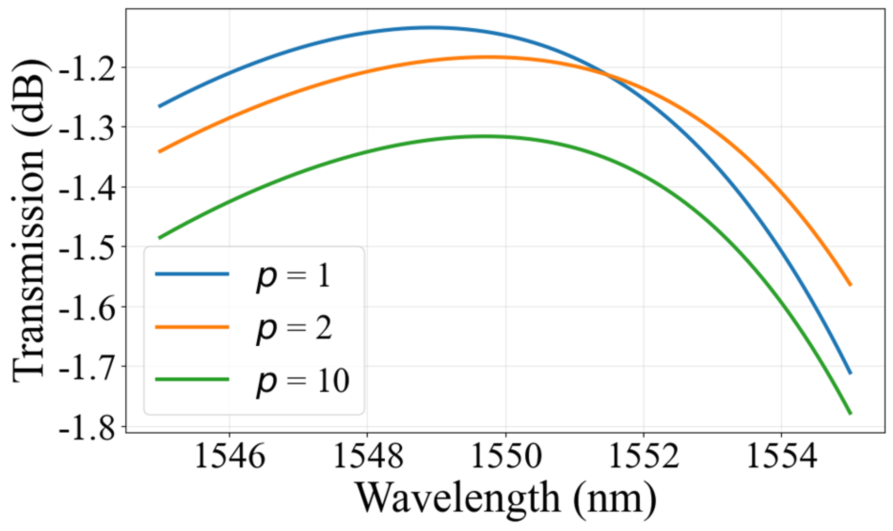
where T0 (λ) represents the target forward transmission spectrum, T(λ) is the actual mode expansion power transmission monitored at the designated output port, λ1 and λ2 define the lower and upper bounds of the wavelength range of interest, and p denotes the order of the generalized p-norm. It should be noted that the integration variable in this formulation is not a continuous wavelength variable but rather indexes the discrete wavelength sampling points within the optimization band, with a total of points uniformly spaced across the 10 nm bandwidth centered at each target wavelength. Correspondingly, the normalization factor is evaluated in its discretized form as , such that the integral effectively computes the arithmetic mean of the transmission performance across all sampled wavelengths. This ensures that the FOM represents a balanced spectral average over the entire band of interest, rather than an accumulated sum or a quantity dominated by any single wavelength [37]. In this work, the parameter p is set to 2, which corresponds to the Euclidean norm and effectively measures the root-mean-square deviation between the simulated and target transmission spectra. Compared to smaller p values that would overemphasize the center wavelength, or larger p values that would disproportionately penalize low-transmission wavelengths away from the center, p = 2 strikes a balanced trade-off across the 10 nm wavelength band, aiming to achieve uniformly high transmission (T) across the entire wavelength range. To quantitatively validate this choice, we selected the most complex device in our library—the four-channel demultiplexer operating at 1530–1590 nm—and focused on Output 2 (target wavelength 1550 nm) as the monitoring port. We ran the same inverse-design optimization for 16 iterations under p = 1, 2 and 10, keeping all other algorithmic parameters unchanged to ensure a single-variable comparison. As shown in Figure 3, p = 1 yields the highest peak transmission at 1550 nm among the three cases, but the transmission spectrum exhibits noticeable fluctuations across the 1545–1555 nm band, indicating that it overemphasizes the center wavelength at the expense of band-edge flatness. The curves for p = 2 and p = 10 are considerably smoother than that for p = 1, reflecting improved spectral uniformity. However, p = 10 imposes excessive uniformity, which overly constrains the optimization and leads to an overall reduction in transmission across the entire band. In contrast, p = 2 achieves the best balance between high peak transmission at the center wavelength and uniform transmission across the 10 nm bandwidth, confirming that p = 2 provides the optimal trade-off for our design objectives.
Figure 3.
Comparison of the optimized transmission spectra at Output 2 (target wavelength 1550 nm) of the four-channel demultiplexer (1530–1590 nm) obtained using different p-parameter values in the inverse-design optimization.
A series of forward and adjoint simulations are executed iteratively, with the material index in each cell updated according to the calculated gradients until the FOM converges to a stable optimum [5]. During the optimization, a minimum feature size of 200 nm was imposed to ensure compatibility with the laser-writing resolution. For the binarization and filtering strategy, a standard density-filtering and threshold projection scheme was employed. Specifically, a Gaussian filter with radius nm is first applied to the design variables to smooth the material distribution and prevent the formation of overly small or sharp features. A smoothed Heaviside projection with threshold is then applied to push the filtered design toward a binary distribution of purely amorphous and crystalline states. The projection steepness starts from an initial value of 1 and is progressively multiplied by 1.2 after each continuation stage to gradually enforce binarization. To quantitatively assess when the design has become sufficiently binary, a discreteness metric defined as is used, where is the design variable of the i-th grid cell and is the total number of cells. Binarization is considered converged when exceeds 0.99, indicating that the material distribution has been driven to a nearly binary state [36]. For the convergence criteria of the overall optimization, the optimizer (L-BFGS-B) terminates when either the relative function change falls below or the projected gradient norm drops below , with a maximum of 400 iterations per continuation stage. This inverse-design workflow enables the automatic generation of highly freeform geometries that efficiently route specific wavelengths to their assigned output channels while maintaining a compact device footprint compatible with the laser-induced phase change programming scheme [36].
3. Results and Discussion
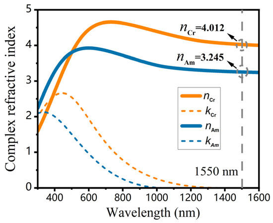
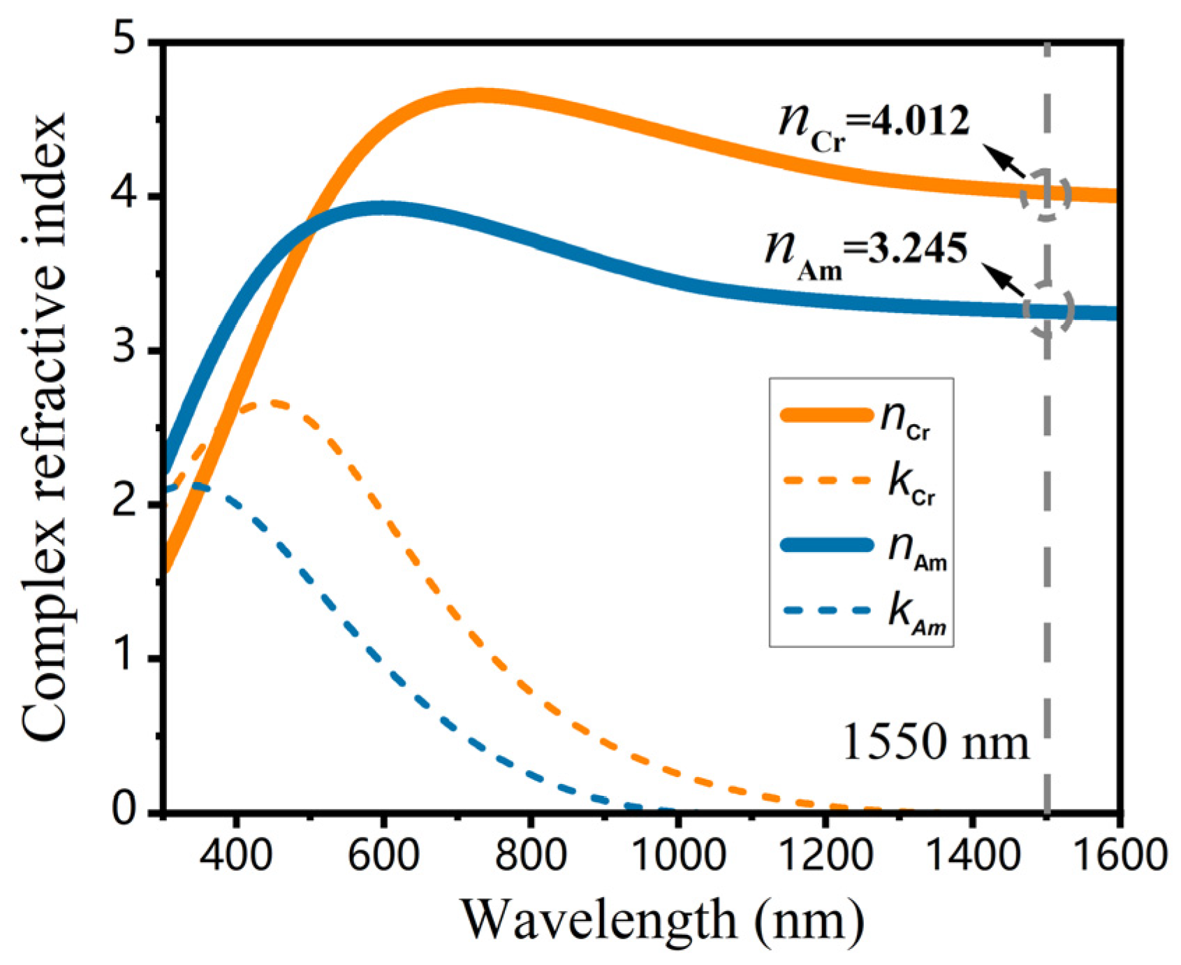
All the proposed devices share the same fundamental geometry illustrated in Figure 1 and are designed as programmable WDMs based on low-loss phase-change material platform. Refractive indices used in the design for Sb2Se3 are 4.012 in the crystalline state versus 3.245 in the amorphous state at λ = 1550 nm. The refractive indices of Sb2Se3 used in the simulations are based on experimental measurements conducted in our laboratory. As shown in Figure 4, the complex refractive index spectra of both amorphous and crystalline Sb2Se3 were characterized over the wavelength range of 300–1600 nm. In the wavelength range above 1300 nm, the imaginary part κ of the refractive index is negligibly small for both states, indicating that the material absorption loss is nearly zero and dispersion effects can be safely disregarded within the operating wavelength band of our devices. At the wavelength of λ = 1550 nm, the measured refractive indices are n = 4.012 for crystalline Sb2Se3 and n = 3.245 for amorphous Sb2Se3. A series of WDMs with different channel configurations (e.g., 1 × 2, 1 × 3, 1 × 4, and reconfigurable filters) were realized from the same base structure. Since the inverse design methodology has been detailed in the preceding section, it is not reiterated here. Instead, we present the simulated performance of these devices, including their spectral responses, electric field profiles at the operating wavelengths and FOM evolution curves during optimization processes [36].
Figure 4.
Complex refractive index spectra of Sb2Se3 in the amorphous and crystalline states over the wavelength range of 300–1600 nm, measured experimentally in our laboratory. The solid curves represent the real part n of the refractive index, and the dashed curves represent the imaginary part κ. In the spectra, the orange curves correspond to the crystalline state and the blue curves correspond to the amorphous state.
3.1. Single-Wavelength Router
Single-wavelength routers are designed to selectively route a specific target wavelength from the input waveguide to a designated output port while suppressing transmission to all other ports. Four independent devices are optimized for central wavelengths of 1530 nm, 1550 nm, 1570 nm, and 1590 nm, corresponding to output ports Output 1, Output 2, Output 3, and Output 4, respectively. For each device, the inverse design optimization targets the fundamental transverse electric (TE0) mode of the input waveguide as the input mode, and the same TE0 mode at the corresponding output port as the output mode. The FOM is constructed to maximize the power transmission to the intended output across an 11-wavelength set spanning a 10 nm bandwidth centered at the target wavelength.
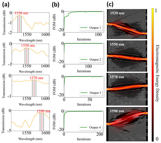
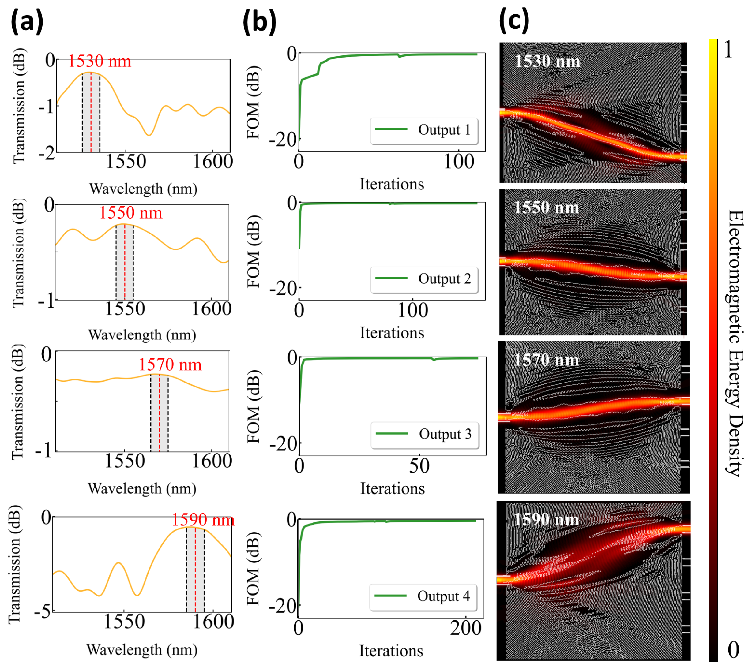
Figure 5a presents the simulated transmission spectra of four single-wavelength routers over the wavelength range from 1510 nm to 1610 nm, plotted as the transmission T for the respective target output port. Since each single-wavelength router is optimized independently for only one target wavelength, the design freedom is fully dedicated to maximizing the transmission over the 10 nm band centered at that wavelength. Consequently, when viewed over the broad 1510–1610 nm range, the transmission peak around the target wavelength is relatively modest and broad, with no sharp roll-offs. The wavelength selectivity remains low, as the device does not need to suppress transmission at other wavelengths.
Figure 5.
Single-wavelength routers optimized for central wavelengths of 1530 nm, 1550 nm, 1570 nm, and 1590 nm. (a) Simulated transmission spectra at the target output port for each device over the wavelength range from 1510 nm to 1610 nm. (b) Optimization trajectories showing the evolution of FOM to the target output port for each device. (c) Simulated electromagnetic energy density at the central wavelength of each channel. The white contour lines superimposed on the field plots indicate the boundaries of the inverse-designed crystalline Sb2Se3 patterns that define the waveguiding pathways within the central design region.
For the 1530 nm device, the simulated transmission efficiency at the central wavelength reaches −0.28 dB, with crosstalk to other output ports remaining below −33.57 dB over the entire 10 nm bandwidth (1525–1535 nm), and the average transmission efficiency is −0.30 dB. For the 1550 nm device, the simulated transmission efficiency at the central wavelength reaches −0.21 dB, with crosstalk to other output ports remaining below −32.03 dB over the 10 nm bandwidth (1545–1555 nm), with the average transmission efficiency is −0.22 dB. For the 1570 nm device, the simulated transmission efficiency at the central wavelength reaches −0.23 dB, with crosstalk to other output ports remaining below −30.58 dB over the 10 nm bandwidth (1565–1575 nm), and the average transmission efficiency is −0.24 dB. For the 1590 nm device, the simulated transmission efficiency at the central wavelength reaches −0.33 dB, with crosstalk to other output ports remaining below −32.63 dB over the 10 nm bandwidth (1585–1595 nm), and the average transmission efficiency is −0.36 dB. All four devices maintain transmission efficiencies above −0.33 dB at their respective target wavelengths, and they also exhibit consistently high average transmission across each designated 10 nm band.
The convergence behavior of the inverse design optimization is illustrated in Figure 5b, which shows the evolution of FOM as a function of the iteration number. For all four devices, the FOM exhibits a rapid increase during the initial iterations before gradually saturating toward a stable optimum, confirming the effectiveness of the gradient-based topology optimization approach.
Figure 5c displays the simulated electromagnetic energy density at the central wavelength of each channel for the four single-wavelength routers. The white contour lines superimposed on the field plots delineate the boundary of the optimized structure, clearly indicating the freeform crystalline Sb2Se3 patterns that define the waveguiding pathways responsible for routing each target wavelength to its designated output port.
Single-wavelength routers serve as the fundamental building blocks of programmable demultiplexer library. Their compact footprints and high wavelength selectivity validate the effectiveness of the inverse-design approach for PCM-based reconfigurable photonics.
3.2. Two-Wavelength Demultiplexer
Two-channel wavelength demultiplexer is optimized to separate input signals at 1550 nm and 1570 nm, directing the 1550 nm signal to Output 2 and the 1570 nm signal to Output 3. Inverse design process employs TE0 mode of the input waveguide as the input mode and the TE0 modes of the two designated output waveguides as the output modes. FOM is defined to simultaneously maximize the transmission from input to each target output across the 10 nm wavelength bands centered at 1550 nm and 1570 nm, respectively.
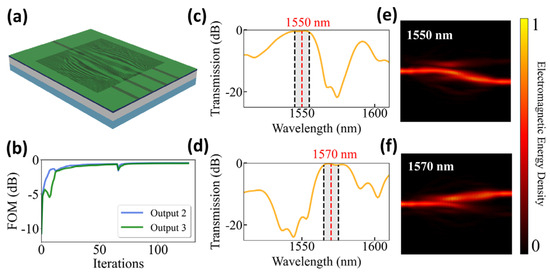
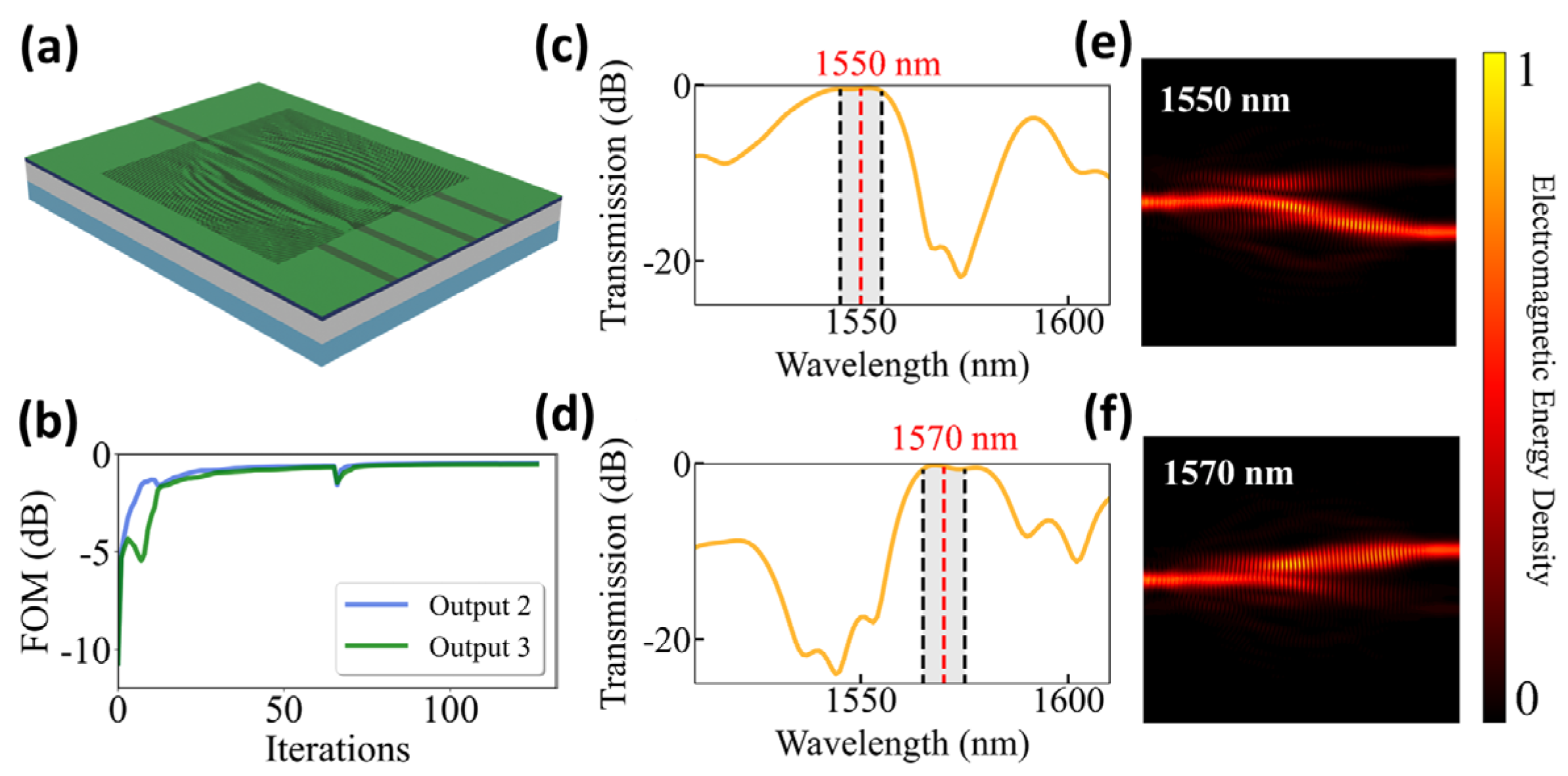
Figure 6a displays the structural layout of our designed two-channel demultiplexer, where the crystalline Sb2Se3 pattern within the 24 × 24 μm2 design region is clearly depicted. The pattern exhibits a non-intuitive, irregular geometry characteristic of topology-optimized designs, which enables efficient wavelength separation at 1550 nm and 1570 nm, respectively. Figure 6b traces the optimization trajectory of FOM for the two target output ports. The blue curve, corresponding to Output 2, rises rapidly during the initial iterations and subsequently saturates to a stable plateau. In contrast, the green curve for Output 3 exhibits a more complex evolution: after an initial rapid ascent, FOM experiences a temporary decline before recovering with a second steep rise and eventually converging to a stable optimum. Despite this non-monotonic behavior during the intermediate optimization stages, both channels ultimately achieve stable convergence, demonstrating the capability of the adjoint-based topology optimization framework to navigate complex design structures in multi-objective inverse design tasks.
Figure 6.
Two-channel demultiplexer optimized for target wavelengths of 1550 nm and 1570 nm. (a) Structural layout of the inverse-designed two-channel demultiplexer within the 24 × 24 μm2 central design region, where the crystalline Sb2Se3 pattern is indicated (dark region). (b) Optimization trajectories showing the evolution of FOM to Output 2 and Output 3. (c,d) Simulated transmission spectra at Output 2 and Output 3 over the wavelength range from 1510 nm to 1610 nm, showing the demultiplexing performance at 1550 nm and 1570 nm. (e,f) Simulated electromagnetic energy density at the central wavelengths of 1550 nm and 1570 nm, respectively.
Figure 6c,d present the simulated transmission spectra at Output 2 and Output 3 over the wavelength range from 1510 nm to 1610 nm. In the two-channel demultiplexer, optimization must simultaneously enforce high transmission at both 1550 nm and 1570 nm while suppressing crosstalk between them. This additional constraint sharpens the spectral response around each target wavelength compared to the single-channel case. When viewed over the 1510–1610 nm range, the transmission peaks at 1550 nm and 1570 nm become notably more pronounced, particularly on their adjacent sides—the right shoulder of the 1550 nm peak and the left shoulder of the 1570 nm peak—indicating improved wavelength selectivity and reduced inter-channel crosstalk.
Besides Output 2 and Output 3, the transmission to the remaining two output ports (Output 1 and Output 4) is also monitored to evaluate the crosstalk suppression across all four channels. At the central wavelength of 1550 nm, the transmission efficiency to Output 2 reaches −0.37 dB, with an average transmission efficiency of −0.42 dB over the 10 nm bandwidth (1545–1555 nm), while the crosstalk to Output 3 is suppressed to −17.18 dB, and the crosstalk to Output 1 and Output 4 are −39.03 dB and −37.78 dB. Conversely, at 1570 nm, the transmission to Output 3 is −0.36 dB, with an average transmission efficiency of −0.45 dB over its 10 nm bandwidth (1565–1575 nm), and the crosstalk to Output 2 is −18.20 dB, while the crosstalk to Output 1 and Output 4 are −36.15 dB and −36.69 dB. Figure 6e,f show the simulated electromagnetic energy density at the central wavelengths of 1550 nm and 1570 nm. At 1550 nm, the energy is primarily confined to the path leading to Output 2, while at 1570 nm, it is directed toward Output 3, confirming the wavelength-selective routing functionality.
3.3. Three-Channel Demultiplexer
Three-channel demultiplexer is designed to route input wavelengths of 1530 nm, 1550 nm, and 1570 nm to Output 1, Output 2, and Output 3, respectively. The optimization follows the same topology-optimization framework, with the FOM configured to maximize the power coupled from input TE0 mode to TE0 mode of each respective output port over 10 nm bandwidths centered at the three target wavelengths.
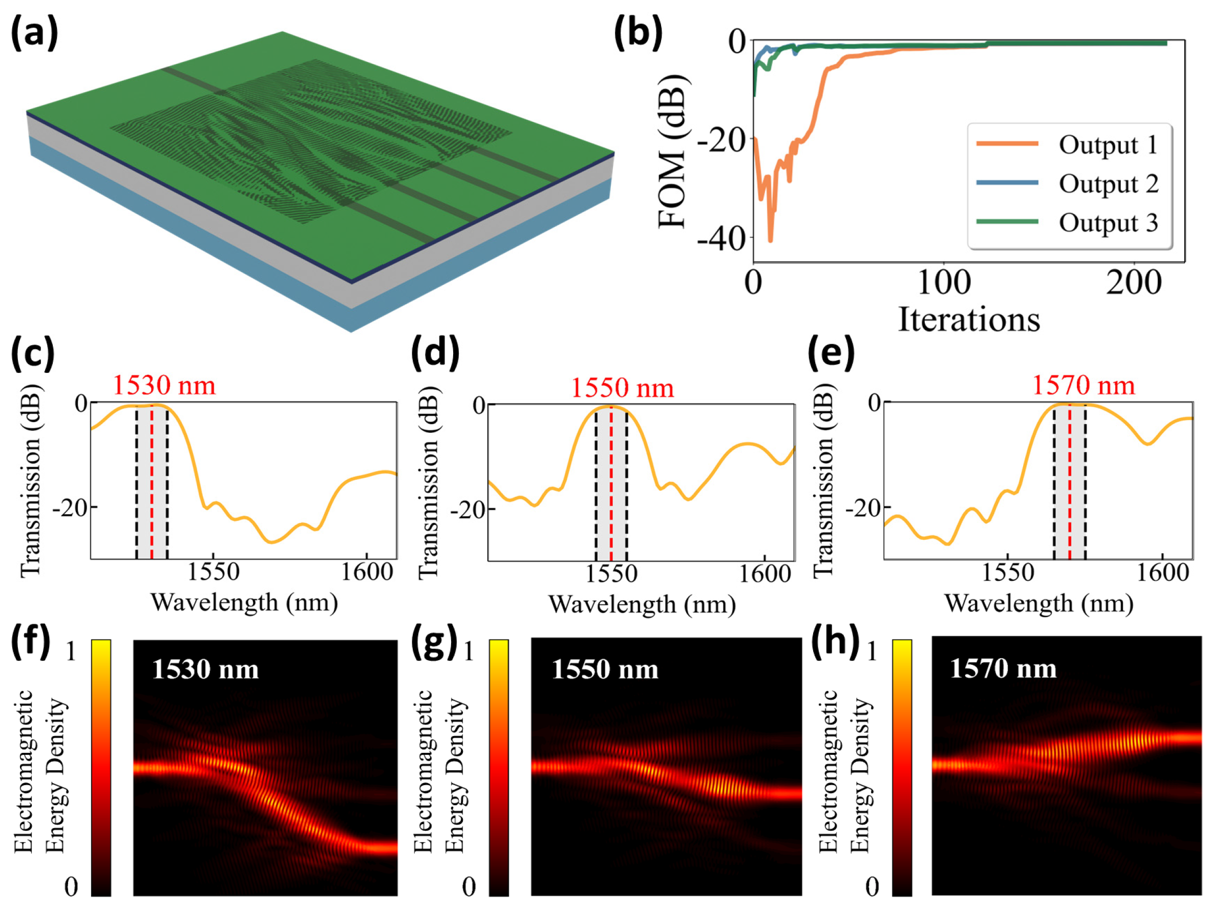
Figure 7a shows the structural layout of the three-channel demultiplexer, revealing the freeform crystalline Sb2Se3 pattern that defines the waveguiding network within the central design region. The non-intuitive geometry, automatically generated through the inverse-design process, efficiently routes the three target wavelengths to their respective output ports while maintaining a compact footprint identical to that of the single- and two-channel devices.
Figure 7.
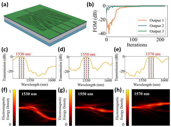
Three-channel demultiplexer optimized for target wavelengths of 1530 nm, 1550 nm, and 1570 nm. (a) Structural layout of the inverse-designed three-channel demultiplexer within the 24 × 24 μm2 central design region, where the crystalline Sb2Se3 pattern is indicated (dark region). (b) Optimization trajectories showing the evolution of FOM to Output 1, Output 2 and Output 3. (c–e) Simulated transmission spectra at Output 1, Output 2 and Output 3 over the wavelength range of 1510–1610 nm. (f–h) Simulated electromagnetic energy density at the central wavelengths of 1530 nm, 1550 nm, and 1570 nm, respectively.
The convergence behavior of inverse design optimization is illustrated in Figure 7b, which traces the evolution of FOM for the three target output ports as a function of the optimization iteration. The optimization trajectories for the three channels exhibit distinct evolutionary paths. The orange curve, corresponding to Output 1, undergoes an initial rapid decline, followed by a steep ascent before gradually saturating to a stable plateau. The blue curve for Output 2 rises rapidly during the early iterations and subsequently levels off to a steady optimum. The green curve, associated with Output 3, displays a more complex progression: after an initial rapid increase, the FOM experiences a moderate dip before recovering with a second rise and eventually converging to a stable value. Despite the increased complexity of simultaneously optimizing three independent wavelength-routing functions within the same compact design region, all three channels ultimately achieve stable convergence, demonstrating the robustness of the adjoint-based topology optimization framework for multi-objective inverse design.
Figure 7c–e present the simulated transmission spectra at Output 1, Output 2 and Output 3, respectively, over the wavelength range from 1510 nm to 1610 nm. With three wavelength channels sharing the same compact footprint, the optimization problem becomes more constrained. Each channel must not only achieve high transmission at its own center wavelength but also maintain deep rejection at the other two channel wavelengths. Consequently, the transmission peaks become even more pronounced than in the two-channel device.
Besides Output 1–3, the fundamental device geometry includes a fourth output waveguide (Output 4), which is not assigned as a target port in the three-channel demultiplexer; nevertheless, its crosstalk level is also evaluated. At the central wavelength of 1530 nm, the transmission efficiency to Output 1 reaches −0.56 dB, with an average transmission efficiency of −0.64 dB over the 10 nm bandwidth (1525–1535 nm); the crosstalk to Output 2 and Output 3 is suppressed to −15.66 dB and −26.18 dB, respectively, and the crosstalk to the unused Output 4 is −31.30 dB. At the central wavelength of 1550 nm, the peak transmission to Output 2 reaches −0.37 dB, with an average transmission efficiency of −0.66 dB over the 10 nm bandwidth (1545–1555 nm); the crosstalk to Output 1 and Output 3 is −19.02 dB and −16.50 dB, respectively, and the crosstalk to Output 4 is −32.29 dB. At the central wavelength of 1570 nm, the transmission to Output 3 is −0.49 dB, with an average transmission efficiency of −0.54 dB over the 10 nm bandwidth (1565–1575 nm); the crosstalk to Output 1 and Output 2 is suppressed to −26.22 dB and −14.67 dB, and the crosstalk to Output 4 is −31.84 dB.
Figure 7f–h display the simulated electromagnetic energy density at the central wavelengths of 1530 nm, 1550 nm, and 1570 nm, respectively. At 1530 nm, the energy is primarily confined to the path leading to Output 1; at 1550 nm, it is directed toward Output 2; and at 1570 nm, it is routed to Output 3. These energy density profiles directly confirm the wavelength-selective routing functionality achieved by the inverse-designed device.
3.4. Four-Channel Demultiplexer
Four-channel coarse wavelength-division demultiplexer is one of the most important device in the programmable library, which is designed to separate input signals at 1530 nm, 1550 nm, 1570 nm, and 1590 nm and route each wavelength to a distinct output port among the four available channels. Inverse design optimization employs the fundamental TE0 mode of input waveguide as the input mode and the TE0 modes of all four output waveguides as the output modes. FOM is constructed to simultaneously maximize the power transmission from the input to each of the four target output ports across their respective 10 nm bandwidths, evaluated over 11 equally spaced wavelength points centered at 1530 nm, 1550 nm, 1570 nm, and 1590 nm.
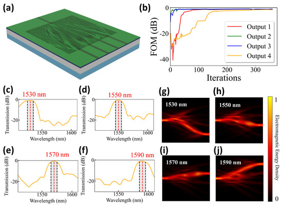
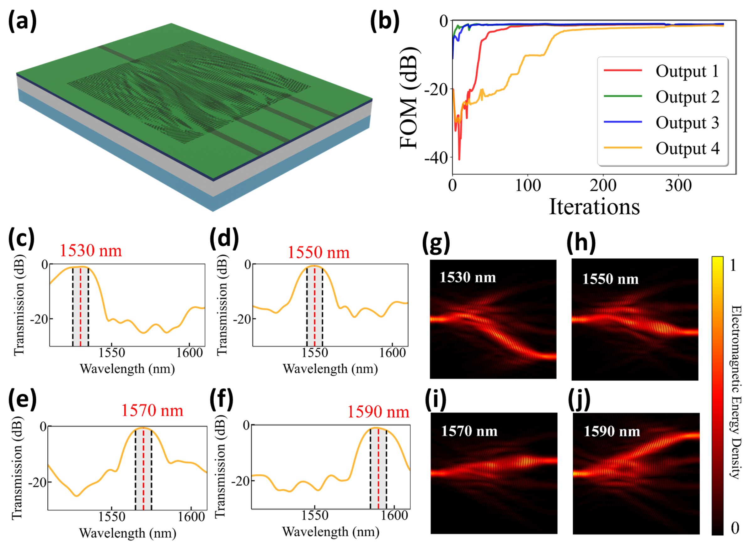
As presented in Figure 8a, four-channel demultiplexer incorporates a freeform crystalline Sb2Se3 pattern within the 24 × 24 μm2 central design region, generated by the inverse-design approach. Despite its more complex functionality, four-channel demultiplexer retains the same compact footprint as the single-, two-, and three-channel devices, and distributes the four target wavelengths to Outputs 1–4 with high selectivity. The convergence behavior of inverse design optimization is presented in Figure 8b, which traces the FOM of four target output ports. The green curve, corresponding to Output 2, rises rapidly during the initial iterations and subsequently levels off to a stable plateau. The blue curve, representing Output 3, also increases quickly at first, then experiences a moderate decline before rising again and eventually converging to a stable optimum. The red curve for Output 1 and the yellow curve for Output 4 share a similar pattern: both undergo an initial drop followed by a steep ascent, finally settling into a plateau. Despite the distinct evolutionary paths, all four channels achieve stable convergence, demonstrating the capability of the inverse design framework to handle the multi-wavelength routing within a single device.
Figure 8.
Four-channel demultiplexer optimized for target wavelengths of 1530 nm, 1550 nm, 1570 nm, and 1590 nm. (a) Structural layout of the inverse-designed device within the 24 × 24 μm2 central design region, where the crystalline Sb2Se3 pattern is indicated (dark region). (b) Optimization trajectories showing the evolution of FOM to the four target output ports. (c–f) Simulated transmission spectra at Output 1–4, respectively, over the wavelength range from 1510 nm to 1610 nm. (g–j) Simulated electromagnetic energy density at the central wavelengths of 1530 nm, 1550 nm, 1570 nm, and 1590 nm, respectively.
Simulated transmission spectra for the four output ports—Output 1 (1530 nm), Output 2 (1550 nm), Output 3 (1570 nm), and Output 4 (1590 nm)—over the wavelength range from 1510 nm to 1610 nm are presented in Figure 8c–f, respectively. In the four-channel demultiplexer, the inverse design algorithm faces the most stringent requirements: it must route four distinct wavelengths to four different output ports within the same 24 × 24 μm2 region while suppressing crosstalk among all combinations. This highly multi-objective constraint forces the optimizer to allocate the limited degrees of freedom extremely efficiently, resulting in the sharpest and most distinct spectral peaks among all devices when viewed over the 1510–1610 nm range. Each channel exhibits a narrow, well-defined passband with steep roll-offs on both sides, clearly separating the four target wavelengths. The progression from single- to four-channel devices demonstrates that increasing functional density sharpens the spectral selectivity, a direct consequence of the inverse design framework balancing multiple competing objectives.
At the central wavelength of 1530 nm, the transmission efficiency to Output 1 reaches −1.02 dB, with an average transmission efficiency of −1.12 dB over 1525–1535 nm; the crosstalk to Output 2, Output 3, and Output 4 is suppressed to −14.77 dB, −23.44 dB, and −22.22 dB, respectively. At the central wavelength of 1550 nm, the transmission efficiency to Output 2 reaches −0.65 dB, and the average transmission over 1545–1555 nm is −0.98 dB; the crosstalk to Output 1, Output 3, and Output 4 is suppressed to −19.64 dB, −15.02 dB, and −22.07 dB, respectively. At the central wavelength of 1570 nm, the transmission efficiency to Output 3 is −0.63 dB at its central wavelength, with an average of −0.94 dB over 1565–1575 nm; the crosstalk to Output 1, Output 2, and Output 4 is suppressed to −24.55 dB, −14.94 dB, and −19.19 dB, respectively. At the central wavelength of 1590 nm, the transmission efficiency to Output 4 is −1.21 dB, with an average of −1.48 dB over 1585–1595 nm; the crosstalk to Output 1, Output 2, and Output 3 is suppressed to −22.50 dB, −16.26 dB, and −11.52 dB, respectively. Figure 8g–j display the simulated electromagnetic energy density at the central wavelengths of 1530 nm, 1550 nm, 1570 nm, and 1590 nm, respectively. Four-channel demultiplexer demonstrates that the inverse-design methodology scales effectively to the full utilization of all four output ports without increasing the device footprint.
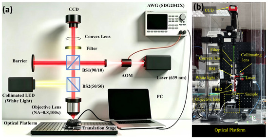
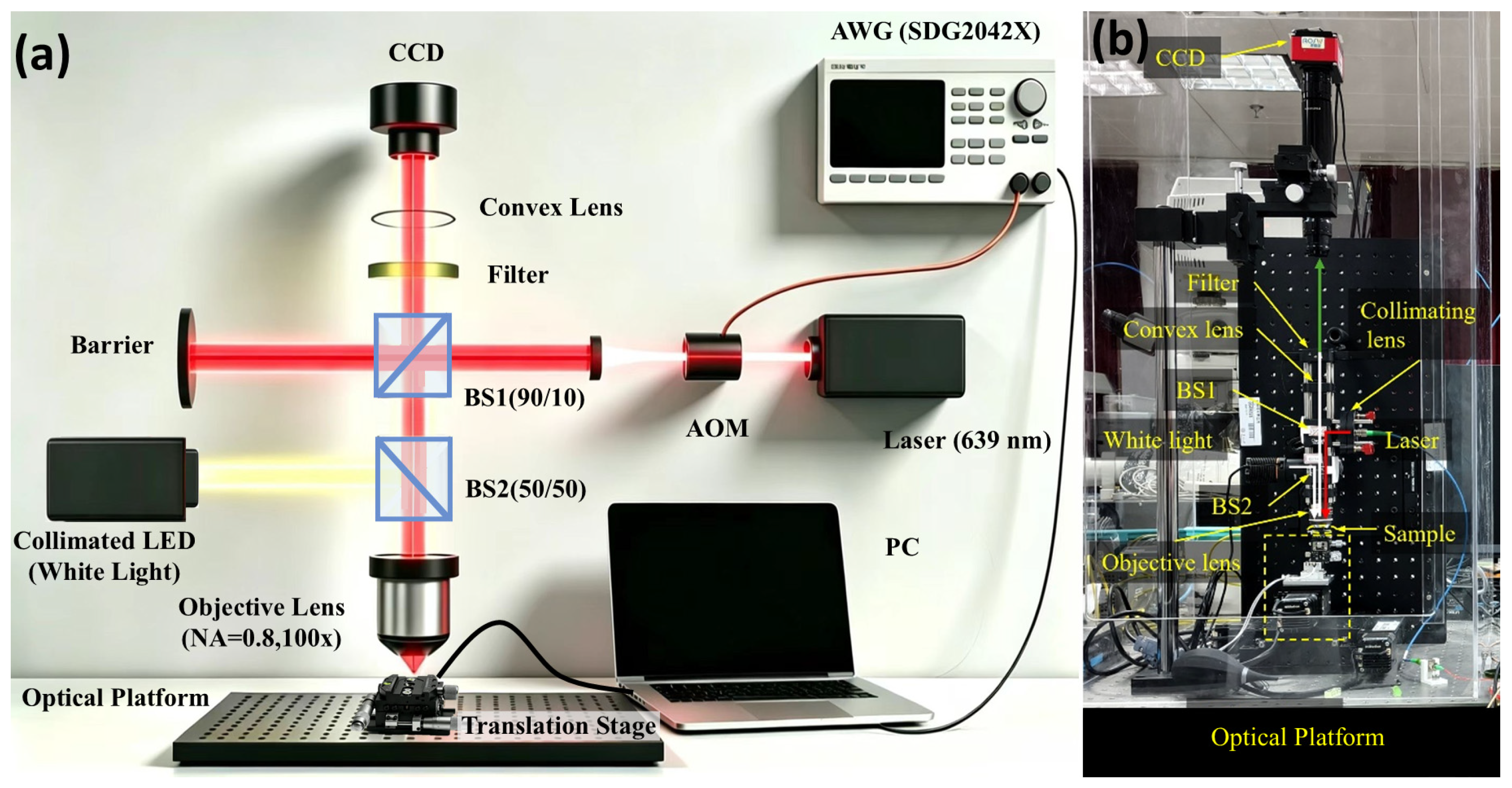
Figure 9 illustrates the fabrication platform used for all devices, where the schematic of laser-induced phase transition processing setup and actual equipment are included. A CW laser source with a wavelength of 639 nm is externally modulated by acoustic optical modulator (AOM) and enters into two beam splitters (BS1 and BS2). High numerical aperture objective lens (NA = 0.8, 100×) is further used to focus the laser on the chip sample, which is placed on the XYZ translation stage. Moreover, we have developed the system control software for the purpose of jointly controlling the AOM and XYZ translation stage. Using such fabrication equipment and control software, we can easily write or erase our designed structural patterns on the PCM film. In addition, such processing system that supports repeated rewriting is actually very suitable for the processing of inverse-designed wavelength demultiplexers here.
Figure 9.
Fabrication platform for the inverse-designed devices. (a) Schematic of the laser-writing setup illustrating the optical path. (b) Photograph of the fabrication equipment. BS: beam splitter, AWG: arbitrary waveform generator, AOM: acoustic optical modulator, PC: personal computer.
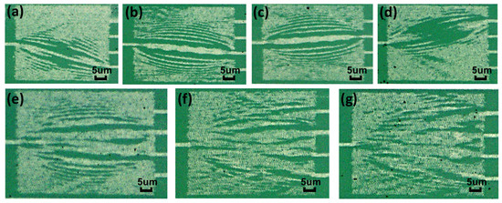
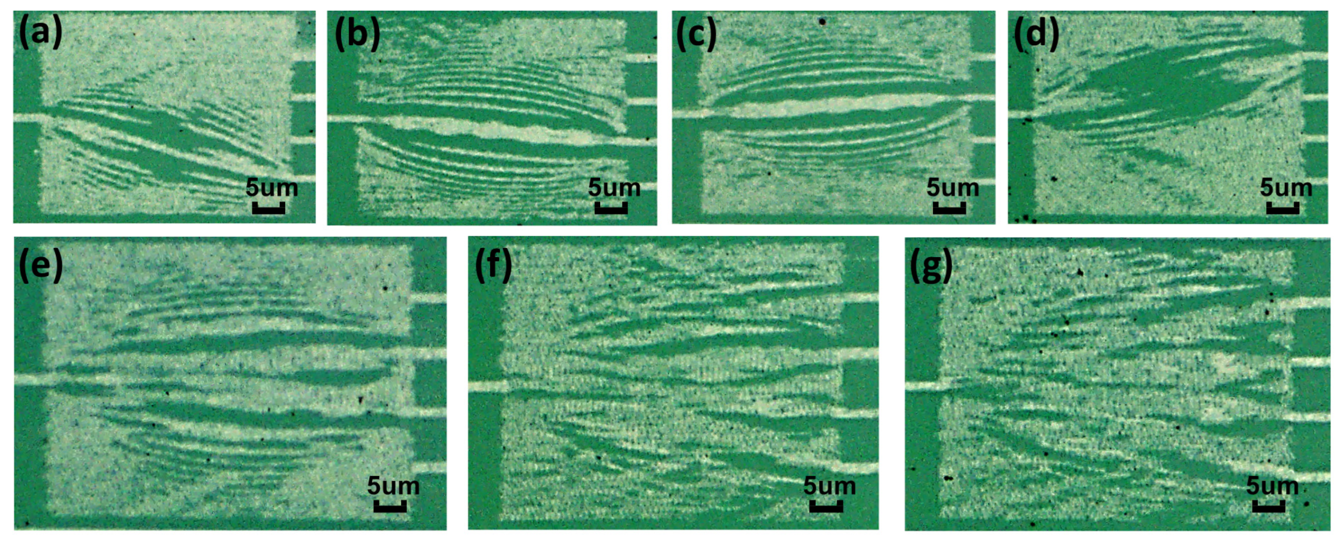
As shown in Figure 10a–g, we fabricate these aforementioned wavelength demultiplexers using our fabrication equipment and their optical microscope images are presented. These micrographs clearly display the actual top-down morphologies of the fabricated single-wavelength routers, as well as two-channel, three-channel, and four-channel wavelength demultiplexers, respectively. All images are presented in their original, unenhanced form, with 5 µm scale bars provided in each panel to allow readers to directly assess the feature dimensions. It should be noted that the fabricated devices have a very compact footprint of only 24 × 24 μm2, and during the inverse design optimization, a minimum feature size constraint of 200 nm was imposed on the structural patterns within the design region. Since these fine features already approach the diffraction-limited resolution of conventional optical microscopy, the sharpest edges and smallest gaps of the crystalline Sb2Se3 patterns cannot be fully resolved. Under these constraints, the images in Figure 10 represent the best achievable resolution with optical microscopy for devices of this size. Further improvement in imaging resolution would require the use of scanning electron microscopy (SEM), which we plan to pursue in future studies to provide even more detailed visualization of the fabricated structures. So, in the same design region, we can repeatedly write different structural patterns to achieve different device functions, corresponding to the programmable multi-channel wavelength demultiplexers.
Figure 10.
Optical microscope images of the fabricated devices. (a–d) Single-wavelength routers for 1530 nm, 1550 nm, 1570 nm, and 1590 nm, respectively. (e) Two-channel wavelength demultiplexer (1550/1570 nm). (f) Three-channel wavelength demultiplexer (1530/1550/1570 nm). (g) Four-channel wavelength demultiplexer (1530–1590 nm). All images are presented at the best achievable resolution of conventional optical microscopy.
To further illustrate this reconfigurability, we present a complete “write–erase–rewrite” cycle in Figure 11. The process begins with the Sb2Se3 film initially in the crystalline state across the entire wafer. In the first step (write), a focused laser beam from our home-built 638 nm laser-writing system is scanned across the design region according to the inverse-designed four-channel demultiplexer pattern. By applying a short write pulse of 500 ns duration at a power of 8.06 mW, the exposed crystalline Sb2Se3 is locally converted into the amorphous state, thereby defining the waveguiding structures that route the target wavelengths of 1530, 1550, 1570, and 1590 nm to their respective output ports. In the second step (erase), the same laser system is operated with a longer erase pulse of 5 ms duration at a lower power of 2.95 mW to induce recrystallization of the previously written amorphous regions, restoring the entire design area to the uniform crystalline state. In the third step (rewrite), a different inverse-designed pattern for a dual-band demultiplexer operating at 1310 and 1550 nm is written using the identical write pulse parameters, reconfiguring the device to perform an alternative wavelength-routing function. The entire cycle can be repeated multiple times without clear degradation: Sb2Se3-based thin-film devices with identical layer thickness have demonstrated over 2 × 10⁶ reversible write–erase cycles, maintaining approximately 21% transmission contrast with no material decomposition, bubbling, or delamination [15]. For pattern fidelity, our laser direct-writing system achieves a minimum spot size of 350 nm, adjustable according to feature sizes, ensuring faithful reproduction of the inverse-designed layouts. Regarding retention, Sb2Se3 is a non-volatile phase-change material that stably retains both amorphous and crystalline states at room temperature without external energy [15,16,17], and the 100 nm thick SiO2 encapsulation layer on our platform further prevents oxidation and selenium loss, enhancing long-term environmental stability. This demonstration validates the non-volatile and reversible programmability that distinguishes our platform from conventional static inverse-designed photonic circuits.
Figure 11.
Schematic of a complete “write–erase–rewrite” cycle on the Sb2Se3 phase-change platform.
3.5. Compact Dual-Band Demultiplexer for Cascaded Applications
To further demonstrate the versatility and scalability of the proposed processing platform, an additional two-channel wavelength demultiplexer operating at 1310 nm and 1550 nm was designed, targeting potential cascaded applications with previously described devices that operate in the C-band and adjacent bands. This dual-band demultiplexer shares the same fundamental waveguide configuration as the previous components, with input and output waveguides of 1.0 µm width, but employs a more compact optimization region measuring 10 × 8 μm2. Two output waveguides are arranged with a reduced center-to-center spacing of 2.0 µm, enabling an even smaller overall footprint suitable for dense on-chip integration.
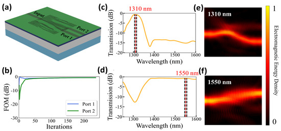
Figure 12a presents the structural layout of designed 1310/1550 nm dual-band demultiplexer within the compact design region, revealing the freeform crystalline Sb2Se3 pattern optimized for efficient separation of two widely spaced wavelength bands. The inverse design optimization follows the same topology-optimization framework, with the figure of merit configured to simultaneously maximize transmission to the two designated output ports, labeled as Port 1 and Port 2 in the figure, across 10 nm bandwidths centered at 1310 nm and 1550 nm.
Figure 12.
Two-channel dual-band demultiplexer optimized for target wavelengths of 1310 nm and 1550 nm. (a) Structural layout of the inverse-designed device within a compact 10 × 8 μm2 central design region, showing the freeform crystalline Sb2Se3 pattern. The input and output waveguides have a uniform width of 1.0 µm, and the two output ports, denoted as Port 1 and Port 2, are spaced by a center-to-center distance of 2.0 µm. (b) Optimization trajectory showing the evolution of FOM to Port 1 and Port 2. (c,d) Simulated transmission spectra at Port 1 and Port 2 over the wavelength range from 1250 nm to 1600 nm. (e,f) Simulated electromagnetic energy density at the central wavelengths of 1310 nm and 1550 nm.
Figure 12b plots the FOM optimization trajectories for the two output channels. The blue curve corresponding to Port 1 rises sharply at the initial stage, decreases slightly afterward, and finally converges to a stable plateau. By contrast, the green curve for Port 2 drops steeply first, followed by a rapid upward trend, and eventually reaches a steady convergence state. The simulated transmission spectra at Port 1 and Port 2 are shown in Figure 12c,d, respectively, over a broad wavelength range from 1250 nm to 1600 nm. For Port 1, which is designed to route the 1310 nm signal, a relatively narrow and well-defined transmission peak is observed around the target wavelength. The transmission remains low on the longer wavelength side: above 1400 nm, the signal level falls to approximately −15 dB, indicating effective rejection of the C-band light. In contrast, Port 2—intended for the 1550 nm channel—exhibits a broad transmission band spanning from approximately 1400 nm to 1600 nm, with uniformly high efficiency across most of this range. Near 1310 nm, however, the transmission at Port 2 drops significantly, remaining below −10 dB, thereby providing sufficient isolation from the O-band input. These complementary spectral responses confirm that the dual band demultiplexer successfully separates the 1310 nm and 1550 nm signals while maintaining a compact footprint.
For the 1310 nm channel (O-band), the transmission efficiency at Port 1 reaches −0.64 dB at the central wavelength, with an average transmission of −0.66 dB over the 10 nm bandwidth (1305–1315 nm). The crosstalk from the 1310 nm input to Port 2 mains below −11.93 dB. For the 1550 nm channel (C-band), the transmission at Port 2 is −0.58 dB at the central wavelength, with an average of −0.58 dB over the 10 nm bandwidth (1545–1555 nm), while the crosstalk to Port 1 is suppressed to −13.96 dB. Figure 12e,f depict the simulated electromagnetic energy density at 1310 nm and 1550 nm, respectively.
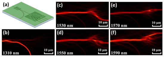
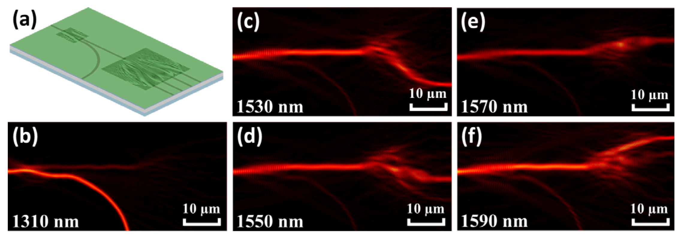
To simultaneously handle O-band signals and the more densely spaced C-band channels on the same chip, we cascade the dual-band demultiplexer with the aforementioned four-channel demultiplexer covering the C band and adjacent bands. As illustrated in Figure 13a, the hierarchical architecture consists of a front-end 1310/1550 nm splitter followed by the programmable 24 × 24 μm2 four-channel demultiplexer. The input signal is first injected into the dual band device: the 1310 nm wavelength is routed directly to Port 1, while the longer wavelengths (1530–1590 nm) are directed to Port 2. The output from Port 2 then feeds into the four channel demultiplexer, which separates the 1530 nm, 1550 nm, 1570 nm, and 1590 nm signals to Outputs 1, 2, 3, and 4, respectively. Figure 13b–f present the simulated electromagnetic energy density at five representative wavelengths: 1310 nm exiting from Port 1, 1530 nm at Output 1, 1550 nm at Output 2, 1570 nm at Output 3, and 1590 nm at Output 4. These field plots confirm that the cascaded network successfully routes each wavelength to its designated output port with low loss and minimal crosstalk. The hierarchical architecture thus demonstrates the scalability of the inverse-designed phase-change platform for constructing complex, reconfigurable wavelength-routing networks.
Figure 13.
Cascaded integration of the dual-band demultiplexer with the programmable multi-channel demultiplexer covering the C-band and adjacent bands. (a) Schematic of the hierarchical wavelength-routing network. (b–f) Simulated electromagnetic energy density at the input of the cascaded system for 1310 nm (routed to Port 1), 1530 nm (Output 1), 1550 nm (Output 2), 1570 nm (Output 3), and 1590 nm (Output 4), respectively.
3.6. Comparative Analysis and Robustness Evaluation
To comprehensively position our work within the current research landscape, we conduct a comparative analysis against representative inverse-designed wavelength demultiplexers, reconfigurable devices based on PCM, and dynamic metasurface platforms. The comparison is quantitatively summarized in Table 1, which benchmarks key performance metrics including platform, design method, reconfigurability, functionality, insertion loss, crosstalk, and footprint.
Table 1.
Performance comparison of inverse-designed wavelength demultiplexers and reconfigurable devices.
As shown in Table 1, our work occupies a distinctive position in the literature. Compared to the static inverse-designed four-channel Si3N4 CWDM by Pita Ruiz et al. [31] and the two-channel SOI demultiplexer by Piggott et al. [14], our devices achieve competitive insertion loss and crosstalk suppression within the same footprint, while additionally offering non-volatile reconfigurability enabled by the low-loss phase-change material Sb2Se3—a capability that static devices inherently lack. Relative to PCM-based reconfigurable devices on SOI platforms, such as the mode converter and optical switch by Wei et al. [30] and the directional coupler switch by Fang et al. [28], our work is the first to demonstrate inverse-designed programmable multi-channel wavelength demultiplexing on an etchless silicon nitride platform integrated with the low-loss Sb2Se3, supporting up to four independent wavelength channels from a single 24 × 24 µm2 structure. Furthermore, compared to dynamic metasurface platforms [38,39,40] that excel in reflection modulation, beam steering, and color display, our device targets a different application domain—programmable on-chip wavelength routing—and offers the unique advantage of programmable switching among 1-, 2-, 3-, and 4-channel demultiplexing functions. This combination of compact footprint, multi-channel operation, low insertion loss, and reversible programmability clearly highlights the advancement of our work.
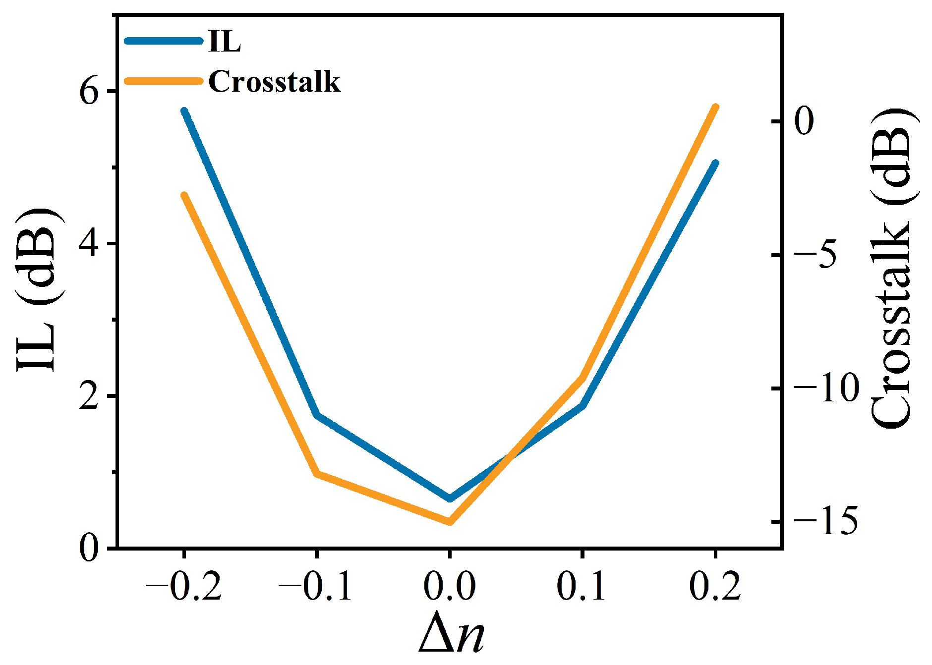
To assess the robustness of our inverse-designed devices under practical fabrication and material uncertainties, we performed a systematic tolerance study. We selected the most complex device—the four-channel demultiplexer operating at 1530–1590 nm—as the primary test vehicle. All tolerance simulations focused on Output 2 (target wavelength 1550 nm) and evaluated the peak insertion loss at 1550 nm and the worst crosstalk to the other output ports.
Regarding Sb2Se3 thickness variation, we evaluated its impact on device performance through 3D FDTD simulations. The results indicate that the device performance is highly sensitive to thickness variations, with a relatively small tolerance window. This sensitivity arises because the guided optical mode is strongly influenced by the Sb2Se3 layer thickness. However, the Sb2Se3 film in our platform is deposited via magnetron sputtering, a technique known for its excellent thickness uniformity and nanometer-scale precision. This ensures that the nominal 50 nm thickness can be accurately maintained across the entire wafer, thereby effectively mitigating the risk of performance degradation due to thickness deviations in practical fabrication.
Regarding refractive index variation, because our platform uses a long-duration annealing step that guarantees the entire film is initially fully crystalline, the crystalline-state refractive index is precisely controlled without deviation. The only possible uncertainty arises from incomplete amorphization during the short write pulse, which may leave some regions partially crystalline. We therefore exclusively considered variations in the amorphous-state refractive index by ±0.1 and ±0.2 from its nominal value. The results are presented in Figure 14.
Figure 14.
Tolerance analysis of the four-channel demultiplexer (1530–1590 nm) at Output 2 (target wavelength 1550 nm) under amorphous-state Sb2Se3 refractive index variation.
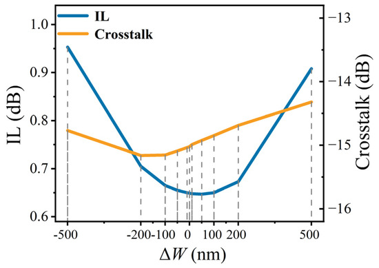
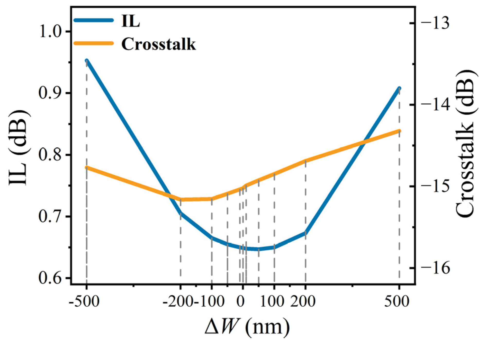
For laser-writing edge roughness, we note that both the length and width dimensions of the inverse-designed pattern can in principle be affected by fabrication variations. However, during the line-by-line writing process, the positions of individual points along the length direction are accurately controlled by the continuous stage motion, while the slight misalignment between adjacent lines introduced by the stage step in the width direction, together with the longitudinal positional deviation between the start and end points within each line, jointly contribute to fabrication deviations predominantly in the width direction. The length dimension can therefore be considered accurate and its deviation negligible. Focusing on the width direction, the point-by-point writing nature on non-regular freeform geometries means that the structural boundaries are inherently defined by the discrete laser spot positions. Local edge roughness therefore manifests as sub-wavelength-scale random width variations along the boundaries. Since these random deviations are statistically equivalent to a systematic width offset in terms of their cumulative impact on the guided optical mode, we evaluate the overall effect of edge roughness through the width-deviation tolerance analysis, with results presented in Figure 15.
Figure 15.
Tolerance analysis of the four-channel demultiplexer (1530–1590 nm) at Output 2 (target wavelength 1550 nm) under width variations (ΔW).
Regarding temperature drift, the writing process is performed with fully fixed parameters: the laser power is set at a constant 8.06 mW, the pulse duration is fixed at 500 ns, and the focal spot is precisely positioned at each point according to the predetermined pattern coordinates. Moreover, the Sb2Se3 film thickness is uniformly 50 nm across the entire wafer. Under these well-defined and repeatable conditions, the local heating at each writing point is highly reproducible, and the resulting temperature variation from point to point is negligible.
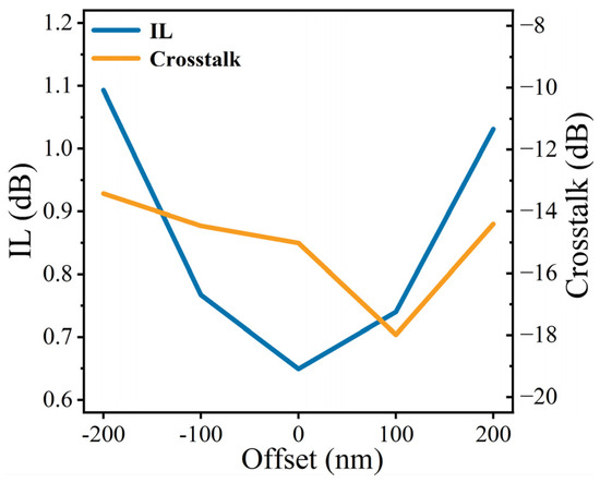
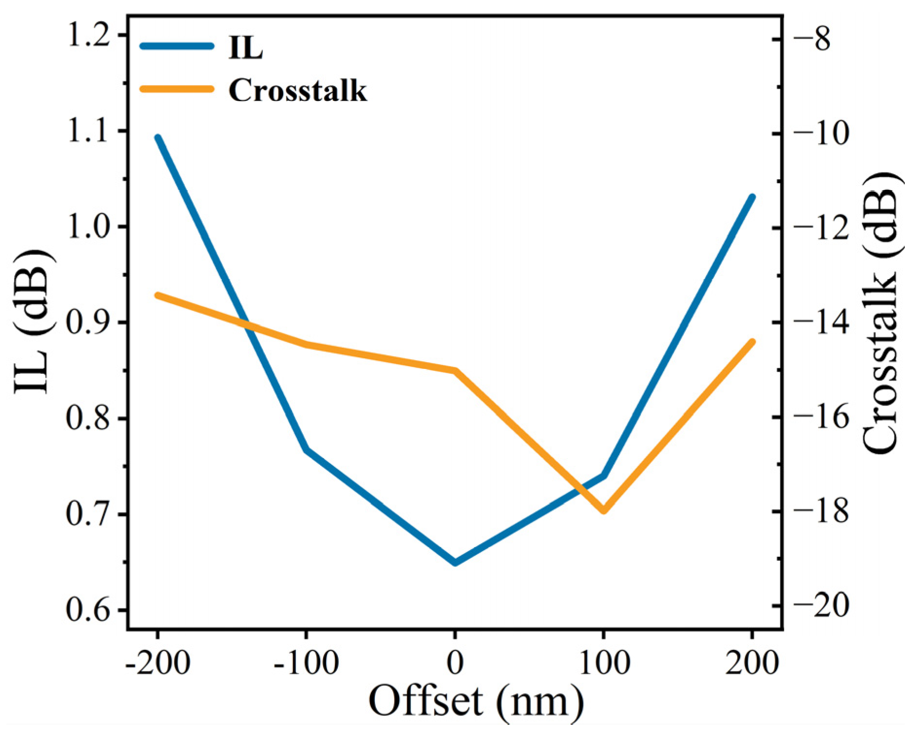
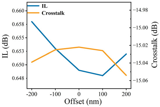
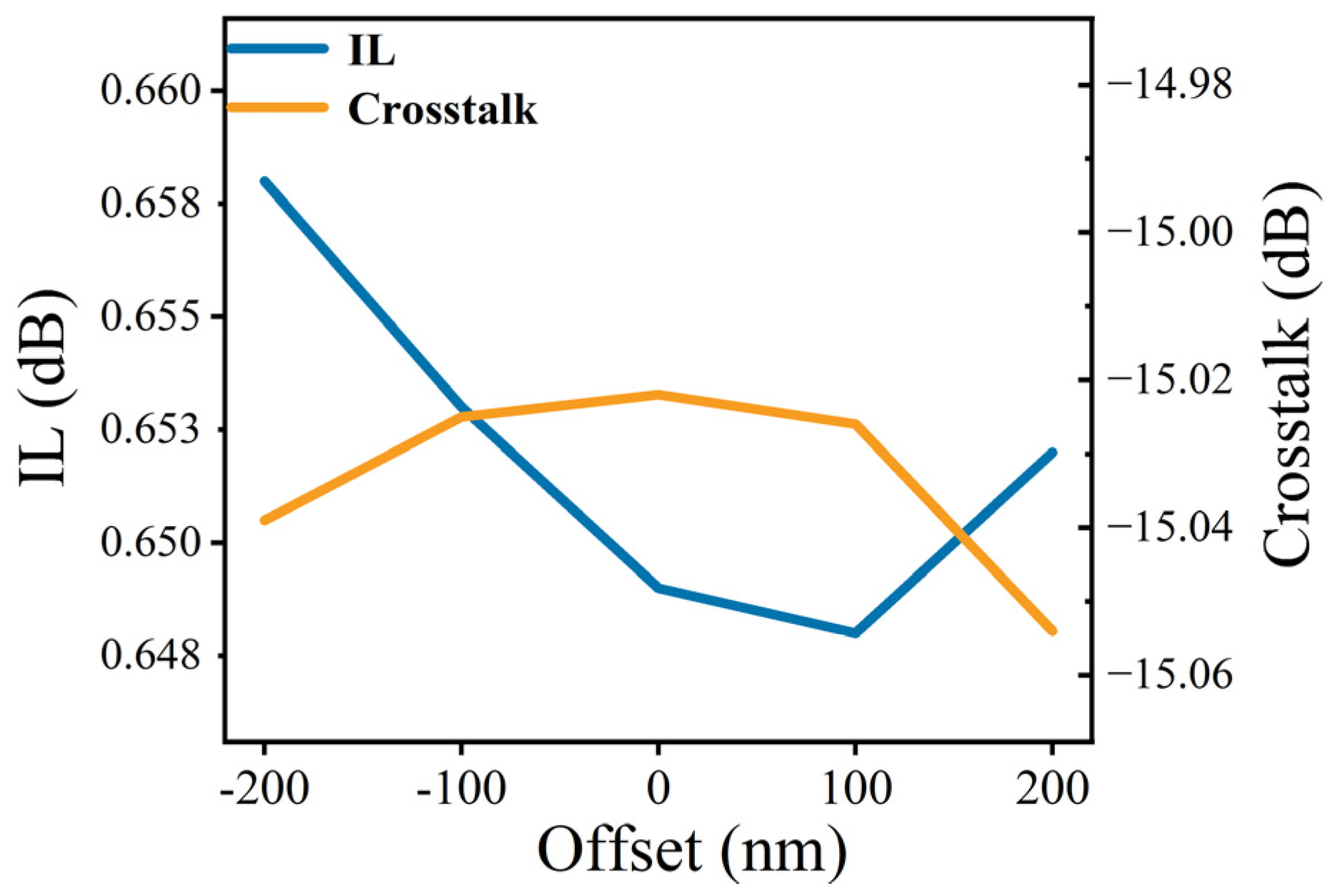
Finally, for input/output alignment errors, we introduced deliberate offsets of ±0.1 µm and ±0.2 µm to the input waveguide position and to the Output 2 waveguide position, respectively. The corresponding results are presented in Figure 16 and Figure 17.
Figure 16.
Tolerance analysis of the four-channel demultiplexer (1530–1590 nm) at Output 2 (target wavelength 1550 nm) under Input waveguide alignment offset.
Figure 17.
Tolerance analysis of the four-channel demultiplexer (1530–1590 nm) at Output 2 (target wavelength 1550 nm) under Output 2 waveguide alignment offset.
Overall, the comprehensive tolerance analysis demonstrates that our inverse-designed devices exhibit satisfactory robustness against a wide range of fabrication and material uncertainties. The combination of competitive performance metrics, reconfigurable multi-channel operation, and verified fabrication tolerance positions our phase-change-material-based platform as a promising candidate for next-generation programmable photonic integrated circuits.
4. Conclusions
In summary, we have proposed and numerically demonstrated a library of compact, freeform wavelength demultiplexers—including single-wavelength routers and two-, three-, and four-channel coarse wavelength-division demultiplexers—implemented on an etchless silicon nitride platform integrated with the low-loss phase-change material Sb2Se3. Using topology optimization (LumOpt) with a figure of merit evaluated over a 10 nm bandwidth, non-intuitive device geometries are automatically generated within a compact 24 × 24 μm2 design region, achieving low insertion loss (peak transmission > −1.21 dB) and suppressed crosstalk (<−11.52 dB) across all output channels. The common input/output port configuration enables post-fabrication reconfigurability via laser-induced write–erase–rewrite operation on the Sb2Se3 layer, overcoming the static functionality of conventional etched photonic circuits. Building on this library, we further demonstrate a dual-band (O-band and C-band) two-channel device that can be cascaded with the multi-channel demultiplexer covering the C band and adjacent bands (1525–1595 nm) to form a hierarchical wavelength-routing network. The combination of compact footprints, reconfigurability, and compatibility with both O-band and C-band (and adjacent bands) operation positions this technology as a promising candidate for next-generation software-defined optical interconnects and reconfigurable wavelength-division multiplexing systems.
Author Contributions
Conceptualization, P.Z.; methodology, P.Z., X.S., Z.L., Y.X. (Yiwen Xue), Y.L., Y.S., L.G., M.Y., L.Z. and Y.G.; investigation, P.Z. and Y.X. (Yin Xu); writing—original draft preparation, P.Z. and Y.X. (Yin Xu); writing—review and editing, all authors; supervision, Y.X. (Yin Xu); project administration, Y.X. (Yin Xu) and H.B. All authors have read and agreed to the published version of the manuscript.
Funding
This research was funded by National Natural Science Foundation of China, grant number 62205129, and Research Foundation of Engineering Research Center of Digital Imaging and Display, Ministry of Education, Soochow University, grant number ZZ2402.
Institutional Review Board Statement
Not applicable.
Informed Consent Statement
Not applicable.
Data Availability Statement
The data that support the findings of this study are available from the corresponding author upon reasonable request.
Conflicts of Interest
The authors declare no conflicts of interest.
References
- Shi, Y.; Zhang, Y.; Wan, Y.; Yu, Y.; Zhang, Y.; Hu, X.; Xiao, X.; Xu, H.; Zhang, L.; Pan, B. Silicon photonics for high-capacity data communications. Photon. Res. 2022, 10, A106. [Google Scholar] [CrossRef]
- Siew, S.Y.; Li, B.; Gao, F.; Zheng, H.Y.; Zhang, W.; Guo, P.; Xie, S.W.; Song, A.; Dong, B.; Luo, L.W.; et al. Review of silicon photonics technology and platform development. J. Light. Technol. 2021, 39, 4374–4389. [Google Scholar] [CrossRef]
- Xie, Y.; Wu, J.; Hong, S.; Wang, C.; Liu, S.; Li, H.; Ju, X.; Ke, X.; Liu, D.; Dai, D. Towards large-scale programmable silicon photonic chip for signal processing. Nanophotonics 2024, 13, 2051–2073. [Google Scholar] [CrossRef]
- Kim, J.; Kim, J.; Kim, J.; Hyeong, Y.; Neseli, B.; You, J.; Shim, J.; Shin, J.; Park, H.; Kurt, H. Inverse design of nanophotonic devices enabled by optimization algorithms and deep learning: Recent achievements and future prospects. Nanophotonics 2025, 14, 121–151. [Google Scholar] [CrossRef] [PubMed]
- Pan, Z.; Pan, X. Deep learning and adjoint method accelerated inverse design in photonics: A review. Photonics 2023, 10, 852. [Google Scholar] [CrossRef]
- Schul, L.; Mason, S.; Eun, S.; Ahn, G.H.; Vučković, J. Inverse design for scalable photonic systems. Nat. Rev. Mater. 2026. [Google Scholar] [CrossRef]
- Andonegui, I.; Calvo, I.; Garcia-Adeva, A.J. Inverse design and topology optimization of novel photonic crystal broadband passive devices for photonic integrated circuits. Appl. Phys. A 2014, 115, 433–438. [Google Scholar] [CrossRef]
- Piggott, A.Y.; Ma, E.Y.; Su, L.; Ahn, G.H.; Sapra, N.V.; Vercruysse, D.; Netherton, A.M.; Khope, A.S.P.; Bowers, J.E.; Vučković, J. Inverse-designed photonics for semiconductor foundries. ACS Photonics 2020, 7, 569–575. [Google Scholar] [CrossRef]
- Mao, S.; Cheng, L.; Zhao, C.; Khan, F.N.; Li, Q.; Fu, H.Y. Inverse design for silicon photonics: From iterative optimization algorithms to deep neural networks. Appl. Sci. 2021, 11, 3822. [Google Scholar] [CrossRef]
- Liao, J.; Tian, Y.; Yang, Z.; Xu, H.; Tang, C.; Wang, Y.; Zhang, X.; Kang, Z. Inverse design of highly efficient and broadband mode splitter on SOI platform. Chin. Opt. Lett. 2024, 22, 011302. [Google Scholar] [CrossRef]
- Christiansen, R.E. Inverse design of optical mode converters by topology optimization: Tutorial. J. Opt. 2023, 25, 083501. [Google Scholar] [CrossRef]
- Du, T.; Peng, Z.; Huang, P.; Zhang, Z.; Ma, H.; Jiang, X.; Huang, J.; Luo, M.; Zou, H.; Yang, J. Polygon search algorithm for ultra-compact multifunctional integrated photonics design. Photon. Res. 2024, 12, 1527. [Google Scholar] [CrossRef]
- Frandsen, L.H.; Sigmund, O. Inverse Design Engineering of All-Silicon Polarization Beam Splitters; Adibi, A., Lin, S.-Y., Scherer, A., Eds.; SPIE: San Francisco, CA, USA, 2016; p. 97560Y. [Google Scholar]
- Piggott, A.Y.; Lu, J.; Lagoudakis, K.G.; Petykiewicz, J.; Babinec, T.M.; Vučković, J. Inverse design and demonstration of a compact and broadband on-chip wavelength demultiplexer. Nat. Photonics 2015, 9, 374–377. [Google Scholar] [CrossRef]
- Wuttig, M.; Bhaskaran, H.; Taubner, T. Phase-change materials for non-volatile photonic applications. Nat. Photonics 2017, 11, 465–476. [Google Scholar] [CrossRef]
- Wu, C.; Jiao, Z.; Deng, H.; Huang, Y.-S.; Yu, H.; Takeuchi, I.; Ríos Ocampo, C.A.; Li, M. Reconfigurable inverse-designed phase-change photonics. APL Photonics 2025, 10, 016113. [Google Scholar] [CrossRef]
- Fang, Z.; Chen, R.; Zheng, J.; Majumdar, A. Non-volatile reconfigurable silicon photonics based on phase-change materials. IEEE J. Sel. Top. Quantum Electron. 2022, 28, 8200317. [Google Scholar] [CrossRef]
- Prabhathan, P.; Sreekanth, K.V.; Teng, J.; Ko, J.H.; Yoo, Y.J.; Jeong, H.-H.; Lee, Y.; Zhang, S.; Cao, T.; Popescu, C.-C.; et al. Roadmap for phase change materials in photonics and beyond. iScience 2023, 26, 107946. [Google Scholar] [CrossRef]
- Saha, N.; Brunetti, G.; Ciminelli, C. Highly efficient phase change material assisted reconfigurable optical delay line based on cascaded coupled-resonator optical waveguides. J. Light. Technol. 2025, 43, 8274–8285. [Google Scholar] [CrossRef]
- Aryana, K.; Kim, H.J.; Islam, M.d.R.; Hong, N.; Popescu, C.-C.; Makarem, S.; Gu, T.; Hu, J.; Hopkins, P.E. Optical and thermal properties of Ge2Sb2Te5, Sb2Se3, and Sb2S3 for reconfigurable photonic devices [Invited]. Opt. Mater. Express 2023, 13, 3277. [Google Scholar] [CrossRef]
- Abdollahramezani, S.; Hemmatyar, O.; Taghinejad, H.; Krasnok, A.; Kiarashinejad, Y.; Zandehshahvar, M.; Alù, A.; Adibi, A. Tunable nanophotonics enabled by chalcogenide phase-change materials. Nanophotonics 2020, 9, 1189–1241. [Google Scholar] [CrossRef]
- Fang, Z.; Chen, R.; Zheng, J.; Khan, A.I.; Neilson, K.M.; Geiger, S.J.; Callahan, D.M.; Moebius, M.G.; Saxena, A.; Chen, M.E.; et al. Ultra-low-energy programmable non-volatile silicon photonics based on phase-change materials with graphene heaters. Nat. Nanotechnol. 2022, 17, 842–848. [Google Scholar] [CrossRef]
- Lazarenko, P.I.; Sherchenkov, A.A.; Kozyukhin, S.A.; Babich, A.V.; Timoshenkov, S.P.; Gromov, D.G.; Shuliatyev, A.S.; Redichev, E.N. Electrical Properties of the Ge2Sb2Te5 Thin Films for Phase Change Memory Application; AIP Publishing LLC: Chicago, IL, USA, 2016; p. 020013. [Google Scholar]
- Xia, J.; Wang, Z.; Yang, R.; Wang, T.; Gong, J.; Dong, Y.; Li, Z.; Yao, J.; He, Q.; Cheng, X.; et al. Ultrahigh endurance and extinction ratio in programmable silicon photonics based on a phase change material with ITO heater. Laser Photonics Rev. 2024, 18, 2300722. [Google Scholar] [CrossRef]
- Alam, M.S.; Laing, R.; Bolatbek, Z.; Heenkenda, R.; Gnawali, R.; Payne, T.E.; Sarangan, A.; Hendrickson, J.R.; Agha, I. Fast cycling speed with multimillion cycling endurance of ultra-low loss phase change material (Sb2Se3) by engineered laser pulse irradiation. Adv. Funct. Mater. 2024, 34, 2310306. [Google Scholar] [CrossRef]
- Delaney, M.; Zeimpekis, I.; Lawson, D.; Hewak, D.W.; Muskens, O.L. A new family of ultralow loss reversible phase-change materials for photonic integrated circuits: Sb2S3 and Sb2Se3. Adv. Funct. Mater. 2020, 30, 2002447. [Google Scholar] [CrossRef]
- Delaney, M.; Zeimpekis, I.; Du, H.; Yan, X.; Banakar, M.; Thomson, D.J.; Hewak, D.W.; Muskens, O.L. Nonvolatile programmable silicon photonics using an ultralow-loss Sb2S3 phase change material. Sci. Adv. 2021, 7, eabg3500. [Google Scholar] [CrossRef] [PubMed]
- Fang, Z.; Mills, B.; Chen, R.; Zhang, J.; Xu, P.; Hu, J.; Majumdar, A. Arbitrary programming of racetrack resonators using low-loss phase-change material Sb2Se3. Nano Lett. 2024, 24, 97–103. [Google Scholar] [CrossRef]
- Zhang, Q.; Hong, Q.; Zhu, Z. Low-loss optical switching based on phase-change material Sb2Se3 in a micro-ring resonator. J. Phys. Conf. Ser. 2023, 2597, 012020. [Google Scholar] [CrossRef]
- Wei, M.; Lin, X.; Xu, K.; Wu, Y.; Wang, C.; Wang, Z.; Lei, K.; Bao, K.; Li, J.; Li, L.; et al. Inverse design of compact nonvolatile reconfigurable silicon photonic devices with phase-change materials. Nanophotonics 2024, 13, 2183–2192. [Google Scholar] [CrossRef]
- Pita Ruiz, J.L.; Dalvand, N.; Ménard, M. Integrated silicon nitride devices via inverse design. Nat. Commun. 2025, 16, 9307. [Google Scholar] [CrossRef] [PubMed]
- Vercruysse, D.; Sapra, N.V.; Su, L.; Vuckovic, J. Dispersion engineering with photonic inverse design. IEEE J. Sel. Top. Quantum Electron. 2020, 26, 8301706. [Google Scholar] [CrossRef]
- Kang, C.; Park, C.; Lee, M.; Kang, J.; Jang, M.S.; Chung, H. Large-scale photonic inverse design: Computational challenges and breakthroughs. Nanophotonics 2024, 13, 3765–3792. [Google Scholar] [CrossRef]
- Gedeon, J.; Hassan, E.; Calà Lesina, A. Time-domain topology optimization of arbitrary dispersive materials for broadband 3D nanophotonics inverse design. ACS Photonics 2023, 10, 3875–3887. [Google Scholar] [CrossRef]
- Lalau-Keraly, C.M.; Bhargava, S.; Miller, O.D.; Yablonovitch, E. Adjoint shape optimization applied to electromagnetic design. Opt. Express 2013, 21, 21693. [Google Scholar] [CrossRef]
- Zhang, G.; Xu, D.-X.; Grinberg, Y.; Liboiron-Ladouceur, O. Topological inverse design of nanophotonic devices with energy constraint. Opt. Express 2021, 29, 12681. [Google Scholar] [CrossRef]
- Ansys. Getting Started with Lumopt Python API. Ansys Optics Help Center. Available online: https://optics.ansys.com/hc/en-us/articles/360050995394-Getting-Started-with-lumopt-Python-API (accessed on 15 April 2026).
- Abdollahramezani, S.; Hemmatyar, O.; Taghinejad, M.; Taghinejad, H.; Kiarashinejad, Y.; Zandehshahvar, M.; Fan, T.; Deshmukh, S.; Eftekhar, A.A.; Cai, W.; et al. Dynamic hybrid metasurfaces. Nano Lett. 2021, 21, 1238–1245. [Google Scholar] [CrossRef] [PubMed]
- Abdollahramezani, S.; Hemmatyar, O.; Taghinejad, M.; Taghinejad, H.; Krasnok, A.; Eftekhar, A.A.; Teichrib, C.; Deshmukh, S.; El-Sayed, M.A.; Pop, E.; et al. Electrically driven reprogrammable phase-change metasurface reaching 80% efficiency. Nat. Commun. 2022, 13, 1696. [Google Scholar] [CrossRef]
- Hemmatyar, O.; Abdollahramezani, S.; Zeimpekis, I.; Lepeshov, S.; Krasnok, A.; Khan, A.I.; Neilson, K.M.; Teichrib, C.; Brown, T.; Pop, E.; et al. Enhanced meta-displays using advanced phase-change materials. arXiv 2021, arXiv:2107.12159. [Google Scholar]

Disclaimer/Publisher’s Note: The statements, opinions and data contained in all publications are solely those of the individual author(s) and contributor(s) and not of MDPI and/or the editor(s). MDPI and/or the editor(s) disclaim responsibility for any injury to people or property resulting from any ideas, methods, instructions or products referred to in the content. |
© 2026 by the authors. Licensee MDPI, Basel, Switzerland. This article is an open access article distributed under the terms and conditions of the Creative Commons Attribution (CC BY) license.