


Abstract
A structurally simple three-layer optical absorber is proposed and systematically investigated, consisting of a continuous Ti ground plane, a SiO2 dielectric spacer, and a Ti tetrahedral nanostructure. The absorber is constructed on a periodic square unit cell, where the lateral dimension directly determines the base width and sidewall inclination angle of the tetrahedral structure, thereby enabling effective modulation of the optical response. Full-wave electromagnetic simulations performed using COMSOL Multiphysics (version 6.0) are employed to evaluate the influence of geometric parameters on broadband absorption behavior. The optimized structure achieves a near-unity absorptivity of 0.9999 at 200 nm and maintains an effective absorption bandwidth (absorptivity > 0.9) spanning 200–3000 nm, covering the ultraviolet, visible, and near-infrared spectral regions. Parametric analysis reveals that the tetrahedral height primarily governs long-wavelength extension through enhanced optical path length, graded-index transition, and improved electromagnetic field confinement, while the unit cell width strongly influences impedance matching and localized field localization. In contrast, the Ti ground layer thickness exhibits minimal influence once it exceeds the optical skin depth, confirming its primary role as a transmission-blocking reflective substrate. Impedance retrieval analysis shows that the real part of the normalized impedance remains close to unity and the imaginary part approaches zero over most of the operating range, demonstrating that the ultrabroadband absorption behavior is dominated by effective impedance matching rather than isolated narrowband resonances. Furthermore, electric and magnetic field distribution analyses reveal that electromagnetic energy dissipation is concentrated near the tetrahedral apex and metal–dielectric interfaces, indicating the coexistence of localized plasmonic modes, cavity-assisted absorption, and multi-scale optical confinement.
1. Introduction
Optical absorbers have attracted sustained research interest due to their capability to regulate electromagnetic wave propagation and energy dissipation across ultraviolet (UV), visible, and infrared (IR) spectral regions. In recent years, advances in nanophotonics and plasmonic materials have enabled the realization of near-perfect absorbers with tunable spectral responses. Achieving high absorptivity over an ultrabroadband range, however, remains a significant challenge, as it requires the simultaneous suppression of reflection and transmission while maintaining efficient energy dissipation within the material system. Traditional broadband absorber designs often rely on multilayer stacks, periodic nanostructures, or metamaterial configurations, which typically demand complex fabrication processes and tight control over nanoscale geometries. Such requirements limit scalability and increase sensitivity to fabrication imperfections. Therefore, developing structurally simple and physically robust near-perfect absorbers with broadband performance is an important objective in modern photonic materials research [1,2,3,4]. From a materials perspective, optical absorption is fundamentally governed by the interaction between electromagnetic waves and the intrinsic optical properties of the constituent materials, particularly their complex permittivity.
Metals such as titanium (Ti), tungsten (W), and chromium (Cr) exhibit relatively high intrinsic losses, enabling the efficient conversion of electromagnetic energy into heat. When combined with dielectric layers, these materials can support strong field confinement and phase modulation, leading to enhanced absorption. The geometry of the structure further plays a critical role by shaping the distribution of electromagnetic fields and determining the effective optical impedance. While such absorbers are widely explored for applications including photothermal conversion and optical modulation, their performance is often constrained by narrowband resonant behavior or limited structural tunability. Consequently, there is a growing need for design strategies that leverage both material loss and geometric modulation to achieve broadband absorption without excessive structural complexity [5,6,7]. To date, most high-efficiency absorbers are based on metal–insulator–metal (MIM) architectures or metamaterial-inspired designs. These configurations can achieve near-unity absorption through resonant coupling between incident waves and localized electromagnetic modes. However, their broadband performance is typically realized by combining multiple discrete resonances, which introduces additional design complexity and may result in performance degradation due to fabrication tolerances.
Moreover, localized surface plasmon resonance (LSPR), a key mechanism in many plasmonic absorbers, inherently exhibits wavelength selectivity, making it challenging to extend absorption across a wide spectral range. Alternative approaches, such as using gradient-index structures or lossy dielectric materials, have been proposed, yet they often involve trade-offs between bandwidth, efficiency, and manufacturability. These limitations highlight the need for simplified absorber designs that can achieve broadband response through continuous rather than discrete spectral control [8,9,10]. Recent studies have demonstrated that ultrabroadband optical absorption can be effectively achieved using multilayer metasurfaces, refractory metal/dielectric nanostructures, and engineered plasmonic configurations. By introducing gradient refractive-index transitions, enhanced impedance matching, and strong electromagnetic field confinement, these structures can significantly improve light trapping and energy dissipation over ultraviolet, visible, and near-infrared spectral regions. In particular, multilayer Ti- and TiN-based absorber structures have shown excellent solar-energy harvesting capability and broadband absorption performance while maintaining relatively simple geometrical configurations and good thermal stability [11,12,13]. In addition, coherent perfect absorption, plasmon-induced transparency, and bound-state-in-the-continuum (BIC) mechanisms have recently attracted considerable attention because they provide alternative approaches for manipulating electromagnetic energy confinement and resonance coupling in optical absorber systems. Graphene- and Dirac-semimetal-based tunable absorbers further enable dynamic modulation of absorption characteristics through external electromagnetic control and plasmonic interaction. These emerging mechanisms not only improve spectral selectivity and field localization, but also provide new opportunities for developing tunable, multi-band, and high-sensitivity absorber devices for photonic and terahertz applications [14,15,16,17].
Furthermore, extensive investigations in recent years have explored ultra-broadband absorbers employing Ti-, TiN-, Cr-, and multilayer metamaterial-based structures for applications including solar-energy harvesting, photothermal conversion, infrared camouflage, thermal emission regulation, and broadband infrared absorption. These studies indicate that broadband optical absorbers remain an active and rapidly developing research field, where the combination of material loss engineering, plasmonic confinement, and structural optimization plays a critical role in achieving high absorption efficiency across wide spectral ranges. The growing number of related studies also highlights the continuing importance of developing structurally simple, fabrication-friendly, and high-performance optical absorbers for modern photonic applications [18,19,20,21,22]. Broadband near-perfect absorption can be achieved by integrating multiple physical mechanisms within a unified structural framework. Broadband absorption in the proposed structure mainly originates from the combined effects of impedance matching, intrinsic metallic loss, and electromagnetic field confinement.
In addition, the tapered tetrahedral geometry facilitates gradual refractive-index transition and efficient light coupling, thereby enabling ultrabroadband absorption without requiring structurally complex multi-resonant configurations [23,24,25,26]. In this work, a structurally simple three-layer optical absorber is proposed and systematically analyzed. The design consists of a continuous Ti ground plane, a SiO2 dielectric spacer, and a Ti tetrahedral nanostructure arranged within a periodic square unit cell. Unlike conventional metamaterial absorbers that depend on intricate resonant geometries, the proposed structure utilizes geometric modulation of a single element to achieve broadband absorption. By adjusting the unit cell dimension, the base width and inclination angle of the tetrahedral structure can be precisely controlled, thereby tuning the optical response. Numerical simulations reveal that the optimized structure achieves an absorptivity of 0.9999 at 200 nm and maintains an effective absorption bandwidth (absorptivity > 0.9) from 200 nm to 3000 nm. The broadband absorption originates from the synergistic effects of impedance matching, intrinsic metallic loss, and multi-scale electromagnetic field confinement.
The ultrabroadband absorption behavior of the proposed Ti/SiO2/Ti absorber mainly originates from the combined effects of impedance matching, graded refractive-index transition, and intrinsic metallic loss. Since the bottom Ti layer suppresses optical transmission, the absorption can be approximated as A ≈ 1 − R, indicating that reducing reflection is essential for achieving near-perfect absorption. The tapered Ti tetrahedral structure provides a gradual refractive-index transition from air to the absorber surface, thereby improving electromagnetic-wave coupling into the absorber. In addition, the relatively high optical loss of Ti enhances electromagnetic energy dissipation, further improving broadband absorption performance. The broadband response is further enhanced by the tetrahedral geometry. At short wavelengths, localized surface plasmon resonance is mainly excited near the apex, edges, and metal–dielectric interfaces, resulting in strong local field enhancement and efficient energy dissipation. At intermediate and long wavelengths, the elongated tetrahedral structure increases the optical interaction path and promotes multiple internal reflections and cavity-assisted coupling within the SiO2 layer. These effects broaden the absorption bandwidth and prevent the response from being dominated by a single narrowband resonance. Therefore, the proposed absorber achieves near-perfect ultrabroadband absorption over 200–3000 nm while maintaining a structurally simple design. The results establish a clear structure–property relationship linking geometric parameters, material characteristics, and optical performance, providing a simplified yet effective design strategy for ultrabroadband near-perfect absorbers [27,28,29,30].
2. Materials and Methods
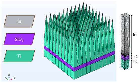
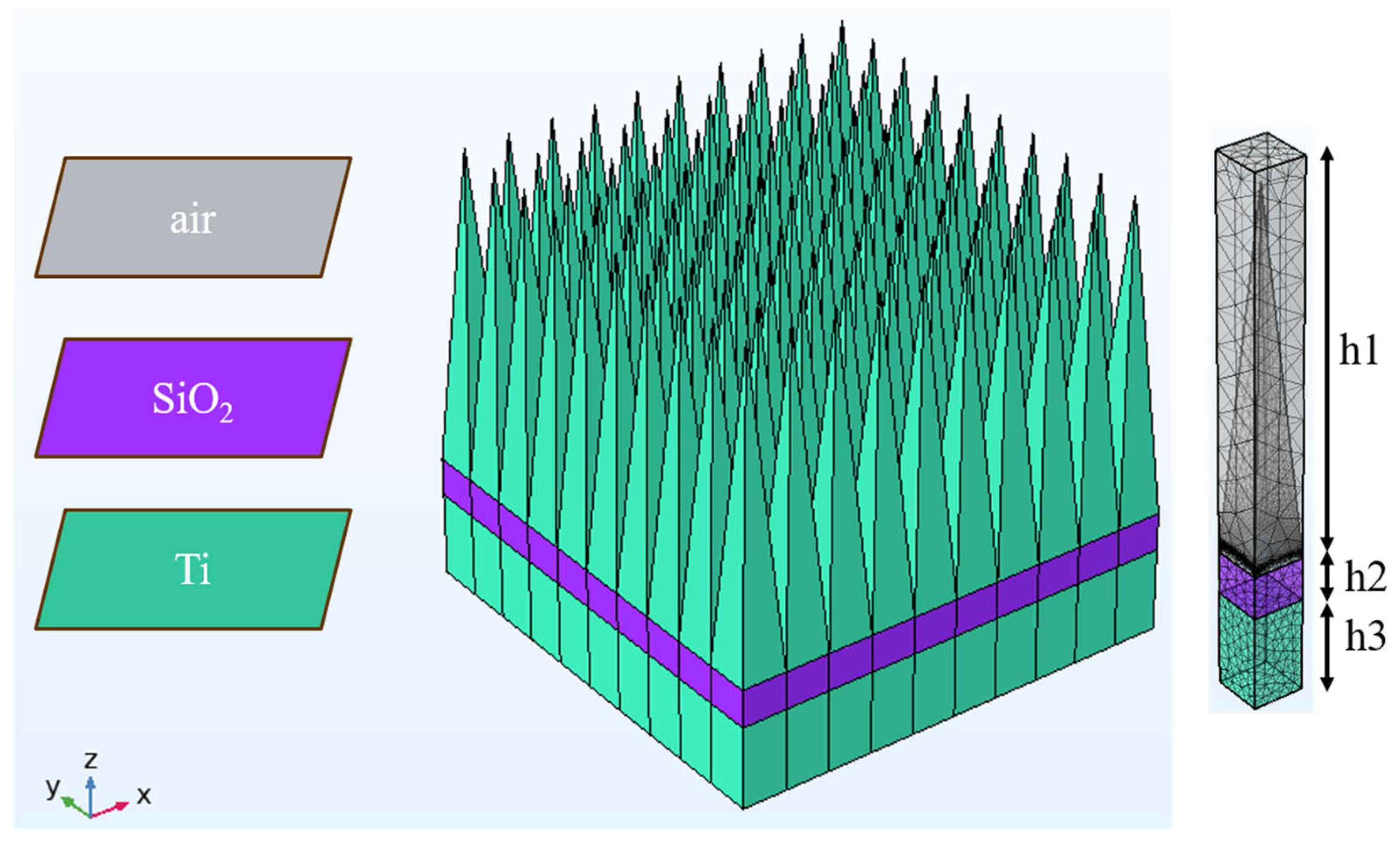
The proposed optical absorber structure is illustrated in Figure 1. The design comprises a three-layer configuration, consisting of a continuous Ti ground plane (h3), a SiO2 dielectric spacer (h2), and a top Ti tetrahedral nanostructure (h1). The absorber is constructed based on a periodic square unit cell, where the lateral dimension (p) is initially fixed at 100 nm for both the Ti ground layer and the SiO2 layer to ensure structural consistency. The thicknesses of the Ti ground layer (h3) and the SiO2 dielectric layer (h2) are set to 110 nm and 30 nm, respectively, while the height of the Ti tetrahedral structure (h1) is defined as 380 nm. These initial parameters are selected as a baseline configuration for subsequent optimization. To systematically evaluate the optical performance, a comprehensive parametric study is conducted over a broad wavelength range from 200 nm to 3000 nm, covering the ultraviolet, visible, and near-infrared regions. The geometric parameter p is varied from 60 nm to 140 nm with an increment of 10 nm to investigate its influence on the effective refractive index profile and light coupling behavior. The thickness of the Ti ground layer (h3) is swept from 70 nm to 150 nm with a step size of 10 nm to ensure sufficient suppression of transmission, while the SiO2 layer thickness (h2) is varied from 10 nm to 50 nm with a step size of 5 nm to analyze its role in optical cavity effects and phase modulation. In addition, the height of the Ti tetrahedral structure (h1) is adjusted from 340 nm to 420 nm with an increment of 10 nm to explore its impact on light confinement and plasmonic resonance enhancement.
Figure 1.
Structure of the investigated absorber.
The proposed Ti tetrahedral nanostructure is considered experimentally feasible using current semiconductor nanofabrication technologies. In practical fabrication, nanoscale periodic patterns can be defined using electron-beam lithography, nanoimprint lithography, or focused ion beam patterning, followed by reactive ion etching or inductively coupled plasma etching to form tapered sidewalls and sharp apex geometries. The proposed structure mainly relies on controllable anisotropic etching and therefore remains compatible with existing semiconductor micro/nanofabrication processes. In practical fabrication, the sidewall angle and apex sharpness of the tetrahedral structure can be controlled through anisotropic etching parameters, including etching power, gas composition, chamber pressure, and etching duration during RIE or ICP processing. In addition, because the proposed absorber employs a relatively simple periodic geometry rather than highly complex multilayer resonator arrays, good large-area uniformity and structural reproducibility are considered achievable using current semiconductor nanofabrication technologies. Minor fabrication deviations in sidewall angle or apex geometry may slightly influence the local field distribution; however, the broadband absorption behavior is expected to remain relatively stable because the proposed mechanism mainly relies on distributed impedance matching and broadband plasmonic confinement rather than a single narrowband resonance mode. These parameter ranges are carefully selected to balance computational efficiency, fabrication feasibility, and performance optimization, enabling identification of the optimal structural configuration. The numerical simulations are performed using COMSOL Multiphysics (version 6.0). A finite element method (FEM) is employed to solve the electromagnetic field distributions within the computational domain.
In this study, the wavelength-dependent complex refractive index (n + ikn) and corresponding optical constants of Ti, SiO2, and other investigated materials were obtained from the built-in optical material database provided in COMSOL Multiphysics. Because Ti is a dispersive metallic material, its refractive index and extinction coefficient are not fixed constants but vary with wavelength across the ultraviolet, visible, and near-infrared spectral regions. Among the investigated materials, Ti exhibits a relatively large extinction coefficient (k) over a broad spectral range, indicating strong intrinsic optical loss and efficient electromagnetic energy dissipation capability. This optical characteristic plays an important role in suppressing reflection, enhancing plasmonic confinement, and achieving ultrabroadband near-perfect absorption behavior in the proposed absorber structure. The discretized model consists of 90,680 finite elements, including 90,645 tetrahedral elements, complemented by 19,368 triangular boundary elements, 676 edge elements, and 17 vertex elements, with a total of 17,638 mesh nodes, ensuring a high-resolution spatial representation of the structure. The mesh quality is carefully evaluated, with a minimum element quality of 0.04722 and an average quality of 0.6318, indicating a stable and reliable mesh for electromagnetic simulations. The element volume ratio is 8.618 × 10⁻⁷, demonstrating a well-controlled distribution of element sizes across the geometry, particularly in regions with sharp geometrical features and strong field gradients. The total mesh volume is calculated as 5.90 × 10⁶ nm3. These mesh characteristics confirm that the computational model is sufficiently refined to accurately capture localized electromagnetic field variations, especially in regions exhibiting strong plasmonic effects and multi-scale light confinement. Consequently, the numerical results provide a reliable basis for analyzing absorption mechanisms and optimizing broadband optical performance.
3. Results and Discussion
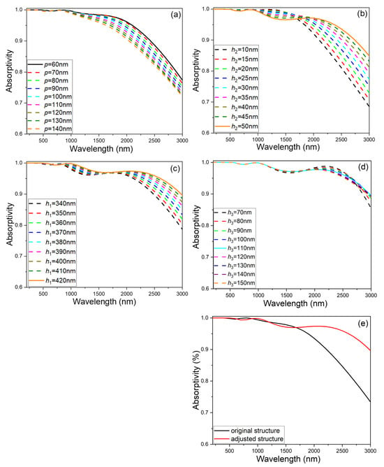
Figure 2a illustrates the influence of the square unit cell (p value) width on the absorption characteristics of the proposed optical absorber. As the unit cell width increases from 60 nm to 140 nm, a pronounced reduction in absorptivity is observed in the long-wavelength region (λ > ~1000 nm). Consequently, the effective absorption bandwidth (absorptivity > 0.9) decreases from 200 to 3000 nm to approximately 200–2450 nm. This result indicates that the lateral dimension of the unit cell is a key factor governing the ultrabroadband absorption behavior, particularly in the near-infrared regime. This behavior can be understood from the perspective of geometric scaling and its influence on the electromagnetic field distribution. Increasing the unit cell width enlarges the base dimension of the Ti tetrahedral structure and reduces the inclination angle of its sidewalls. Such geometric modification weakens the graded refractive index transition along the vertical direction, thereby degrading impedance matching between free space and the absorber.
Figure 2.
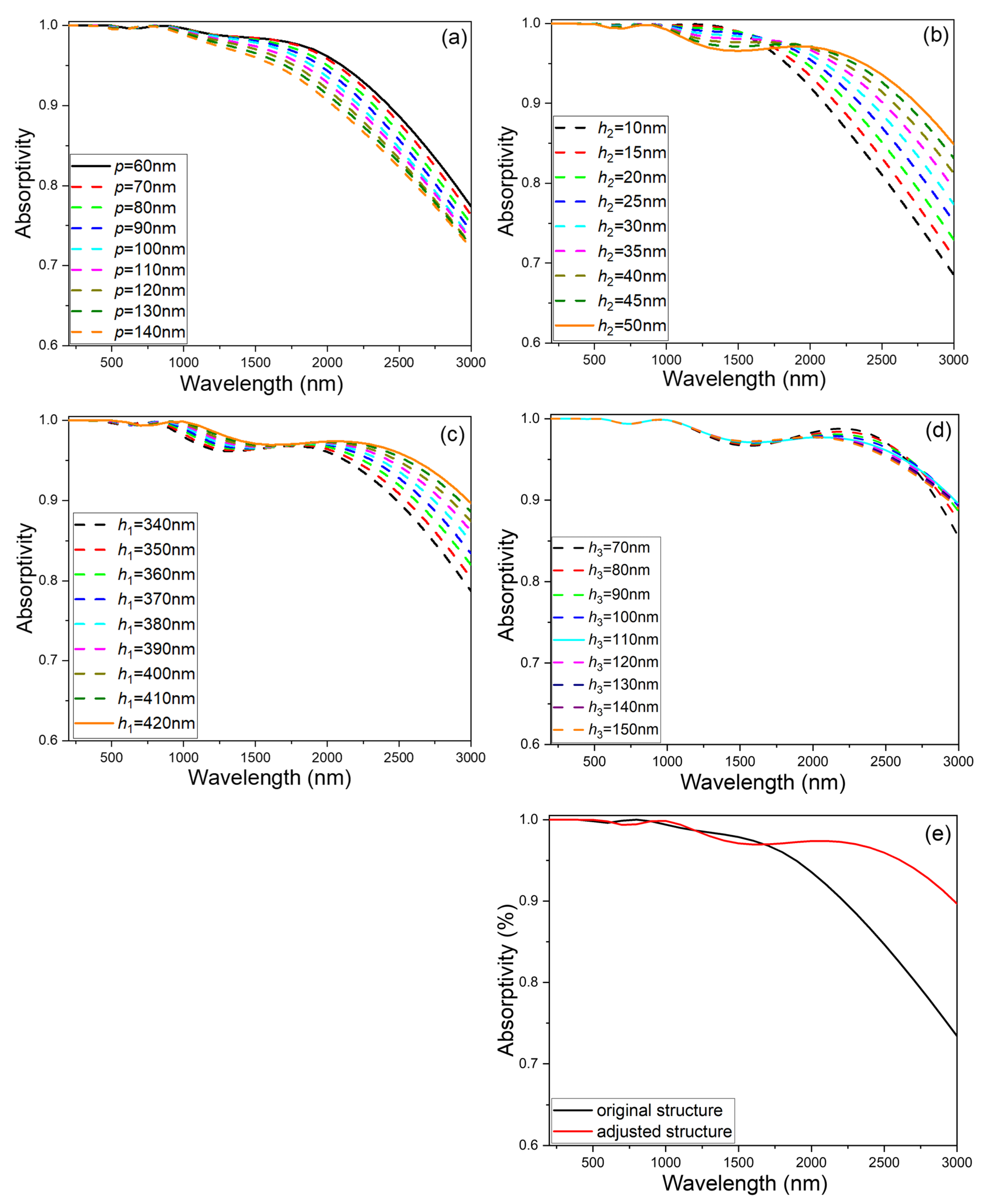
Effects of the different structure parameters on absorption characteristics of the investigated absorber (a) p value and the thicknesses of (b) h2, (c) h1, and (d) h3 layers. (e) Absorption characteristics of the designed absorber with original and modified parameters.
As a result, reflection losses increase at longer wavelengths, where efficient impedance matching is more critical for maintaining high absorptivity. The enlarged geometry reduces the degree of electromagnetic field confinement and weakens the excitation of LSPR at the metal–dielectric interface. Since broadband absorption relies on strong light–matter interaction and multi-mode coupling, the reduction in field localization directly limits absorption efficiency in the long-wavelength region. It should be noted that the unit cell width was not reduced below 60 nm because the optimized structure with p = 60 nm already achieves an ultrabroadband absorption range of 200–3000 nm, which is sufficient for practical applications. Further reduction in the unit cell width would increase fabrication difficulty and sensitivity to process variations. Therefore, a unit cell width of 60 nm provides a reasonable balance between optical performance and fabrication feasibility. The influence of the bottom Ti layer thickness (h3) was investigated. The results indicate that when the thickness of the h3 layer increases from 70 nm to 150 nm, the effective absorption bandwidth remains nearly unchanged, consistently spanning approximately 200–2400 nm.
This negligible variation suggests that the h3 layer does not play a dominant role in determining the spectral absorption characteristics of the structure. From a physical standpoint, the bottom Ti layer primarily functions as a reflective ground plane that suppresses transmission. Due to the inherently high optical loss and metallic nature of Ti, incident electromagnetic waves are largely reflected or dissipated before penetrating through the structure. In metallic absorbers, the penetration depth of incident electromagnetic waves is generally limited by the optical skin depth of the metal. When the Ti substrate thickness exceeds the corresponding skin depth, the transmitted electromagnetic waves decay exponentially inside the metallic layer and become nearly negligible. Under this condition, the absorber effectively satisfies the near-zero transmission requirement for near-perfect absorption. Therefore, further increasing the Ti substrate thickness mainly strengthens the reflective backplane effect rather than substantially modifying the absorption spectrum. As long as the Ti layer is sufficiently thick to prevent transmission (i.e., beyond the skin depth), further increases in thickness do not significantly influence the absorption behavior. Therefore, the absorption performance is mainly governed by the upper Ti tetrahedral structure and the intermediate SiO2 layer, which are responsible for impedance matching and plasmonic resonance effects. The h3 layer mainly ensures zero transmission, allowing the absorber to operate under the condition A ≈ 1 − R, where minimizing reflection becomes the key factor for achieving high absorptivity.
The influence of the SiO2 spacer thickness (h2) on the absorption behavior was systematically examined, and the results are shown in Figure 2b. As h2 increases from 10 nm to 50 nm, a wavelength-dependent response is observed. In the intermediate range (1000–1800 nm), the absorptivity decreases with increasing h2. In contrast, for wavelengths beyond 1800 nm, the absorptivity improves as h2 increases, accompanied by a clear redshift in the long-wavelength absorption edge from approximately 2100 nm to 2700 nm. This behavior arises from the dual role of the dielectric spacer in phase modulation and field coupling. Increasing h2 effectively enlarges the optical path length and modifies the phase accumulation within the structure, which promotes constructive interference and enhances absorption at longer wavelengths. This also facilitates a shift of the resonance condition toward the infrared region. However, in the shorter and intermediate wavelength ranges, a thicker dielectric layer reduces the coupling efficiency between the incident electromagnetic waves and the plasmonic modes supported by the metallic nanostructure, leading to reduced absorptivity. In addition, excessive SiO2 thickness introduces a stronger impedance mismatch and acts as a partial optical barrier, limiting electromagnetic field penetration into the lossy metallic region and increasing reflection losses. Therefore, an h2 thickness of 50 nm is selected as an optimal compromise, enabling enhanced long-wavelength absorption while avoiding excessive reflection and maintaining overall broadband performance.
Finally, the influence of the top Ti tetrahedral height (h1) on the absorption performance was systematically investigated, and the results are shown in Figure 2c. As h1 increases from 340 nm to 420 nm, the absorptivity is enhanced across nearly the entire wavelength range. In particular, a noticeable improvement is observed in the long-wavelength region, where the absorption edge exhibits a pronounced redshift from approximately 2400 nm to 3000 nm. These results indicate that the height of the tetrahedral structure is a key parameter governing both the absorption efficiency and the achievable spectral bandwidth. This behavior can be understood in terms of geometric modulation of the effective refractive index and electromagnetic field distribution. Increasing h1 results in a more elongated tetrahedral geometry, which creates a smoother and more gradual transition of the effective refractive index from free space to the metallic substrate.
The graded-index profile improves impedance matching and enhances the coupling of incident electromagnetic waves into the absorber, particularly at longer wavelengths. Increasing h1 also extends the optical interaction length, promoting multiple reflections, stronger electromagnetic field confinement, and enhanced LSPR excitation at the metal–dielectric interfaces. In addition, the elongated geometry supports broader resonant coupling and more efficient energy dissipation in the near-infrared region. Therefore, h1 = 420 nm is selected as the optimal parameter, enabling an effective absorption bandwidth (absorptivity > 0.9) spanning 200–3000 nm while maintaining structural simplicity and practical feasibility. As shown in Figure 2d, the optimized absorber exhibits three relatively weak absorption peaks located at approximately 600 nm, 1000 nm, and 2200 nm. These characteristic wavelengths are selected to further analyze the spatial distributions of the electric and magnetic field intensities, providing insight into the underlying absorption mechanisms.
The presence of multiple absorption peaks indicates that the broadband response originates from the superposition of several resonant modes rather than a single dominant resonance. At shorter wavelengths (around 600 nm), absorption is mainly associated with LSPR occurring near the apex and edges of the Ti tetrahedral structure, where strong electric field enhancement is observed. At intermediate wavelengths (around 1000 nm), the field distribution suggests a combination of plasmonic resonance and cavity-like effects within the SiO2 layer, leading to enhanced light confinement. At longer wavelengths (around 2200 nm), the absorption is primarily governed by extended electromagnetic field penetration and multi-scale resonance coupling, which contribute to the broadband behavior. Finally, we analyzed the influence of the h3 thickness variation on the absorption characteristics of our designed absorber. As shown in Figure 2d, within the wavelength range from 200 nm to approximately 1600 nm, the absorber with an h3 thickness of 110 nm achieves the highest absorptivity. Although this thickness does not yield the highest absorptivity in the 1600 nm to 2700 nm range, it is evident that the absorber exhibits the maximum absorption bandwidth when h3 is set to 110 nm. Figure 2e shows that the absorption intensity gradually decreases from the top tetrahedral structure toward the bottom metallic layer. This behavior indicates that most incident electromagnetic energy is mainly confined and dissipated in the upper nanostructured region, while the bottom Ti layer primarily acts as a reflective backplane to suppress transmission. These results confirm the effectiveness of the proposed structure for broadband light confinement and absorption. The proposed absorber maintained an absorptivity higher than 0.990 over the wavelength range of 200–1150 nm, while the average absorptivity across the entire 200–3000 nm spectral range reached 0.974, demonstrating excellent ultrabroadband absorption performance.
To further evaluate the impedance-matching characteristics of the proposed absorber, the effective optical impedance was calculated from the equivalent electromagnetic parameters of the structure. The normalized optical impedance could be retrieved from the simulated scattering parameters. The impedance can be calculated as:
where S11 and S21 are the reflection and transmission coefficients, respectively. For a reciprocal and symmetric structure, S11 = S22 and S21 = S12, and therefore the impedance retrieval can be performed using the simulated S11 and S21 parameters. The appropriate sign of the square root was selected to satisfy the passive-medium condition of Re(z) > 0. When the real part of the normalized impedance approaches unity and the imaginary part approaches zero, the impedance mismatch between the absorber and free space is minimized, thereby suppressing reflection and enhancing electromagnetic energy absorption. In this study, the wavelength-dependent permittivity and permeability values of the different materials were obtained from the built-in optical material database provided in COMSOL Multiphysics. Therefore, the calculated impedance behavior directly reflects the intrinsic optical properties and electromagnetic response of the investigated absorber structure.
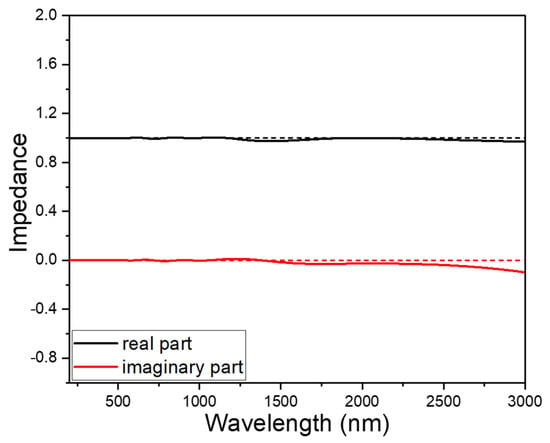
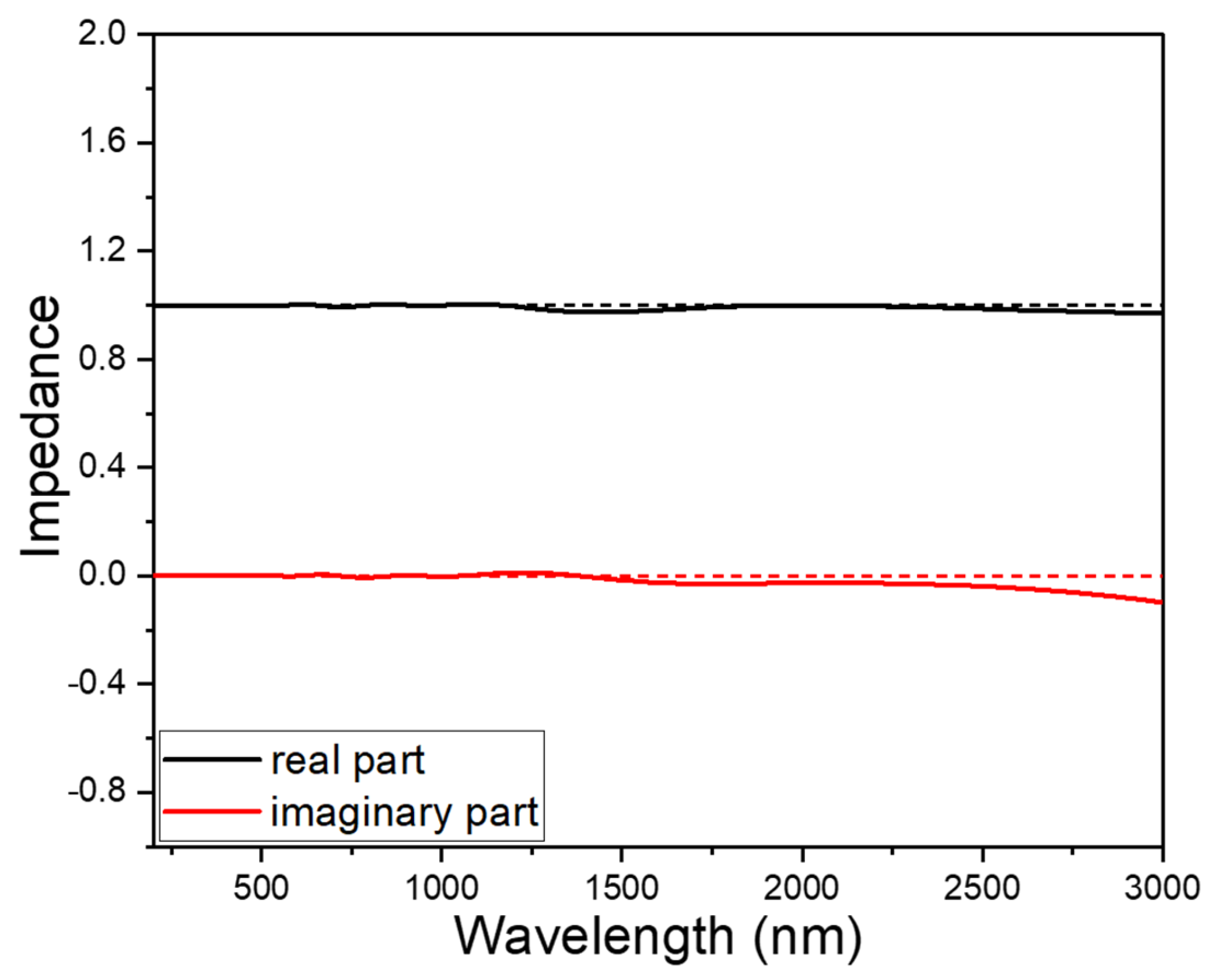
The variation in optical impedance with wavelength is presented in Figure 3. It is observed that the real part of the normalized impedance remains close to unity over a broad spectral range from 200 nm to 3000 nm. Meanwhile, the imaginary part is approximately zero within the wavelength range of 200–2500 nm. However, beyond 2500 nm, the imaginary component gradually deviates to slightly negative values, with the deviation becoming more pronounced as the wavelength increases. These results indicate that the proposed structure achieves near-ideal impedance matching with free space across most of the operating spectrum. When the real part of the impedance approaches unity and the imaginary part approaches zero, reflection at the air–absorber interface is effectively minimized, allowing incident electromagnetic waves to be efficiently coupled into the structure and subsequently dissipated. This condition directly corresponds to the high absorptivity observed across the ultraviolet-to-near-infrared spectral region. At longer wavelengths, impedance mismatch increases, leading to higher reflection and reduced absorption. The impedance analysis indicates that the broadband absorption performance is mainly governed by effective impedance matching.
Figure 3.
Optical impedance of the investigated absorber.
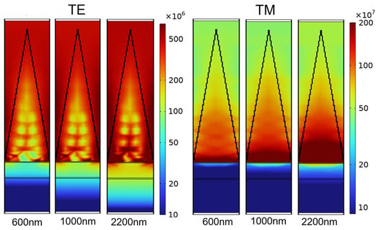
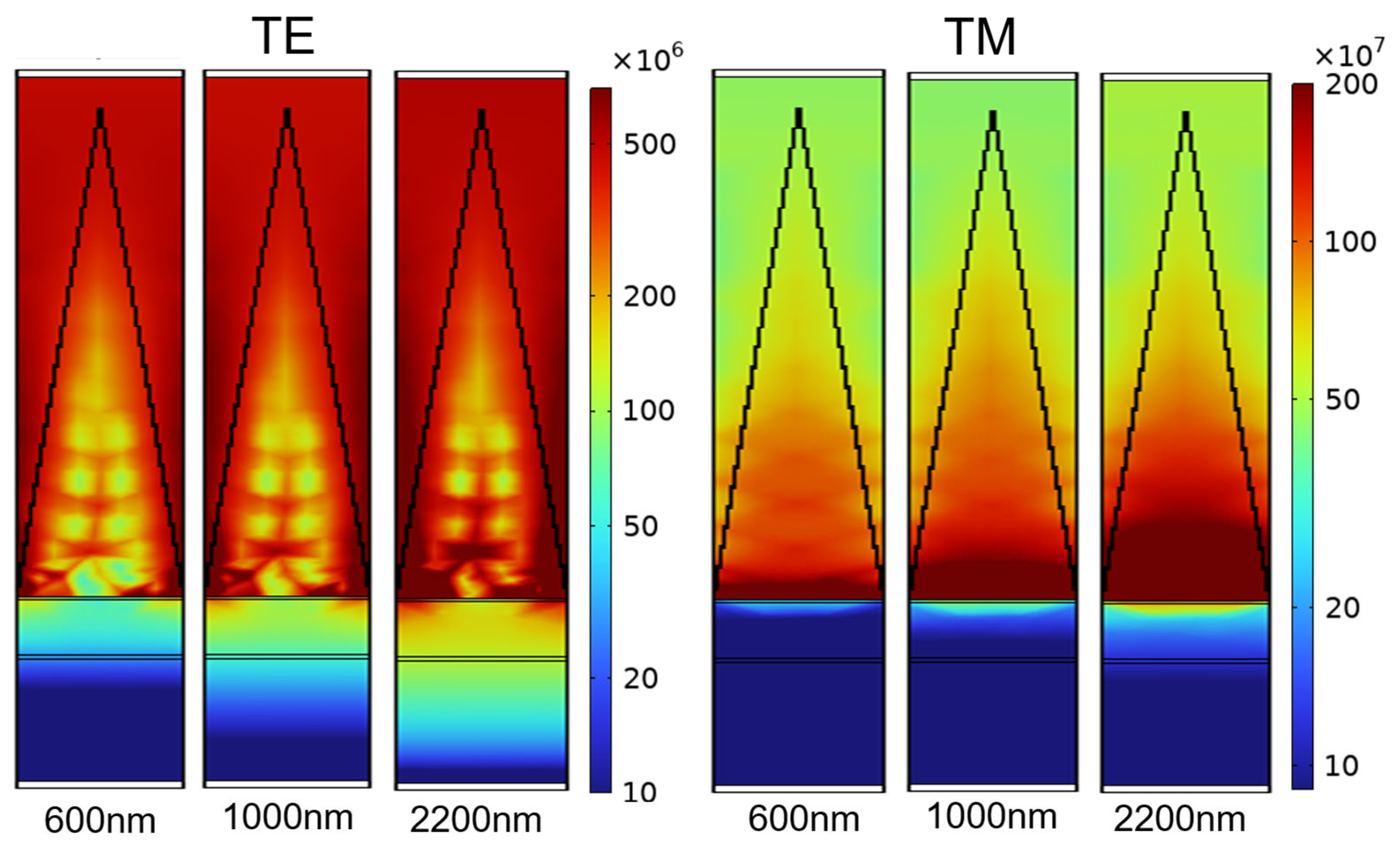
As shown in Figure 2d, the optimized absorber exhibits three relatively weak absorption peaks located at approximately 600 nm, 1000 nm, and 2200 nm. These representative wavelengths are selected to further examine the spatial distributions of the electric and magnetic field intensities, in order to elucidate the underlying absorption mechanisms. Figure 4 clearly demonstrates that the absorption intensity decays progressively from the top tetrahedral structure toward the bottom metallic layer. This top-to-bottom attenuation behavior provides important insight into the energy dissipation process within the absorber. Specifically, the incident electromagnetic waves are first strongly coupled into the apex and sidewall regions of the Ti tetrahedron, where localized field enhancement occurs. This indicates that the upper nanostructured region serves as the primary site for light trapping and energy absorption. As the electromagnetic waves propagate downward, their intensity gradually decreases due to continuous energy dissipation within the lossy metallic structure. The SiO2 layer further modulates the field distribution by introducing phase delay and enhancing confinement, while the bottom Ti layer acts as a reflective backplane that suppresses transmission and redirects residual energy back into the structure. This repeated interaction enhances absorption efficiency. Such a vertically decaying field distribution is characteristic of absorbers dominated by impedance matching and plasmonic confinement rather than purely resonant cavity modes.
Figure 4.
Electric and magnetic field intensity distributions at different wavelengths.
The result confirms that the proposed design effectively concentrates and dissipates electromagnetic energy in the upper region, thereby enabling efficient ultrabroadband absorption. The revised field distributions further reveal distinct wavelength- and polarization-dependent electromagnetic coupling characteristics. Under TE polarization, the regions exhibiting relatively strong absorption intensity gradually extend deeper into the lower Ti region as the wavelength increases from 600 nm to 2200 nm. In addition, several relatively low-field regions can be observed within the middle region of the tetrahedral structure, and the size of these low-field regions gradually decreases with increasing wavelength. This behavior indicates wavelength-dependent redistribution of electromagnetic energy and suggests the existence of multiple coupled resonant pathways within the absorber structure. In contrast, under TM polarization, the strongest field localization is mainly concentrated near the bottom region of the tetrahedral structure and the upper metal–dielectric interface. Furthermore, the field intensity in these highly confined regions becomes more pronounced as the wavelength increases, particularly at 2200 nm. These polarization-dependent field distributions confirm that the ultrabroadband absorption behavior originates from the synergistic interaction of impedance matching, plasmonic confinement, and distributed multi-mode electromagnetic coupling rather than from a single slow-light resonance mechanism. The strong field localization observed near the apex, sidewalls, and metal–dielectric interfaces is characteristic of localized surface plasmon resonance excitation, which enhances light–matter interaction and promotes electromagnetic energy dissipation within the lossy Ti structure. In addition, the gradual penetration of electromagnetic fields into the absorber with limited reflected-field concentration indicates improved impedance matching between free space and the absorber structure over a broad wavelength range.
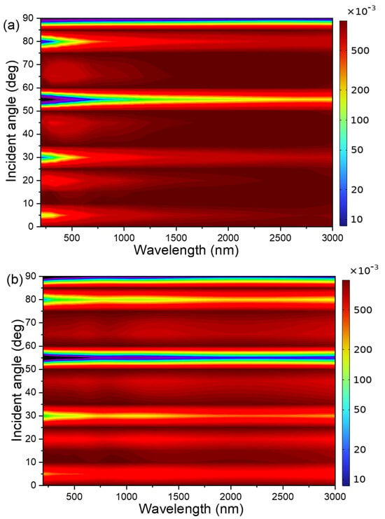
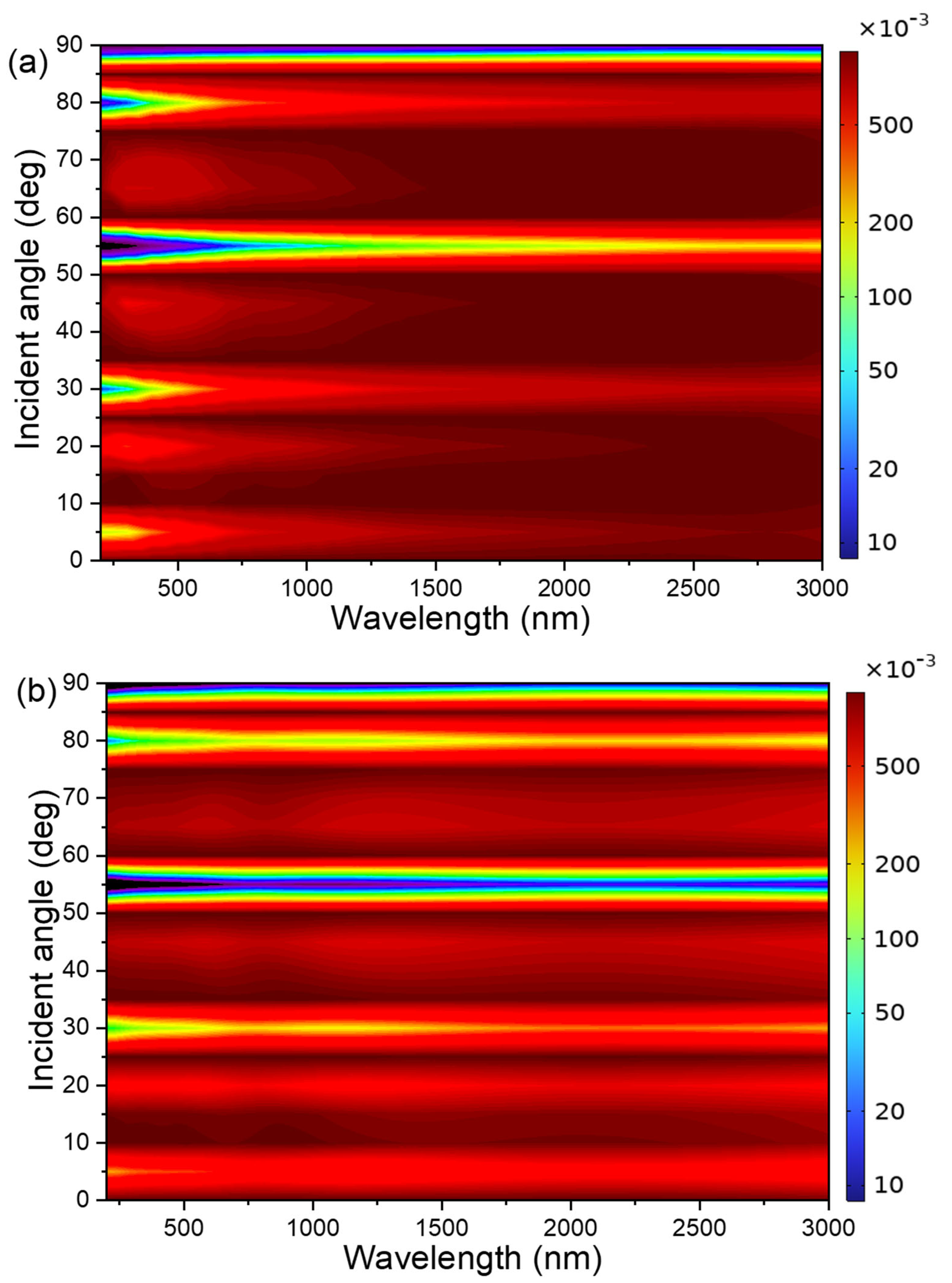
The angular dependence of the absorption performance for the proposed near-perfect ultra-wideband optical absorber was evaluated over incident angles ranging from 0° to 90° under both TE and TM polarizations, as shown in Figure 5a,b. As illustrated in Figure 5a, under TE polarization, the absorber exhibits noticeable reductions in absorptivity at incident angles around 5°, 30°, 55°, and 80°. Among these, the most pronounced degradation occurs near 55°, where the low-absorptivity region extends across nearly the entire spectral range from 200 nm to 3000 nm. At other incident angles, the reduction in absorptivity is primarily confined to the short-wavelength region, while relatively high absorption is maintained over the remaining spectrum. Furthermore, when the incident angle approaches 90°, the absorption intensity decreases significantly because the electromagnetic wave propagates nearly parallel to the absorber surface, resulting in weaker electromagnetic field coupling and increased reflection. In contrast, as shown in Figure 5b, the effect becomes more significant under TM polarization. Similarly, under TM polarization, the absorptivity also decreases markedly as the incident angle approaches 90°, further confirming the deterioration of impedance matching and the reduced effectiveness of plasmonic resonance excitation at grazing incidence.
Figure 5.
Angular absorption distributions under (a) TE and (b) TM polarizations at different wavelengths.
The absorber exhibits more pronounced and broader low-absorptivity regions at incident angles around 5°, 30°, 55°, and 80°. In particular, at 30°, 55°, and 80°, the degradation in absorption extends over almost the entire wavelength range (200–3000 nm), indicating a stronger sensitivity to incident angle under TM polarization. This polarization- and angle-dependent behavior can be attributed to variations in electromagnetic field coupling and impedance matching conditions. Under TE polarization, the electric field remains parallel to the surface, which allows relatively stable excitation of surface modes over a range of incident angles. However, at specific angles, phase mismatch and reduced coupling efficiency lead to decreased absorption. Under TM polarization, the electric field includes a normal component relative to the surface, making the excitation of plasmonic and cavity modes more sensitive to angular variation. As the incident angle increases, the effective impedance mismatch becomes more pronounced, leading to increased reflection and reduced absorption. These results suggest that while the proposed absorber performs well under normal incidence, its angular stability is limited and strongly polarization-dependent.
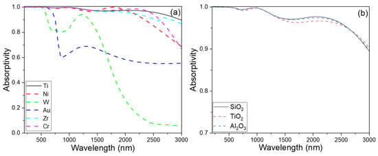
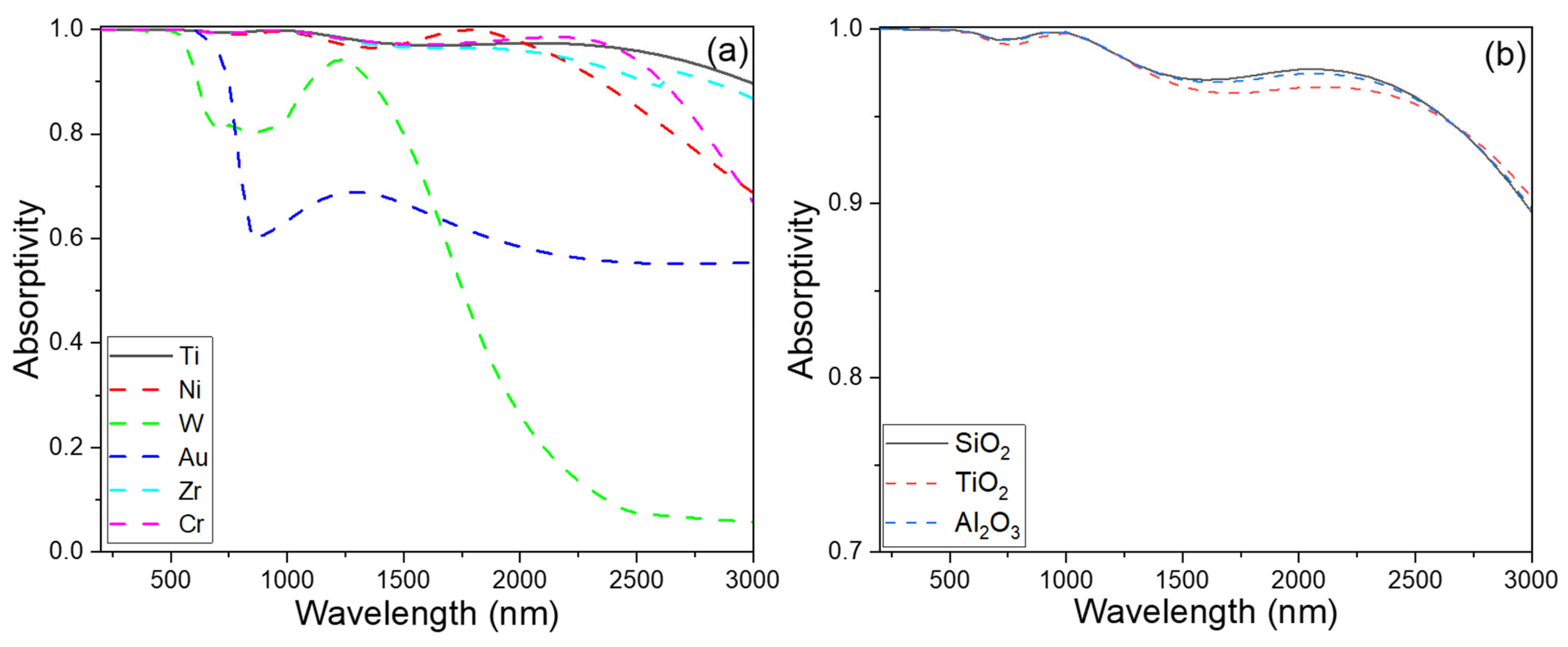
Figure 6 compares the absorption performance of the proposed absorber when different metals are employed for the tetrahedral top structure, including Ti, Ni, W, Au, Zr, and Cr. It is observed that all investigated metals exhibit near-perfect absorption behavior in the short-wavelength region (λ < 700 nm), indicating that strong intrinsic material loss and efficient excitation of surface plasmonic modes dominate the absorption mechanism in this spectral range. Among the considered materials, Zr demonstrates absorption characteristics most comparable to those of Ti. However, both the overall absorptivity and the effective absorption bandwidth achieved with Zr remain inferior to those obtained using Ti. For the other metals, either the absorptivity is significantly reduced or the absorption bandwidth is substantially narrower. For example, W and Au exhibit near-perfect absorption only within relatively limited spectral ranges of approximately 200–600 nm and 200–700 nm, respectively. The near-perfect absorption behavior of the proposed structure originates from the combined effects of impedance matching, LSPR, and the graded refractive-index transition induced by the tetrahedral geometry. The tapered structure reduces reflection and enhances electromagnetic-wave coupling into the absorber, while strong field localization near the apex and sidewalls promotes efficient energy dissipation within the lossy metallic structure. In addition, the bottom Ti layer acts as a reflective backplane that suppresses transmission, enabling near-perfect absorption with minimized reflection and negligible transmission. The absorption performance also depends on the optical properties of the metals, particularly their intrinsic loss and impedance-matching capability. Ti exhibits relatively high optical loss over a broad spectral range, providing efficient electromagnetic energy dissipation and broadband absorption.
Figure 6.
Effects of the (a) different metals and (b) different oxides on absorption characteristics of the investigated absorber.
In contrast, Au exhibits lower intrinsic loss, resulting in narrower absorption bandwidths, while excessive damping in W and Cr weakens plasmonic confinement and reduces absorption efficiency. Therefore, Ti provides the most favorable balance between optical loss, plasmonic confinement, and impedance matching, resulting in superior ultrabroadband near-perfect absorption performance. Figure 6b has been further revised to include comparisons using TiO2 and Al2O3 dielectric layers in place of SiO2. The results indicate that the absorption bandwidths of the three oxide materials are relatively similar. However, the structure employing TiO2 exhibits slightly lower absorptivity and average absorption performance compared with those using SiO2 and Al2O3. The average absorptivities of the structures incorporating SiO2, TiO2, and Al2O3 are 0.974, 0.971, and 0.973, respectively. This result suggests that although the dielectric oxide layer has some influence on impedance matching and electromagnetic field confinement, the overall ultra-wideband absorption performance remains relatively stable for different oxide materials. The slightly reduced performance observed for TiO2 may be associated with its relatively high refractive index, which alters the impedance matching condition and weakens efficient electromagnetic energy coupling within the absorber structure.
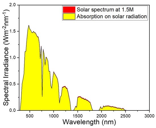
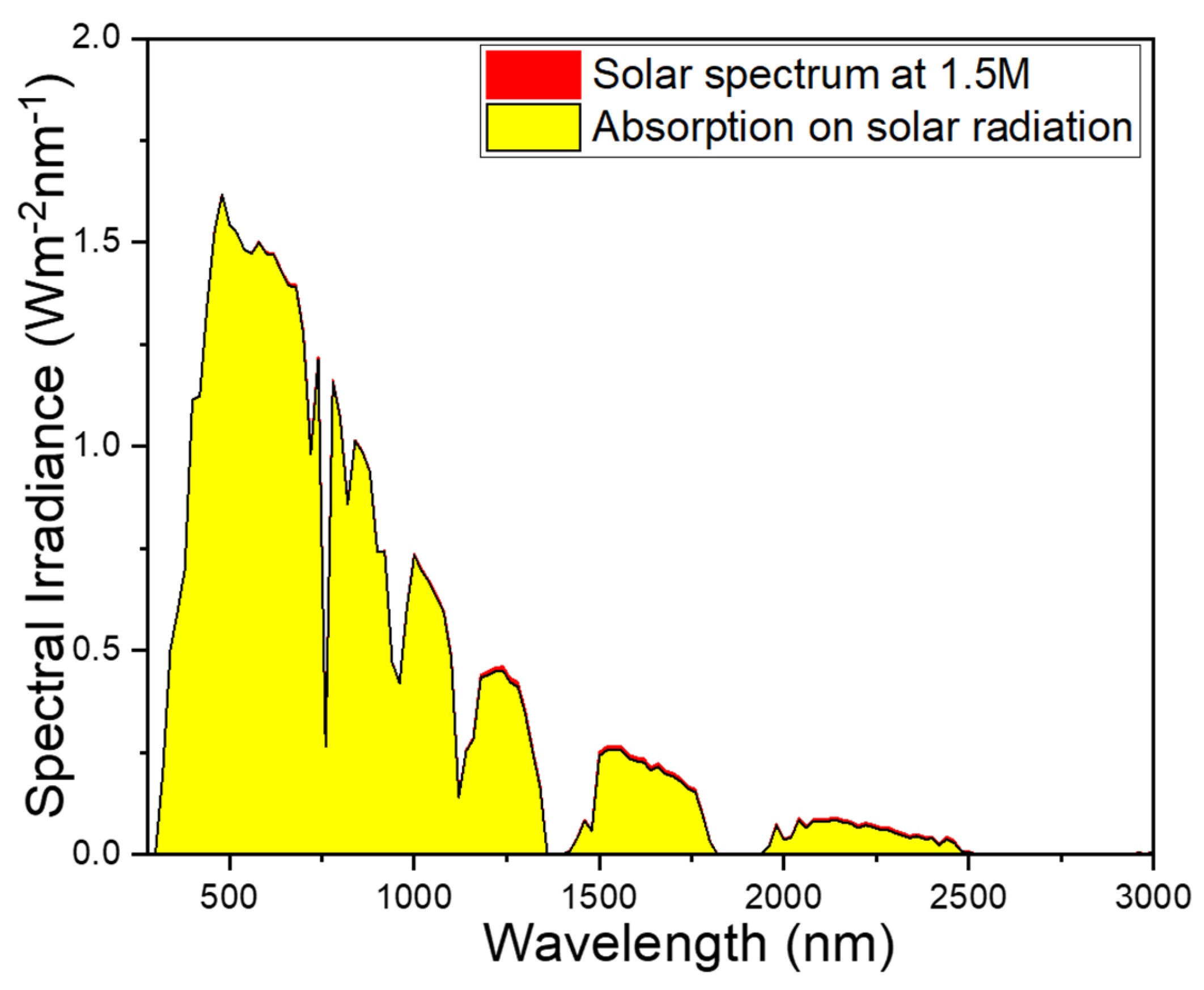
Figure 7 presents the simulated solar absorption performance of the proposed absorber under the AM1.5 illumination condition. The calculated average absorptivities within the wavelength ranges of 280–400 nm, 400–700 nm, 700–1400 nm, and 1400–3000 nm are 0.9997, 0.9985, 0.9913, and 0.9640, respectively. The overall average absorptivity across the entire solar spectral range from 280 to 3000 nm reaches 0.9886, demonstrating excellent ultrabroadband solar absorption capability. Furthermore, throughout the entire wavelength range from 280 to 3000 nm, the absorptivity remains consistently high over most wavelengths, indicating that the proposed structure can sustain efficient electromagnetic energy confinement and dissipation across an ultrabroadband spectral region. Because the absorptivity of the proposed absorber remains higher than 0.980 over most wavelengths below approximately 1300 nm, the absorbed solar irradiance almost completely overlaps with the AM1.5 solar spectrum in Figure 7. This behavior indicates extremely efficient optical energy dissipation rather than the absence of energy loss mechanisms. At longer wavelengths (>1300 nm), the absorptivity gradually decreases due to increasing impedance mismatch and weaker electromagnetic field confinement, leading to partial reflection losses and the appearance of unabsorbed solar irradiance. These results are consistent with the absorption and impedance characteristics presented in Figure 2 and Figure 3.
Figure 7.
Simulation absorption spectrum of the designed absorber.
These results demonstrate that the proposed optical absorber satisfies the essential characteristics of a near-perfect absorber, namely extremely low reflection, negligible transmission, and highly efficient optical energy dissipation within the structure. The high absorption efficiency of the proposed absorber originates from the combined effects of the Ti tetrahedral nanostructure, the SiO2 dielectric spacer, and the Ti reflective substrate. In the ultraviolet and visible regions (280–700 nm), absorption is mainly dominated by LSPR excited at the metal–dielectric interfaces and sharp tetrahedral features. The tapered geometry further enhances electromagnetic field localization and light trapping, promoting efficient energy dissipation within the lossy Ti structure. In the near-infrared region (700–3000 nm), broadband absorption is mainly governed by impedance matching and the graded refractive-index transition induced by the tapered geometry, which reduces reflection and improves electromagnetic-wave coupling into the absorber. Meanwhile, the bottom Ti layer suppresses optical transmission and enhances internal reflections, increasing the optical interaction length and energy dissipation efficiency. As a result, the proposed structure achieves stable ultrabroadband absorption across most of the AM1.5 solar spectrum while maintaining structural simplicity.
To further clarify the advantages of the proposed absorber, Table 1 compares the present Ti/SiO2/Ti tetrahedral absorber with several recently reported broadband or near-perfect optical absorbers. Although many reported absorbers exhibit high absorption efficiencies and broad spectral responses, they often rely on multilayer ring stacks, cascade optical cavities, graphene-assisted plasmonic coupling, or complex multi-resonator metamaterial patterns to achieve ultrabroadband absorption. Some structures also require advanced material systems such as TiN, Dirac semimetals, or multilayer metasurface architectures, which may increase fabrication complexity, material growth difficulty, and process sensitivity. In contrast, the proposed absorber consists of only three functional layers, namely a Ti reflective substrate, a SiO2 dielectric spacer, and a Ti tetrahedral nanostructure. Despite this structurally simple configuration, the proposed absorber achieves a near-unity absorptivity of 0.9999 at 200 nm, maintains an effective absorption bandwidth (A > 0.9) spanning 200–3000 nm, and exhibits a high average solar absorptivity of 0.9886 under AM1.5 illumination from 280 to 3000 nm. These results demonstrate that the proposed structure provides an excellent balance among structural simplicity, ultrabroadband near-perfect absorption performance, and high-efficiency solar-energy harvesting capability.
Table 1.
Comparison of the proposed absorber with representative broadband optical absorbers.
4. Conclusions
In this study, a structurally simple yet highly efficient ultrabroadband near-perfect optical absorber was successfully designed and analyzed based on a three-layer Ti/SiO2/Ti tetrahedral configuration. Through systematic parametric optimization, the proposed structure achieved an absorptivity of 0.9999 at 200 nm and maintained an effective absorption bandwidth (absorptivity > 0.9) spanning 200–3000 nm, covering the ultraviolet, visible, and near-infrared spectral regions. The results demonstrated that the unit cell width and tetrahedral height are the dominant parameters controlling broadband absorption behavior, while the Ti ground layer primarily functions as a transmission-blocking reflective substrate once its thickness exceeds the optical skin depth. Detailed electromagnetic analysis revealed that the ultrabroadband absorption originates from the synergistic interaction of impedance matching, localized surface plasmon resonance, graded refractive index transition, and multi-scale electromagnetic field confinement. The tapered tetrahedral geometry enables efficient coupling of incident electromagnetic waves into the absorber while suppressing reflection losses across a broad spectral range. Impedance retrieval further confirmed that the normalized impedance remains close to that of free space over most wavelengths, validating the near-perfect absorption behavior. In addition, field distribution analysis demonstrated that electromagnetic energy is predominantly confined and dissipated near the upper tetrahedral region and metal–dielectric interfaces. The AM1.5 simulation results showed an overall average absorptivity of 0.9886 from 280 to 3000 nm, confirming the excellent solar absorption capability of the proposed design. Owing to its combination of structural simplicity, fabrication feasibility, and ultrabroadband optical performance, the proposed absorber provides a feasible design strategy for next-generation ultrabroadband optical absorbers.
Author Contributions
Conceptualization, Y.D., W.-M.C. and C.-F.Y.; methodology, Y.D., Y.-J.L., W.-M.C. and C.-F.Y.; validation, Y.D., Y.-J.L., W.-M.C., Y.-C.T. and C.-F.Y.; formal analysis, Y.D., Y.-J.L., W.-M.C., Y.-C.T. and C.-F.Y.; investigation, Y.D., W.-M.C. and C.-F.Y.; data curation, Y.D., Y.-J.L., W.-M.C., Y.-C.T. and C.-F.Y.; writing—original draft preparation, Y.D., W.-M.C. and C.-F.Y.; writing—review and editing, Y.D., W.-M.C. and C.-F.Y.; visualization, Y.D., Y.-J.L., W.-M.C., Y.-C.T. and C.-F.Y. All authors have read and agreed to the published version of the manuscript.
Funding
This work is supported by the Guangdong Provincial Department of Science and Technology under Grant No. 2024A0505050048. This work was also supported by Summit-Tech Resource Corp., and by projects under Nos. NSTC 113-2221-E-390-011 and NSTC 114-2622-E-390-001.
Institutional Review Board Statement
Not applicable.
Informed Consent Statement
Informed consent was obtained from all subjects involved in the study.
Data Availability Statement
The data supporting the findings of this study are available from the corresponding authors upon reasonable request.
Conflicts of Interest
The authors declare no conflicts of interest.
References
- Landy, N.I.; Sajuyigbe, S.; Mock, J.J.; Smith, D.R.; Padilla, W.J. Perfect metamaterial absorber. Phys. Rev. Lett. 2008, 100, 207402. [Google Scholar] [CrossRef] [Scilit]
- Watts, C.M.; Liu, X.; Padilla, W.J. Metamaterial electromagnetic wave absorbers. Adv. Mater. 2012, 24, OP98–OP120. [Google Scholar] [CrossRef] [Scilit]
- Aydin, K.; Ferry, V.E.; Briggs, R.M.; Atwater, H.A. Broadband polarization-independent resonant light absorption. Nat. Commun. 2011, 2, 517. [Google Scholar] [CrossRef] [Scilit]
- Cui, Y.; Fung, K.H.; Xu, J.; Jin, Y.; He, S.; Fang, N.X. Ultrabroadband light absorption. Nano Lett. 2012, 12, 1443–1447. [Google Scholar] [CrossRef] [Scilit] [PubMed]
- Kats, M.A.; Blanchard, R.; Zhang, S.; Genevet, P.; Ko, C.; Ramanathan, S.; Capasso, F. Vanadium Dioxide as a Natural Disordered Metamaterial: Perfect Thermal Emission and Large Broadband Negative Differential Thermal Emittance. Phys. Rev. X 2013, 3, 041004. [Google Scholar] [CrossRef] [Scilit]
- Li, W.; Valentine, J. Metamaterial absorber photodetection. Nano Lett. 2014, 14, 3510–3514. [Google Scholar] [CrossRef] [Scilit] [PubMed]
- Zhu, B.; Zhao, Y.; Feng, Y. Ultrathin metamaterial absorber. Appl. Phys. Lett. 2010, 97, 051906. [Google Scholar] [CrossRef] [Scilit]
- Grant, J.; Ma, Y.; Saha, S.; Khalid, A.; Cumming, D.R.S. Metamaterial absorber. Opt. Lett. 2011, 36, 3476–3478. [Google Scholar] [CrossRef] [Scilit]
- Liu, X.; Tyler, T.; Starr, T.; Starr, A.F.; Jokerst, N.M.; Padilla, W.J. Infrared metamaterials. Phys. Rev. Lett. 2011, 107, 045901. [Google Scholar] [CrossRef] [Scilit]
- Cheng, Y.; Gong, R.; Cheng, Z. Design, fabrication and measurement of a broadband polarization-insensitive metamaterial absorber based on lumped elements. J. Appl. Phys. 2012, 111, 044902. [Google Scholar] [CrossRef] [Scilit]
- Hu, Y.; Chen, Z.; Yi, Z.; Cheng, S.; Ahmad, S.; Li, B. Ultra wideband solar energy absorption device based on multi-layered Ti-InAs cylinder metasurface. Phys. E 2026, 180, 116514. [Google Scholar] [CrossRef] [Scilit]
- Yang, X.; Guo, Y.; Cheng, S. Ultrabroadband absorber based on titanium nitride concentric dual-ring array for high-efficiency solar energy harvesting. Phys. B 2026, 733, 418581. [Google Scholar] [CrossRef] [Scilit]
- Fu, S.; Yang, X. A terahertz four-band high-sensitivity perfect absorber based on Dirac semimetal. Phys. Lett. A 2026, 587, 131760. [Google Scholar] [CrossRef] [Scilit]
- Qing, G.; Huang, J.; Zhang, D.; Zhai, X.; Liu, G.; Xia, S.-X. All-order dark mode plasmon-induced transparency underpinned by transitional resonance phase. Phys. Rev. B 2026, 113, 125413. [Google Scholar] [CrossRef] [Scilit]
- Gu, X.; Liu, X.; Yan, X.-F.; Du, W.-J.; Lin, Q.; Wang, L.-L.; Liu, G.-D. Polaritonic coherent perfect absorption based on self-hybridization of a quasi-bound state in the continuum and exciton. Opt. Express 2023, 31, 4691–4700. [Google Scholar] [CrossRef] [Scilit]
- Liu, J.-Q.; Zhou, Y.-X.; Li, L.; Wang, P.; Zayats, A.V. Controlling plasmon-induced transparency of graphene metamolecules with external magnetic field. Opt. Express 2015, 23, 12524–12532. [Google Scholar] [CrossRef] [Scilit] [PubMed]
- Huang, J.; Qing, G.; Zhang, D.; Zhai, X.; Peng, J.; Xia, S. Dynamically tunable and ultrastable plasmonic bound states in the continuum in bilayer graphene metagratings. Phys. Rev. B 2025, 112, 205421. [Google Scholar] [CrossRef] [Scilit]
- Li, X.; Zhang, Z.; Feng, H.; Zhou, Y.; Sun, P.; Nie, S.; Gao, Y. Ultra-broadband solar energy absorber based on Ti and TiN from visible to mid-infrared. Phys. Scr. 2023, 98, 105526. [Google Scholar] [CrossRef] [Scilit]
- Yuan, H.; Yi, Y.; Song, Q.; Yi, Z.; Sun, T.; Tang, C.; Zeng, Q.; Cheng, S.; Wu, P. Ultra-broadband absorber and perfect thermal emitter for high-efficiency solar energy absorption and conversion. Renew. Energy 2024, 237, 121818. [Google Scholar] [CrossRef] [Scilit]
- Jiang, J.; Yi, Y.; Song, Q.; Yi, Z.; Ma, C.; Zeng, Q.; Sun, T.; Cheng, S.; Yi, Y.; Akhtar, M.N. Multi-layer nanoring array-based ultra-wideband solar absorber for photothermal conversion. Phys. E 2025, 165, 116123. [Google Scholar] [CrossRef] [Scilit]
- Hsu, W.-L.; Lin, X.-Y.; Ho, C.-M.; Yang, C.-F.; Lai, K.-K. Ultra-broadband solar absorber design covering UV to NIR range based on Cr–SiO2 metamaterial planar stacked structures. Photonics 2025, 12, 907. [Google Scholar] [CrossRef] [Scilit]
- Xu, W.; Peng, C.; Feng, J.; Xia, Y.; Zhang, X. Refractory broadband absorber from visible to near infrared region. Optoelectron. Lett. 2026, 22, 129–133. [Google Scholar] [CrossRef] [Scilit]
- Chen, H.T. Interference theory absorber. Opt. Express 2012, 20, 7165–7172. [Google Scholar] [CrossRef] [Scilit]
- Ding, F.; Dai, J.; Chen, Y.; Zhu, J.; Jin, Y.; Bozhevolnyi, S.I. Broadband absorbers. Sci. Rep. 2016, 6, 39445. [Google Scholar] [CrossRef] [Scilit] [PubMed]
- Li, Z.; Butun, S.; Aydin, K. Lithography-free absorbers. ACS Nano 2014, 8, 8242–8248. [Google Scholar] [CrossRef] [Scilit] [PubMed]
- He, X.; Zhang, Y.; Liu, J. Plasmonic absorber. Phys. Chem. Chem. Phys. 2025, 27, 3307. [Google Scholar] [CrossRef] [Scilit]
- Islam, M.A.; Hasan, M.; Ahmed, R. Ultrabroadband absorber. Opt. Contin. 2025, 4, 756. [Google Scholar] [CrossRef] [Scilit]
- Rakhshani, M.R.; Karimi, F.; Rashki, M. Metamaterial absorber using cascaded ring resonators and optimization through machine learning for sensing applications. Sci. Rep. 2025, 15, 39977. [Google Scholar] [CrossRef] [Scilit]
- Sun, Y.; Ren, Y.; Qu, D.; Li, C. Optimized broadband metamaterial absorber for solar photothermal conversion. Appl. Therm. Eng. 2025, 273, 126590. [Google Scholar] [CrossRef] [Scilit]
- Tekcan, B.; van Kasteren, B.; Grayli, S.V.; Shen, D.; Tam, M.C.; Ban, D.; Wasilewski, Z.; Tsen, A.W.; Reimer, M.E. Semiconductor nanowire metamaterial for broadband near-unity absorption. Sci. Rep. 2022, 10, 2200215. [Google Scholar] [CrossRef] [Scilit]
- Pan, Y.Z.; Li, Y.C.; Chen, F.; Cheng, S.B.; Yang, W.X.; Wang, B.Y.; Yi, Z.; Yao, D.Z. Ultra-broadband solar absorber based on TiN metamaterial from visible light to mid-infrared. J. Opt. Soc. Am. B 2023, 40, 3057–3064. [Google Scholar] [CrossRef] [Scilit]
- Wu, F.Y.; Shi, P.C.; Yi, Z.; Li, H.L.; Yi, Y.G. Ultra-broadband solar absorber and high-efficiency thermal emitter from UV to mid-infrared spectrum. Micromachines 2023, 14, 985. [Google Scholar] [CrossRef] [Scilit]
- Chen, P.; Yi, Y.; Song, Q.; Yi, Z.; Yi, Y.; Cheng, S.; Zhang, J.; Tang, C.; Sun, T.; Zeng, Q. Simulation and analysis of a near-perfect solar absorber based on SiO2-Ti cascade optical cavity. Photonics 2024, 11, 604. [Google Scholar] [CrossRef] [Scilit]

Disclaimer/Publisher’s Note: The statements, opinions and data contained in all publications are solely those of the individual author(s) and contributor(s) and not of MDPI and/or the editor(s). MDPI and/or the editor(s) disclaim responsibility for any injury to people or property resulting from any ideas, methods, instructions or products referred to in the content. |
© 2026 by the authors. Licensee MDPI, Basel, Switzerland. This article is an open access article distributed under the terms and conditions of the Creative Commons Attribution (CC BY) license.