


Abstract
CsPbI3 exhibits multiple crystal phases, and the kinetic barriers for phase transitions are relatively low, facilitating the formation of abundant interphase boundaries (IBs) during phase transitions. These IB structures significantly influence the optoelectronic performance of the material. In this work, based on three types of CsPbI3 IB structures, we systematically investigate the effects of pressure on the formation feasibility and optoelectronic properties of these IBs by calculating their formation energies, band alignments, optical absorption characteristics, and carrier effective masses. The results show that moderate pressure can increase the formation feasibility of certain IB structures and effectively modulate the band alignment at the CsPbI3 IBs, thereby enabling the switching of different optoelectronic functions within the same material. Meanwhile, the application of pressure can also improve optical absorption and the spectroscopic-limited maximum efficiency, and reduce carrier effective masses in some IB systems, which is beneficial for enhancing carrier transport capabilities. This study demonstrates that pressure serves as an effective means to regulate the IB structures and optoelectronic properties of CsPbI3, providing theoretical support for the design of multifunctional optoelectronic materials based on IB engineering and for expanding photovoltaic applications.
1. Introduction
All-inorganic halide perovskite CsPbI3 is considered an important candidate material for photovoltaics [1,2], photodetection [3,4,5], light-emitting diodes [6,7], and other emerging optoelectronic devices [8], owing to its suitable optical bandgap, high optical absorption coefficient, good carrier transport capability, and relatively excellent chemical stability. Beyond these conventional fields, perovskite materials have recently garnered intensive attention as novel nonlinear optical components, particularly as saturable absorbers for generating ultrafast laser pulses [9] in the near-infrared region, which has further stimulated the search for materials with tunable optoelectronic properties. CsPbI3 mainly exists in four crystalline phases, including the α cubic phase, β tetragonal phase, γ orthorhombic phase, and δ non-perovskite orthorhombic phase. Among these, the α, β, and γ phases possess similar and excellent optoelectronic properties and are often collectively referred to as the black phase, while the δ phase is the non-photoactive yellow phase. Moreover, the three optoelectronically superior phases are thermodynamically unstable and spontaneously transform into δ-CsPbI3 after being left at room temperature for a period of time [10,11].
CsPbI3 is a typical multiphase material, and interphase boundaries (IBs) are more likely to appear in materials with polymorphism and low phase transition barriers. At room temperature, metastable γ-CsPbI3 spontaneously transforms into the thermodynamically stable δ phase, and the phase transition process is kinetically facile. Furthermore, reported computational results indicate that the transformation of CsPbI3 from the perovskite phase to the non-perovskite phase is not a single-step process but rather requires a multi-step transition involving three intermediate states, accompanied by the gradual disruption of the corner-sharing connectivity of PbI6 octahedra and the formation of edge-sharing connectivity [12]. X-ray diffraction measurements have shown that synthesized CsPbI3 contains crystalline phases other than the perovskite and non-perovskite phases [13,14,15], indirectly confirming the existence of intermediate phases. Combining theoretical simulations and experimental results, it can be inferred that the phase transition of CsPbI3 readily involves the coexistence of multiple crystalline phases, including intermediate phases, accompanied by grain boundaries or IBs [16,17,18,19]. Grain boundaries and IBs in CsPbI3 polycrystalline films have a considerable impact on the optoelectronic performance of CsPbI3-based devices. For example, defects such as vacancies and dangling bonds may exist at grain boundaries, which can trap carriers and thus affect carrier transport, leading to degradation of optoelectronic performance [20]. Meanwhile, IB structures can cause relative shifts in the band edges on both sides of the interface, leading to different band alignment configurations, which, in turn, affect the separation, recombination, and directional transport of photogenerated carriers [16,21].
Currently, extensive research has been conducted on issues such as grain boundary defects, ion migration, non-radiative recombination, and grain orientation regulation in perovskite materials, leading to a relatively systematic and in-depth understanding [20,22,23,24,25]. In contrast, IBs arise directly from the structural transformation between different crystalline phases and better reflect the characteristics of multiphase coexistence and stepwise phase transitions in CsPbI3 [12,26,27,28]. However, because the phase transition of CsPbI3 usually involves complex lattice reconstruction, changes in the connectivity of PbI6 octahedra, and local structural distortions, experimentally capturing the coherent IB structures in real time at the atomic scale remains challenging. Although some relevant studies have been reported, key issues regarding how IB structures affect carrier transport and optoelectronic response still warrant further in-depth investigation.
Recently, Yin’s group explored the phase transition process at the atomic level. Based on the transformation from α/γ-CsPbI3 to δ-CsPbI3, they constructed various IB structures and revealed the regulatory effects of different phase compositions and ratios on IB stability, band alignment, and carrier lifetime [16]. Halide perovskites generally feature relatively soft lattices [29], and their PbI6 octahedral distortions, phase stability, and electronic structures are readily modulated by external stress or pressure. Reported studies have shown that pressure can effectively adjust the stability, bandgap, and optical absorption properties of halide perovskites such as CsPbI3 [30,31,32]. Moreover, compared with doping or compositional regulation, hydrostatic pressure does not alter the chemical composition of the material or introduce additional extrinsic impurities, making it a relatively clean means of property modulation [33]. Therefore, based on the previously constructed CsPbI3 IB structures [16], we further introduce hydrostatic pressure as a regulation parameter and systematically investigate its effects on formation feasibility, band alignment, and carrier properties of three CsPbI3 interphase boundaries (α-MS3, γ-MS1, and γ-MS2) using first-principles calculations.
Our results indicate that the responses of the α-MS3, γ-MS1, and γ-MS2 IBs to pressure differ significantly: the formation feasibility of γ-MS2 decreases with increasing pressure; the formation feasibility of γ-MS1 is less affected by pressure within the range of less than 3 GPa; and the formation feasibility of α-MS3 is enhanced in the range of 2-5 GPa, suggesting that moderate pressure is beneficial for its stable existence. Regarding the modulation of band alignments, α-MS3 maintains a Type-II within 0-4 GPa and transforms to Type-III at 5 GPa; γ-MS1 and γ-MS2 exhibit an evolution of Type-II → Type-I → Type-II. This modulation originates from the different pressure responses of the band edges in the different crystalline phases and the enhanced Pb-I orbital hybridization. In terms of optoelectronic performance, for Type-II CsPbI3 IBs, moderate pressure reduces the bandgap, thereby enhancing optical absorption and conversion efficiency, and improving carrier transport performance. Thus, pressure can effectively regulate the formation feasibility and optoelectronic properties of CsPbI3 IBs.
2. Computational Methods and Models
All calculations were performed within the framework of density functional theory (DFT) [34] using the Perdew–Burke–Ernzerhof generalized gradient approximation (GGA-PBE) [35] as implemented in the Vienna Ab initio Simulation Package (VASP) [36,37]. GGA-PBE was used to describe the electron exchange-correlation potential. For the calculation of electronic structures and optical properties, Monkhorst–Pack K-point grids [38] with spacings of 0.1 and 0.07 Å−1 were adopted, respectively, and a plane-wave cutoff energy of 400 eV was used in the self-consistent calculations. A force convergence criterion of 0.02 eV/Å was set for geometry optimization. The VASPKIT software (Version 1.3.5) package was used to analyze band structures, density of states, and related electronic structure data [39], and VESTA was employed for the construction and visualization of crystal structure models [40].
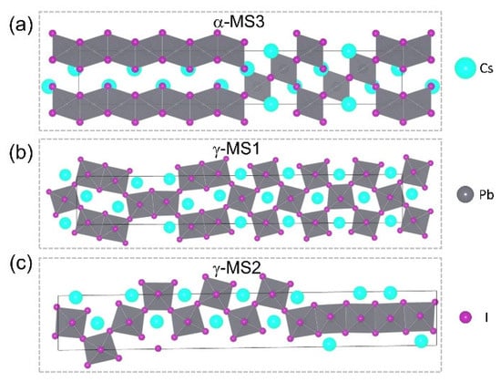
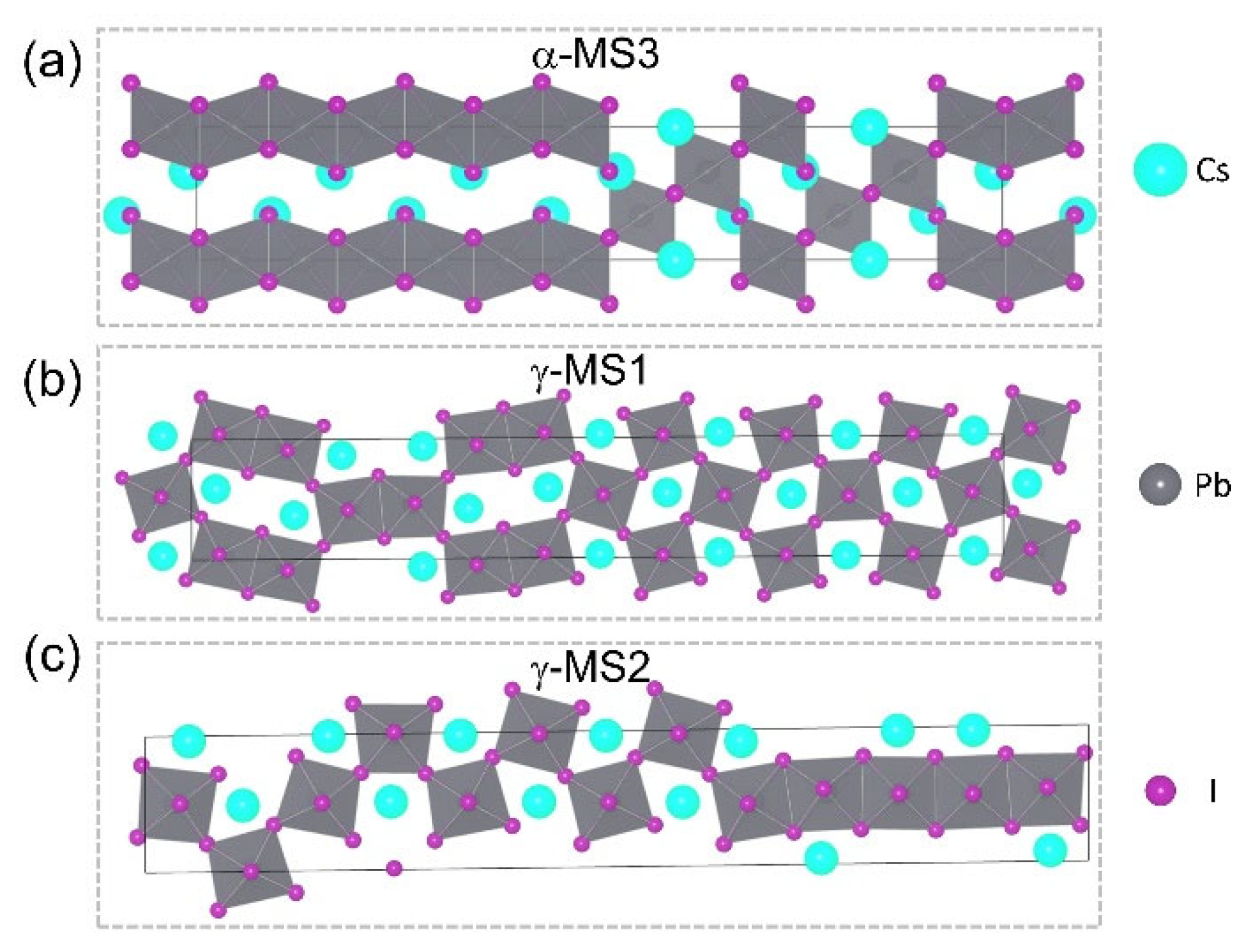
Previous research results have shown that the transformation of CsPbI3 from the perovskite to the non-perovskite phase requires a multi-step process involving three intermediate phases [12]. Other works constructed five CsPbI3 IB structures based on the key state structures in the phase transition in Refs. [12,16]. We selected three of these IB structures, as shown in Figure 1, namely α-MS3, γ-MS1, and γ-MS2. The primary screening criteria are rooted in their energy band alignments and relevance to photovoltaic applications. α-MS3, γ-MS1, and γ-MS2 were selected because they exhibit Type-II band alignment in the initial state, making them more suitable for photovoltaic applications, which are the main focus of this study. In the α-MS3 IB, the formation originates from the coplanarity of the (111)α plane and the (100)MS3 plane of the Cs-I sublattice; in the γ-MS1 and γ-MS2 IBs, the (100)γ plane remains coplanar with the (100)MS1 and (100)MS2 planes of the Cs-I sublattice, respectively.
Figure 1.
(a) α-MS3, (b) γ-MS1, and (c) γ-MS2 interphase boundary structures.
3. Results and Discussion
3.1. Effect of Pressure on Interphase Boundary Structures and IB Formation Energies
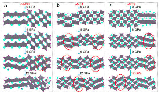
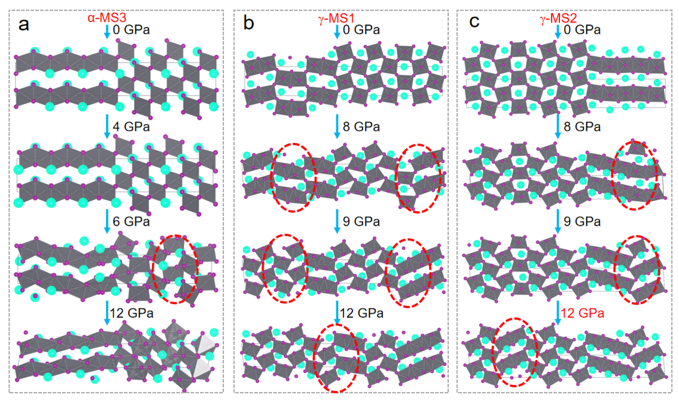
Figure 2 illustrates the pressure-induced structural evolution of α-MS3, γ-MS1, and γ-MS2 over the pressure range of 0-12 GPa, with four representative snapshots shown for each IB configuration. As depicted in Figure 2a, the α structure undergoes a noticeable lattice distortion at 6 GPa. Upon further compression to 12 GPa, a transition in the coordination environment of the Pb atoms is observed, where the coordination number of certain Pb species increases from six-fold to seven-fold. From Figure 2b, it is evident that after 8 GPa, the corner-sharing connectivity of PbI6 octahedra in γ-CsPbI3 is disrupted and transformed into edge-sharing connectivity; at 9 GPa and 12 GPa, some edge-sharing connections revert to corner-sharing. From Figure 2c, it can be clearly seen that after 8 GPa, the connectivity of PbI6 is disrupted, the edge-sharing long chains of PbI6 in the MS2 phase are broken, and some transform to corner-sharing connectivity; moreover, at 12 GPa, some corner-sharing PbI6 in the γ phase transform to edge-sharing. It should be noted that the present study is limited to the static high-pressure behavior of CsPbI3 interphase boundaries based on 0 K DFT calculations. Considering the connectivity of PbI6 is disrupted at high pressure, for α-MS3, γ-MS1, and γ-MS2, we subsequently investigate only the effects of pressure on their formation feasibility, band alignment, and optoelectronic properties within the ranges of 0–5 GPa, 0–7 GPa, and 0–7 GPa, respectively.
Figure 2.
Evolution of α-MS3 (a), γ-MS1 (b), and γ-MS2 (c) interphase boundary structures under different pressures. The red dashed circles highlight specific regions where the original corner-sharing continuous linkages of [PbI6] octahedra are disrupted or severely distorted due to applied pressure.
Formation feasibility of the material is one of the key indicators for assessing its potential for large-scale commercial application as an optoelectronic device material. Formation feasibility can be evaluated by calculating the interphase boundary formation energy (IBE), which is given by the following formula:
where EIB is the total energy of the IB system, EA and EB are the energies per unit cell of the two phases that constitute the IB, n and m are the corresponding numbers of unit cells, and S is the corresponding IB area. A smaller IBE indicates that the IB is more easily formed and the IB structure is more stable.
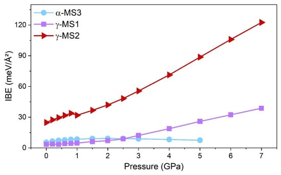
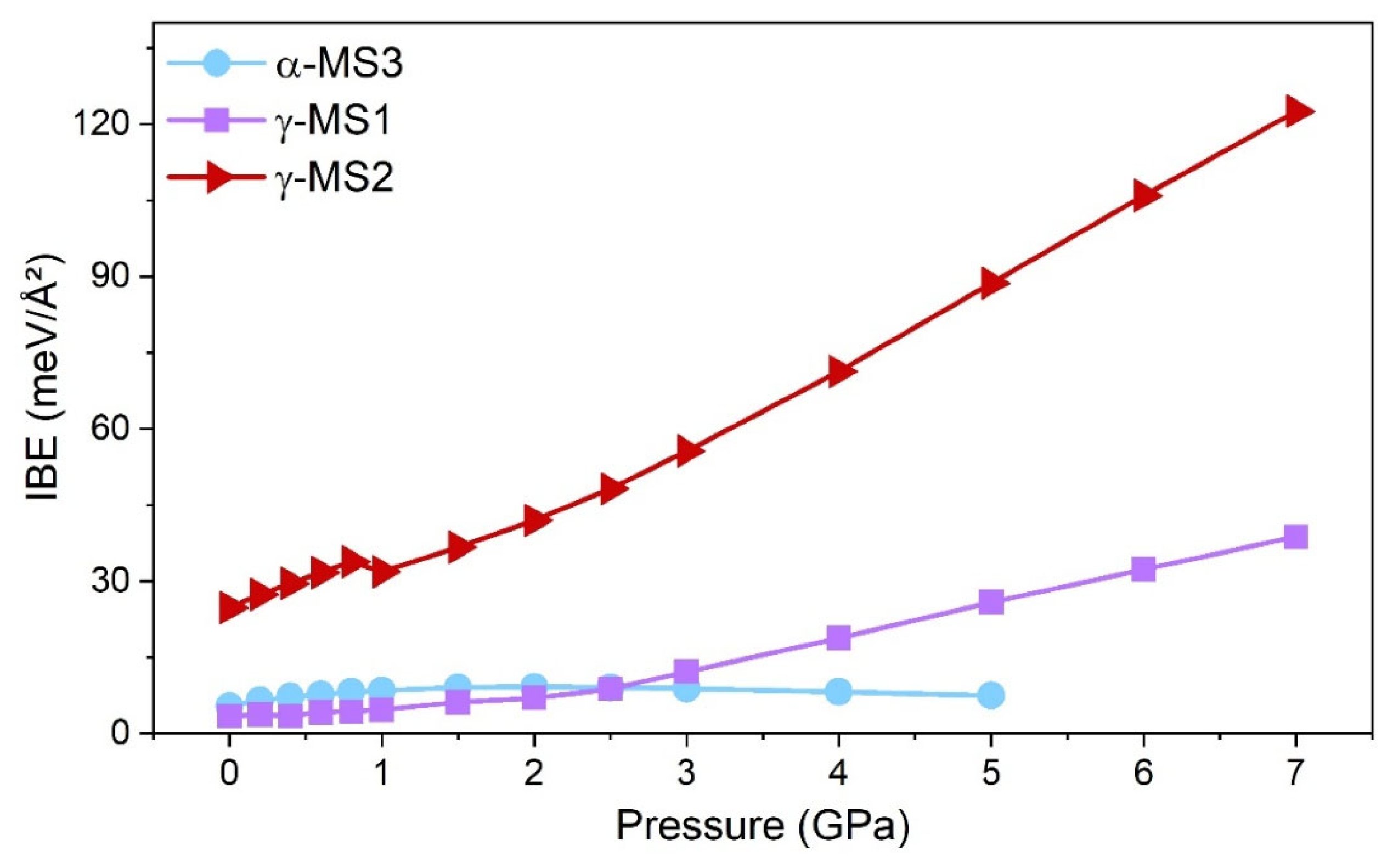
Figure 3 shows the pressure dependence of the IBE for the α-MS3, γ-MS1, and γ-MS2 IBs of CsPbI3. It can be seen that different IB conformations exhibit significantly different responses to pressure, reflecting a clear conformational dependence. Among them, γ-MS2 has the highest IBE throughout the entire pressure range (0–7 GPa) (red solid line with triangle symbols), and its IBE increases approximately linearly with increasing pressure, indicating that the formation of the γ-MS2 IB becomes difficult under applied pressure, and its formation feasibility decreases. In contrast, the IBE of γ-MS1 also increases monotonically with pressure (purple solid line with square symbols), but the overall increase is much smaller; especially within 3 GPa, the IBE of γ-MS1 changes relatively little, so pressure has a minor effect on its IB formation feasibility within this range. α-MS3 always maintains a relatively low IBE (blue solid line with circle symbols). Its IBE first increases slightly with pressure, but after exceeding 2 GPa, the IBE decreases. We attribute this primarily to the pressure-induced lattice distortion of the α structure under relatively high pressures. This structural evolution may promote a tendency toward the lower-energy β or γ phases, thereby contributing to the reduced IBE.
Figure 3.
Pressure dependence of the interphase boundary formation energies of α-MS3, γ-MS1, and γ-MS2.
Based on the results above, γ-MS2 has the highest IBE, the poorest formation feasibility, and is prone to destabilization upon pressure application. γ-MS1 is less affected by pressure within the range of less than 3 GPa, while the formation of the α-MS3 IB is barely affected by pressure; indeed, over a relatively large pressure range (2–5 GPa), the decrease in its IBE indicates an enhanced formation feasibility.
3.2. Evolution of Interphase Boundary Band Alignment and Its Mechanism
After the formation of an interphase boundary, due to the mismatched energy levels and interfacial charge transfer effects between the two crystalline phases, the valence band maximum and conduction band minimum usually exhibit discontinuities at the interface, i.e., valence band offset (VBO) and conduction band offset (CBO), leading to different band alignments. Specifically, these can be classified into Type-I, Type-II, or Type-III [41]. Generally, Type-I band alignments are suitable for light-emitting applications, whereas Type-II alignments—the central focus of this work—are often desirable for photovoltaic materials because they facilitate spatial charge separation. Type-III alignments, on the other hand, are typically characterized by broken-gap electronic structures and are potentially relevant to tunneling-related devices. Crucially, the band alignment type strongly influences the interfacial charge distribution, carrier recombination behavior, and the resulting optoelectronic performance. Thus, we calculated the band alignment relationships at the IBs under different pressures and analyzed the mechanism of band alignment transformation.
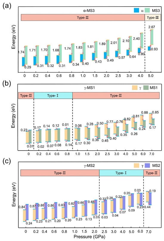
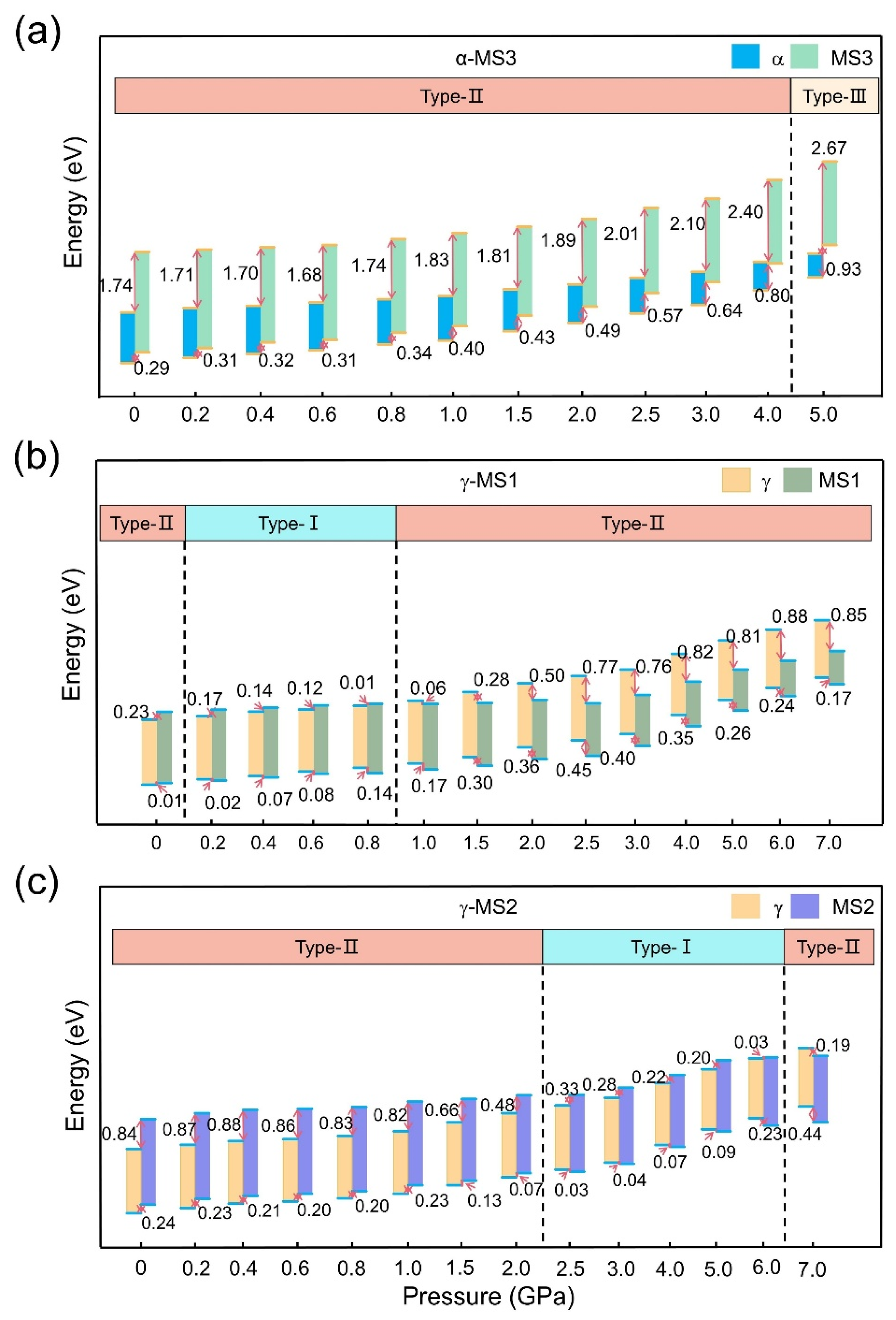
Figure 4 presents the band alignments and band offsets as functions of pressure for the three CsPbI3 IB structures studied herein. In the band alignment analysis, the 1s orbital of iodine atoms far from the IB was used as the core-level reference, and the VBO and CBO on both sides of the IB were determined using the core-level alignment method [42]. From Figure 4a, it can be seen that within the range of 0–4.0 GPa, both the conduction band minimum (CBM) and valence band maximum (VBM) of MS3 (light green rectangle) are higher than those of α (blue rectangle), forming a staggered Type-II band alignment. Electrons tend to migrate from MS3 to α, whereas holes tend to transfer in the opposite direction, from α to MS3. This spatial separation of photogenerated electron–hole pairs is expected to reduce carrier recombination, making this configuration promising for photodetectors and photovoltaic applications. As pressure increases, the CBO gradually increases from 1.74 eV to 2.40 eV, and the VBO increases from 0.29 eV to 0.80 eV, indicating that the band edge misalignment on both sides of the IB continuously strengthens, and the interface’s selective separation capability for electrons and holes continues to improve. This pressure-enhanced band offset helps suppress reverse migration and recombination of electrons and holes at the interface, improving the lifetime and separation efficiency of photogenerated carriers. When the pressure increases to 5 GPa, the band alignment of the α-MS3 IB transforms from Type-II to Type-III, where the VBM of one component straddles the CBM of the other component, forming a typical broken-gap band alignment. This specific alignment establishes an energetically favorable band profile that may facilitate interband tunneling across the interface. Thus, at pressure higher than 5 GPa, the α-MS3 IB has potential for application in high-frequency, low-power tunneling electronic devices.
Figure 4.
Evolution of band alignments under different pressures for (a) α-MS3, (b) γ-MS1, and (c) γ-MS2.
From Figure 4b, at ambient pressure, the γ-MS1 IB exhibits Type-II band alignment. As the pressure increases from 0 to 7 GPa, the CBM/VBM of γ (yellow rectangle) continuously shifts upward relative to MS1 (green rectangle), indicating that pressure can significantly modulate the relative band edge positions on both sides of the interface. At 0.2 GPa, the band alignment changes from the initial Type-II to Type-I. In the range of 0.2–0.8 GPa, γ-MS1 remains in Type-I. In this alignment, both electrons and holes tend to migrate from MS1 to the γ phase and accumulate on the same side, which is more favorable for carrier recombination but not for electron–hole spatial separation. This suggests that γ-MS1 in this pressure range is more suitable as a light-emitting material. As the pressure increases further, the CBM and VBM of γ continue to shift upward. At 1.0 GPa, both band edges of γ shift above the corresponding band edges of MS1, causing the γ-MS1 alignment to return to a Type-II configuration. In the range of 1.0–7.0 GPa, the CBO continuously increases from 0.06 eV to 0.85 eV, indicating that the distribution difference in electrons on both sides of the interface continuously increases. In contrast, the VBO rises from 0.17 eV to a maximum of 0.45 eV at 2.5 GPa and then gradually decreases to 0.17 eV at 7.0 GPa.
From Figure 4c, as the pressure increases from 0 to 7 GPa, the CBM/VBM of γ continuously shifts upward relative to MS2, indicating that pressure can significantly modulate the relative band edge positions on both sides of the γ-MS2 IB. In the range of 0–2.0 GPa, γ-MS2 maintains Type-II; however, the CBO gradually decreases from 0.84 to 0.48 eV, accompanied by a reduction in the VBO from 0.24 to 0.07 eV. This simultaneous decrease weakens the energetic driving force for spatially separating photogenerated carriers, which may limit charge separation and thus affect the overall optoelectronic or photovoltaic performance. As the pressure further increases to 2.5 GPa, the CBO continues to decrease to 0.33 eV. Although the CBM of γ is still lower than that of MS2, its VBM has risen to be higher than that of MS2, causing γ-MS2 to transform to Type-I. In the range of 2.5–6.0 GPa, the system maintains Type-I. When the pressure continues to increase to 7.0 GPa, the CBM of γ further rises and exceeds that of MS2, and the system reverts to Type-II. It is worth noting that although both 0–2.0 GPa and 7.0 GPa show Type-II, the carrier migration directions are opposite. In the range of 0–2.0 GPa, electrons migrate from MS2 to the γ phase, while holes transfer from γ to MS2; at 7.0 GPa, the migration directions of electrons and holes are reversed. This suggests that pressure not only induces transitions between Type-II and Type-I in the γ-MS2 IB but also further modulates the carrier flow direction.
Combining the results for the γ-MS1, γ-MS2, and α-MS3 IB systems, it is clear that pressure can effectively modulate the relative band edge positions and band alignments on both sides of different CsPbI3 IBs, and further affect the interfacial carrier separation, recombination, and transport behavior. As pressure varies, the system can transition among Type-I, Type-II, and even Type-III band alignments, corresponding to diverse potential device functions, including light emission for Type-I, photovoltaics for Type-II, and tunneling-related electronic applications for Type-III. Therefore, pressure provides an effective approach to achieving multifunctional property regulation within a single CsPbI3 material system and offers a theoretical basis for the design and application expansion of multifunctional optoelectronic devices.
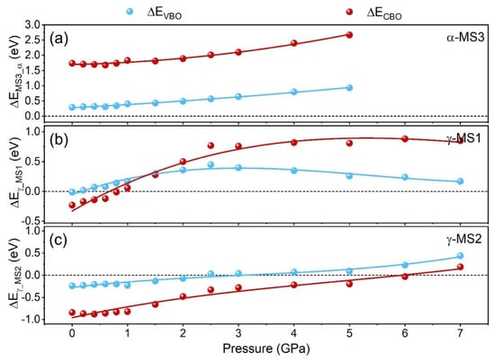
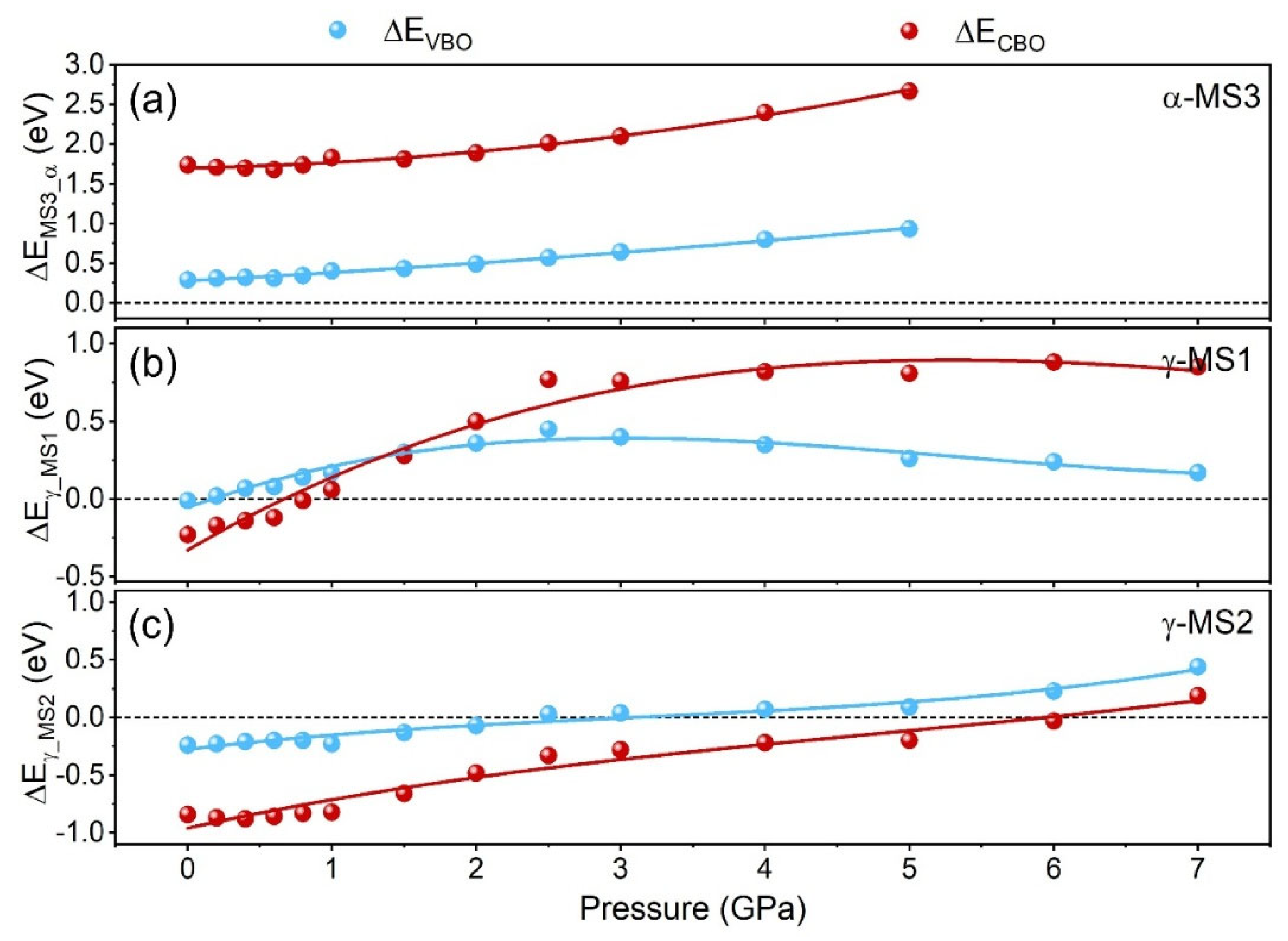
To further analyze the reasons for the band alignment transitions in the three types of IBs, the pressure dependence of the VBO and CBO is examined. Figure 5 shows the evolution of VBO and CBO on both sides of the α-MS3, γ-MS1, and γ-MS2 IBs with pressure. For the α-MS3 IB (Figure 5a), the VBO and CBO corresponding to the MS3 side relative to the α side increase monotonically with increasing pressure, indicating that the band edges on the MS3 side are more sensitive to pressure, shifting upward faster than those on the α side, thereby causing the band alignment of the α-MS3 IB to gradually change from Type-II to Type-III. For the γ-MS1 IB (Figure 5b), the VBO changes from negative to positive at 0.2 GPa, corresponding to a transition from Type-II to Type-I. As the pressure further increases, the CBO also changes from negative to positive at 1.0 GPa, causing the band alignment to revert from Type-I to Type-II. Thus, in the γ-MS1 IB, the band edges of the γ phase exhibit a stronger response to pressure, and its CBM shows higher pressure sensitivity than its VBM. For the γ-MS2 IB (Figure 5c), the VBO changes from negative to positive near 2.5 GPa, corresponding to a transition from Type-II to Type-I for γ-MS2; when the pressure further increases to 6.0 GPa, the CBO also changes from negative to positive, causing the band alignment to revert from Type-I to Type-II. Unlike the γ-MS1 IB, the VBM and CBM of the γ phase in γ-MS2 have relatively similar pressure responses, indicating that its valence and conduction bands shift relatively synchronously under pressure.
Figure 5.
VBO and CBO between the two sides of (a) α−MS3, (b) γ−MS1, and (c) γ−MS2 IBs under different pressures. ΔEα−MS3, ΔEγ−MS1, and ΔEγ−MS2 denote the VBM/CBM energy differences in MS3 relative to α, γ relative to MS1 and MS2, respectively. The black dashed line indicates the zero energy difference.
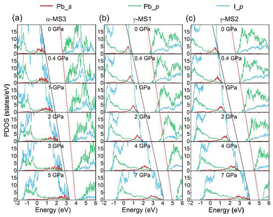
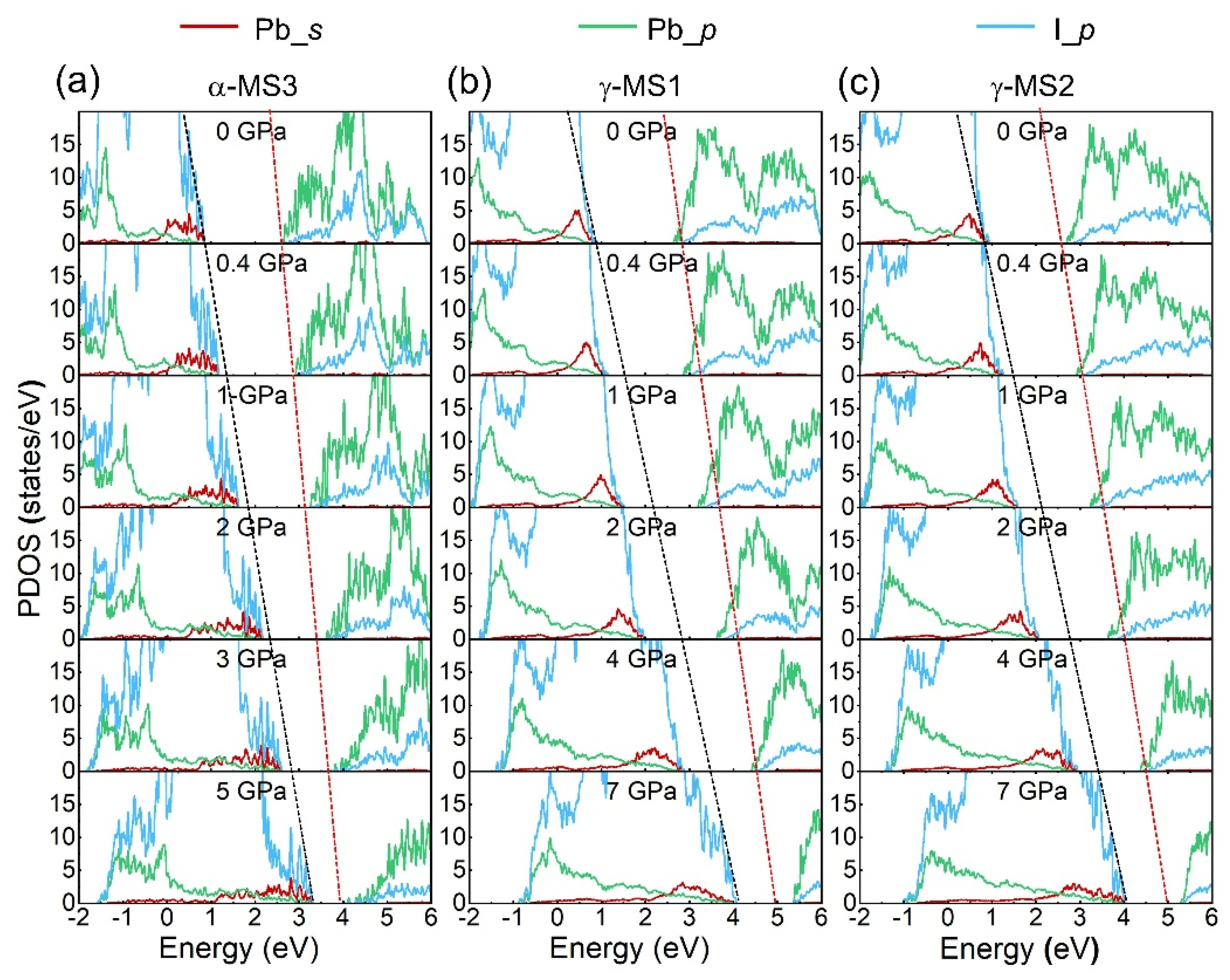
To further reveal the mechanism underlying the evolution of the IB band alignment, the orbital composition of the VBM and CBM, and the origin of the pressure-induced electronic structure changes are analyzed using partial density of states (PDOS). Figure 6 shows the PDOS of the three IB structures studied herein. To facilitate observation of the pressure-induced shifts in the VBM and CBM for the three IB structures, the Fermi level is kept at its original value. From Figure 6, it can be seen that the VBM of α-MS3, γ-MS1, and γ-MS2 is mainly contributed by Pb_s and I_p orbitals, while the CBM is mainly contributed by Pb_p and a small amount of I_p orbitals. Therefore, the effect of pressure on the band edge structure mainly influences the distribution of orbital electrons of Pb and I elements. By comparing the slopes of the black dashed line and the red dashed line, we can observe that the VBM is more strongly affected by pressure. This is mainly due to the compression enhancing Pb–I orbital overlap and altering the local distortion of PbI6 octahedra. The unoccupied CBM also shifts to a higher energy but is less affected by pressure. Combining the insights from Figure 5 and Figure 6, we find that the band edge structures of MS3 and γ exhibit a higher sensitivity to hydrostatic pressure. This phenomenon primarily originates from the fact that their Pb–I bond lengths and PbI6 octahedral configurations are more susceptible to external pressure, which consequently enhances the hybridization between the Pb_s/p and I_p orbitals. Among them, the I_p/Pb_s antibonding states near the VBM and the Pb_p/I_p hybrid states near the CBM are both affected, causing changes in band edge positions and band offsets. Due to the different local structures and compression responses of the crystalline phases on both sides of the IB, pressure does not modulate the Pb-I bond lengths, octahedral distortions, and the strength of Pb-I orbital hybridization in a consistent manner, leading to different magnitudes of shift for the VBM and CBM on the two sides, ultimately altering the VBO, CBO, and band alignment type at the IB, thereby inducing the band alignment transitions shown in Figure 4 for the three IB structures.
Figure 6.
Partial density of states (PDOS) of (a) α−MS3, (b) γ−MS1, and (c) γ−MS2 under different pressures. The dark red, dark green, and light blue curves represent contributions from Pb_s, Pb_p, and I_p orbitals, respectively. The black and red dashed lines serve as guides to the eye, tracing the shift trends of VBM and CBM, respectively, with increasing pressure.
In Figure 6, the slope of the black dashed line is steeper than that of the red dashed line, i.e., the VBM shifts toward higher energies faster than the CBM, causing the bandgap of the three IBs to continuously decrease. Bandgap is one of the key parameters affecting the photovoltaic conversion efficiency of a material. We focus on the application of CsPbI3 IB structures in the field of solar cells. Therefore, the optoelectronic properties of IB structures with Type-II are further studied.
3.3. Effect of Pressure on the Optoelectronic Properties of Interphase Boundaries
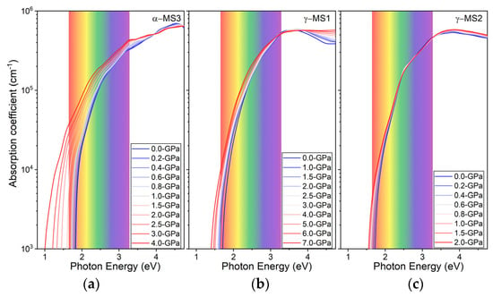
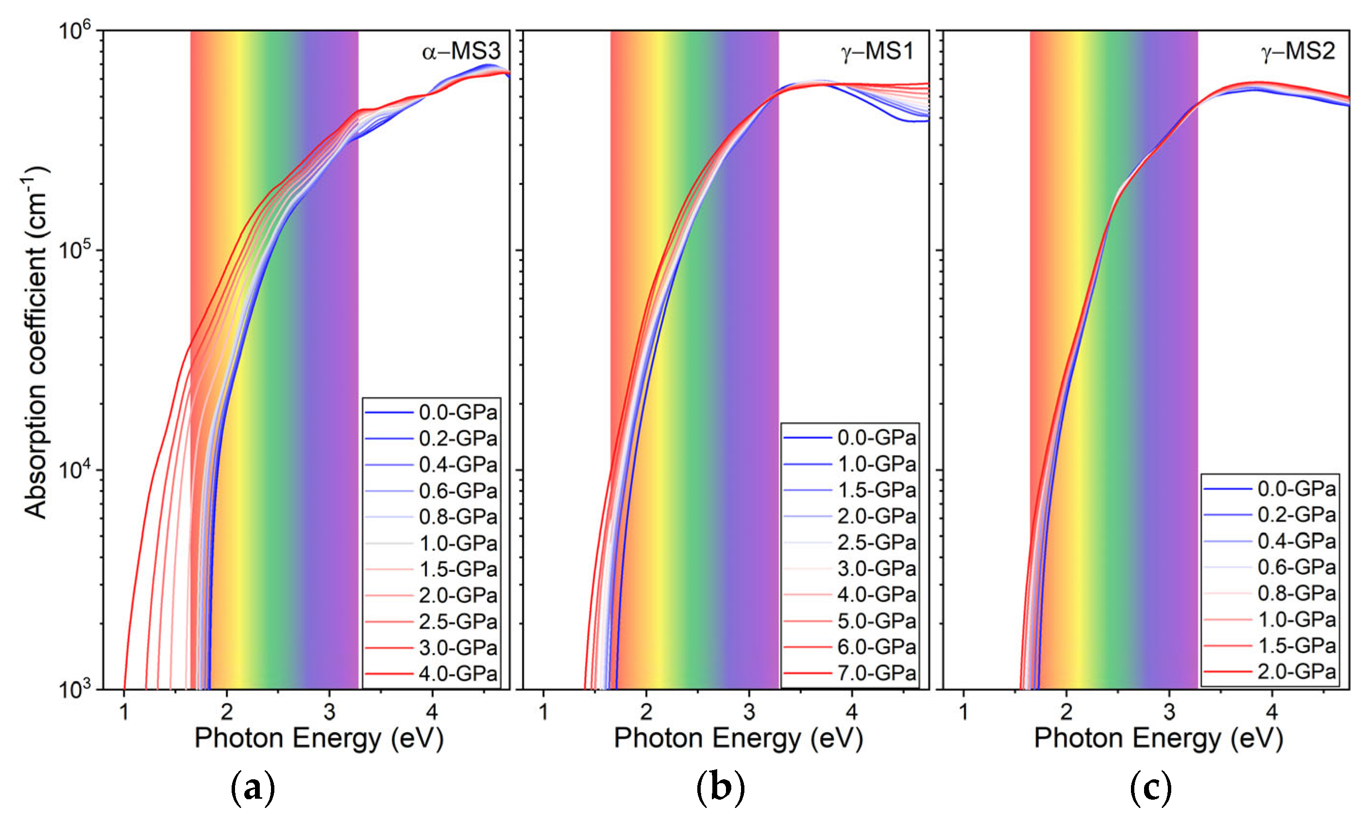
Figure 7 shows the optical absorption coefficients of the three CsPbI3 IBs. As this work focuses on IB structures with Type-II, the optical absorption coefficients for α-MS3 under 0–4 GPa, for γ-MS1 under 0 GPa and 1–7 GPa, and for γ-MS2 under 0–2 GPa were calculated according to Figure 4. The photon energy of visible light is approximately 1.7 eV to 3.2 eV, which covers most of the solar spectrum. From Figure 7, it can be seen that the optical absorption coefficients of the three IB structures reach a high order of magnitude of 104–105 cm−1 in the visible range. Moreover, with increasing pressure, the optical absorption coefficients of the three CsPbI3 IBs in the visible range show an increasing trend. This indicates that pressure enhances the absorption capability of the IBs for visible light, which corresponds to the fact that pressure reduces the bandgap of the CsPbI3 IBs (Figure 6).
Figure 7.
Optical absorption coefficients of (a) α−MS3, (b) γ−MS1, and (c) γ−MS2 under different pressures.
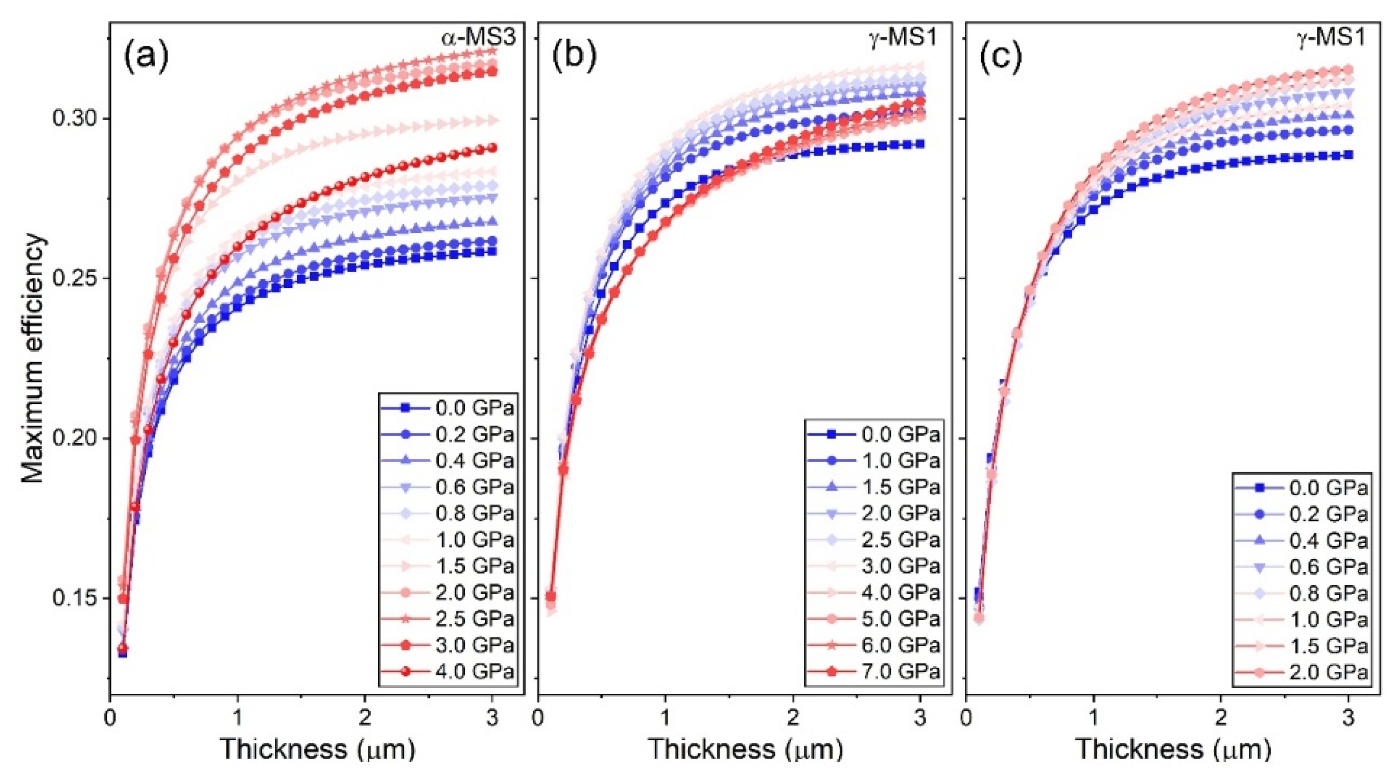
Although the optical absorption coefficient reflects the light-harvesting capability of CsPbI3 interphase boundaries, it does not directly determine the device-level photovoltaic performance, which also depends on carrier separation, transport, and recombination processes. A more comprehensive figure of merit for solar cell applications is the spectroscopic-limited maximum efficiency (SLME), which integrates the absorption profile, the bandgap value, and the material thickness under the detailed balance framework. Therefore, we further evaluate the SLME of the three IBs under different pressures.
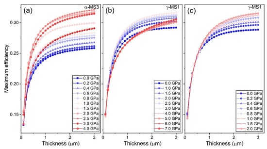
Figure 8 shows the pressure dependence of the SLME for the three CsPbI3 IB structures. For α-MS3, γ-MS1, and γ-MS2, they achieve a relatively high conversion efficiency at a thickness of 1 μm, meaning that a small film thickness can achieve efficient absorption and conversion of sunlight. For α-MS3, the highest conversion efficiency is achieved at a pressure of 2.5 GPa. This result is mainly attributed to the fact that at 2.5 GPa, the bandgap of α-MS3 is 1.295 eV, which is closest to the optimal bandgap of 1.34 eV corresponding to the Shockley–Queisser theoretical limit efficiency. For γ-MS1, the highest conversion efficiency is achieved at 3.0 GPa, while for γ-MS2, the highest conversion efficiency is achieved at 2 GPa. For photovoltaic absorber design, a thickness of 1.5–2 μm may provide a reasonable balance between light-harvesting efficiency and material usage. Within this thickness range, the predicted SLME approaches the saturation trend with increasing thickness, but it does not necessarily reach the true large-thickness saturation limit, which generally requires a thicker absorber layer; further increasing the absorber layer thickness provides limited improvement in efficiency and may instead increase recombination probability due to longer carrier transport paths. Therefore, pressure is an effective means to optimize the photovoltaic properties of CsPbI3 materials.
Figure 8.
SLME of (a) α-MS3, (b) γ-MS1, and (c) γ-MS2 under different pressures.
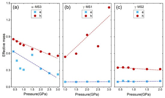
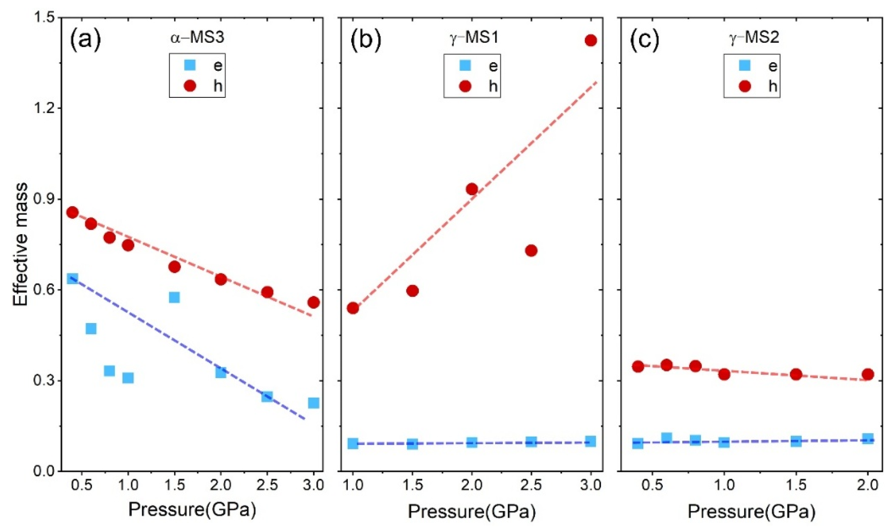
Carrier effective mass is one of the key parameters for evaluating the photovoltaic conversion performance, as it significantly affects carrier mobility and collection efficiency. Figure 9 shows the pressure dependence of the carrier effective masses for the three CsPbI3 IBs. Based on the results in Figure 8, only the carrier effective masses in the range of 0.4 GPa to 3.0 GPa were calculated. For α-MS3 (Figure 9a), as pressure increases, both the electron and hole effective masses decrease significantly, indicating that the mobility and transport efficiency of photogenerated carriers are enhanced. For CsPbI3-based solar cells, this facilitates faster transport of photogenerated electrons and holes and their efficient collection by the electrodes, thereby suppressing carrier recombination and ultimately improving the photovoltaic conversion efficiency. For γ-MS1 (Figure 9b), as pressure increases, the electron effective mass remains essentially stable (below 0.15 m0), while the hole effective mass increases significantly. This indicates that electron transport in this system is less affected by pressure, while hole transport capability is significantly weakened. It further reveals that increasing pressure does not significantly improve electron transport properties; instead, the decrease in hole mobility may weaken the synergistic transport and separation efficiency of carriers, thereby limiting further improvement of its photovoltaic conversion performance. For γ-MS2 (Figure 9c), the electron effective mass remains unchanged, the hole effective mass decreases slightly, and both electron and hole effective masses are always below 0.45 m0, indicating that this system maintains excellent ambipolar carrier transport capability under pressure, which is beneficial for carrier separation, migration, and collection.
Figure 9.
Electron and hole effective masses of (a) α-MS3, (b) γ-MS1, (c) and γ-MS2 under different pressures.
4. Conclusions
In this work, we systematically investigated the effects of pressure on the formation feasibility, band alignments, and optoelectronic properties of three CsPbI3 IBs, namely α-MS3, γ-MS1, and γ-MS2. Pressure significantly influences IB formation feasibility by modulating the PbI6 octahedral distortions, connectivity, and local strain states. Among them, the IB formation energy of γ-MS2 increases approximately linearly with pressure, indicating relatively weak formation feasibility; γ-MS1 exhibits a small change in IB formation energy within 3 GPa, showing good formation feasibility; the IB formation energy of α-MS3 decreases in the range of 2–5 GPa, suggesting that moderate pressure is beneficial for its stability. Analysis of band alignments shows that pressure can effectively modulate the band alignment at the IBs. α-MS3 maintains Type-II within 0–4 GPa, favorable for electron–hole spatial separation and transforms to Type-III at 5 GPa; γ-MS1 and γ-MS2 exhibit an evolution of Type-II → Type-I → Type-II, indicating that pressure can selectively regulate carrier separation, migration, and recombination processes. This behavior essentially originates from the fact that pressure does not uniformly modulate the Pb–I bond lengths, octahedral distortions, and the strength of Pb_p/Pb_s with I_p orbital hybridization, leading to changes in the VBO, CBO, and band alignment on both sides. Further optoelectronic property analysis shows that the Type-II IBs of CsPbI3 exhibit absorption coefficients on the order of 104–105 cm−1 in the visible region. Moderate pressure can enhance optical absorption and spectroscopic-limited maximum conversion efficiency via bandgap engineering and improve carrier transport performance. Overall, pressure provides an effective means for the synergistic regulation of the formation feasibility, band alignments, and optoelectronic properties of CsPbI3 IBs, offering theoretical guidance for the design of multifunctional perovskite optoelectronic materials.
Author Contributions
Conceptualization, G.C. and C.M.; methodology, C.H.; validation, X.Z.; investigation, C.L. and Y.W.; data curation, X.S.; writing—original draft preparation, X.S. and G.C.; writing—review and editing, H.L. and C.M. All authors have read and agreed to the published version of the manuscript.
Funding
National Natural Science Foundation of China (Grant No. 52302298); Postgraduate Research &Practice Innovation Program of Jiangsu Province, No. KYCX24_3413.
Informed Consent Statement
Not applicable.
Data Availability Statement
The data that support the findings of this study are available from the corresponding authors upon reasonable request.
Conflicts of Interest
The authors declare no conflicts of interest.
Abbreviations
The following abbreviations are used in this manuscript:
| IBs | Interphase Boundaries |
| IBE | Interphase Boundary Energy |
| VBM | Valence Band Maximum |
| CBM | Conduction Band Minimum |
| SLME | Spectroscopic Limited Maximum Efficiency |
References
- Wang, Y.; Dar, M.I.; Ono, L.K.; Zhang, T.; Kan, M.; Li, Y.; Zhang, L.; Wang, X.; Yang, Y.; Gao, X.; et al. Thermodynamically stabilized β-CsPbI3–based perovskite solar cells with efficiencies > 18%. Science 2019, 365, 591–595. [Google Scholar] [CrossRef] [Scilit]
- Qiu, J.; Mei, X.; Zhang, M.; Wang, G.; Zou, S.; Wen, L.; Huang, J.; Hua, Y.; Zhang, X. Dipolar chemical bridge induced CsPbI3 perovskite solar cells with 21.86% efficiency. Angew. Chem. 2024, 136, e202401751. [Google Scholar] [CrossRef] [Scilit]
- Pintor Monroy, M.I.; Goldberg, I.; Elkhouly, K.; Georgitzikis, E.; Genoe, J. All-evaporated, all-inorganic CsPbI3 Perovskite-based devices for broad-band photodetector and solar cell applications. ACS Appl. Electron. Mater. 2021, 3, 3023–3033. [Google Scholar] [CrossRef] [Scilit] [PubMed]
- Wei, H.; Ji, X.; Cao, J.; He, W.; Liu, H.; Pan, Z.; Song, X.; Sun, Q.; Li, J.; Wu, C. High-Performance CsPbI3 Quantum Dot Photodetector with a Vertical Structure Based on the Frenkel–Poole Emission Effect. ACS Nano 2024, 18, 26643–26654. [Google Scholar] [CrossRef] [Scilit] [PubMed]
- Weng, J.; Xu, M.; Wang, X.; Wang, F.; Shen, J.; Zhang, B. Self-powered, ultraviolet-to-near infrared broadband photodetector based on Ag-doped CsPbI3/PEDOT: PSS heterojunction. Opt. Express 2022, 30, 37261–37271. [Google Scholar] [CrossRef] [Scilit]
- Li, Y.; Deng, M.; Zhang, X.; Xu, T.; Wang, X.; Yao, Z.; Wang, Q.; Qian, L.; Xiang, C. Stable and efficient CsPbI3 quantum-dot light-emitting diodes with strong quantum confinement. Nat. Commun. 2024, 15, 5696. [Google Scholar] [CrossRef] [Scilit]
- Litvin, A.P.; Guo, J.; Wang, J.; Zhang, X.; Zheng, W.; Rogach, A.L. Systematic Study of the Synthesis of Monodisperse CsPbI3 Perovskite Nanoplatelets for Efficient Color-Pure Light Emitting Diodes. Small 2025, 21, 2408422. [Google Scholar] [CrossRef] [Scilit]
- Hussein, S.I.; Ismail, R.A.; Almashhadani, N.J.; Addie, A.J. Laser pulse tuning for optimized photodetector performance in CsPbI3/Si heterojunctions. Opt. Quantum Electron. 2024, 57, 64. [Google Scholar] [CrossRef] [Scilit]
- Shang, X.; Xu, N.; Zong, M.; Yu, W.; Guo, L.; Gao, G.; Zhang, Z.; Zhang, H.; Su, L. ZrGeTe4 Nanoparticles as a Saturable Absorber for Mode-Locked Operations at 1 and 1.55 µm. Photonics 2026, 13, 305. [Google Scholar] [CrossRef] [Scilit]
- Marronnier, A.; Roma, G.; Boyer-Richard, S.; Pedesseau, L.; Jancu, J.M.; Bonnassieux, Y.; Katan, C.; Stoumpos, C.C.; Kanatzidis, M.G.; Even, J. Anharmonicity and disorder in the black phases of cesium lead iodide used for stable inorganic perovskite solar cells. ACS Nano 2018, 12, 3477–3486. [Google Scholar] [CrossRef] [Scilit]
- Zhao, B.; Jin, S.F.; Huang, S.; Liu, N.; Ma, J.Y.; Xue, D.J.; Han, Q.; Ding, J.; Ge, Q.Q.; Feng, Y.; et al. Thermodynamically stable orthorhombic γ-CsPbI3 thin films for high-performance photovoltaics. J. Am. Chem. Soc. 2018, 140, 11716–11725. [Google Scholar] [CrossRef] [Scilit]
- Chen, G.Y.; Guo, Z.D.; Gong, X.G.; Yin, W.J. Kinetic pathway of γ-to-δ phase transition in CsPbI3. Chem 2022, 8, 3120–3129. [Google Scholar] [CrossRef] [Scilit]
- Zhang, L.; Guo, T.; Liu, B.; Du, D.; Xu, S.; Zheng, H.; Zhu, L.; Pan, X.; Liu, G. Intermediate-phase-modified crystallization for stable and efficient CsPbI3 perovskite solar cells. ACS Appl. Mater. 2022, 14, 19614–19622. [Google Scholar] [CrossRef] [Scilit]
- Chen, J.; Wang, J.; Xu, X.; Li, J.; Song, J.; Lan, S.; Liu, S.; Cai, B.; Han, B.; Precht, J.T.; et al. Efficient and bright white light-emitting diodes based on single-layer heterophase halide perovskites. Nat. Photonics 2021, 15, 238–244. [Google Scholar] [CrossRef] [Scilit]
- Zhao, H.; Xu, J.; Zhou, S.; Li, Z.; Zhang, B.; Xia, X.; Liu, X.; Dai, S.; Yao, J. Preparation of Tortuous 3D γ-CsPbI3 Films at Low Temperature by CaI2 as Dopant for Highly Efficient Perovskite Solar Cells. Adv. Funct. Mater. 2019, 29, 1808986. [Google Scholar] [CrossRef] [Scilit]
- Chen, X.; Chen, G.; Yin, W.J. Interphase boundaries and their impact on carrier dynamics in lead halide perovskites. J. Phys. Chem. Lett. 2023, 14, 6459–6463. [Google Scholar] [CrossRef] [Scilit]
- Kweon, K.E.; Varley, J.; Ogitsu, T.; Wan, L.; Shelby, M.; Song, Z.; Ellingson, R.J.; Yan, Y.; Lee, J.R.I. Influence of external conditions on the black-to-yellow phase transition of CsPbI3 based on first-principles calculations: Pressure and moisture. Chem. Mater. 2023, 35, 2321–2329. [Google Scholar] [CrossRef] [Scilit]
- Lyu, H.; Su, H.; Lin, Z. Two-stage dynamic transformation from δ-to α-CsPbI3. J. Phys. Chem. Lett. 2024, 15, 2228–2232. [Google Scholar] [CrossRef] [Scilit]
- Holley, R., III; Burlingame, Q.C.; Loo, Y.-L. Mapping the polymorphic phase transformations of CsPbI3 perovskite thin films. J. Mater. Chem. C 2025, 13, 19654–19659. [Google Scholar] [CrossRef] [Scilit]
- Kaiser, W.; Hussain, K.; Singh, A.; Alothman, A.A.; Meggiolaro, D.; Gagliardi, A.; Mosconi, E.; De Angelis, F. Defect formation and healing at grain boundaries in lead-halide perovskites. J. Mater. Chem. A 2022, 10, 24854–24865. [Google Scholar] [CrossRef] [Scilit]
- Liu, R.; Wang, F.; Liu, L.; He, X.; Chen, J.; Li, Y.; Zhai, T. Band alignment engineering in two-dimensional transition metal dichalcogenide-based heterostructures for photodetectors. Small Struct. 2021, 2, 2000136. [Google Scholar] [CrossRef] [Scilit]
- Wang, C.; Zhang, H.; Wei, Y.; Li, P.; Lin, P.; Liu, T.; Wu, X.; Wang, P.; Yu, X.; Ni, Z.; et al. Reinforcing CsPbI3 all-inorganic perovskite grain boundaries through bilateral cyano-based molecular cross-linking for efficient and stable solar cells. Appl. Phys. Lett. 2026, 128, 153905. [Google Scholar] [CrossRef] [Scilit]
- Liu, N.; Liu, Z.; Wang, J.; Ye, Q.; Wang, Y.; Han, W.; Xu, W.; Zhang, J.; Huang, L.; Hu, Z.; et al. Synchronous surface reconstruction and grain boundary healing toward efficient and stable inverted CsPbI3 perovskite solar cells. Chem. Eng. J. 2024, 485, 149590. [Google Scholar] [CrossRef] [Scilit]
- Guo, J.; Wang, Y.; Guo, H.; Ren, X.; Ning, X.; Wei, J.; Yang, H.; Li, T.; Zhu, C.; Hou, F. Modulating secondary growth of perovskite grains through residual solvent evaporation. Opt. Express 2024, 32, 19645–19654. [Google Scholar] [CrossRef] [Scilit] [PubMed]
- Hu, L.; Xu, C.; Sun, H.; Wang, H.; Yu, L.; Yang, J.; Cheng, F.; Kang, Z.; Zhang, Y. Pushing the performance of inverted CsPbI3 perovskite photovoltaics via grain boundary grooves stitching. Joule 2026, 10, 102319. [Google Scholar] [CrossRef] [Scilit]
- Wylie, Z.R.; Al Katrib, M.; Campagna, R.; Outen, J.E.; Smith, S.; Ruffolo, P.; Bérenguier, B.; Bouttemy, M.; Schulz, P.; Christians, J.A. Surface iodide defects control the kinetics of the CsPbI3 perovskite phase transformation. ACS Energy Lett. 2024, 9, 4378–4385. [Google Scholar] [CrossRef] [Scilit] [PubMed]
- Yoon, G.W.; Lee, S.R.; Park, S.E.; Ahn, H.; Lee, D.K.; Gong, O.Y.; Han, G.S.; Sutter-Fella, C.M.; Lee, B.R.; Jung, H.S.; et al. Tailoring the Intermediate Phase to Control Formation of γ-CsPbI3 Films. ACS Energy Lett. 2025, 10, 6104–6113. [Google Scholar] [CrossRef] [Scilit]
- Mali, S.S.; Patil, J.V.; Shao, J.Y.; Zhong, Y.W.; Rondiya, S.R.; Dzade, N.Y.; Hong, C.K. Phase-heterojunction all-inorganic perovskite solar cells surpassing 21.5% efficiency. Nat. Energy 2023, 8, 989–1001. [Google Scholar] [CrossRef] [Scilit]
- Guo, Z.; Wang, J.; Yin, W.J. Atomistic origin of lattice softness and its impact on structural and carrier dynamics in three dimensional perovskites. Energy Environ. Sci. 2022, 15, 660–671. [Google Scholar] [CrossRef] [Scilit]
- Xu, K.; Pérez-Fidalgo, L.; Charles, B.L.; Weller, M.T.; Alonso, M.I.; Goñi, A.R. Using pressure to unravel the structure–dynamic-disorder relationship in metal halide perovskites. Sci. Rep. 2023, 13, 9300. [Google Scholar] [CrossRef] [Scilit]
- Ke, F.; Wang, C.; Jia, C.; Wolf, N.R.; Yan, J.J.; Niu, S.Y.; Devereaux, T.P.; Karunadasa, H.I.; Mao, W.L.; Lin, Y. Preserving a robust CsPbI3 perovskite phase via pressure-directed octahedral tilt. Nat. Commun. 2021, 12, 461. [Google Scholar] [CrossRef] [Scilit] [PubMed]
- Saikia, D.; Alam, M.; Das, C.; Betal, A.; Gandi, A.N.; Sahu, S. Pressure induced structural, electronic and optical properties of CsPbI3 perovskite. New J. Chem. 2024, 48, 20225–20233. [Google Scholar] [CrossRef] [Scilit]
- Wang, J.; Wang, L.; Li, Y.; Fu, R.J.; Feng, Y.J.; Chang, D.H.; Yuan, Y.F.; Gao, H.; Jiang, S.; Wang, F.; et al. Pressure-induced metallization of lead-free halide double perovskite (NH4)2PtI6. Adv. Sci. 2022, 9, 2203442. [Google Scholar] [CrossRef] [Scilit]
- Hohenberg, P.; Kohn, W. Inhomogeneous electron gas. Phys. Rev. 1964, 136, B864. [Google Scholar] [CrossRef] [Scilit]
- Perdew, J.P.; Burke, K.; Ernzerhof, M. Generalized gradient approximation made simple. Phys. Rev. Lett. 1996, 77, 3865. [Google Scholar] [CrossRef] [Scilit]
- Kresse, G.; Furthmüller, J. Efficiency of ab-initio total energy calculations for metals and semiconductors using a plane-wave basis set. Comput. Mater. Sci. 1996, 6, 15–50. [Google Scholar] [CrossRef] [Scilit]
- Kresse, G.; Furthmüller, J. Efficient iterative schemes for ab initio total-energy calculations using a plane-wave basis set. Phys. Rev. B 1996, 54, 11169. [Google Scholar] [CrossRef] [Scilit]
- Monkhorst, H.J.; Pack, J.D. Special points for Brillouin-zone integrations. Phys. Rev. B 1976, 13, 5188. [Google Scholar] [CrossRef] [Scilit]
- Wang, V.; Xu, N.; Liu, J.-C.; Tang, G.; Geng, W.T. VASPKIT: A user-friendly interface facilitating high-throughput computing and analysis using VASP code. Comput. Phys. Commun. 2021, 267, 108033. [Google Scholar] [CrossRef] [Scilit]
- Momma, K.; Izumi, F. VESTA 3 for three-dimensional visualization of crystal, volumetric and morphology data. Appl. Crystallogr. 2011, 44, 1272–1276. [Google Scholar] [CrossRef] [Scilit]
- Huo, Y.; He, T.; Yang, S.; Jiang, Y.Z.; Sun, C.J. Halide Perovskite Heterostructures for High-Performance Light-Emitting Diodes. Nano-Micro Lett. 2026, 18, 185. [Google Scholar] [CrossRef] [Scilit] [PubMed]
- Li, Y.-H.; Walsh, A.; Chen, S.; Yin, W.J.; Yang, J.H.; Li, J.B.; Da Silva, J.L.F.; Gong, X.G.; Wei, S.H. Revised ab initio natural band offsets of all group IV, II-VI, and III-V semiconductors. Appl. Phys. Lett. 2009, 94, 212109. [Google Scholar] [CrossRef] [Scilit]
Disclaimer/Publisher’s Note: The statements, opinions and data contained in all publications are solely those of the individual author(s) and contributor(s) and not of MDPI and/or the editor(s). MDPI and/or the editor(s) disclaim responsibility for any injury to people or property resulting from any ideas, methods, instructions or products referred to in the content. |
© 2026 by the authors. Licensee MDPI, Basel, Switzerland. This article is an open access article distributed under the terms and conditions of the Creative Commons Attribution (CC BY) license.