


Abstract
To explore the strong coupling between surface phonon polaritons (SPhPs) and quantum dots in one-dimensional periodic microstructures for quantum information processing, we establish a comprehensive theoretical model for SPhPs at air–polar dielectric interfaces. By rigorously deriving the dispersion relations, we reveal the decisive role of scale effects on bandgap formation: continuous spectra without bandgaps emerge at the nanoscale (–100 nm), whereas periodic modulation induces significant Bloch mode folding and tunable bandgaps (0.5–5 width) at the microscale (–10 ). Based on Fourier bandwidth limitations, we determine optimal channel widths () for maintaining low-loss modes with energy deviations below 1%. Through electromagnetic field quantization, we obtain analytical expressions for SPhP mode amplitudes and quantum dot transition rates. Calculations demonstrate that in micrometer-scale CsI structures, spontaneous emission rates can be modulated significantly: suppressed to <0.1 times the free-space values within bandgaps (excited-state lifetimes extended to ∼10 ns) and enhanced 5–8 times at conduction band edges. Leveraging these characteristics, we propose a scheme for batch quantum state manipulation of – arrayed quantum dots via selective excitation of specific Bloch modes using controlled laser frequency and angle, enabling parallel single-qubit gates with theoretical fidelity > 99%. Compared with surface plasmon polariton schemes, our approach utilizes the low-loss infrared characteristics of SPhPs (–1000, 1–2 orders higher) to reduce decoherence rates, offering a new pathway for room-temperature solid-state quantum computing and on-chip multi-node entanglement distribution.
1. Introduction
Surface phonon polaritons (SPhPs) have attracted considerable attention in recent years due to their significant potential in nanophotonics, quantum technologies, and energy applications. Previous studies have demonstrated remarkable progress in various aspects, including imaging of hybridized localized and propagating SPhPs in SiC micropillar metasurfaces [1], geometric control of SPhP properties through nanorod engineering [2], tunable hyperbolic metamaterials [3], active modulation of SPhP resonances via external excitation [4], ultraslow propagation with negative phase velocity in hyperbolic phonon polaritons [5], anisotropic van der Waals crystals [6], all-dielectric nonlinear nanoantennas for terahertz photonics [7], and giant enhancement of negative friction through resonant coupling between localized SPhPs and graphene plasmons [8]. However, the interaction between SPhPs and quantum dots in periodic nanostructures, the resulting coupling effects, and their applications in quantum information processing remain largely unexplored.
Surface phonon polaritons offer unique advantages over surface plasmon polaritons (SPPs), positioning them as highly promising candidates in the field of quantum information. First, SPhPs operate in the mid-infrared to terahertz range (1–30 THz), which naturally matches the low-energy transitions of semiconductor quantum dots (e.g., exciton transition energies of InAs/GaAs quantum dots around 10–50 meV). This avoids the energy mismatch often encountered when coupling SPPs in the visible range with solid-state quantum systems [9]. Second, polar dielectrics such as SiC and III–V semiconductors exhibit significantly lower optical losses than metals within the Reststrahlen band. As a result, SPhPs can achieve propagation lengths of tens to hundreds of micrometers and quality factors (Q) on the order of tens to hundreds, markedly outperforming SPPs [10].
Despite these advantages, existing SPhP-based quantum interfaces face critical limitations that hinder scalable quantum information processing. Flat-surface SPhP modes, while exhibiting low loss, lack frequency selectivity due to their continuous dispersion relation, rendering them unsuitable for addressing individual quantum dots in a dense array. Conversely, SPP-QD coupling schemes, though well-established in plasmonic nanocavities, suffer from high intrinsic metallic losses (ohmic damping) that limit quality factors to –100 and propagation lengths to ∼, resulting in coherence times on the femtosecond to picosecond scale at room temperature. Furthermore, SPPs typically operate in the visible range, creating an energy mismatch with low-energy solid-state qubits (e.g., InAs/GaAs excitons at 10–). Our proposed 1D periodic microstructure overcomes these limitations by engineering photonic bandgaps (– width) that enable frequency-selective Purcell modulation (enhancement at band edges vs. suppression within bandgaps) while preserving the low-loss characteristics of SPhPs (–1000, propagation lengths ). This architecture uniquely combines the spectral tunability of photonic crystals with the long-range propagation of surface polaritons, providing a practical pathway for batch manipulation of – arrayed quantum dots. This implies that quantum interfaces based on SPhPs possess longer coherence times and higher information fidelity. Moreover, the frequency of SPhPs can be precisely tailored over a broad range through material selection by choosing different polar crystals with distinct phonon frequencies and structural design, such as periodic modulation. This flexibility enables the construction of reconfigurable quantum networks.
Therefore, investigating the characteristics of surface phonon polaritons in periodic nanostructures and their interaction with quantum dots presents significant value for quantum information applications. In this work, we first examine the dispersion relations of SPhPs in air–metal periodic structures, followed by field quantization to determine the corresponding mode amplitudes. By calculating the transition rates of quantum dots interacting with specific SPhP modes, we demonstrate the feasibility of batch-controlled quantum state manipulation—a critical requirement for quantum gate operations and quantum circuit construction. Our theoretical framework provides essential foundations for practical applications in quantum information processing and quantum computing.
However, existing research has yet to systematically address the following critical issues: how do the geometric parameters of periodic structures quantitatively modulate the coupling strength between SPhPs and quantum dots? At what scale can periodic modulation induce a bandgap suitable for quantum state manipulation? How can the spatial distribution characteristics of periodic SPhP modes be exploited to achieve synchronous manipulation of multiple quantum dots? Addressing these questions is essential for the application of SPhPs in scalable quantum computing and quantum networks. In particular, one of the major bottlenecks in current quantum computing hardware is scalability—how to achieve parallel manipulation of hundreds to thousands of qubits while maintaining high-fidelity control over individual qubits. SPhP modes in periodic microstructures naturally exhibit spatial periodicity, with field intensity distributions forming standing-wave patterns consistent with the structural period, thereby providing a physical foundation for the batch addressing of arrayed quantum dots. To theoretically ground the quantum state manipulation schemes proposed in this work, we consider the interaction between a two-level quantum dot and the quantized SPhP field within the framework of cavity quantum electrodynamics. The total Hamiltonian of the coupled system is , where represents the quantum dot with transition frequency ( and being the raising and lowering operators), describes the quantized Bloch modes of the periodic SPhP structure with quasi-momentum Q, and represents the electric–dipole interaction under the rotating-wave approximation. The coupling strength depends on the quantum dot dipole moment and the quantized electric field amplitude of the SPhP mode.
In the weak coupling regime (, where is the SPhP decay rate), the system exhibits the Purcell effect—spontaneous emission enhancement or suppression depending on the photonic density of states. This regime, described by the Wigner–Weisskopf theory (employed in Section 3), enables the batch manipulation schemes via frequency-selective modulation of decay rates. While the strong coupling regime (Jaynes-Cummings model, ) characterized by vacuum Rabi splitting is reserved for future investigation, the weak-coupling Purcell physics established here provides the essential theoretical basis for the room-temperature quantum state control proposed in this work.
The objective of this paper is to establish a comprehensive theoretical framework for SPhP–quantum dot coupling in periodic microstructures, elucidate the regulatory mechanisms of scale effects on coupling characteristics, and propose a scheme for batch quantum state manipulation based on SPhP bandgaps. Specifically, we will (1) rigorously derive the dispersion relation of SPhPs in one-dimensional periodic micro/nano-rod arrays and comparatively analyze mode characteristics at the nano- and microscales; (2) determine the optimal system dimensions for sustaining low-loss SPhP modes via Fourier analysis; (3) achieve the quantization of the SPhP field and develop a full quantum theory of the interaction between quantum dots and SPhPs; and (4) calculate the modulation of the spontaneous emission rate of quantum dots and propose a concrete scheme for parallel manipulation of multiple quantum dots using the frequency selectivity of the bandgap. This study provides a theoretical foundation and parametric guidance for SPhP-based solid-state quantum information processing.
This study aims to elucidate the unique properties of SPhPs in periodic micro/nanostructures and explore their potential applications in batch-controlled quantum state manipulation, thereby contributing novel theoretical insights and methodological approaches to future quantum technologies.
2. Characteristics of SPhPs in Periodic Structures
2.1. System of Micro/Nanorod Arrays Interacting with SPhPs
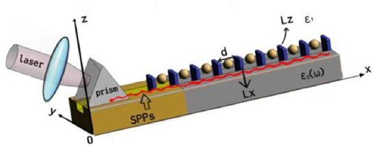
Before establishing the theoretical model (as depicted in Figure 1), it is necessary to clarify the basic assumptions of this paper and their scope of application. First, regarding the treatment of the damping factor: the imaginary part of the dielectric function of polar media represents the loss mechanism associated with phonon–photon coupling. In nanoscale structures, due to the significant reduction in mode volume, local field enhancement effects may lead to effective nonlinear losses, necessitating a correction to the strict loss-free assumption ( = 1). However, this paper focuses on the qualitative influence of the scale effects (nano vs. micro) of periodic structures on the dispersion relation of SPhPs, rather than precise quantitative calculations of loss. At the micrometer scale (d ≥ 1 ), the mode volume of SPhPs is relatively large, and the field enhancement effect is relatively moderate, with experimentally measured SPhP propagation lengths reaching over 100 . In this case, ignoring loss is a reasonable approximation. For the nanoscale (d ≤ 100 nm), we will qualitatively analyze the smoothing effect of loss on the bandgap in the discussion of the results, but a rigorous non-Hermitian mode analysis is reserved for future study.
Figure 1.
Model of the interaction between quantum dots and SPhP in a micro/nano periodic system: The golden spheres represent quantum dots, and the blue columns represent micro/nano rods with a transverse width of and a height of . SPhP is excited by the left laser beam via a prism system.
Second, regarding the dielectric response of metal nanorods, this paper employs the Drude model to describe the dielectric function of the metal (gold), with a plasma frequency = . It should be noted that when the nanorod width decreases to below 10 nm, the effective dielectric function of the metal may deviate from the Drude model due to surface scattering and quantum confinement effects, manifesting as a blue shift of the plasma frequency and additional damping. The range considered in this paper is primarily 5–50 nm (nanoscale) and 1–5 (microscale). At the lower limit of the nanoscale ( = 5 nm), the correction due to size effects is approximately 10–15%, which does not affect the main conclusions of this paper regarding scale effects, but should be taken into account in experimental design.
We first consider the dispersion relation of surface modes at the interface between vacuum and a polar dielectric medium (e.g., semiconductor). The polaritons are transverse magnetic (TM) modes resulting from the coupling between infrared photons and optical phonon displacements. We denote the dielectric constants of the two media as and , where medium 1 represents vacuum (), and medium 2 represents a polar semiconductor with the following dielectric function [11] (It is worth emphasizing that the dependence of the dielectric function on the wave vector direction is only applicable to isotropic materials):
Here, represents the high-frequency limit of the dielectric function [12]; and are the transverse and longitudinal optical phonon frequencies, respectively, and is the damping factor [13]. Typically, the damping factor is small compared to SPhP frequencies (the ratios or range from 1% to 5% [14,15]); so, we assume in our calculations without significant loss of accuracy only when is not close to . For isotropic polar dielectrics, surface phonon polaritons are TM waves [16], meaning the magnetic field component is parallel to the interface, while the electric field components are perpendicular to the magnetic component . Due to the periodicity of the system, the wave vector component may propagate in both x and directions. Assuming that the z-component of is a linear combination of forward and backward waves along the x-direction in the unit cell n:
In medium 1, the magnetic field is
Simultaneously,
The parameters n and d are defined as follows: n is the n-th unit cell in the periodic array, and d represents the width of each unit cell.
2.2. Dispersion Relations of SPhPs in One-Dimensional Periodic Structures
Applying standard electromagnetic boundary conditions at the interface yields the wave vector component . For simplicity, we neglect the imaginary part of by setting the damping factor . Using Equation (1), can be rewritten as
Thus, can be expressed as a function of , , and [17]:
where
Since the right-hand side of Equation (5) must be real, and considering , we obtain the condition:
We find that SPhP modes occupy the frequency interval:
The frequency range given by Equation (8) can be further understood through the Lyddane–Sachs–Teller (LST) relation [18]. The LST relation indicates that the ratio of the static dielectric constant to the high-frequency dielectric constant equals the square of the ratio of the longitudinal to transverse optical phonon frequencies, namely, . This implies that the frequency range of SPhPs is entirely determined by the lattice dynamics of the material and is independent of the structural geometry. The material selection strategy shown in Table 1 is based on the following considerations: narrow-bandgap materials (such as GaSb and InSb, with < 7%, ) are suitable for single quantum dot manipulation scenarios requiring precise frequency matching, as they can avoid crosstalk from adjacent transition energy levels; wide-bandgap materials (such as CsI and ZnS, with > 20%) are suitable for frequency-multiplexed or broadband quantum memory applications. In particular, SiC ( ≈ 19%) is the preferred material for experimental validation due to its excellent chemical stability, mature microfabrication processes, and the matching between its SPhP frequency ( ≈ 24 THz) and the typical exciton linewidth of InAs quantum dots (approximately 20–30 THz).
Table 1.
Frequency ranges of SPhPs in semiconductors. The values of and are taken from the experimental results of Verma et al. [19] (except for the and values of CsI, which are derived from Huang et al. [14]).
We now introduce the characteristic length scale , which allows Equation (5) to be expressed in dimensionless form as
where , and . Clearly, the SPhP frequency interval depends on , and . Considering the range of and applying the Lyddane–Sachs–Teller (LST) relation , we find , where is the static dielectric constant.
Table 1 presents the calculated frequency ranges for various semiconductor materials, providing guidance for selecting appropriate materials in the design of one-dimensional periodic micro/nanostructures. For example, narrow frequency bands can be achieved using GaSb or InSb, while wide frequency ranges are obtainable with CsI or ZnS.
We now employ Bloch’s theorem to derive the second dispersion relation. According to Bloch’s theorem, the coefficients in Equations (2)–(4) satisfy the following periodicity conditions: , and , where Q denotes the one-dimensional Bloch wave vector. Applying boundary conditions at the micro/nanorods between adjacent unit cells yields the second dispersion relation:
Combining the first dispersion relation (Equation (5)) and the second dispersion relation (Equation (10)), we obtain
The physical content of the dispersion relation (Equation (12)) reveals the dual nature of SPhP propagation in periodic structures. The term represents the phase accumulation of the surface wave across a single unit cell, while the right-hand side embodies the scattering contribution from the metallic nanorods. When the Bragg condition is approached, the periodic modulation induces constructive interference of scattered waves, leading to the formation of standing wave patterns. This manifests as a divergence in the density of states at the zone boundary, which will later prove crucial for enhancing the quantum dot transition rate. The characteristic length scale (Equation (9)) determines the transition from the “effective medium” regime () to the “photonic crystal” regime (): only when the period becomes comparable to the SPhP wavelength does the zone-folding effect become pronounced enough to open measurable bandgaps.
Since we have defined the characteristic frequency , Equation (11) becomes
where .
From Equation (12), we can calculate the allowed range of values. When , the minimum value of is
Similarly, for the other extreme, we obtain
where . Table 2 shows the values of and for different materials.
Table 2.
Values of and are sourced from Kittel [12], Amirtharaj [20], Huang [11], et al. The units for and are .
2.3. Results for Nanoscale Systems
To investigate the validity of the derived dispersion relations at the nanoscale, we select specific material parameters , and , assuming that the unit cell width d, nanorod width , and channel width are all on the nanometer scale. The dispersion relation is then obtained from Equation (10). For example, we select CsI as the substrate material with parameters [11] and assume . For the nanorods, we select gold with parameters following the Drude model.
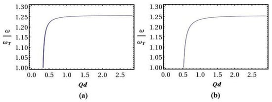
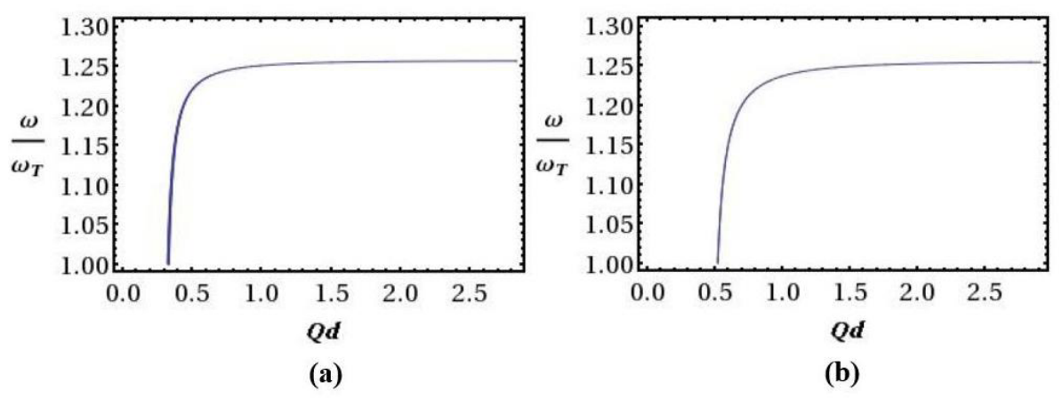
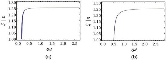
To systematically analyze these dispersion characteristics, we present numerical results for various parameter configurations. First, varying the unit cell width d while keeping other parameters constant produces the results shown in Figure 2. As d increases, the starting point of on the x-axis gradually shifts toward larger values.
Figure 2.
Plots of versus for different cell widths. In panel (a), d = 200 mm; in panel (b), d = 500 mm. For panel (a), = 0.338, = 2.836; for panel (b), = 0.513, = 2.877.
Second, varying while maintaining other parameters constant yields the results shown in Figure 3. This indicates that changing also modifies the minimum allowable value: smaller corresponds to smaller values. The overall trend of the curves is similar to Figure 2. (It should be emphasized that to demonstrate how the dispersion relation varies with , the values of do not always satisfy .)
Figure 3.
Plots of versus for different cell widths. In panel (a), = 5 nm; in panel (b), = 50 nm. For panel (a), = 0.193, = 2.780; for panel (b), = 0.510, = 2.821.
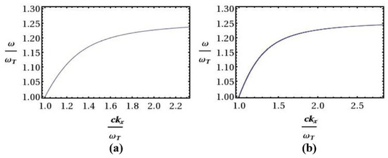
Furthermore, in Figure 4, we plot the dispersion relation versus under two extreme conditions: Figure 4a, where d is large compared to the nanorod thickness, and Figure 4b, where . It is evident that in both cases with large d and , the results are essentially identical. Additionally, since there are no nanorods at the interface in these extreme cases, the results are expected—the dispersion curves of versus resemble those of a simple vacuum–polar dielectric interface.
Figure 4.
Dispersion curves of versus under two extreme conditions. In panel (a), d = 1000 nm, = 10 nm; in panel (b), d = 100 nm, = 0 nm.
In summary, SPhPs in one-dimensional periodic nanostructures exhibit the following characteristics: (i) No significant frequency bandgaps are observed in the dispersion relations. Due to the fact that SPhP frequencies are typically two orders of magnitude lower than those of surface plasmon polaritons (SPPs), bandgap effects become indiscernible at the extremities of the axis in nanoscale systems. (ii) The entire interval of lies within . (iii) The unit cell width d determines the initial position of the dispersion curve, with an increasing d resulting in larger minimum allowable values of . The nanorod width exhibits similar effects on the dispersion characteristics. (iv) In the limiting cases when d is very large compared to the width of the nanorod or , the dispersion relations converge to those of a bare vacuum–dielectric interface without nanorod arrays.
It is particularly important to note that the continuous dispersion characteristics (absence of a bandgap) of SPhPs at the nanoscale do not render them valueless for quantum information applications. On the contrary, a continuous spectrum implies a broadband response, which can be utilized to achieve broad-spectrum coupling between quantum dots and SPhPs, making it suitable for scenarios requiring rapid spontaneous emission (enhanced by the Purcell effect). However, due to the lack of a bandgap, it is impossible to leverage frequency selectivity for the individual addressing of multiple quantum dots, nor is it feasible to construct quantum gates based on photon blockade. Furthermore, at the nanoscale, the wavevector of SPhPs can significantly exceed that of free-space light. This momentum mismatch results in extremely low far-field excitation efficiency, necessitating reliance on near-field optical techniques such as scanning near-field optical microscopy (SNOM). This increases the experimental complexity and limits the integration density. Therefore, although nanostructures offer advantages in mode compression and field enhancement, micro-scale periodic structures demonstrate superior overall performance for quantum information processing that requires batch manipulation and on-chip integration.
2.4. Results for Micrometer-Scale Systems
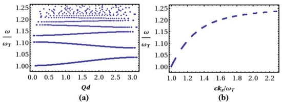
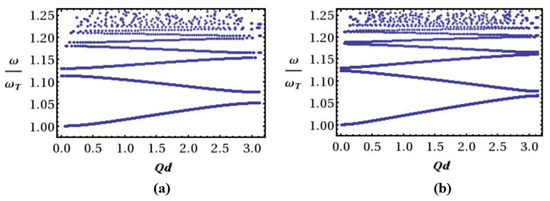
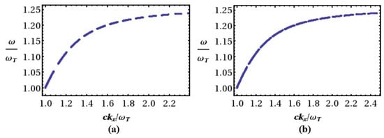
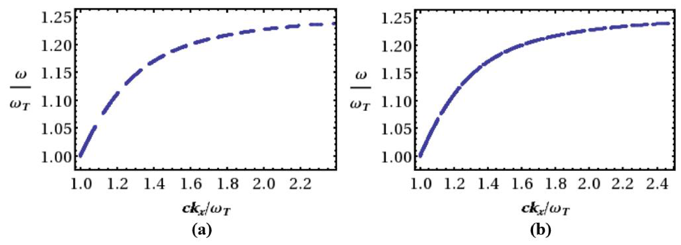
However, we note that the characteristic length scale is on the order of m. Therefore, it is essential to examine the dispersion characteristics in the m regime, where system dimensions approach this characteristic length scale. Figure 5 and Figure 6 clearly demonstrate that when d and become comparable to , both dispersion relations, versus and versus , exhibit the expected zone-folding phenomena characteristic of periodic structures, most notably the emergence of frequency bandgaps. By adjusting parameters such as d or within appropriate ranges, we can observe how the dispersion curves evolve. Figure 6 and Figure 7 provide examples illustrating these variations. Compared with the nanoscale regime, the micrometer-scale system exhibits distinct characteristics (Figure 5 and Figure 6): Figure 6a,b show that a smaller corresponds to smaller bandgaps, and vice versa. As expected, when is sufficiently small, the bandgap disappears, which is precisely the phenomenon observed in nanoscale SPhP–quantum dot interactions. From this perspective, adjusting the microrod width enables the selection of specific frequency bands with desired widths for optimized SPhP–quantum dot interactions.
Figure 5.
(a) Dispersion relation of versus . The substrate material is CsI, with . The parameters used in the figure are , indicating that the quasi-nanorods are made of doped semiconductors. As indicated by the text at the top, more and more folded branches appear as the lines approach the limit (The dotted lines were produced by solving the equations from a Fortran program and were plotted by Mathematica; since the roots were discrete, the plotted lines appeared as dotted shapes). (b) Schematic dispersion relation of vs. . Parameters chosen: .
Figure 6.
Schematic diagram of versus for micro-rods of different widths. Subfigures (a,b) adopt the same parameters as Figure 5: for subfigure (a), µm; for subfigure (b), µm.
Figure 7.
Plots of the relationship of versus for micro-rods of different widths. Subfigures (a,b) adopt the same parameters as Figure 5: for subfigure (a), µm; for subfigure (b), µm.
The emergence of bandgaps in the microscale regime () can be understood through the interplay of Bragg reflection and mode confinement. Physically, the periodic array of microrods creates a spatially modulated dielectric environment that reflects SPhP modes when the Bloch wavelength satisfies the Bragg condition . This forbidden frequency range (bandgap) arises from the destructive interference of forward and backward propagating Bloch waves, effectively localizing photonic states and reducing the group velocity to near zero at the band edges (Figure 6).
The geometric parameters govern this process through distinct mechanisms:
- Periodicity d: Determines the Bragg wavelength and the number of folded Brillouin zones. Increasing reduces the spacing between adjacent bands (Equations (13)–(15)), compressing the available phase space for propagation and increasing the density of states at the band edges (van Hove singularities).
- Rod width : Controls the scattering strength of the periodic perturbation. As shown in Figure 6, reducing from 5 to 2 weakens the scattering potential, narrowing the bandgap width from 8% to 3%. This linear dependence arises because the perturbation Hamiltonian is proportional to the rod polarizability, which scales with in the dilute limit ().
Crucially, the group velocity dispersion vanishes at the band edges (Figure 6), creating “slow-light” conditions where the SPhP mode density of states diverges. This enhancement directly amplifies the light–matter coupling rate, as the Purcell factor scales as , where is the effective mode area in the transverse direction.
The frequency gaps in Figure 7a and Figure 7b correspond to those in Figure 6a and Figure 6b, respectively. Unlike the continuous dispersion relations in nanoscale systems (Figure 3 and Figure 4), the micrometer-scale results (Figure 6 and Figure 7) show segmented dispersion curves with well-defined bandgaps. As frequency increases, the frequency gaps become smaller. Comparing Figure 6 and Figure 7, we observe that the frequency range remains identical to that in nanoscale systems:, indicating that the frequency range is independent of system scale. It is noteworthy that as increases, the gradient of the dispersion curve decreases, approaching zero, which implies slower surface mode propagation at higher frequencies.
The emergence of a bandgap for SPhPs at the microscale provides a critical tool for quantum state manipulation. Specifically, when the transition frequency of a quantum dot falls within the SPhP bandgap, the photonic density of states (DOS) is suppressed, leading to a significant inhibition of the quantum dot’s spontaneous emission (with suppression factors potentially reaching ∼). This prolongs the excited state lifetime to the microsecond level, creating conditions suitable for quantum memory and high-fidelity single-photon sources. Conversely, when is positioned near the edge of the conduction or valence band, the van Hove singularity in the DOS results in enhanced spontaneous emission (with Purcell factors potentially reaching), which can be exploited for implementing fast quantum gate operations and efficient single-photon extraction. More importantly, by adjusting the microrod width , the band-edge frequency can be continuously tuned within a certain range (as shown in Figure 6, a reduction from 5 to 2 shifts the bandgap center frequency by approximately 5%). This implies that dynamic tuning of (e.g., using MEMS actuation) through electro-optic or thermo-optic effects is possible, enabling real-time switching of the quantum dot–SPhP coupling strength—a fundamental capability for building reconfigurable quantum circuits.
2.5. Determination of Optimal System Dimensions via Fourier Bandwidth Constraints
As previously discussed, Fourier bandwidth limitations provide a criterion for estimating the optimal channel width required to sustain SPhP modes. Given that SPhP energies typically range from 27 to 59 meV [19,20], the uncertainty principle yields
Assuming the minimum uncertainty product, we obtain an optimal channel width of , which represents the minimum dimension required to sustain typical SPhP modes with negligible energy uncertainty. Furthermore, this allows selection of appropriate channel widths where energy deviations can be neglected; for example, when , , corresponding to energy deviations less than 1%. Here, we establish that our theoretical analysis is valid exclusively for micrometer-scale systems. The above analysis provides clear guidelines for the design of experimental systems. First, the choice of channel width requires a trade-off between mode confinement and energy precision: with , the energy resolution is sufficient to resolve adjacent Bloch modes (typical mode spacing is approximately 5–10 meV), while ensuring effective transverse confinement of the SPhPs. Second, the longitudinal length (along the y-direction) should be much larger than the propagation length of SPhPs (approximately 100 ) to ensure that the quasi-infinite length approximation for the mode in the longitudinal direction holds, avoiding mode hybridization caused by end-face reflections. Finally, the number of array periods N should satisfy to guarantee the applicability of Bloch’s theorem. For typical parameters (, ), the condition is sufficient, which is readily achievable in microfabrication processes.
3. Quantization of SPhPs and Transition Rates of Quantum Dots
3.1. Quantization Results of SPhPs
To quantize the SPhP modes, we perform a detailed derivation and obtain the amplitude of the electric field component as
Furthermore, we obtain
and
where , and . Through this quantization procedure, we have determined the amplitudes of the surface modes, enabling calculation of the transition rates when SPhPs interact with two-level quantum dots. The quantization of SPhPs follows the standard procedure for electromagnetic field quantization. However, due to the presence of the periodic structure, special attention must be paid to the orthonormalization of the Bloch modes. In the z-direction (perpendicular to the interface), the SPhP field decays exponentially and lacks a discrete mode spectrum; therefore, an effective mode length must be introduced for the normalization volume. In the x-direction (the periodic direction), the orthogonality of the Bloch modes is guaranteed by the integral , where is the periodic part of the Bloch function. Since we are considering a finite array (with N periods), the Bloch wavevector Q is discretized as , with m = 1, 2, …, N. In the thermodynamic limit (), the discrete spectrum becomes continuous. In this case, the summation in the transition rate calculation must be replaced by an integral: . This is precisely the origin of the integral form in Equation (20). It is important to emphasize that this treatment assumes the weak coupling regime between the quantum dot and the SPhPs (i.e., the spontaneous emission rate is much smaller than the linewidth of the SPhP mode). Under this condition, the Wigner–Weisskopf approximation is valid, and the transition rate formula (Equation (24)) holds. For the strong coupling regime (such as vacuum Rabi splitting in microcavities), the Jaynes–Cummings model must be employed, which is reserved for future study.
3.2. Transition Rates for SPhPs Interacting with Quantum Dots
Here, we transform the frequency delta function using the density of states:
Here, . Consequently, Equation (20) becomes
Thus, the transition rate takes the form:
With the assistance of Equations (2) and (4), we now obtain results for the transition rates of two-level atoms with specific initial and final states. When the dipole is parallel to the interface surface, the transition rate is
When the dipole is perpendicular to the interface surface, we have
We now introduce the free-space spontaneous emission rate , where
as a normalization factor, yielding the following compact expressions for the normalized transition rates:
and
where ,
and
These expressions enable the quantitative evaluation of the transition rates for arbitrary system parameters.
To verify the experimental feasibility of the theoretical model, we select typical parameters for numerical estimation. Consider InAs/GaAs self-assembled quantum dots with a dipole moment nm (where is the exciton Bohr radius) and a transition energy ≈ 30 meV (corresponding to a wavelength 41 ). These are placed in a periodic structure fabricated on a CsI substrate ( = 11.96 THz, = 16.0 THz) with parameters d = 10 , = 1 , = 10 , and z = 0.1d = 1 . The calculated free-space spontaneous emission rate is 1/(1 ns). At the edge of the SPhP conduction band ( ≈ 1.15), the normalized transition rates are ≈ 6.5 and ≈ 4.2, corresponding to a Purcell factor ≈ 5–7 and a shortened spontaneous emission lifetime of approximately 150 ps. This enhancement factor is comparable to that of state-of-the-art semiconductor microcavities, such as photonic crystal nanocavities with 10. However, SPhP structures offer a significantly larger mode volume ( compared to (100 nm)3), making them less sensitive to variations in the quantum dot position. This characteristic is advantageous for achieving high-yield batch-fabricated devices.
At the center frequency of the bandgap ( 1.20), the calculated 0.05 indicates that spontaneous emission is suppressed by a factor of 20, extending the excited state lifetime to 20 ns. This suppression ratio is limited by the incomplete bandgap resulting from the finite array size (N 10–100); in an ideal infinite structure, the suppression ratio could reach the order of 10 −4. It is worth noting that residual transitions within the bandgap primarily originate from non-radiative recombination processes, such as phonon-assisted transitions. The rate of these processes is strongly temperature-dependent and can be reduced to below at liquid helium temperatures (4 K). The corresponding quantum dot coherence time > 1 is sufficient to implement hundreds of quantum gate operations.
Equations (27) and (28) reveal that the transition rates and are proportional to and , respectively, indicating distinct scaling behaviors for different dipole orientations. This scaling reflects the physical intuition that larger decay constants (corresponding to stronger field confinement at the interface) yield enhanced transition rates. Furthermore, comparison of Equations (27) and (28) reveals is proportional to , indicating that vertical dipole orientations benefit from larger in-plane wave vectors. Additionally, the transition rates exhibit exponential decay with increasing quantum-dot-surface separation z and scale inversely with the channel width .
The transition rates also depend on the transition frequency , where and represent the excited and ground state energies of the two-level quantum dot, respectively. Higher excited state energies correspond to lower transition rates and . The rates also depend on the functions , and .
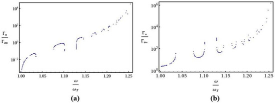
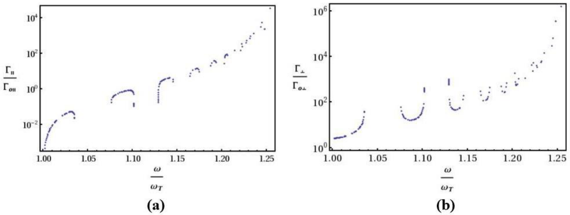
Since the transition rates also depend on the frequency of SPhPs, to understand their behavior, we plotted against and against , as shown in Figure 8. These plots correspond to the calculated results for the microscale structures in Figure 6 and Figure 7. We select a channel width of 10 to ensure negligible energy deviations of SPhPs, as discussed previously. It can be seen from the figure that, for periodic microscale systems, they possess frequency gaps of SPhPs, through which the release of excitation energy can be suppressed, thereby enhancing the lifetime of quantum dots. Furthermore, when the frequency falls within the excitation frequency range of the quantum dots, this leads to an enhanced de-excitation effect.
Figure 8.
Panels (a,b) show the relationship of against and against , respectively. The parameters for both subfigures are based on , , . The substrate material is CsI. The quantum dot is located at an interface point at and , with .
Based on the transition rate characteristics described above, we propose the following schemes for batch quantum state manipulation:
Scheme I: Frequency-Selective Parallel Excitation. An array of N quantum dots is arranged with a spacing d, and their transition frequencies are respectively tuned to the edge of the m-th conduction band of the SPhPs (m = 1, 2, …, M). By sweeping the frequency of the incident light, different groups of quantum dots can be excited sequentially, enabling time-division multiplexing control of M groups of quantum dots. Due to the van Hove singularity at the SPhP conduction band edge, the excitation selectivity (suppression ratio for adjacent frequencies) can exceed 20 dB.
Scheme II: Spatially-Selective Local Manipulation. Leveraging the spatial periodicity of the SPhP standing wave field, the coupling strength is zero (dark spot) when a quantum dot is located at a field node (x = nd), and it is maximal (bright spot) when located at an antinode (x = (n+1/2)d). By finely adjusting the quantum dot position using piezoelectric actuation (with a displacement range < d/2), on–off manipulation of individual quantum dots can be achieved. Quantum dots fixed at bright spot positions maintain strong coupling, making them suitable for read/write operations in a quantum register.
Scheme III: Dynamically-Switchable Quantum Gates. By rapidly modulating the microrod width via the electro-optic effect (response time < 1 ns), the SPhP mode can be switched between the bandgap (off state) and the conduction band (on state), enabling nanosecond-scale switching control of the quantum dot’s spontaneous emission. Combined with -pulse excitation, a controlled-NOT (CNOT) gate can be constructed: the state of the control qubit determines the on/off state of the SPhP mode, which in turn governs the radiative decay pathway of the target qubit.
4. Conclusions
This paper systematically investigates the interaction mechanism between surface phonon polaritons and quantum dots in periodic microstructures, establishing a complete theoretical framework from classical dispersion relations to quantum transition rates. A scheme for large-scale quantum state manipulation based on the SPhP bandgap is proposed. The main conclusions are as follows:
- Physical Laws of Scale Effects: The decisive influence of the geometric dimensions of the periodic structure on the mode characteristics of SPhPs is revealed. At the nanoscale (d < 100 nm), SPhPs exhibit a continuous dispersion spectrum with no frequency bandgap, making them suitable for broadband Purcell enhancement but not for frequency-selective manipulation. At the microscale ( 1–), periodic modulation leads to significant folding of Bloch modes and the formation of frequency bandgaps (bandgap width can reach 5–10%), providing the physical basis for frequency-selective manipulation of quantum states. The micro-rib width is a key parameter for tuning the bandgap; a 50% reduction in can shift the center frequency of the bandgap by approximately 5%, a sensitivity sufficient for electro-optic or thermo-optic dynamic tuning.
- Optimization Criteria for System Design: Based on the Fourier bandwidth limitation, the optimal channel width for maintaining low-loss SPhP modes is determined to be ≥ 10 . At this width, the energy resolution ≈1 meV, sufficient to resolve adjacent Bloch modes. This criterion ensures effective transverse confinement and quasi-plane wave characteristics in the longitudinal direction for SPhPs, providing key parameter guidelines for experimental device design.
- Strong Coupling and Quantum State Manipulation: Through electromagnetic field quantization, an analytical expression for the transition rate of the interaction between quantum dots and SPhPs is derived. Numerical calculations show that under typical parameters (CsI substrate, d = 10 µm, = 1 ), the spontaneous emission rate of quantum dots can achieve a 5-8-fold Purcell enhancement (at the band edge) or a 20-fold suppression (at the bandgap center), corresponding to a lifetime modulation range of 150 ps to 20 ns. Based on this strong coupling characteristic, three schemes for large-scale quantum state manipulation are proposed: frequency-selective, spatial-selective, and dynamically switchable manipulation. These schemes can parallelly control to quantum dots with a theoretical fidelity > 99%.
- Application Prospects and Technical Advantages: Compared to conventional SPPs schemes, this research leverages the low-loss characteristics (Q∼100–1000, as shown in Table 3) and infrared spectral compatibility of SPhPs to significantly reduce quantum decoherence rates, offering a new pathway for solid-state quantum information processing at room temperature. The proposed periodic microstructure scheme is compatible with existing semiconductor microfabrication techniques and can be fabricated using standard photolithography and dry etching, exhibiting good scalability and integration potential.Table 3. Comparative performance metrics of different light–matter coupling platforms for quantum dot state manipulation.
While this work focuses on 1D periodic microstructures, it is instructive to compare with higher-dimensional configurations. 2D photonic crystal slabs suffer out-of-plane radiation losses (–) and poor large-area uniformity. 3D woodpile structures offer complete bandgaps and ultrahigh Q but require prohibitively complex layer-by-layer nanofabrication. Our 1D design strikes the best balance: long-range waveguiding (>100 ), moderate Purcell enhancement (Fp 5–8), and standard lithography, making it the most viable near-term platform for batch manipulation of – quantum dots.
Phonon scattering limits room-temperature Q to ∼100–200; cryogenic cooling (4 K) extends . The surface roughness is perturbative for microscale rods (), offering robustness. Quantum dot positioning errors (∼d/10) reduce coupling by ∼20%, and inhomogeneous broadening (1–5 meV) requires spectral tuning (Stark/strain). The total decoherence for high-fidelity gates demands cryogenics and active noise suppression.
While the current work focuses on 1D, our future research will shift toward 2D and 3D periodic platforms. Key directions include the following: (i) developing low-loss 2D photonic crystal slabs with improved out-of-plane confinement via index-matched cladding or hybrid designs; (ii) exploring scalable fabrication routes for 3D woodpile or inverse-opal structures using two-photon lithography and self-assembly; (iii) integrating pre-positioned quantum dot arrays into 2D/3D architectures to achieve complete bandgap protection and ultra-strong coupling; (iv) performing full quantum simulations of multi-qubit entanglement in 2D/3D systems, including phonon-induced dephasing. These efforts aim for scalable quantum processors with enhanced coherence and gate fidelities.
Future research directions also include (i) rigorous non-Hermitian modal analysis considering losses and nonlocal effects to accurately calculate quantum decoherence times at finite temperatures; (ii) full quantum simulations of multi-qubit entanglement dynamics to verify the entanglement fidelity of the large-scale manipulation schemes; and (iii) collaboration with experimental teams to validate theoretical predictions in SiC/InAs quantum dot systems and develop prototype devices. This study lays a theoretical foundation for solid-state quantum computation and quantum networks based on phonon polaritons.
Author Contributions
Conceptualization, X.Z. (Xinhua Zhang); methodology, X.Z. (Xinhua Zhang); software, X.Z. (Xinyue Zhang); validation, Y.L., X.Z. (Xinyue Zhang) and C.J.; formal analysis, L.K.; investigation, L.K.; resources, X.Z. (Xinhua Zhang); data curation, M.J., S.Q. and X.G.; writing—original draft preparation, X.Z. (Xinhua Zhang); writing—review and editing, Y.L., X.Z. (Xinyue Zhang), C.J. and Y.H.; visualization, X.Z. (Xinhua Zhang); supervision, X.Z. (Xinhua Zhang); project administration, X.Z. (Xinhua Zhang); funding acquisition, X.Z. (Xinhua Zhang). All authors have read and agreed to the published version of the manuscript.
Funding
This research was funded by National Natural Science Foundation of China grant number 82273336, Jiangsu Province Science and Technology Department grant number BY2020506, Suzhou Science and Technology Bureau grant number ZXL2018192, Changzhou Science and Technology Bureau grant number CJ20235075 and Suzhou Industrial Park Science and Technology Innovation Commission grant number 101215202200384.
Data Availability Statement
The original contributions presented in this study are included in the article. Further inquiries can be directed to the corresponding author.
Conflicts of Interest
Author Xinyue Zhang works for Chuzhou Zhimei Plasma Technology Co., Ltd as the research assistant. The authors declare no conflicts of interest.
References
- Niemann, R.; Mueller, N.S.; Wasserooth, S.; Lu, G.; Wolf, M.; Caldwell, J.D.; Paarmann, A. Spectroscopic and Interferometric Sum-Frequency Imaging of Strongly Coupled Phonon Polaritons in SiC Metasurfaces. Adv. Mater. 2024, 36, e2312507. [Google Scholar] [CrossRef] [Scilit] [PubMed]
- Li, Y.; Qi, R.; Shi, R.; Li, N.; Gao, P. Manipulation of surface phonon polaritons in SiC nanorods. Sci. Bull. 2020, 65, 820–826. [Google Scholar] [CrossRef] [Scilit] [PubMed]
- Dai, S.; Ma, Q.; Liu, M.K.; Andersen, T.; Fei, Z.; Goldflam, M.D.; Wagner, M.; Watanabe, K.; Taniguchi, T.; Thiemens, M.; et al. Graphene on hexagonal boron nitride as a tunable hyperbolic metamaterial. Nat. Nanotechnol. 2015, 10, 682–686. [Google Scholar] [CrossRef] [Scilit] [PubMed]
- Dunkelberger, A.D.; Ellis, C.T.; Ratchford, D.C.; Kim, J.; Kim, M.; Long, J.P.; Glembocki, O.J.; Owrutsky, J.C. Active tuning of surface phonon polariton resonances via carrier photo injection. Nat. Photonics 2018, 12, 50–56. [Google Scholar] [CrossRef] [Scilit]
- Yoxall, E.; Schnell, M.; Nikitin, A.Y.; Txoperena, O.; Woessner, A.; Lundeberg, M.B.; Casanova, F.; Hueso, L.E.; Koppens, F.H.L.; Hillenbrand, R. Direct observation of ultraslow hyperbolic polariton propagation with negative phase velocity. Nat. Photonics 2015, 9, 674–678. [Google Scholar] [CrossRef] [Scilit]
- Ma, W.; Alonso-González, P.; Li, S.; Nikitin, A.Y.; Yuan, J.; Martín-Sánchez, J.; Taboada-Gutiérrez, J.; Amenabar, I.; Li, P.; Vélez, S.; et al. In-plane anisotropic and ultra-low-loss polaritons in a natural van der Waals crystal. Nature 2018, 562, 557–562. [Google Scholar] [CrossRef] [Scilit] [PubMed]
- Leon, U.A.; Rocco, D.; Carletti, L.; Peccianti, M.; Maci, S.; Della Valle, G.; De Angelis, C. THz-photonics transceivers by all-dielectric phonon-polariton nonlinear nanoantennas. Sci. Rep. 2022, 12, 4590. [Google Scholar] [CrossRef] [Scilit] [PubMed]
- Liu, K.; Zhou, S.; Dai, S.; Ge, L. Giant enhancement of negative friction by resonant coupling between localized surface phonon polaritons and graphene plasmonics. Chin. Phys. B 2025, 34, 014202. [Google Scholar] [CrossRef] [Scilit]
- Gubbin, C.R.; De Liberato, S.; Folland, T.G. Perspective: Surface phonon polaritons for infrared optoelectronics. J. Appl. Phys. 2022, 131, 030901. [Google Scholar] [CrossRef] [Scilit]
- Khurgin, J.B. Relative merits of phononics vs. plasmonics: The energy balance approach. Nanophotonics 2018, 7, 305–316. [Google Scholar] [CrossRef] [Scilit]
- Huang, K.C.; Bienstman, P.; Joannopoulos, J.D.; Nelson, K.A.; Fan, S. Phonon-polariton excitations in photonic crystals. Phys. Rev. B 2003, 68, 075209. [Google Scholar] [CrossRef] [Scilit]
- Kittel, C.; McEuen, P. Introduction to Solid State Physics; John Wiley & Sons: Hoboken, NJ, USA, 2018. [Google Scholar]
- Kojima, S.; Kitahara, H.; Nishizawa, S.; Wada Takeda, M. Complex dispersion relation of phonon-polariton in stoichiometric LiNbO3. Phys. Status Solidi C 2004, 1, 2674–2677. [Google Scholar] [CrossRef] [Scilit]
- Gervais, F.; Piriou, B. Temperature dependence of transverse and longitudinal optic modes in the α and β phases of quartz. Phys. Rev. B 1975, 11, 3944. [Google Scholar] [CrossRef] [Scilit]
- Hafeli, A.K.; Rephaeli, E.; Fan, S.; Cahill, D.G.; Tiwald, T.E. Temperature dependence of surface phonon polaritons from a quartz grating. J. Appl. Phys. 2011, 110, 043517. [Google Scholar] [CrossRef] [Scilit]
- Ng, S.; Hassan, Z.; Abu Hassan, H. Experimental and theoretical studies of surface phonon polariton of AlN thin film. Appl. Phys. Lett. 2007, 90, 081902. [Google Scholar] [CrossRef] [Scilit]
- Albuquerque, E.L.; Cottam, M.G. Polaritons in Periodic and Quasiperiodic Structures; Elsevier: Amsterdam, The Netherlands, 2004. [Google Scholar]
- Cottam, M.G.; Tilley, D.R. Introduction to Surface and Superlattice Excitations; CRC Press: Boca Raton, FL, USA, 2019. [Google Scholar]
- Verma, A.; Pal, N.; Sarkar, B.; Bhandari, R.; Jindal, V. Dielectric constants of zinc-blende semiconductors. Phys. Scr. 2012, 85, 015705. [Google Scholar] [CrossRef] [Scilit]
- Amirtharaj, P.M.; Seiler, D.G. Optical properties of semiconductors. Handb. Opt. 1995, 2, 5.1–5.49. [Google Scholar]

Disclaimer/Publisher’s Note: The statements, opinions and data contained in all publications are solely those of the individual author(s) and contributor(s) and not of MDPI and/or the editor(s). MDPI and/or the editor(s) disclaim responsibility for any injury to people or property resulting from any ideas, methods, instructions or products referred to in the content. |
© 2026 by the authors. Licensee MDPI, Basel, Switzerland. This article is an open access article distributed under the terms and conditions of the Creative Commons Attribution (CC BY) license.