


Abstract
Thin-film interference in photoresist stacks can become a significant source of uncertainty in lithographic focus metrology, particularly when high measurement stability is required. To evaluate this effect, a Fresnel-based multilayer reflection model is used to analyze the optical response of the resist stack and to guide the selection of dual-wavelength illumination. On this basis, a dual-wavelength optical triangulation system is developed for focus metrology in 350 nm lithography, with signal acquisition performed by a linear charge-coupled device (LCCD). Rather than improving precision by reducing detector pitch, the system employs a two-stage sub-pixel localization strategy in which template matching provides coarse spot localization and weighted centroid interpolation refines the final position within localized calculation windows, keeping the computational cost manageable. A covariance-based uncertainty analysis predicts a total root-mean-square uncertainty of 27.23 nm. Prototype experiments were performed on a bare silicon wafer to establish the intrinsic performance of the instrument before introducing process-dependent optical effects. Under these conditions, the system achieved a vertical resolution of 10 nm, a repeatability of 35 nm, and a stability of 13.16 nm. The additional uncertainty expected under resist-coated-wafer conditions was assessed separately through the thin-film model. These results verify the baseline capability of the proposed system and support the feasibility of the dual-wavelength strategy for focus metrology in 350 nm lithography.
1. Introduction
Photolithography does more than define circuit patterns. In integrated circuit manufacturing, it also places strict demands on process stability, production yield, and device reliability [1]. As feature sizes continue to shrink and integration density keeps increasing, the performance margin of lithography tools becomes progressively smaller. Higher imaging resolution is usually obtained by shortening the exposure wavelength or increasing the numerical aperture, but neither choice comes without cost. In both cases, the available depth of focus is reduced, and the tolerance of the exposure process to wafer height variation becomes correspondingly tighter [2,3,4,5,6,7,8,9].
This change makes focus control increasingly important in practical lithography. Once the depth of focus is compressed, even small out-of-plane deviations of the wafer can affect imaging quality and pattern transfer [10]. That is why high-precision focus metrology has become a basic requirement in modern lithography equipment. The methods used for this purpose have evolved over time, from contact-based, acoustic, and capacitive approaches to optical ones that are better suited to fast, non-contact measurement. Among these candidates, optical triangulation remains attractive because the optical layout is relatively straightforward, the response is fast, and the method is well matched to precision height sensing [11,12,13,14,15].
Although the 350 nm technology node is no longer considered state-of-the-art, it continues to be extensively used in analog and mixed-signal integrated circuits, automotive electronics, and industrial control applications owing to its process maturity and cost efficiency [16]. For lithography systems operating at this node, the DOF determined by the projection optics typically lies in the range of 0.5 μm to 1.5 μm. To ensure acceptable imaging performance, substrate height variations must therefore be limited to approximately one-fifth to one-tenth of the available DOF [17,18,19,20].
Achieving this level of precision at the 350 nm node presents several practical challenges. Conventional focus measurement techniques, including structured illumination and Moiré fringe-based methods, are often constrained by system complexity and sensitivity to environmental and illumination conditions [21,22,23,24]. Structured illumination methods rely strongly on projection contrast, which varies with surface reflectivity [21]. Likewise, Moiré-based techniques require accurate phase tracking; under non-uniform illumination, phase distortions can occur, leading to an increased computational burden and reduced suitability for high-throughput, real-time control applications [24].
Despite the progress achieved in optical focus metrology, a practical difficulty remains in 350 nm lithography: the measurement signal is not determined solely by geometric displacement but is also influenced by process-dependent optical responses from the wafer surface. In particular, photoresist films introduce thickness-sensitive interference effects that can distort the reflected signal distribution and, in turn, undermine the stability of mark localization [25]. Existing suppression strategies generally rely on spectral averaging, angular averaging, or polarization-based discrimination to reduce the sensitivity of the measurement signal to thin-film interference [26,27,28]. However, for a grazing-incidence triangulation system intended for real-time in-line use, these approaches often introduce additional complexity in optical implementation, calibration, or signal processing. At the same time, high-throughput lithography tools demand both speed and robustness, which makes heavy computational compensation unattractive in practice. What is still needed, therefore, is a focus metrology scheme that can tolerate thin-film-induced disturbance without losing the simplicity and responsiveness required for in-line use. In this context, the present work adopts a dual-wavelength strategy that introduces a limited but controllable spectral degree of freedom while remaining compatible with a compact and efficient LCCD-based triangulation architecture.
These requirements have two closely related aspects. One is process-related: the measurement should remain stable despite wafer-to-wafer variation in the optical stack. The other is structural: the system should preserve a sufficiently large measurement range to accommodate realistic focus deviations in operation. In the present work, these two demands are addressed through different parts of the design. The measurement range is provided by the LCCD-based optical triangulation architecture, whereas dual-wavelength illumination is introduced to reduce process-dependent variation in the measurement signal. On this basis, we develop a dual-wavelength optical triangulation system for focus metrology in 350 nm lithography, together with a two-stage sub-pixel localization strategy based on template matching and weighted centroid interpolation. A unified analysis framework is further established to evaluate both the residual uncertainty associated with thin-film effects and the internal uncertainty arising from signal quantization, interpolation, noise, and response non-uniformity. Experiments are carried out on a dedicated prototype using a bare silicon wafer to establish the intrinsic performance of the instrument without the added complication of photoresist-induced interference, while the uncertainty expected under resist-coated wafer conditions is assessed separately through model-based analysis.
2. System Configuration
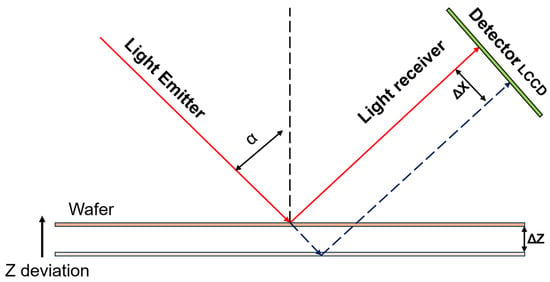
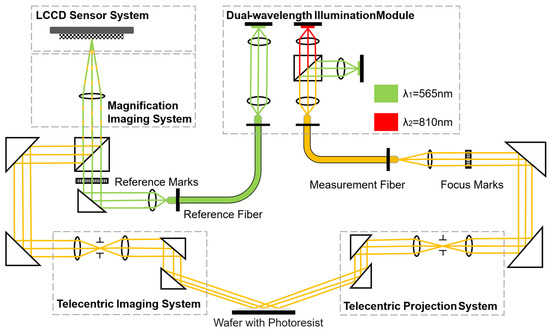
The proposed dual-wavelength optical triangulation system employs a grazing-incidence optical triangulation configuration for wafer focus measurement. The schematic diagram illustrating the principle of optical triangulation is shown in Figure 1: the wafer defocus () and the displacement of the projected mark on the LCCD () are related by the following equation:
where β is the magnification of the LCCD correction optics, and α is the incident angle of the chief ray in the wafer illumination path. In the present optical configuration, this angle is equal to the exit angle in the imaging path.
Figure 1.
The principle of optical triangulation. The black dashed line denotes the wafer surface normal, while the blue dashed line represents the reflected chief ray after wafer defocus, indicating the geometric conversion from vertical wafer displacement to lateral image displacement on the LCCD.
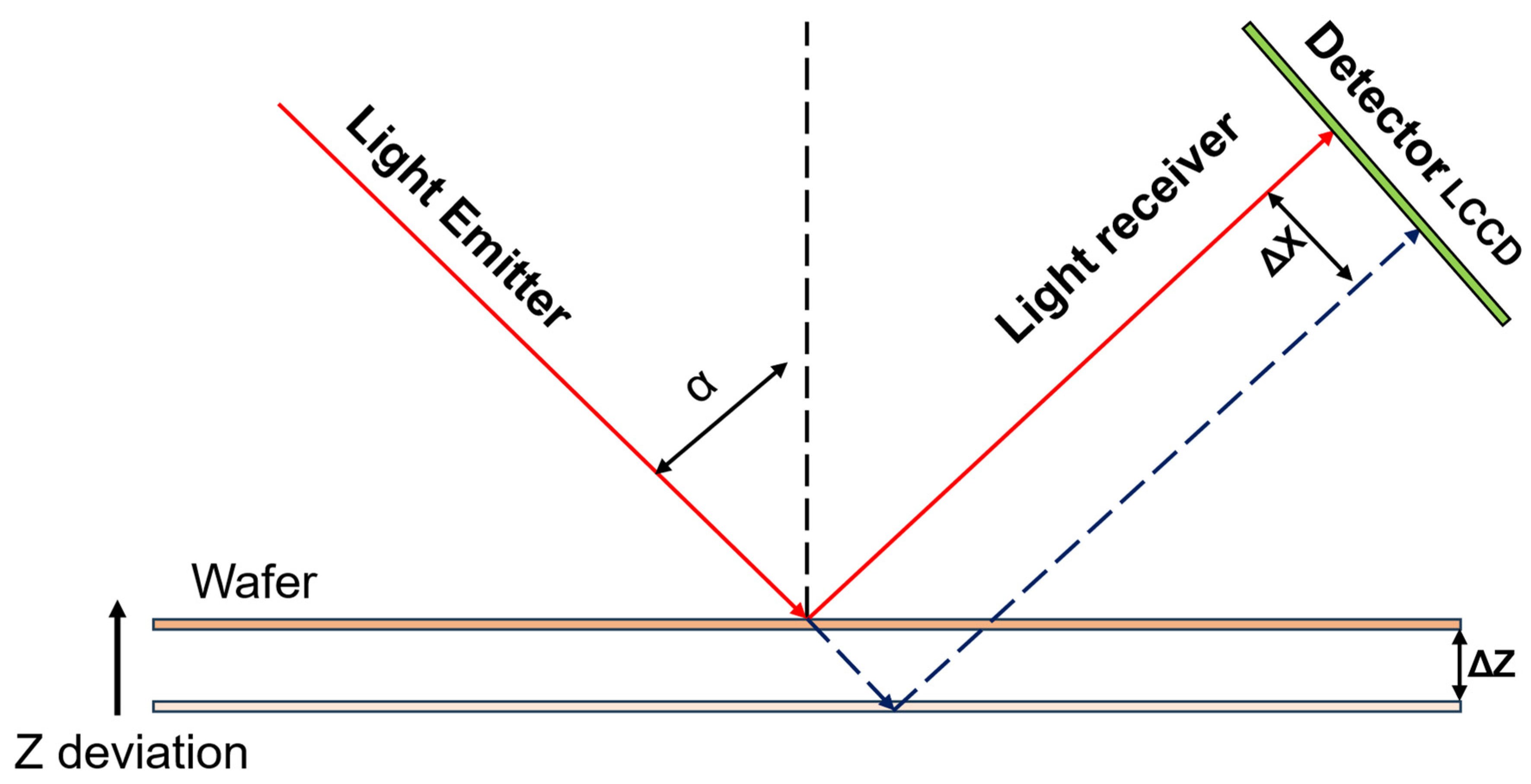
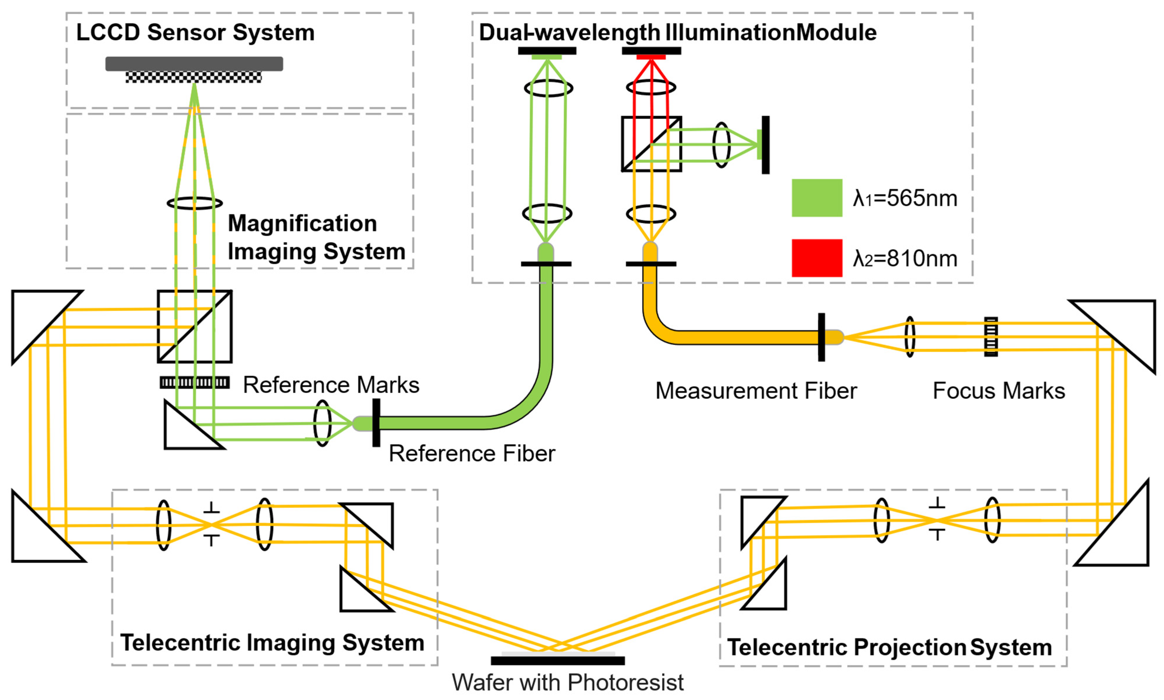
Figure 2 shows the optical arrangement of the proposed system. The optical chain begins with the dual-wavelength illumination module, which is organized around a multimode fiber. Inside this module, an 810 nm narrowband LED with a spectral bandwidth of 32 nm is merged, through a dichroic beam splitter, with a 565 nm broadband LED whose bandwidth is 103 nm, so that the emitted probe beam remains low in temporal coherence. The reference path is handled separately. A 565 nm LED source with a bandwidth of 103 nm is coupled into the reference fiber to form the reference marks, and these marks provide the baseline for real-time intensity normalization. From the measurement fiber, the probe beam enters the telecentric projection system and reaches the wafer with photoresist, where five focus marks are generated with only slight field-dependent distortion. After reflection, the signal passes through the telecentric imaging system and then the magnification imaging system, where the spot features are enlarged and the effect of residual aberration is reduced. In the final stage, the focus marks and the reference marks are simultaneously imaged onto the photosensitive surface of the LCCD sensor system for subsequent focus analysis.
Figure 2.
Schematic configuration of the proposed dual-wavelength optical triangulation system.
Taken together, the proposed optical layout separates three functions within one measurement architecture. The triangulation geometry establishes the relationship between wafer height variation and spot-centroid displacement, thereby providing the fundamental measurement range of the system. The dual-wavelength measurement path is introduced to reduce the dependence of the centroid response on stack-related optical variation, especially under resist-coated conditions. The reference marks and the five-focus-mark arrangement, together with the subsequent sub-pixel localization procedure, are intended to stabilize centroid extraction and reduce the influence of local disturbances. This functional separation also motivates the uncertainty decomposition used later in the paper, where the thin-film-related contribution and the internal localization-chain contribution are analyzed separately before being combined into a system-level uncertainty budget.
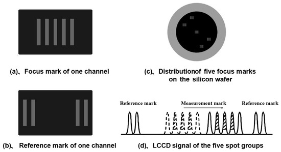
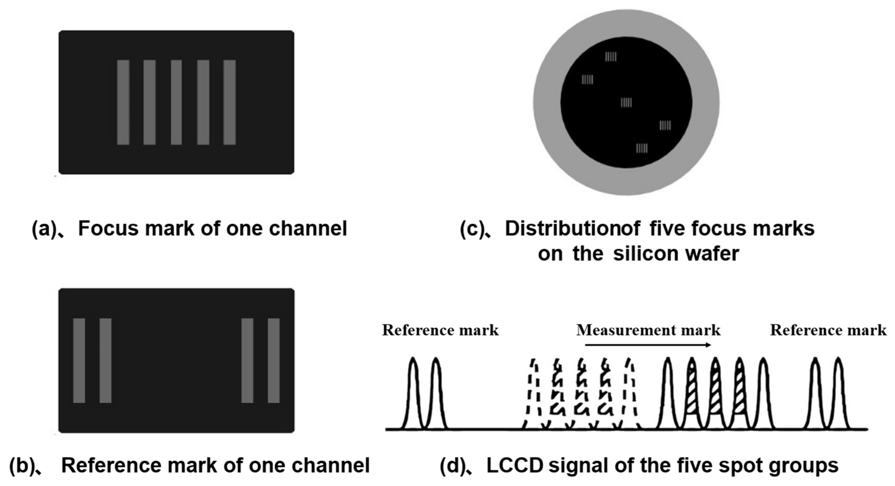
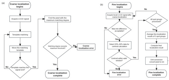
Figure 3a,b shows how the focus marks and reference marks are shaped in a single channel, while Figure 3c,d illustrates their distribution on the wafer and the corresponding LCCD signals.
Figure 3.
Focus marks and reference marks used in the proposed dual-wavelength optical triangulation system, together with their distribution on the wafer and the corresponding LCCD signals. (a) Focus mark layout of one measurement channel. (b) Reference mark layout of one measurement channel. (c) Layout of five independent focus marks on the silicon wafer surface. (d) LCCD signals corresponding to the focus marks and reference marks.
3. Principle
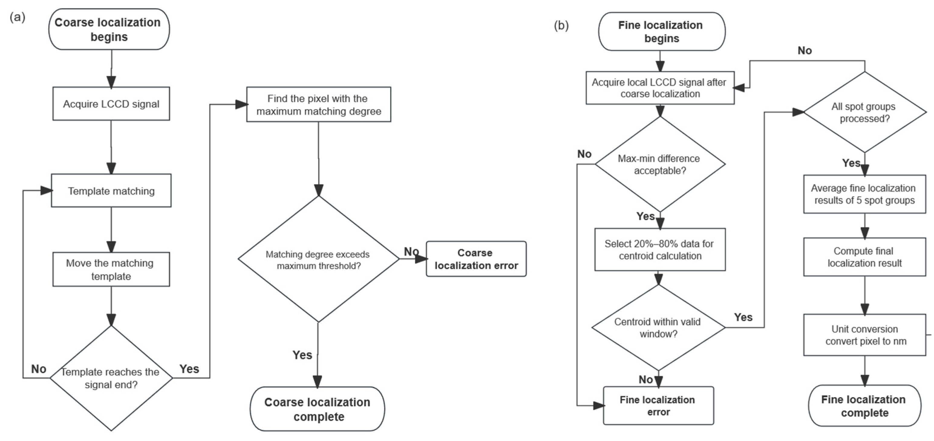
In the proposed system, localization accuracy and computational efficiency must be maintained simultaneously. A direct centroid calculation over the full LCCD signal is simple, but it is more vulnerable to background fluctuations, local interference, and spurious responses outside the effective spot region. For this reason, centroid estimation is not performed in a single global step. Instead, a two-stage sub-pixel strategy is adopted. Template matching is first used to identify the approximate position of each spot and to define a stable local calculation region. Fine localization is then performed only within this restricted window by combining linear interpolation with weighted centroid evaluation. In this way, the algorithm preserves robustness in the coarse stage while retaining sub-pixel sensitivity in the fine stage. The flowcharts of the proposed two-stage sub-pixel localization algorithm are shown in Figure 4.
Figure 4.
Flowcharts of the proposed two-stage sub-pixel localization algorithm. (a) Coarse localization based on template matching. (b) Fine localization based on signal screening, centroid calculation, multi-group averaging, and unit conversion.
3.1. Template Matching Coarse Localization Algorithm
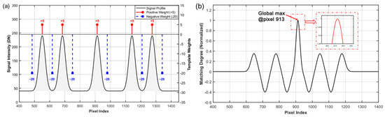
In the coarse localization stage, the spot position is found by template matching instead of direct centroid evaluation over the entire signal range. The template follows the known geometric relation between the central spot and its four neighboring peaks. Each expected peak position is assigned a weight of +5, whereas several nearby background positions are assigned −20 so that the target pattern is emphasized and spurious responses are suppressed. The use of a stronger negative weight is mainly a coarse-search consideration. At this stage, an incorrect match caused by a local background peak would shift the subsequent calculation window, while moderate intensity variation at the expected peak positions has a much smaller influence once the correct local region has been selected. Therefore, the selected weights are used to increase the contrast between the known five-peak pattern and nearby background fluctuations, rather than to determine the final sub-pixel position directly. Figure 5a shows how these positive and negative weights are arranged.
Figure 5.
Principle and validation of the template matching coarse localization algorithm. (a) Schematic diagram of the template matching weights and their positional relationships. (b) Matching degree curve of the template matching coarse localization method.
The matching score is calculated from the weighted sum of the measured signal values at seven predefined positions. As the template slides along the signal sequence with a step of one pixel, one score is produced at every candidate location. The pixel associated with the largest score is taken as the coarse localization result. For the ideal example shown in Figure 5a, this maximum occurs at pixel 913, where the template is aligned with the central peak. The full matching-score curve is given in Figure 5b.
3.2. Linear Interpolation Weighted Centroid Localization Algorithm
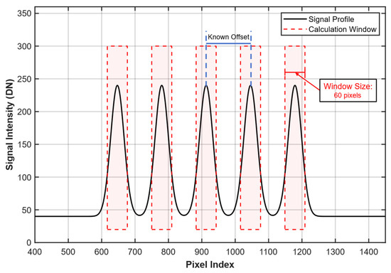
The coarse localization results anchor the definition of discrete calculation windows for the five light spots. The algorithm aligns the central window directly with the coarse coordinate while known design offsets dictate the center positions of the four peripheral windows. As Figure 6 illustrates, each calculation window spans a symmetric width of 60 pixels to ensure full coverage of the spot profile. Because both interpolation and centroid calculation are performed after coarse localization, the computation is restricted to these selected local windows rather than the full LCCD signal. This local-window implementation keeps the amount of processed data limited before the final centroid evaluation.
Figure 6.
The calculation window range and center positions for fine localization.
Within each window, linear interpolation is applied to increase the effective sampling density and to reduce the discretization effect associated with the original pixel pitch. The interpolated signal is then screened before centroid calculation. Only the data points lying between 20% and 80% of the local signal span are retained. This selection is intended to suppress the low-intensity tail, which is more vulnerable to noise and background fluctuation, while also reducing excessive sensitivity to the local peak region. The retained samples are then used in the grayscale-weighted centroid calculation defined as:
where, represents the pixel coordinates and represents the response value corresponding to pixel coordinates .
The final localization result is obtained by combining the coarse coordinate with the relative centroid position within the fine-localization window, and the five spot groups are then averaged to form the output of the measurement channel. At this stage, however, the problem is only partially solved. The localization method defines how the spot position is extracted, but the practical precision of the system is determined by how this extracted position responds to real optical and detector-side disturbances. In the present system, these disturbances arise from two main sources: process-dependent signal variation caused by thin-film interference on the wafer surface, and internal uncertainty introduced by the LCCD detection and localization chain. The next section therefore turns from signal extraction to uncertainty formation and evaluates how these factors propagate into the final measurement precision.
4. Simulation
Based on the localization framework established in Section 3, the next step is to examine the factors that determine the actual measurement precision of the proposed system. In the present work, these factors are considered from two sides. One arises from the optical response of the wafer stack, where thin-film interference changes the reflected signal and introduces additional equivalent height fluctuations. The other arises from the LCCD signal-processing chain, where quantization, interpolation, noise, and response non-uniformity can further affect the stability of localization. Seen in this way, the purpose of the simulation is not simply to reproduce the optical signal itself, but to clarify how uncertainty develops along the full measurement path, from signal formation to centroid estimation. This also allows the main disturbance sources to be discussed within a unified framework, rather than as several disconnected effects. Among the external contributions, thin-film interference is treated as the dominant one in the present study, and its behavior under dual-wavelength illumination is quantified through optical simulation. In parallel, the internal uncertainty sources associated with the detector and the localization procedure are evaluated to determine how much they contribute to the final uncertainty. The two parts are then brought together into a single uncertainty budget, which is used to estimate the achievable precision of the system.
4.1. Modeling of Thin-Film-Induced Centroid Fluctuation Under Dual-Wavelength Illumination
We begin with the process-dependent side of the problem, namely the fluctuation introduced by thin-film interference in the photoresist stack. The purpose here is not simply to describe the multilayer optical response itself, but to clarify how strongly that response enters the focus signal and how much of the resulting disturbance can be suppressed when dual-wavelength illumination is applied. For this reason, the analysis follows the optical behavior of the stack through to its influence on the equivalent measurement output, so that the thin-film-related contribution can be carried forward into the later precision evaluation.
To keep the simulation close to the actual illumination condition of the tool, the probe is not treated as a single plane wave. Instead, the wafer is illuminated by a spread of oblique plane-wave components distributed within a 3° cone around the nominal 81.5° grazing incidence. In the simulation, the nominal grazing angle is taken from the designed chief-ray geometry, while the 3° cone approximates the angular spread of the illumination bundle. The spectral samples are distributed over the LED bandwidths used in the prototype, and the reflected intensity is then averaged over both angle and wavelength. This matters because the air–photoresist–silicon stack does not respond identically at every angle. The complex Fresnel response varies across the cone, and that variation reshapes the effective pupil weighting and ultimately changes the spot profile formed on the LCCD. In the model, the multilayer Fresnel response is evaluated for each sampled wavelength within the LED bandwidth and for each angular component. The reflected field is then propagated through a pupil-limited telecentric imaging stage, and the resulting intensity distributions are averaged over angle and spectrum. In this way, the simulation gives a forward prediction of the thickness-dependent centroid variation under illumination conditions consistent with those of the prototype. The key simulation parameters are summarized in Table 1.
Table 1.
Key parameters used in the dual-wavelength thin-film interference simulation.
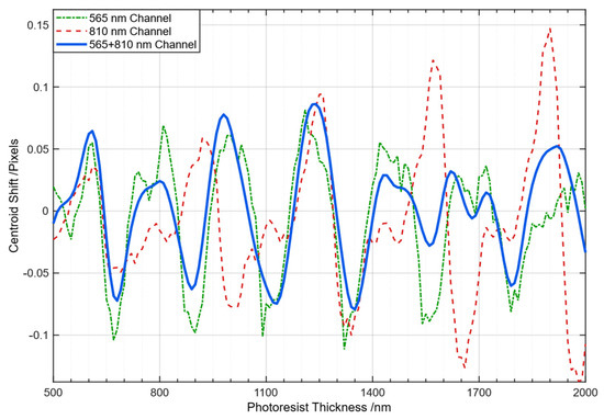
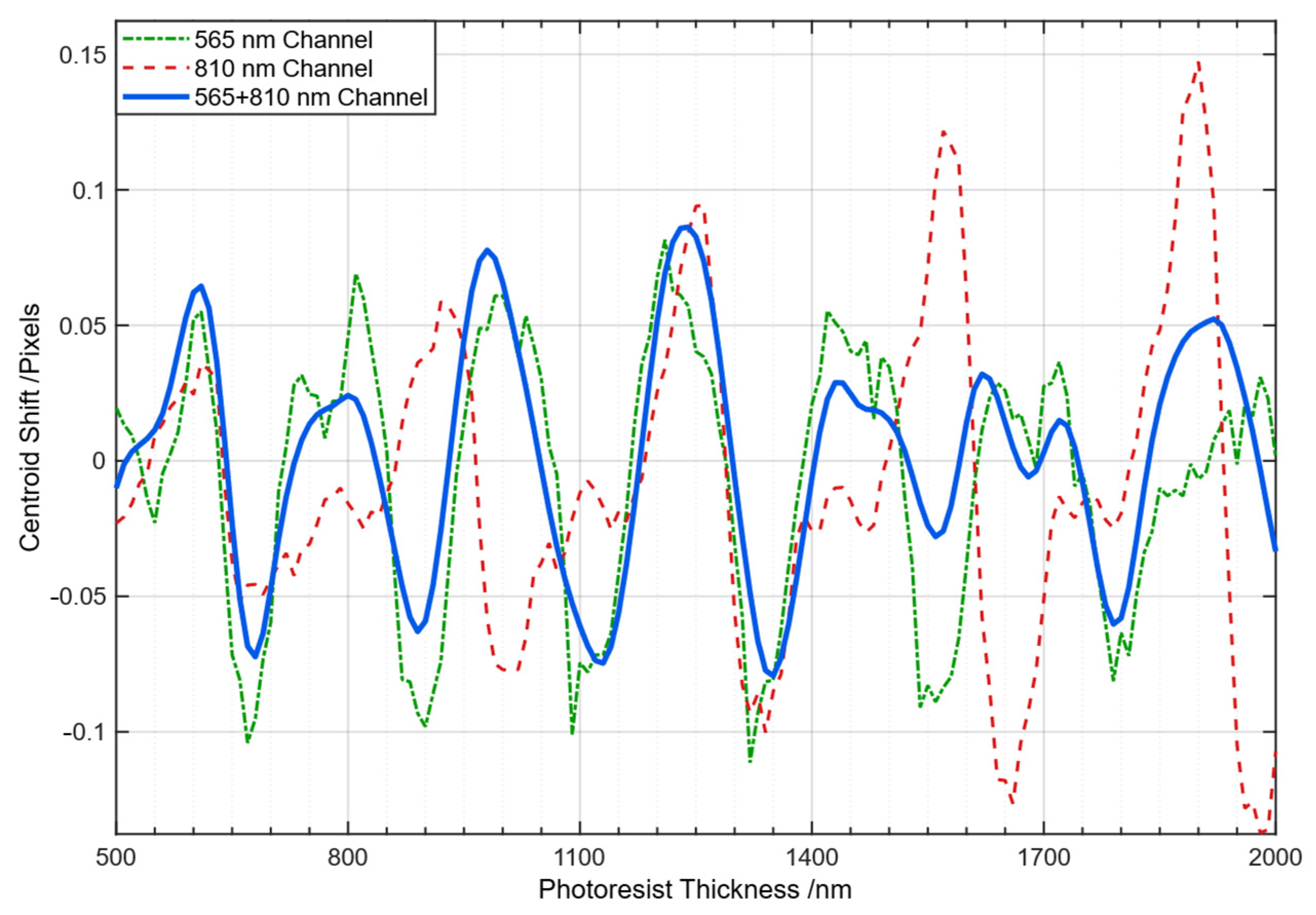
Figure 7 illustrates the simulated centroid shift as a function of photoresist thickness under grazing-incidence illumination at 81.5°. The analysis includes a 565 nm LED with a bandwidth of 103 nm, an 810 nm LED with a bandwidth of 30 nm, and their combined dual-wavelength superposition. With the angular and spectral averaging conditions defined above, these curves represent the predicted thickness-dependent centroid response of the prototype under single- and dual-wavelength operation.
Figure 7.
Centroid shift as a function of photoresist thickness under single and dual-wavelength oblique illumination.
Table 2 takes the centroid-fluctuation curves in Figure 7 and turns them into a number that is easier to interpret for real process conditions. Instead of treating the whole 500–2000 nm sweep as equally likely, we evaluate the centroid fluctuation around a typical i-line operating point by placing a Gaussian thickness window at 1.0 μm, which represents a nominal target thickness with finite within-wafer variation. In that window, the 810 nm narrowband case still shows a clear thickness-driven oscillation, and the resulting RMS centroid fluctuation is 0.0371 pixels, implying that thin-film effects can become a practical accuracy limit. With dual-wavelength illumination, the thickness sensitivity is noticeably softened because the two bands do not reinforce the same modulation. The centroid fluctuation RMS becomes 0.0274 pixels, giving a suppression factor of 1.35. Under our system magnification and triangulation geometry, this corresponds to an equivalent vertical focusing uncertainty of about 13.87 nm.
Table 2.
Model-based RMS centroid fluctuation and equivalent height uncertainty for different illumination schemes within the nominal 1.0 μm photoresist-thickness window.
It is worth noting that, within the nominal thickness window centered at 1.0 μm, the broadband 565 nm channel gives the lowest RMS value among the three cases. This does not contradict the use of the dual-wavelength design, because the selected window represents only one nominal coated-wafer condition. In practice, the resist stack is not fixed from wafer to wafer or from lot to lot. The nominal thickness may shift, and small changes in the optical properties of the resist or underlying layer can move a single-wavelength response away from its relatively stable region. The 810 nm channel is therefore retained to provide a complementary spectral response, rather than simply to minimize the RMS value at the 1.0 μm operating point.
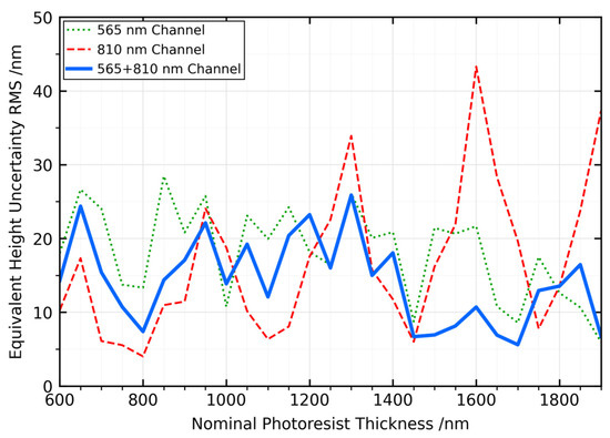
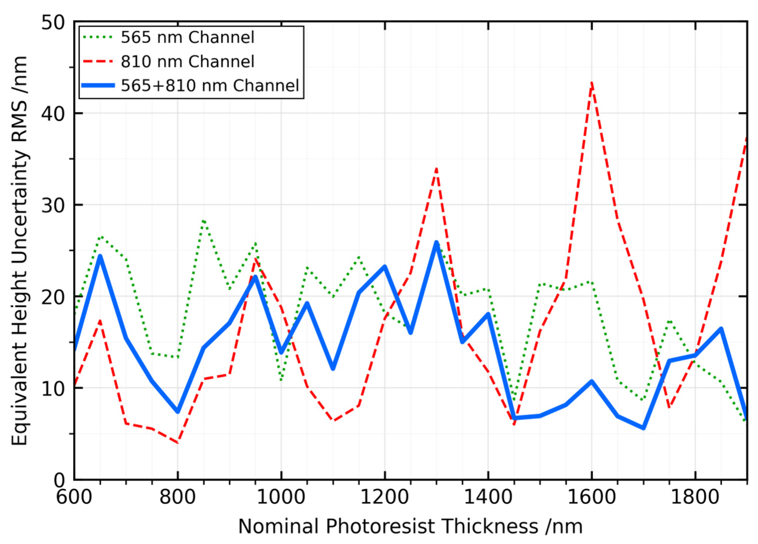
To check whether this interpretation still holds when the nominal process condition changes, a sensitivity analysis was performed by shifting the center of the Gaussian photoresist-thickness window from 0.6 μm to 1.9 μm. The standard deviation of the thickness window was kept at 30 nm, and the angular and spectral averaging conditions were kept the same as those used in the thin-film simulation above. For each nominal thickness, the centroid fluctuation was recalculated for the 565 nm, 810 nm, and dual-wavelength cases and then converted into equivalent height uncertainty. The results are shown in Figure 8.
Figure 8.
Sensitivity of equivalent height uncertainty to nominal photoresist thickness under different illumination schemes.
Figure 8 shows that the single-wavelength responses change noticeably as the nominal thickness window is shifted. This is expected, since each wavelength samples a different part of the thickness-dependent Fresnel response of the photoresist stack. Over the scanned nominal-thickness range, the mean equivalent height uncertainty is 18.11 nm for 565 nm, 16.75 nm for 810 nm, and 14.22 nm for the dual-wavelength case. The variation across the scanned thickness centers is also smaller in the dual-wavelength case, with a standard deviation of 5.84 nm, compared with 6.25 nm for 565 nm and 10.19 nm for 810 nm. In addition, the maximum RMS value of the dual-wavelength case is 25.87 nm, which is lower than that of the 565 nm and 810 nm cases.
These results do not mean that the dual-wavelength configuration yields the lowest RMS value at every individual nominal thickness. Rather, they show that the combined 565/810 nm response is less tied to the stable region of a single wavelength. This is the reason the dual-wavelength scheme is treated here as a robustness-oriented design for coated-wafer focus metrology, instead of as a best-case optimization at one selected photoresist thickness. It should also be noted that this sensitivity analysis remains model-based and does not replace direct coated-wafer validation. Its purpose is to test the robustness of the thin-film model under representative process variations and to provide a more complete basis for the thin-film-related uncertainty term used later in the uncertainty budget.
4.2. Analysis of Internal System Uncertainty and Theoretical Noise Floor
After considering the optical contribution, the analysis turns to the internal uncertainty introduced along the localization chain. In this part, attention is focused on the factors that affect centroid estimation after the signal has been recorded by the LCCD. To keep the influence of each source clear, deterministic factors such as quantization depth and interpolation settings are first examined separately, and stochastic effects, including noise and response non-uniformity, are then introduced under more realistic operating conditions. This arrangement makes it easier to see how hardware-related limitations and algorithmic parameters shape the localization accuracy before they are combined into the full measurement uncertainty.
Quantization characteristics of the acquisition hardware determine the fundamental signal fidelity. The selected bit depth defines the resolution of the digitized LCCD signal and introduces an inherent quantization error through discretization. This error establishes a lower bound for centroid accuracy, rendering bit depth a critical parameter in suppressing analog-to-digital conversion noise. For an N-bit quantizer with input range , the quantization step size is given by
The associated root mean square quantization error follows the relationship:
Intensity perturbations propagate through the grayscale-based weighted centroid algorithm to induce a spatial shift . This perturbation follows a first-order approximation:
Treating the quantization noise as independent and identically distributed across the pixel array produces the following variance for the centroid error:
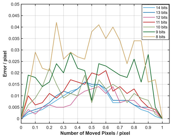
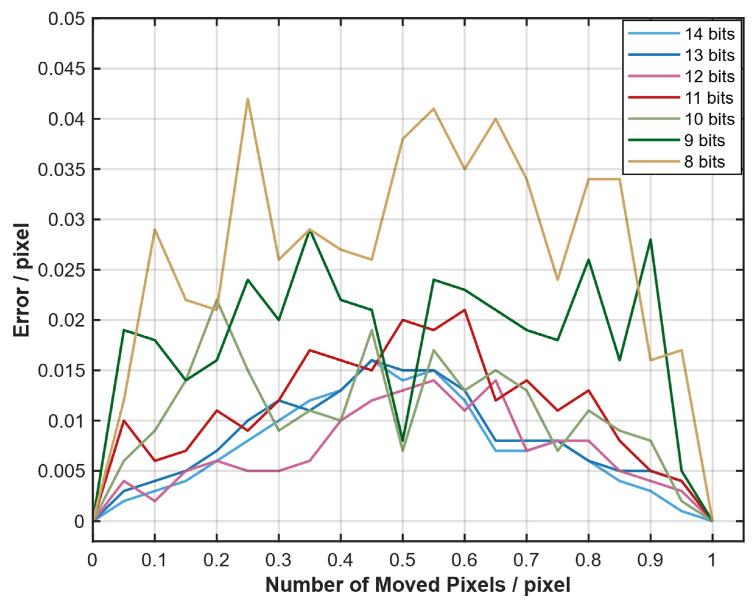
This analytical framework establishes a direct link between the quantization bit depth N and the achievable centroid precision. Figure 9 illustrates the absolute mean errors in the centroid positions of five light spots for an ideal signal characterized by 100× interpolation and the absence of noise. The results demonstrate that for bit depths ranging from 10 to 12 bits, the average error remains within 0.01 pixels.
Figure 9.
Dependence of ideal spot localization error on LCCD quantization bit depth.
Delineation of hardware quantization limits shifts the analytical focus toward algorithmic compensation. The simulation framework fixes the LCCD bit depth at 8-bit and 10-bit levels to isolate software-driven refinements from hardware bottlenecks. A parameter sweep subsequently varies the interpolation factor from 10 to 100 times to evaluate the precision recovery achieved through computational subdivision.
Interpolation effectively reduces the sampling pitch from p to p/M where M denotes the interpolation factor. This physical reduction compels the centroid localization precision to scale according to the following relationship:
where is the total photon count contributing to the spot intensity. In the presence of quantization, the centroid uncertainty variance can be expressed as the sum of interpolation-limited and quantization-limited contributions:
where is the RMS quantization noise defined by , and characterizes the interpolation error floor.
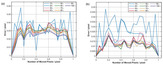
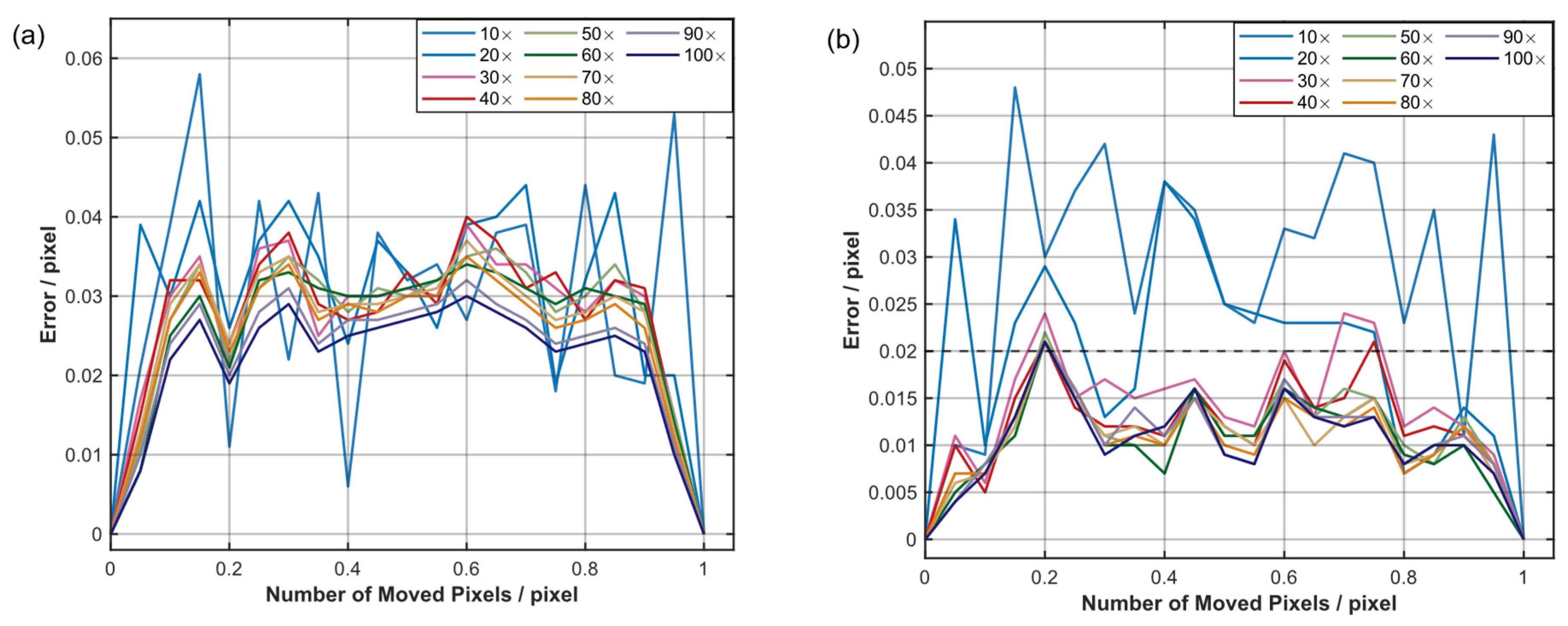
These relations show that increasing the interpolation factor M reduces the discretization error by approximately 1/M, thereby improving centroid accuracy, but the ultimate performance is jointly constrained by the quantization precision and photon shot noise. Figure 10a,b illustrates the absolute mean localization errors of the centroids for five light spots under different interpolation factors and displacements, using 8-bit and 10-bit quantization with no noise. The results indicate that for interpolation factors ranging from 50× to 100×, a 10-bit signal achieves an average localization error within 0.02 pixels. Since interpolation is performed only within the selected 60-pixel local windows, the 100× factor mainly increases the local subdivision density for centroid refinement rather than the computational load of the full localization chain. In the current implementation, one complete five-spot localization process with 100× interpolation can be completed within 1 ms. Thus, 100× is used as a conservative setting in the uncertainty evaluation, while a lower factor within the 50×–100× range may be selected when a stricter real-time margin is required.
Figure 10.
Simulated mean localization error under noise-free conditions for different interpolation factors. (a) Localization error versus interpolation factor at 8-bit quantization. (b) Localization error versus interpolation factor at 10-bit quantization.
Optimization of deterministic parameters redirects the investigation toward the stochastic noise inherent in LCCD signals. These random fluctuations in the pixel response set the ultimate precision limit for centroiding operations. The signal-to-noise ratio (SNR) provides the primary quantitative metric to characterize the magnitude of these stochastic perturbations. For signal power and noise power , the SNR follows the relationship:
The signal-to-noise Ratio (SNR) dictates the stability of the intensity distribution before the localization algorithm initiates processing and directly influences the centroid calculation. With denoting the additive noise at each pixel, the noisy centroid can be written as:
Linearizing this expression for small noise perturbations yields an approximation for the centroid deviation
Zero-mean independent noise with a variance of gives the following noise-induced centroid variance:
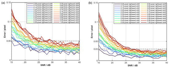
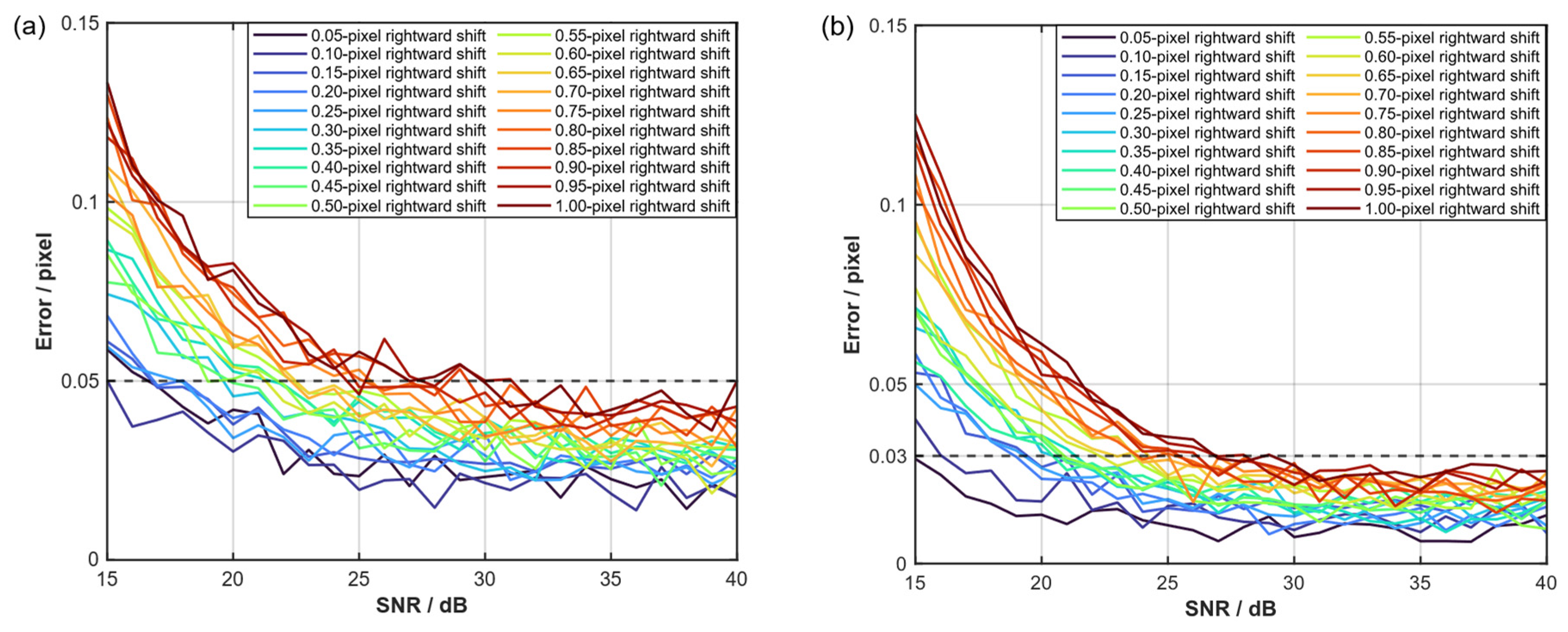
This expression explicitly links centroid precision to the noise variance and consequently to the SNR. As the SNR increases, the noise variance decreases, thereby enhancing the centroid accuracy. Figure 11a,b presents the absolute mean errors for five light spots simulated using an ideal signal employing 100× interpolation. The analysis covers various signal-to-noise ratios for both 8-bit and 10-bit quantization. Results indicate that when the SNR exceeds 30 dB, the average error for a 10-bit signal remains below 0.03 pixels.
Figure 11.
Effect of signal-to-noise ratio on centroid localization error with 100× interpolation. (a) Localization error as a function of signal-to-noise ratio at 8-bit quantization. (b) Localization error as a function of signal-to-noise ratio at 10-bit quantization.
In addition to signal noise, signal-response non-uniformity in the detected spot profile also affects centroid accuracy. In this work, this term describes relative amplitude modulation of the detected signal caused by local reflectivity variation, detector-response non-uniformity, and illumination non-uniformity, rather than only pixel-to-pixel response variation in the LCCD. To mathematically describe this influence, the pixel response is defined as:
where represents the relative non-uniformity factor, typically bounded as . Substituting into the centroid formula,
and linearizing for small , the centroid error can be approximated by
Assuming the non-uniformity is random with variance , the corresponding centroid uncertainty variance is
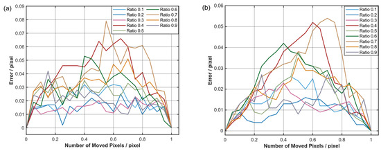
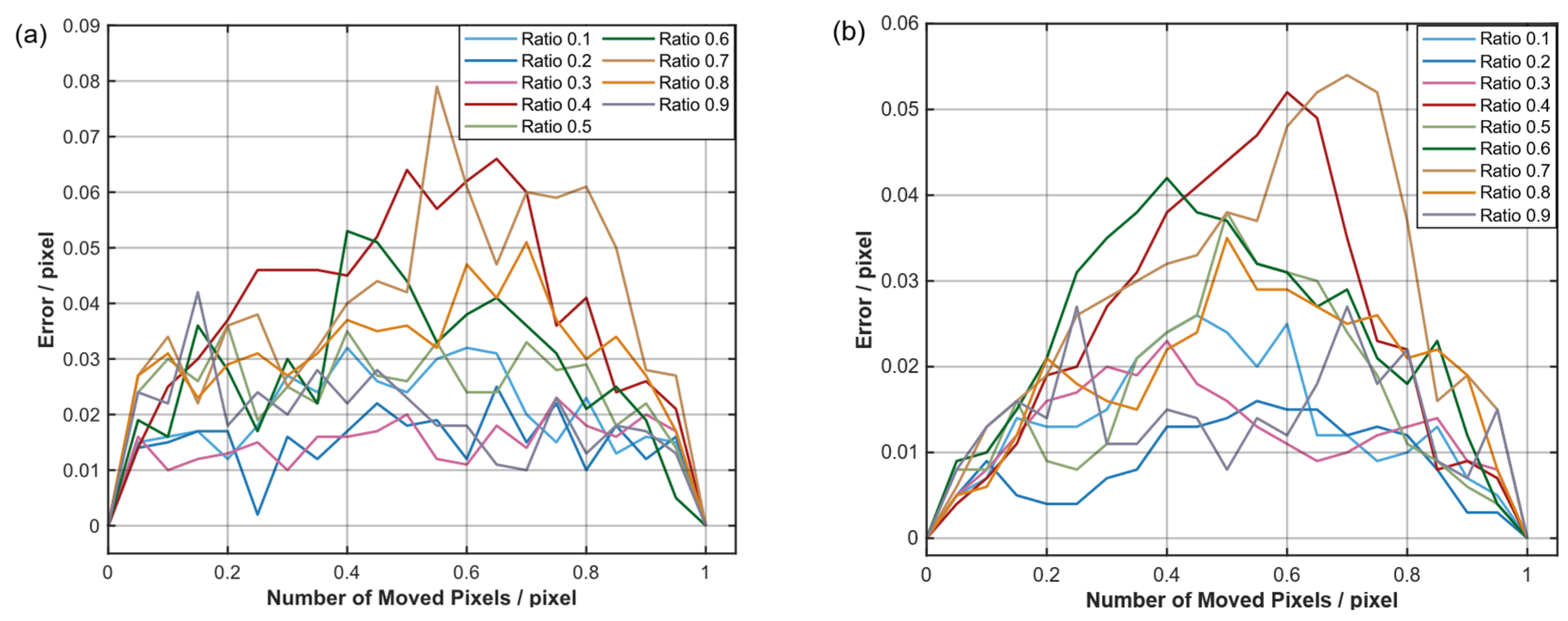
This relationship indicates that centroid precision degrades as response non-uniformity increases. However, the error is effectively constrained by sufficient quantization depth and signal strength. Figure 12a,b illustrates the absolute mean errors of the five light spots under different signal-response non-uniformity ratios. This assessment employs an ideal signal configuration featuring 100× interpolation and no added noise, so that the non-uniformity-induced localization contribution can be isolated from other stochastic perturbations. The results show that, under 10-bit quantization, the average localization error remains within 0.03 pixels.
Figure 12.
Effect of response non-uniformity on centroid localization error. (a) Localization error of an ideal spot versus non-uniformity ratio at 8-bit quantization. (b) Localization error of an ideal spot versus non-uniformity ratio at 10-bit quantization.
The synthesis of quantization, interpolation, noise, and non-uniformity translates individual uncertainty contributions into a comprehensive estimate of total system uncertainty. This integration establishes a unified covariance framework to characterize the collective impact of these factors on centroid stability rather than treating them as isolated variables. By mapping each physical and algorithmic disturbance to a common covariance domain, this system-level approach identifies the dominant contributors to the overall focus budget and predicts the representative internal uncertainty under the adopted operating condition.
Let the primary uncertainty sources—quantization (), interpolation (), noise (), and non-uniformity ()—be represented as an uncertainty-source vector
Assuming the centroid displacement can be expressed as a differentiable function of these perturbations, a first-order Taylor expansion yields
where is the Jacobian sensitivity vector, defined as . Here, each element represents the sensitivity coefficient describing how a specific uncertainty source linearly propagates to the total centroid shift.
The covariance matrix of the uncertainty sources is defined as
where denotes the covariance matrix of the uncertainty-source vector and represents the covariance between the and uncertainty sources. Then, according to first-order uncertainty propagation, the variance of the output centroid displacement is given by:
For the present uncertainty estimate, the RSS form is used as a first-order approximation of the internal centroid uncertainty. This treatment is reasonable here because the four terms mainly enter the localization chain through different routes: quantization through digital sampling, interpolation through sub-pixel resampling, signal noise through random intensity fluctuations, and response non-uniformity through fixed or slowly varying amplitude differences in the detected spot profile. Under the adopted operating condition, the cross-covariance terms which represent possible coupling among these uncertainty sources, are assumed to be smaller than the dominant variance terms. Equation (20) can therefore be reduced to the following root-sum-square (RSS) form:
The individual error curves discussed above show how each factor affects centroid localization, but they do not by themselves define a single working point for the full internal uncertainty budget. For that reason, the representative operating condition adopted in the present study, together with the corresponding uncertainty terms used in the RSS calculation, is summarized in Table 3. The adopted noise level is supported by a baseline SNR check performed under stable detector-temperature conditions. This baseline SNR check was performed using the reference-mark signals recorded by the LCCD. Using the signal amplitude in the effective half-peak regions and the local standard deviation as the noise estimate, the measured SNR values were 207.75–258.56 on a linear scale, or approximately 46.35–48.25 dB. Thus, the 30 dB SNR used in the following calculation is a conservative operating level rather than a best-case assumption. The signal-response non-uniformity ratio is treated separately in the present uncertainty estimate. This parameter describes the relative amplitude modulation of the detected spot profile, including the combined influence of local reflectivity variation, detector-response non-uniformity, and illumination non-uniformity. It should therefore not be interpreted as a direct flat-field PRNU specification of the LCCD alone. The selected value of 0.4 corresponds to a moderate-to-strong non-uniform signal condition within the tested range and is used as a representative sensitivity level for the internal uncertainty budget.
Table 3.
Adopted operating conditions and representative internal uncertainty terms used in the RSS-based internal uncertainty estimate.
Using the representative terms listed in Table 3, the standard deviations of the individual uncertainty sources are taken as approximately . These values are selected as representative estimates from the simulation envelopes shown in Figure 9, Figure 10, Figure 11 and Figure 12 under the adopted operating condition. Substituting these values into Equation (21) yields a total centroid uncertainty on the LCCD image plane of approximately .
The image-plane centroid uncertainty can then be converted into the corresponding wafer-height uncertainty through the optical triangulation geometry. Given the optical magnification and the LCCD sensor pixel size the geometric conversion factor is obtained from the optical triangulation relation as Consequently, the equivalent wafer height uncertainty is calculated as:
This theoretical internal uncertainty falls well within the permissible range, confirming that the system’s hardware and algorithmic configuration are sufficient for nanometer-level focus control.
4.3. Comprehensive Uncertainty Budgeting and System Performance Prediction
With the external optical variation and the internal localization uncertainty clarified separately, the next step is to bring them together in a single uncertainty model. In the present work, the uncertainty sources are grouped into two categories. The first is the thin-film-related residual, which comes from the wavelength-dependent optical response of the photoresist stack and represents the remaining equivalent height uncertainty after dual-wavelength suppression. The second is the internal detection uncertainty associated with signal quantization, interpolation, noise, and response non-uniformity in the LCCD-based localization chain. Since these two mechanisms act in different domains, they are treated here as statistically independent. On this basis, the total system uncertainty, , is estimated by the root-sum-square of the individual components:
where denotes the thin-film-related residual and denotes the internal detection uncertainty.
Using the representative uncertainty terms in the above model, we estimate an RMS uncertainty of 13.87 nm for the dual-wavelength residual, evaluated around a nominal 1.0 µm photoresist thickness under the assumed process window. The LCCD detection and localization chain contributes an internal uncertainty of 23.43 nm. The synthesized total system uncertainty is calculated as follows:
What matters here is that these two terms do not describe the same kind of limitation. The thin-film-related residual is an external and process-dependent contribution that becomes relevant under resist-coated-wafer conditions. The detection uncertainty, by contrast, is intrinsic to the instrument itself and remains present even when photoresist-induced interference is absent. In this sense, the present uncertainty budget is more than a single combined number, because it also shows how the dominant limitation changes with the measurement conditions.
For bare silicon wafer conditions, the main constraint arises from the internal detection and localization chain. Once resist-coated wafers are considered, the remaining thin-film-related residual becomes an additional term that defines the practical precision boundary. Under the current design, the predicted comprehensive uncertainty remains below 30 nm RMS, which suggests that the proposed dual-wavelength strategy is a technically reasonable route toward high-precision focus metrology in 350 nm lithography.
5. Baseline Experimental Validation and Discussion
To evaluate the experimental performance of the proposed system, the measurements in this section were carried out on a bare silicon wafer. This choice was made deliberately. The purpose here was not to reproduce all process-related optical effects at once, but to first isolate the intrinsic behavior of the instrument itself, including the response of the optical path, the LCCD-based localization chain, and the overall stability of the measurement process. Under these conditions, the influence of photoresist-induced thin-film interference is excluded, so the results can be interpreted as baseline metrics of the system. In that sense, the experiments reported below are intended mainly to verify the fundamental capability of the proposed instrument, while the additional uncertainty expected under resist-coated wafer conditions is addressed separately through the thin-film model discussed in Section 4.
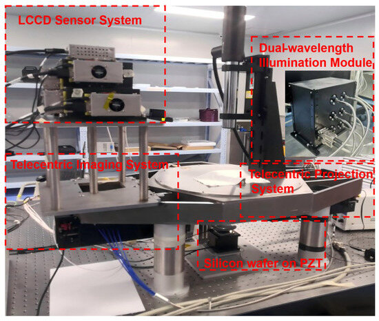
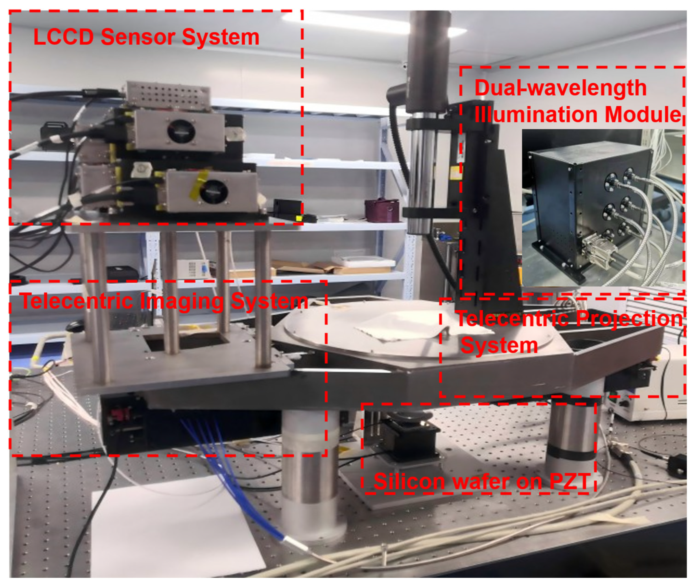
The experimental setup used for baseline validation is shown in Figure 13. The entire assembly is anchored to an air-floating vibration-isolation platform, effectively suppressing external disturbances. Under typical conditions, the platform maintains a vibration power spectral density below . The measurement path is illuminated by a dual-wavelength source composed of an 810 nm LED with a 32 nm bandwidth and a broadband 565 nm LED with a 104 nm bandwidth. In contrast, the reference path uses a single LED centered at 565 nm with the same 104 nm bandwidth.
Figure 13.
Experimental setup used for baseline validation of the proposed focus metrology system.
The wafer is mounted on a closed-loop piezoelectric translator (PZT) to provide controlled vertical motion during the experiment. The stage offers a resolution of 0.2 nm over a 50 μm stroke, with a repeatability of ±1 nm. These specifications help limit the influence of thermal drift and hysteresis, providing a stable mechanical basis for the repeated measurements and long-duration tests reported below.
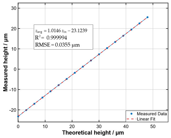
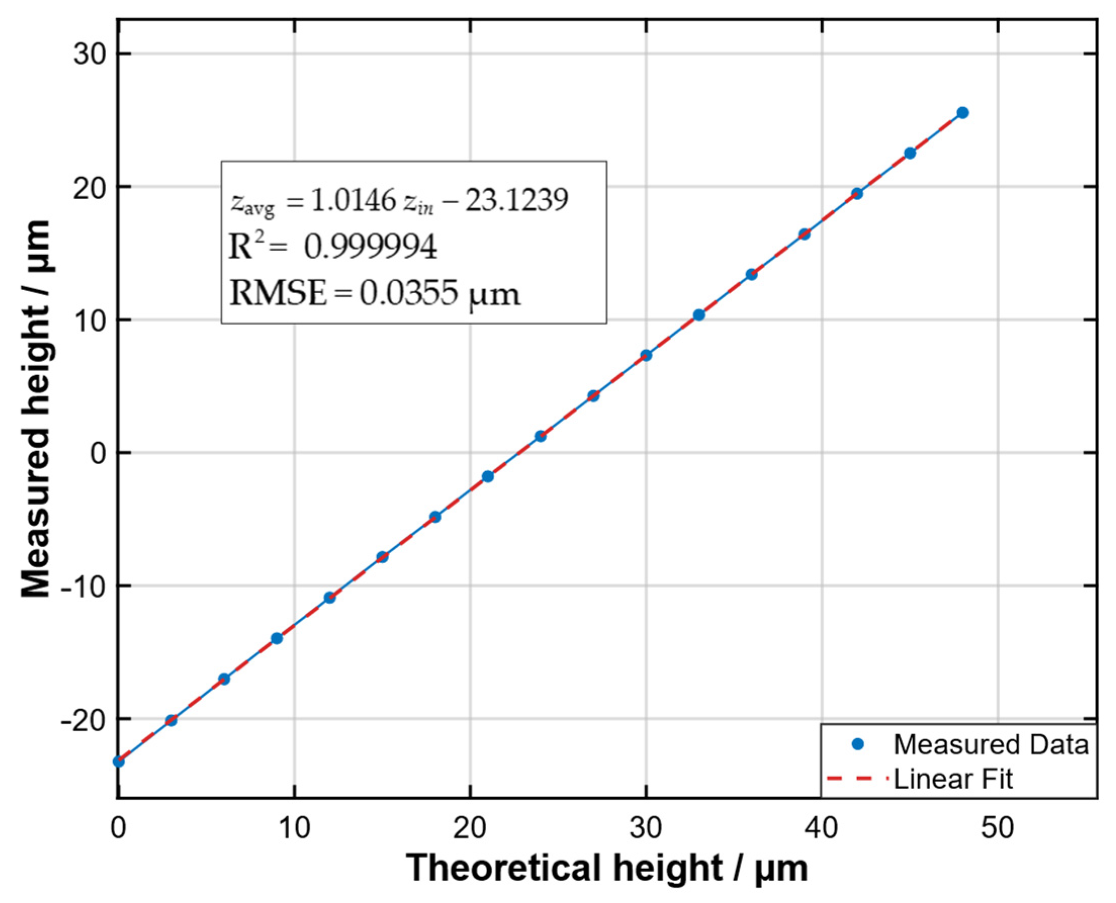
Before evaluating resolution, repeatability, and long-term stability, the height response of the system was first calibrated and its linearity was verified using the closed-loop PZT stage as the displacement reference. A series of known vertical displacements was applied to the wafer, and the corresponding height outputs were obtained from the complete signal-processing chain. The final measured value at each position was taken as the average of the five measurement channels. The resulting relationship between the theoretical input height, , and the averaged measured height output, , is shown in Figure 14. Here, denotes the average output of the five measurement channels at each input position.
Figure 14.
Linear relationship between the theoretical input height and the averaged measured height output of the proposed system.
Over the tested range, the measured response follows a clear linear trend. Linear fitting of the averaged output gives , with . The fitting residual has an RMSE of 0.0355 μm and a maximum absolute deviation of 0.0991 μm. These results indicate that the proposed system preserves a stable linear height response over the working range and provides a calibration basis for subsequent nanometer-level performance evaluation.
The fitted slope of 1.0146 indicates a small scale-factor deviation between the nominal displacement input and the measured height output. This should be distinguished from the linearity of the response itself. The high value, together with the small fitting residual, show that the system response follows a stable and highly repeatable linear trend over the tested range. The scale-factor deviation may arise from the displacement reference used in the calibration, or from the optical geometry of the measurement system, such as a small difference between the nominal and actual magnification, residual angular error, or detector installation tilt. Since this deviation is systematic, it can be compensated for by the linear calibration relation in Figure 14, or by position-wise calibration when a stricter linearity requirement is imposed. The following resolution, repeatability, and stability tests are therefore interpreted within the calibrated measurement domain.
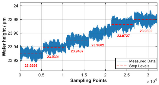
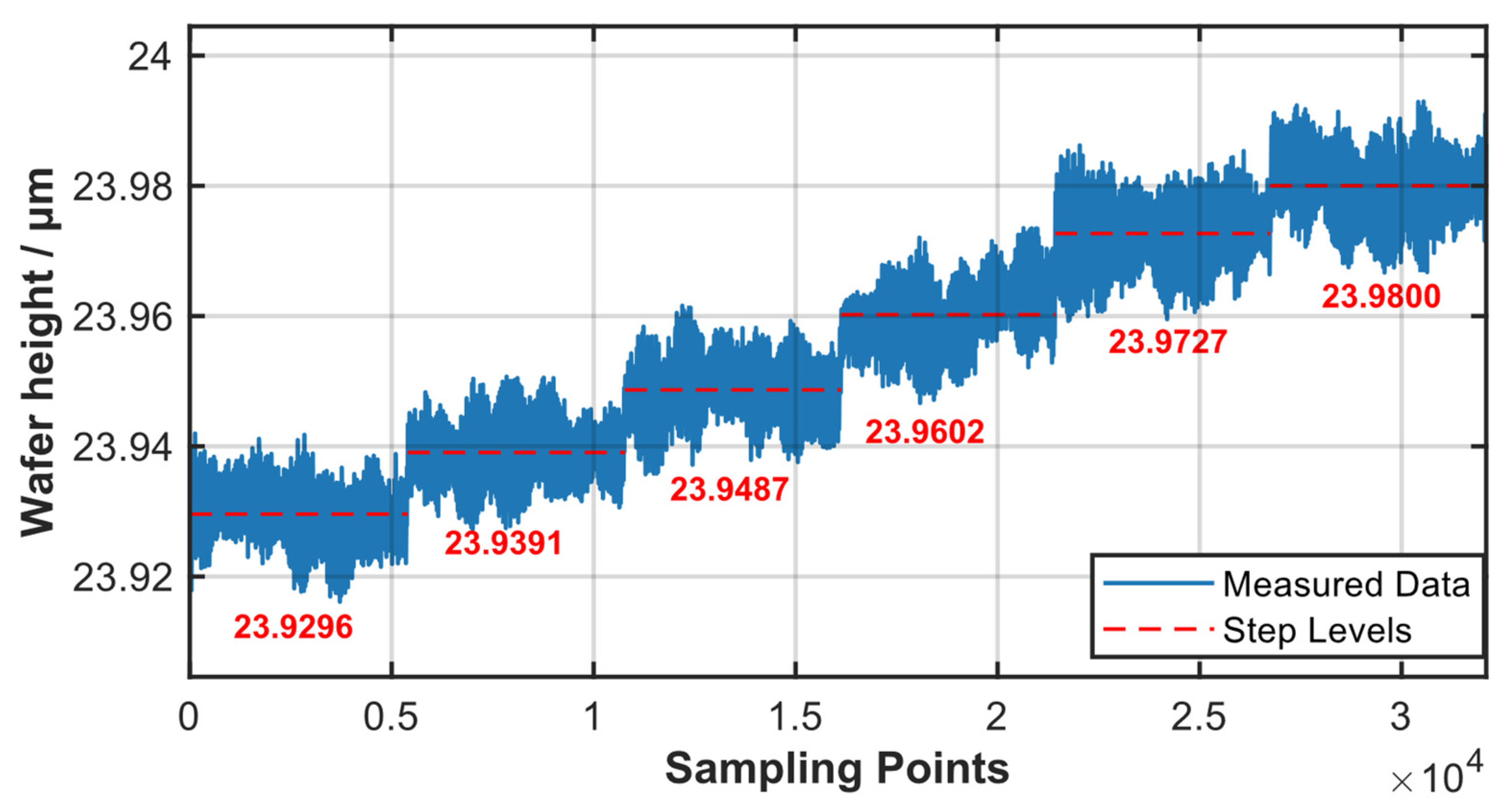
With the height response calibrated and its linearity verified, the next question is how small a vertical variation the system can resolve in practice. To examine this point, a high-precision closed-loop piezoelectric stage was used as the displacement reference to introduce controlled wafer-defocus steps to a bare silicon wafer. The stage has a nominal positioning resolution of 0.2 nm, which is much smaller than the programmed test steps used here; therefore, the applied 20 nm, 10 nm, and 5 nm inputs should be understood as prescribed test intervals rather than the motion limit of the stage. The corresponding height sequences were obtained from the complete LCCD-based signal-processing chain, as shown in Figure 15. The 20 nm and 10 nm inputs produced distinguishable step responses, with the output forming stable plateaus at each imposed height level, whereas the 5 nm input could not be consistently separated from the short-term fluctuation of the measurement sequence. Based on this comparison, the effective vertical resolution of the proposed system was determined to be 10 nm under the bare-silicon baseline condition.
Figure 15.
Measured system response for vertical resolution characterization.
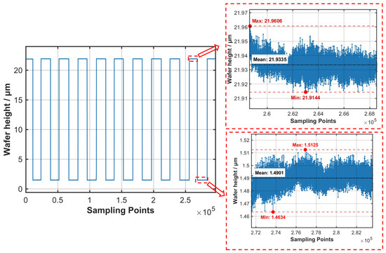
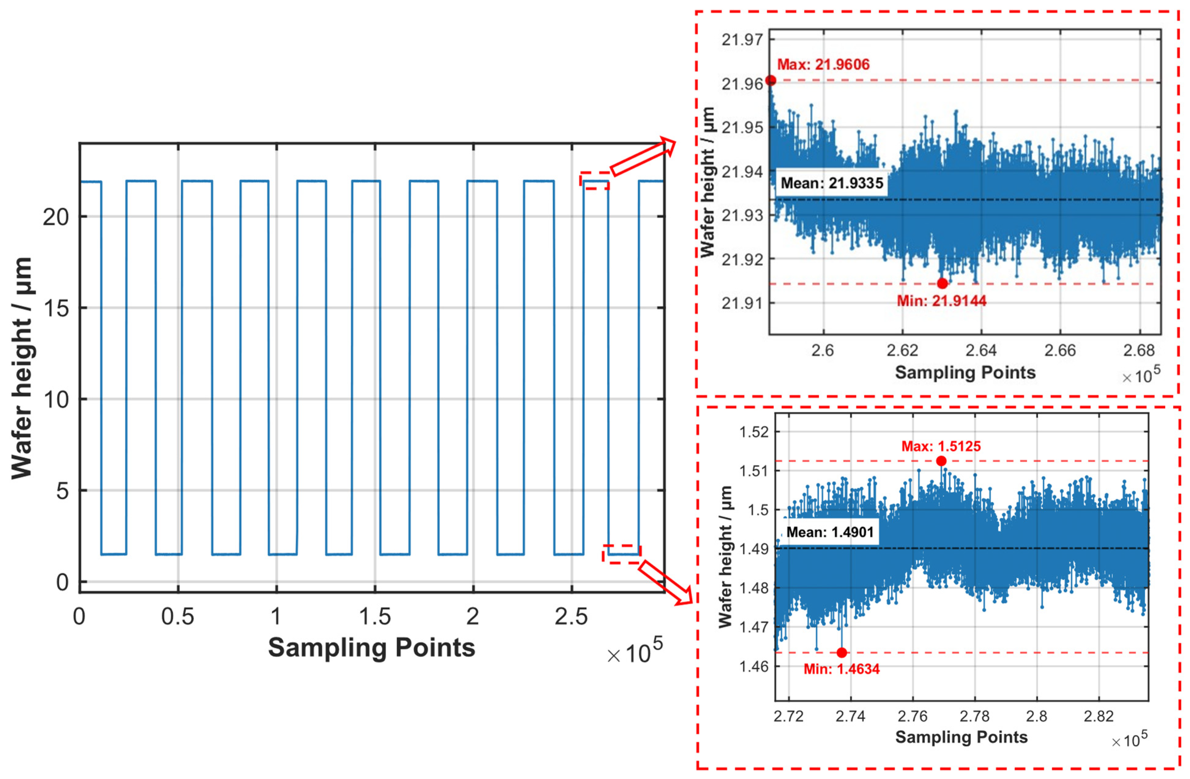
System repeatability was assessed by repeatedly moving the wafer between two prescribed vertical setpoints with the piezoelectric stage. After each return, the output signal was recorded once the stage had settled, so that the responses at the high and low positions could be tracked over multiple cycles. Figure 16 shows the corresponding measurement traces. Throughout the repeated switching process, the two position levels remained clearly distinguishable, and no obvious degradation in return consistency was observed. To make this behavior quantitative, the mean value of the stable segment was extracted for each return cycle, and the resulting high- and low-position mean values are listed in Table 4.
Figure 16.
Repeatability evaluation based on repeated wafer height measurements.
Table 4.
Measured repeatability performance of the proposed system.
Based on the mean values given in Table 4, the repeatability of the system was further characterized using both peak-to-valley and RMS-based metrics, as summarized in Table 5. In engineering peak-to-valley form, the repeatability is 32 nm at the high position and 35 nm at the low position. The corresponding standard deviations are 11.18 nm and 10.04 nm, while the RMS deviations are 10.61 nm and 9.53 nm. These results indicate that the system maintains good return-to-position consistency under bare-silicon conditions. In the discussion that follows, the peak-to-valley values are retained as practical repeatability indicators, whereas the RMS-based metrics are used as the more suitable statistical quantities for comparison with the modeled internal uncertainty.
Table 5.
Statistical repeatability metrics derived from the stable-segment mean values of repeated return measurements.
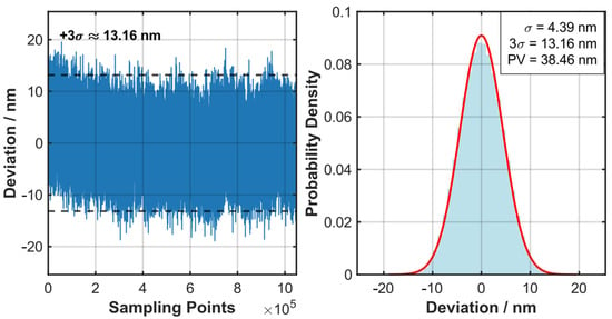
System stability was assessed by holding the wafer at a fixed vertical position while continuously acquiring measurement data over an extended period. This acquisition captures the temporal noise and drift characteristics of the complete measurement chain. Stability was quantified as three times the standard deviation of the accumulated height measurements. The statistical results, summarized in Figure 17, indicate a 3σ stability of 13.16 nm, reflecting robust measurement consistency during prolonged operation.
Figure 17.
Stability evaluation of the experimental system over sampling points. The blue curve shows the measured height-deviation sequence, the light-blue shaded area represents the probability-density histogram of the measured deviations, and the red curve denotes the Gaussian fitting result.
The experimental results under bare-silicon conditions make the baseline behavior of the proposed system relatively clear. The measured resolution, repeatability, and long-term stability show that the optical configuration and the LCCD-based localization strategy can support nanometer-level focus measurement without relying on a smaller detector pitch. The repeated return measurements are particularly useful in this respect because they reflect how consistently the system returns to the same height state over multiple cycles. In peak-to-valley form, the repeatability is 32 nm at the high position and 35 nm at the low position. When the stable-segment mean values are examined in statistical form, the corresponding RMS deviations are 10.61 nm and 9.53 nm. These RMS-based results are more suitable than the peak-to-valley values for comparison with the modeled internal uncertainty.
It is also important to keep the scope of these experiments in view. They were carried out on a bare silicon wafer, not to reproduce the full process condition of resist-coated wafers, but to separate the intrinsic performance of the instrument from the additional disturbance introduced by thin-film interference. For that reason, the present measurements should be understood mainly as a baseline validation of the system itself. In the same sense, the RMS values obtained from the repeated return measurements are lower than the modeled internal uncertainty of 23.43 nm because the latter represents a broader uncertainty budget that combines detector-side and algorithm-related contributions under the adopted operating condition, whereas the experimental results reflect return-to-position behavior under a specific bare-silicon baseline test. The thin-film-related contribution discussed in Section 4, therefore, remains a model-based estimate for coated-wafer conditions, while the bare-silicon results reported here correspond more directly to the intrinsic measurement stability of the instrument. Seen in this way, the present experiments do not close the full problem in a single step, but they do establish a reliable baseline from which coated-wafer validation can proceed more directly.
6. Conclusions
This study presents a dual-wavelength optical triangulation system for focus metrology in 350 nm lithography, together with a two-stage sub-pixel localization strategy and a unified uncertainty analysis framework. A central aim of the work was to separate the intrinsic performance of the instrument from the additional uncertainty introduced by thin-film effects under practical wafer conditions. With that distinction in mind, the different parts of the study play different roles. The thin-film model is used to examine how dual-wavelength illumination reduces the equivalent height fluctuation associated with photoresist interference, while the covariance-based analysis clarifies the contributions of quantization, interpolation, noise, and response non-uniformity within the LCCD-based localization chain. The experiments, by contrast, were carried out on a bare silicon wafer in order to establish the system baseline under conditions where photoresist-induced interference is absent. Under these conditions, the prototype achieved a vertical resolution of 10 nm, a repeatability of 35 nm, and a stability of 13.16 nm.
What the present results make clear is the baseline capability of the proposed system. Under bare-silicon conditions, the instrument already shows stable nanometer-level measurement performance without relying on a reduced detector pitch. Once resist-coated wafers are considered, the remaining thin-film-related residual becomes an additional factor that can no longer be ignored, and its influence has been estimated here through model-based analysis. The point of the present work is therefore not that the full problem has already been closed experimentally, but that the foundation is now in place: the system baseline has been established, the main uncertainty contributions have been sorted out, and the role of dual-wavelength suppression under coated-wafer conditions can be evaluated within the current framework. The next stage will focus on direct validation with wafers carrying representative photoresist stacks, so that the practical performance of the system can be assessed under conditions closer to actual lithographic processing.
Author Contributions
Conceptualization, H.G. and X.L.; methodology, H.G.; software, X.L.; validation, H.G., X.Z. and D.K.; formal analysis, H.G.; investigation, H.G.; resources, M.S., M.L. and J.H.; data curation, Y.C. and X.Z.; writing—original draft preparation, H.G.; writing—review and editing, M.S.; visualization, H.G.; supervision, M.S.; project administration, M.S. and M.L.; All authors have read and agreed to the published version of the manuscript.
Funding
This research received no external funding.
Data Availability Statement
The data underlying the results presented in this paper are not publicly available at this time but may be obtained from the authors upon reasonable request.
Conflicts of Interest
The authors declare no conflicts of interest.
References
- Qi, Y.; Pei, Y.; Zong, M.; Li, J.; Chen, J. Research Progress of Lithography Focusing and Leveling Measurement Technology. Laser Optoelectron. Prog. 2022, 59, 0922015. [Google Scholar] [CrossRef] [Scilit]
- Buck, P.D.; Rieger, M.L. Phase-shift mask applications. In Optical/Laser Microlithography IV; SPIE: San Jose, CA, USA, 1991; Volume 1463, pp. 218–228. [Google Scholar] [CrossRef] [Scilit]
- Feng, J.; Tang, Y.; Xie, Z.; Du, J.; Gong, J. Coaxial focusing method based on differential modulation evaluation. Acta Opt. Sin. 2021, 41, 0612001. [Google Scholar] [CrossRef] [Scilit]
- Wang, X.; Dai, F. Integrated Circuit and Lithographic Tool; Science Press: Beijing, China, 2020. [Google Scholar]
- Jang, J.H.; Park, T.; Park, K.D.; Hwang, J.H.; Choi, J.P.; Kang, Y.S. Focus control budget analysis for critical layers of flash devices. In Metrology, Inspection, and Process Control for Microlithography XXVIII; SPIE: San Jose, CA, USA, 2014; Volume 9050, pp. 647–653. [Google Scholar] [CrossRef] [Scilit]
- Sun, Y. Research on Focusing and Leveling System in Nanolithography. Ph.D. Thesis, University of Chinese Academy of Sciences, Beijing, China, 2016. [Google Scholar]
- Sun, Y.; Li, S.; Ye, T.; Zong, M. Process dependency of focusing and leveling measurement system in nanoscale lithography. Acta Opt. Sin. 2016, 36, 0812001. [Google Scholar] [CrossRef] [Scilit]
- Kawashima, H.; Suzuki, A. Method and Apparatus for Precisely Detecting Surface Position of a Patterned Wafer. U.S. Patent 5,118,957, 2 June 1992. [Google Scholar]
- Yu, D.; Liu, J.; Zhou, J.; Sun, H.; Jin, C.; Wang, J. Depth–Depth of Focus Moiré Fringe Alignment via Broad-Spectrum Modulation. Photonics 2024, 11, 138. [Google Scholar] [CrossRef] [Scilit]
- den Boef, A.J. Optical wafer metrology sensors for process-robust CD and overlay control in semiconductor device manufacturing. Surf. Topogr. Metrol. Prop. 2016, 4, 023001. [Google Scholar] [CrossRef] [Scilit]
- Wang, P.; Meng, F.; Zhang, Z.; Wang, D.; Wang, S.; Yao, E.; Wang, L.; Ye, R. A bump height measurement method based on optical triangulation. Acta Photonica Sin. 2022, 51, 0512001. [Google Scholar] [CrossRef] [Scilit]
- Yan, W.; Yang, Y.; Chen, W.; Hu, S.; Zhou, S. Moiré-based focusing and leveling scheme for optical projection lithography. Appl. Opt. 2010, 49, 5959–5963. [Google Scholar] [CrossRef] [Scilit]
- Zhu, X.; Hu, S.; Zhao, L. Wafer focusing measurement of optical lithography system based on Hartmann–Shack wavefront testing. Opt. Lasers Eng. 2015, 66, 128–131. [Google Scholar] [CrossRef] [Scilit]
- Liu, J.; Li, Q.; Liu, J.; Hu, S.; Qi, C. Fast wafer focus measurement system for photolithography using on-axis structure illumination method. Opt. Lasers Eng. 2023, 162, 107412. [Google Scholar] [CrossRef] [Scilit]
- Nan, Z.; Tao, W.; Zhao, H. Automatic optical structure optimization method of the laser triangulation ranging system under the Scheimpflug rule. Opt. Express 2022, 30, 18667–18683. [Google Scholar] [CrossRef] [Scilit]
- Cui, H.; Li, X.; Cong, R.; Bai, J.; Du, J. Real-time uncertainty reduction in laser triangulation via dynamic speckle correlation. Measurement 2024, 234, 114842. [Google Scholar] [CrossRef] [Scilit]
- Zhao, H.; Liu, X.; Wang, S.; Diao, K.; Luo, C. An enhanced centerline extraction algorithm for complex stripes in linear laser scanning measurement. Precis. Eng. 2024, 91, 199–211. [Google Scholar] [CrossRef] [Scilit]
- Tang, Y.; He, Y.; Yang, Y.; Wang, J.; Liu, J.; Yan, W. Nano-focusing and leveling system based on improved phase analysis. IEEE Photonics J. 2016, 8, 1–7. [Google Scholar] [CrossRef] [Scilit]
- Jiang, W.; Wang, H.; Xie, W.; Qu, Z. Lithography Alignment Techniques Based on Moiré Fringe. Photonics 2023, 10, 351. [Google Scholar] [CrossRef] [Scilit]
- Guan, H.; Lei, X.; Chu, Y.; Zhao, X.; Kuang, D.; Ling, M.; Song, M.; Hong, J. High-Speed and High-Precision Algorithm for LCCD-Based Triangulation Height Measurement. J. Phys. Conf. Ser. 2025, 3083, 012008. [Google Scholar] [CrossRef] [Scilit]
- Zhang, Z.; Li, Y.; Gao, F.; Gao, N.; Meng, Z.; Jiang, X. Phase unwrapping technology for structured light three-dimensional measurement: A review (invited). Infrared Laser Eng. 2023, 52, 20230126. [Google Scholar] [CrossRef] [Scilit]
- Shen, Y.; Kong, L.; Tang, X.; Song, H.; Hua, S.; Ding, Z. Large Depth-of-Field Structured Light System for 3D Microscale Measurement with Integrated Speckle Denoising. Opt. Laser Technol. 2025, 192, 113688. [Google Scholar] [CrossRef] [Scilit]
- Jin, C.; Yu, D.; Sun, H.; Liu, J.; Zhou, J.; Wang, J. An Adjustment Strategy for Tilted Moiré Fringes via Deep Q-Network. Photonics 2024, 11, 666. [Google Scholar] [CrossRef] [Scilit]
- Li, X.; He, J.; Xu, G.; Wu, X.; Wu, J. Nanoscale Displacement Measurement Method and Device Design Based on Moiré Fringe Amplification. Measurement 2026, 257, 118811. [Google Scholar] [CrossRef] [Scilit]
- Cao, Y.; Ma, D.; Li, H.; Cui, G.; Zhang, J.; Yang, Z. Review of Industrialization Development of Nanoimprint Lithography Technology. Chips 2025, 4, 10. [Google Scholar] [CrossRef] [Scilit]
- Im, J.; Lee, H.; Jang, K.; Choi, S. White-light colorimetric interferometry for measurement of thickness and topography on semiconductor structures. Sci. Rep. 2025, 15, 41902. [Google Scholar] [CrossRef] [Scilit] [PubMed]
- Münch, F.; Hauer, B.; Breunig, I.; Carl, D. Multi-angle averaging approach for measuring the coating thickness on thin transparent polymer films. Appl. Spectrosc. 2025, 79, 1615–1624. [Google Scholar] [CrossRef] [Scilit] [PubMed]
- Wang, J.; Peng, L.; Zhai, F.; Tang, D.; Gao, F.; Zhang, X.; Chen, R.; Zhou, L.; Jiang, X.J.J. Polarized angle-resolved spectral reflectometry for real-time ultra-thin film measurement. Opt. Express 2023, 31, 6552–6565. [Google Scholar] [CrossRef] [Scilit] [PubMed]

Disclaimer/Publisher’s Note: The statements, opinions and data contained in all publications are solely those of the individual author(s) and contributor(s) and not of MDPI and/or the editor(s). MDPI and/or the editor(s) disclaim responsibility for any injury to people or property resulting from any ideas, methods, instructions or products referred to in the content. |
© 2026 by the authors. Licensee MDPI, Basel, Switzerland. This article is an open access article distributed under the terms and conditions of the Creative Commons Attribution (CC BY) license.