


Abstract
To address the demand for low-cost, low-loss, and environmentally friendly optical power dividers in short-range visible light communication (VLC) systems, a low-loss 1 × 2 Y-branch optical splitter based on the integration of a planar optical waveguide (POW) and plastic optical fiber (POF) is proposed and experimentally demonstrated. The device employs a large-core step-index POF with a core diameter of 1 mm, enabling efficient coupling of multimode optical signals. The design and structural optimization of the 1 × 2 POF splitter are simulated by the beam propagation method (BPM). We fabricated the device through a low-cost manual assembly process, followed by packaging and experimental characterization. Measurements at 650 nm on ten samples show a minimum insertion loss of 3.4 dB and a lowest excess loss of 0.8 dB. The splitting ratio ranges from 49.6%:50.4% to 37%:63%, with a minimum uniformity of 0.06, indicating stable power distribution performance. These results confirm that a simple, low-cost fabrication approach can achieve practical optical performance, offering a feasible route toward scalable polymer-based photonic integration.
1. Introduction
As visible light communication (VLC) continues to evolve in applications such as high-speed indoor access, smart home systems, and vehicular networks, there is a growing demand for optical interconnection solutions that are cost-effective, reliable, and easy to deploy [1,2]. Compared with traditional radio frequency (RF) communication, VLC offers several advantages, including abundant spectrum resources, strong immunity to electromagnetic interference, and enhanced security [3,4]. However, the overall performance of VLC systems is largely determined by the efficiency and stability of the optical transmission links, especially the performance of passive distribution components [2,5,6]. Therefore, the development of low-loss, low-cost optical power splitter networks (ODNs) for short-range applications remains a key challenge in the practical deployment of VLC.
For various passive devices, the 1 × 2 optical splitter is the most basic functional unit. It is widely used for signal distribution, system monitoring, redundancy protection, and network configuration. Plastic optical fiber (POF) has a large core diameter (0.5–1 mm), a high numerical aperture (NA ≈ 0.5), good mechanical flexibility, and a low fabrication cost. Because of these features, POF serves as a favorable transmission medium for short-distance visible light communication (VLC) [7,8]. In the visible wavelength range (380–780 nm), especially near 650 nm, polymethyl methacrylate (PMMA)-based POF shows relatively low attenuation (about 0.15–0.25 dB/m) and good mechanical strength [9]. These properties make POF well suited for home networking, vehicular communication, and industrial interconnections [1,9]. Therefore, efficient and cost-effective POF-based optical power splitters are needed to enable large-scale VLC systems.
From a fabrication standpoint, conventional 1 × 2 POF splitters are mostly made using fused biconical taper (FBT) or photolithography-based planar waveguide technologies. FBT is a well-established method, but its use for POF is limited by the poor thermal stability of polymer materials and the multimode nature of large-core fibers. These issues can lead to structural inconsistency and higher insertion loss [10]. Photolithographic waveguides, on the other hand, provide high fabrication precision. However, they suffer from a large mode-field mismatch with millimeter-scale POF cores. In addition, their need for cleanroom-based processes raises fabrication complexity and cost [11,12]. POW technology offers a different route. It allows for flexible optical path design and a higher degree of integration on a substrate [11,13]. In this way, making a 1 × 2 POF splitter with a POW structure can maintain good optical performance and reduce manufacturing costs, which helps move VLC optical components forward.
From a physical perspective, large-core step-index POFs work as highly multimode waveguides. They support hundreds to thousands of guided modes. Differences in propagation constants among these modes lead to strong intermodal dispersion. This dispersion causes pulse broadening and sets a limit on the achievable system bandwidth [14,15]. The relationship between bandwidth and length of a step-index multimode fiber can be approximated as:
where is the core refractive index, and L is the transmission length. For a typical PMMA POF with a core diameter of 1 mm, the bandwidth–length product is on the order of 10–100 MHz·100 m. This limitation means that when designing POF-based devices, one must consider not only optical power distribution but also how structural parameters affect modal evolution and bandwidth performance. In this setting, 1 × 2 Y-branch POF splitters are well suited for large-core multimode fiber systems. Their simple geometry and controllable power division make them attractive [11,16,17]. Still, their performance is strongly affected by the geometric features of the branching region. These features include the branch angle, transition length, and waveguide profile. Such parameters control mode coupling and conversion processes. As a result, they influence insertion loss, splitting uniformity, and modal dispersion. Thus, the Y-branch geometry is critical for both power distribution and the system’s effective transmission bandwidth.
Based on the above considerations, a low-loss 1 × 2 Y-branch POF splitter with a POW structure is proposed, simulated, and experimentally tested. The device uses a PMMA fiber with a 1 mm core diameter. Key structural parameters such as the branch angle, transition length, and refractive index distribution are optimized with BeamPROP. This optimization aims to balance low insertion loss with uniform power splitting. The POW splitter is made using a simple manual process combined with ultraviolet (UV) curing. This method lowers fabrication cost and maintains stable optical performance.
In this paper, we first present a low-loss 1 × 2 Y-branch POF splitter based on a planar optical waveguide (POW). Second, we introduce the material properties of POF and the key performance parameters used for device characterization. Third, we establish a device model, optimize the structural parameters of the 1 × 2 POF splitter, and carry out simulation analysis using RSoft (version 2018.12). Fourth, we describe the fabrication process, experimental methods, and measurement results. Fifth, we discuss the obtained results, including discrepancies between simulation and experiment, influencing factors, performance limitations, and potential improvements. Finally, we summarize the main findings, evaluate the device performance, and outline directions for future research.
2. Materials and Methods
2.1. PMMA POF
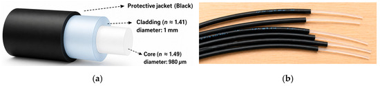
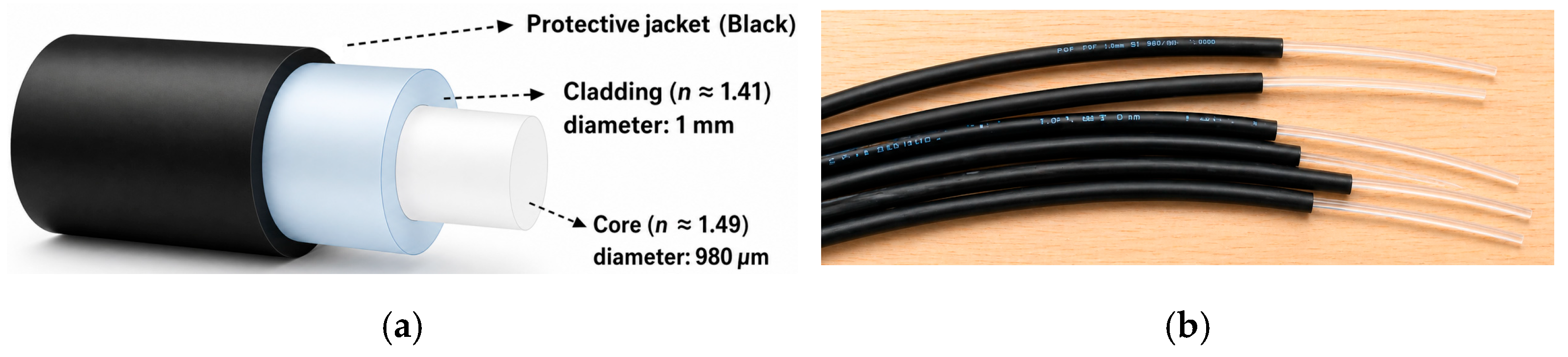
We used a large-core step-index POF with a core diameter of 1 mm to fabricate the 1 × 2 splitter in this study. The POF has a numerical aperture (NA) of about 0.5 and its core refractive index is around 1.49, and the cladding is made of a fluorinated polymer with a refractive index of about 1.41. This gives a refractive index difference (Δn) of roughly 0.08 [18,19]. This relatively large index contrast helps the total internal reflection (TIR) work well at the core–cladding interface. As a result, the optical field stays confined inside the core region, and radiation loss and inter-channel crosstalk are reduced. PMMA has good optical transparency in the visible range (about 380–780 nm). Its typical attenuation coefficient at 650 nm is about 0.2 dB/m [1,20]. The structure of the PMMA fiber is shown in Figure 1a, and physical samples of the fiber are shown in Figure 1b. In addition, PMMA works well with various UV-curable polymers and shows good adhesion to them. This property is useful for later waveguide fabrication and device integration [21].
Figure 1.
The PMMA fiber (a) structure and (b) physical samples.
2.2. Performance Metrics of POF Splitters
POF splitters are key passive components in short-range optical communication systems, and their performance has a direct impact on the stability, power budget, and transmission efficiency of optical signals [10,15,22]. The main evaluation metrics include insertion loss, excess loss, splitting ratio, and splitting uniformity for a 1 × 2 POF splitter. These metrics provide the basic criteria for device design, fabrication, and performance characterization.
Insertion loss (IL) measures the drop in optical power when an input signal travels through the splitter and reaches a given output port. This loss reflects the total power lost during transmission, coupling, and power division. The insertion loss for the i-th output port is defined as:
where denotes the input optical power, and represents the optical power at the i-th output port. A lower IL value means less transmission loss and higher device efficiency.
Excess loss (EL) describes the extra loss on top of the theoretical splitting loss and reflects the internal quality of the splitter structure. It is defined as follows:
EL comes mainly from radiation leakage, scattering at the Y-branch junction, and flaws in the tapered transition region. These flaws include material inhomogeneity or fabrication defects. EL is strongly affected by structural symmetry, taper design choices, and fabrication precision. For this reason, EL is a key measure of device quality and reproducibility in large-scale manufacturing.
The splitting ratio (SR) describes how optical power is distributed among the output ports of the splitter. It is given by the expression below:
Changes in SR stem largely from asymmetry in the waveguide structure, errors in manufacturing, and wavelength dependence. The SR directly shows how well the device can distribute optical power. Hence, the SR is a key indicator for judging whether the device provides uniform power distribution.
The uniformity (SU) measures the difference in optical power distribution between the two output ports. SU shows the device’s ability to keep power distribution uniform under different working conditions. These conditions include temperature changes and optical power fluctuations. SU is therefore an important measure of long-term operational stability for POF splitters. SU is defined as follows:
A smaller SU value points to a narrower range of fluctuation. This means the device has better splitting uniformity and more stable power distribution.
3. Device Design and Simulation
3.1. Device Design
Our design employs the BeamPROP module of RSoft software for POW structure simulation and performance optimization. The design goal of the 1 × 2 Y-branch POF splitter is to minimize radiation loss and achieve uniform power distribution while ensuring smooth multimode beam splitting. In this paper, the beam propagation method (BPM) based on the scalar approximation is used for simulation, allowing for direct observation of the evolution of the optical field along the propagation direction.
The BPM transforms the scalar Helmholtz equation into a paraxial propagation form by progressively advancing the light field distribution, as shown in the following equation.
where is the optical field envelope, is the transverse Laplace operator, is the refractive index perturbation, and is the vacuum wavenumber.
The core assumptions of the BPM are highly compatible with the adiabatic design principle, enabling accurate simulation of the adiabatic transmission and symmetrical splitting process of the input fundamental mode in the tapered region [23]. This implies that the relative change in the optical field envelope within a single mode beat length is sufficiently weak, thereby suppressing coupling of fundamental mode energy to higher-order modes and reducing radiation loss [24,25]. The corresponding condition is expressed as:
where is the equivalent width of the waveguide, and is the mode beat length.
The POW structure of the Y-type 1 × 2 POF splitter mainly consists of three parts, which include the input waveguide, the tapered transition region, and the two output waveguides. The core of the structural design is to reduce optical loss, ensure splitting uniformity, and accommodate manual fabrication processes, thereby lowering the difficulty of manual operation while balancing low cost and low loss. The dimensions of the input and two output waveguides need to match the 1 mm large-core PMMA fiber. Therefore, the waveguide diameter is set to 1 mm to ensure efficient optical signal coupling and reduce manual alignment difficulty. The waveguide substrate is made of PMMA (the refractive index is 1.41), and the tapered region is filled with Epo-Tek OG603 UV-curable adhesive (Epoxy Technology, Inc., Billerica, MA, USA). The OG603 UV achieves 98% transmittance in the 420–1600 nm wavelength range, with an uncured refractive index of 1.4734 and a cured refractive index of 1.5037 in the visible light range, and the refractive index is close to that of the waveguide core material, enabling a smooth refractive index transition at the bonding interface, reducing Fresnel reflection and light leakage caused by abrupt index changes, and thus effectively minimizing additional interface losses [19,22,26].
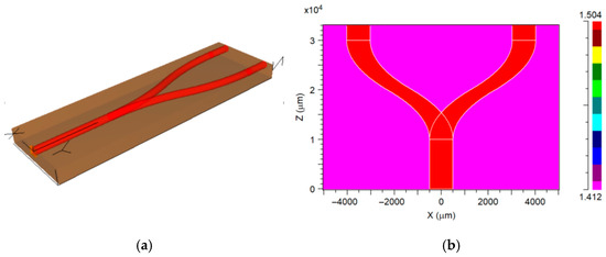
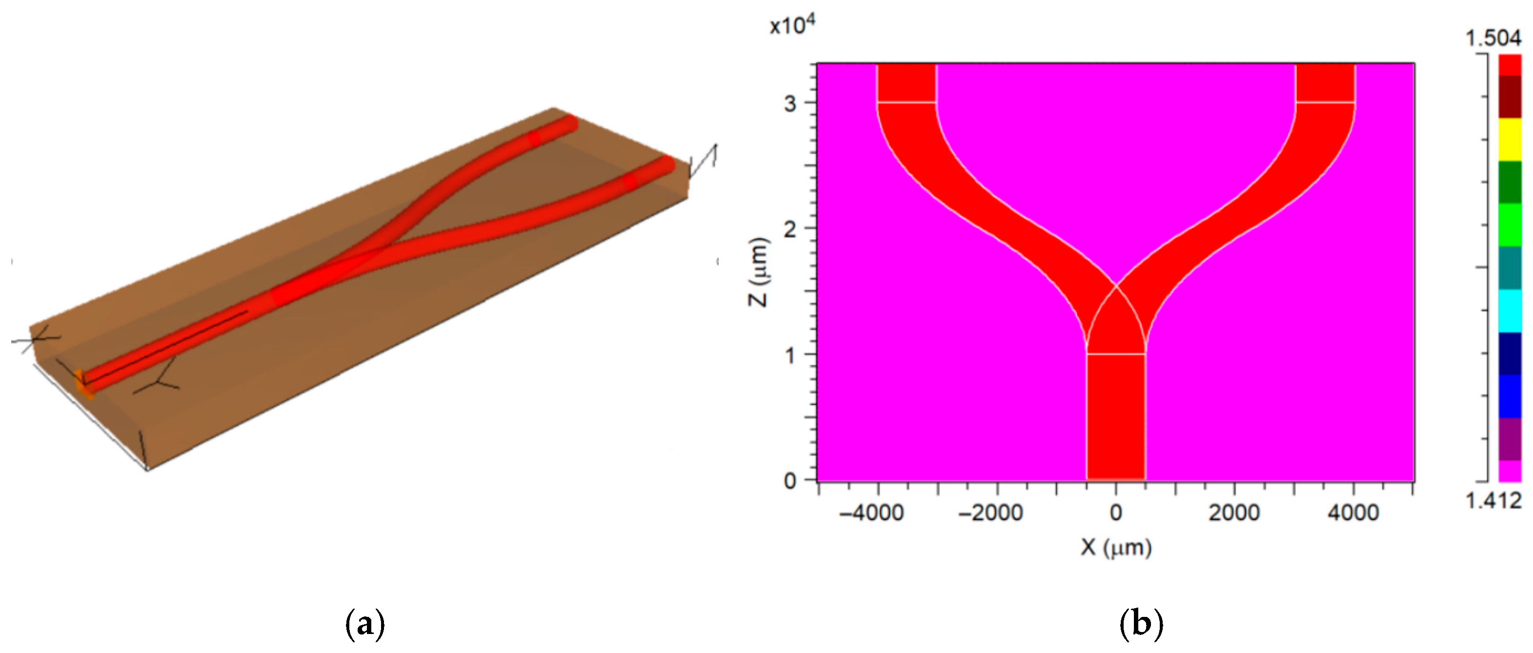
The 1 × 2 POF splitter based on POW adopts a symmetrical design, and its 3D structure is shown in Figure 2a. The initial design angle of the Y-branch was 15°. However, to ensure consistency between simulation and performance optimization, the entire Y-branched region was filled with OG603 adhesive for simulation. The refractive index distribution of the 1 × 2 POF splitter obtained from BPM simulation is presented in Figure 2b.
Figure 2.
The (a) simulation structure and (b) refractive index distribution of the 1 × 2 POW splitter.
In the 1 × 2 POF splitter based on POW, the input waveguide gradually splits into two output arms. When light waves enter the branching region from the input waveguide, the energy is evenly distributed to the two output waveguides through an adiabatic gradient structure [25,27]. To reduce radiation loss and mode mismatch loss in the branching region, the branching angle, tapered region length, and device dimensions must be rationally designed [17,22,28]. Therefore, this paper achieves low-loss and uniform beam splitting mainly by optimizing the splitting angle and the length of the tapered region.
3.2. Device Simulation and Optimazation
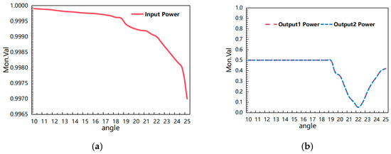
The splitting angle of Y-type 1 × 2 POF splitters has the most significant impact on radiation loss. A splitting angle that is too small results in an excessively long device, hindering integration, whereas an angle that is too large leads to abrupt mode field changes and increased radiation loss [26,29]. Therefore, to determine the optimal splitting angle for the Y-branch structure, a full-range simulation was performed over an angle range of [10°, 25°] to analyze the changes in optical power at the input and output ports of the Y-type power splitter at a wavelength of 650 nm. The simulation results show that the optical signal propagates smoothly within the planar waveguide, with minimal input power loss: approximately 99.7% of the input power is maintained, and no significant optical leakage is observed (see Figure 3a). The optical power distribution at the Y-branch is uniform, with the power ratio of the two output ports approaching 1:1. When the splitting angle θ is less than 19°, there is virtually no loss in the output optical power at the two ports. When θ exceeds 19°, the output power first decreases significantly and then increases again, indicating that a larger bifurcation angle leads to increased light scattering loss, which is seen in Figure 3b.
Figure 3.
Variation of (a) input power and (b) output power with the splitting angle.
Because a small splitting angle would result in an excessively large device size, which significantly increases the difficulty of injection molding and manual finishing, a splitting angle of θ = 17° was ultimately selected as the optimal value, balancing minimal loss with process feasibility.
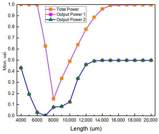
After setting the optimal splitting angle to 17°, we performed simulations for the bifurcation length over the range of 4 mm to 20 mm. These simulations were performed to see how the optical power changes at the input and output ports of the POF splitters. The simulation results show that the optical signal moves through the bifurcation region most smoothly when the bifurcation length is between 16 mm and 20 mm. There is almost no extra loss in this range, so the transmission efficiency is at its best, as shown in Figure 4. Finally, we chose a bifurcation length of 17 mm. This choice takes into account the need to make the device small and the practical limits of manual injection molding, which reduces the overall device size while still maintaining low-loss performance.
Figure 4.
The variation in input and output power with the bifurcation length.
3.3. Device Simulation Analysis
The tapered transition region of the 1 × 2 POF splitter is the bifurcation structure, which connects the input waveguide and the output waveguide. This region allows optical modes to change smoothly. It helps avoid sudden mode changes at the bifurcation point, and in doing so, it reduces scattering loss. With the parameters we optimized, the specific structural parameters used in the simulation are as follows: the input waveguide length is 10 mm, the splitting angle is 17°, the bifurcation region length is 17 mm, and the output waveguide length is 3 mm. The design not only keeps optical signal transmission stable, but also leaves enough room for manual filling with the UV-cured epoxy resin adhesive OG603.
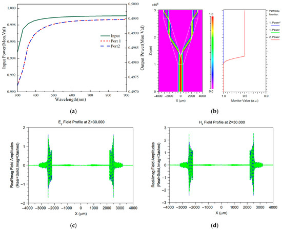
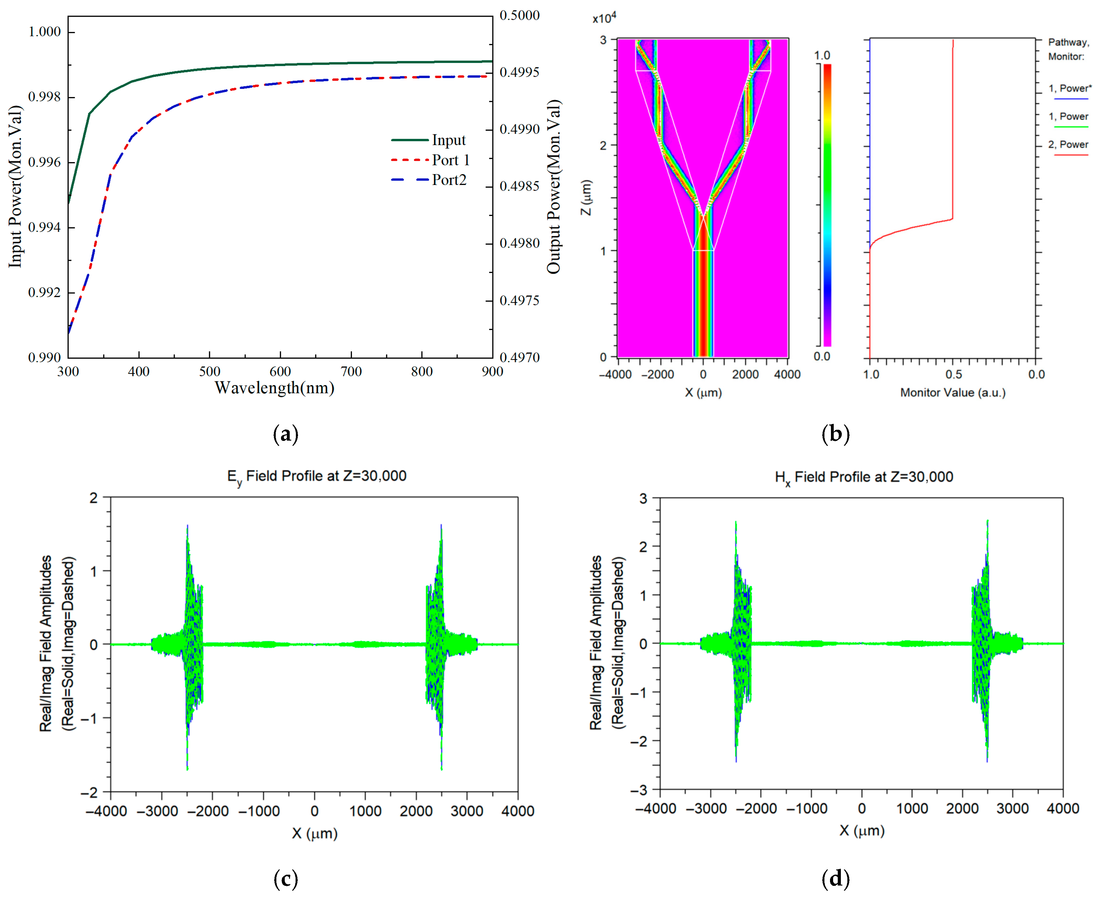
We scanned the wavelength from 300 to 900 nm to test the device’s use in the visible range (Figure 5a). Inside the operating window of the POF splitter from 380 to 780 nm, the output splitting ratio stays close to 50%:50%. This result points to good structural symmetry and little dependence on wavelength. At the same time, the normalized power loss at the input stays below 0.1% and that at the output ports stays below 0.05%, which shows that the loss is low. In the range from 300 to 380 nm, the loss increases by less than 0.6% for the input and less than 0.3% for the output. This small loss comes from stronger material absorption and changes in the mode field. These results confirm that the proposed 1 × 2 POF splitter has good broadband performance in the visible range, and its splitting is especially stable and its loss is low inside the 380–780 nm band.
Figure 5.
The (a) normalized input and output power variation over the wavelength range of 300–900 nm, (b) field distribution of the normalized optical power of the 1 × 2 POF splitter during propagation, and (c) electric field distribution and (d) magnetic field distribution at the two output ports Z = 30,000 μm.
We used the slab mode approximation model in BPM to simulate and analyze the 1 × 2 Y-branch POF splitter at an incident wavelength of 650 nm, and the results are shown in Figure 5b. The aim was to see how structural parameters affect optical field splitting and power distribution. The input optical power is concentrated in the central waveguide (near X ≈ 0). When the light reaches the splitting region (near Z ≈ 15,000 mm), the optical field spreads out symmetrically into the two arms of the Y-junction. After that, the output power is confined in the two output waveguides (near X ≈ ±2.5 mm) and stays stable. The field strength outside the waveguides is very small, which indicates that the optical field is well confined, radiation loss is low, and no mode distortion occurs. The normalized optical power changes along the propagation path as follows. The normalized optical power along the propagation direction is shown in Figure 5b, where “1,power*” represents the total input power, “1,power” represents the output power at port 1, and “2,power” represents the output power at port 2. When the input power is set to 1 a.u., the power in both output channels stays at 0.5 a.u. without any fluctuation. This confirms that the beam splitting behavior converges and that long-term stability is good. We obtained and analyzed the Ey electric field distribution (Figure 5c) and the Hx magnetic field distribution (Figure 5d) at Z = 30 mm for the two output ports. The results show that the optical field moves completely from the central waveguide to the two output arms. Two symmetric energy peaks appear, and they correspond to a 50:50 power split. The spatial distributions of Ey and Hx match each other closely. This verifies that the TE mode electromagnetic field is orthogonal and intact. The real part of Ey has a smooth single-peak distribution, while its imaginary part shows an out-of-phase distribution at the waveguide center. The Hx distribution agrees with the electric field distribution and confirms that the output is a low-loss, high-purity fundamental mode. These results support the design of the 1 × 2 POF splitter and confirm that the BPM simulation settings are correct. They also provide a reliable theoretical basis for later device fabrication and performance testing.
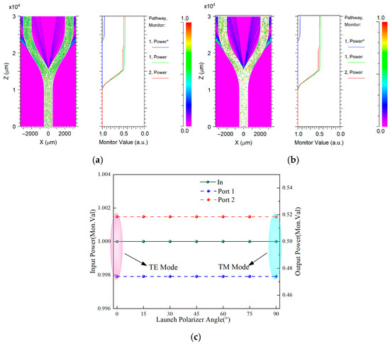
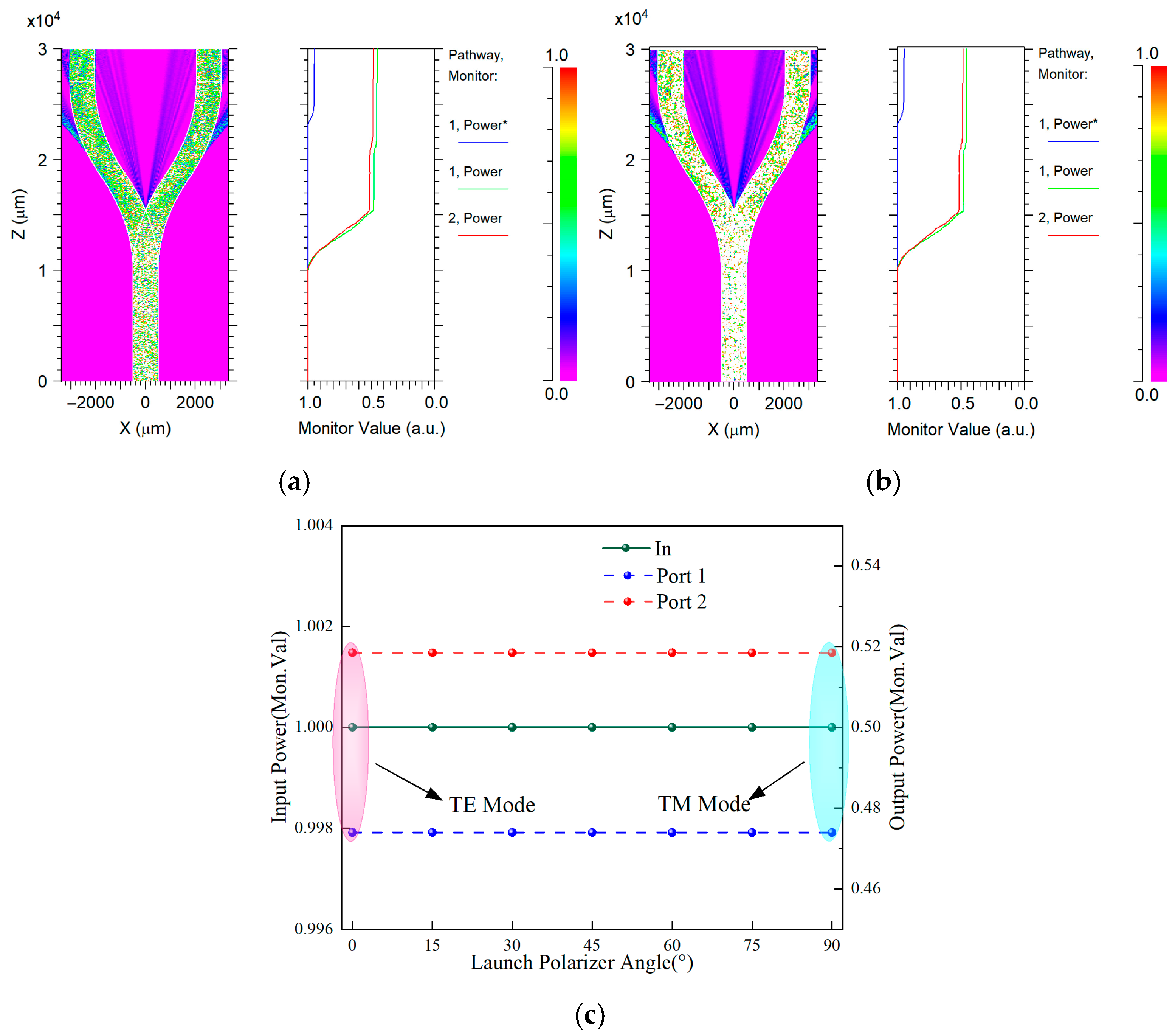
It should be noted that the above simulations are based on ideal structures and material parameters and do not consider the influence of actual manufacturing errors and multimode excitation conditions on the wavelength response. Therefore, to further evaluate the optical performance of the proposed 1 × 2 POF splitter under realistic multimode conditions, we performed multimode excitation simulations for both TE and TM polarizations, as shown in Figure 6. Unlike ideal single-mode or simplified scalar simulations, multimode simulations consider the coexistence and redistribution of multiple propagation modes within the large-core POF structure.
Figure 6.
Simulated output field distributions of the proposed splitter under (a) TE polarization and (b) TM polarization, and (c) the normalized output optical power as a function of the input polarization angle.
The simulation results show that some optical power leaks from the branch regions during propagation (Figure 6a,b). The reasons are mode redistribution, radiation loss at the Y-branch, and poor mode matching between the input waveguide and the two output branches. A drop in the normalized input and output power indicates that propagation loss exists inside the splitter. The simulation results for TE (Figure 6a) and TM (Figure 6b) polarizations give very similar normalized output power distributions. This means the 1 × 2 POF splitter structure has low dependence on polarization. We also simulated the normalized input and output power as a function of the input polarization angle (0°, 30°, 45°, 60°, and 90°). These results (as shown in Figure 6c) show that the normalized output power stays stable across this polarization range and there is no large variation. This further confirms that polarization-dependent loss is not a dominant loss mechanism in the proposed splitter.
In contrast, for large-core POF splitters, the main performance variations are closely related to multimode propagation, mode redistribution, junction radiation loss, and manufacturing-related geometric deviations [15,25,30]. The simulated splitting ratio under multimode excitation is approximately 47%:53%, slightly deviating from the ideal 50%:50% ratio. This result is reasonable because, in large-core multimode POF splitters, the output power distribution is strongly influenced by the mode composition and multimode interference within the splitting region. Constructive and destructive interference between different modes leads to a slight power imbalance between the two output ports [30,31,32].
Considering that the device is fabricated using a manual process, unavoidable deviations from the ideal symmetrical structure assumed in the simulations exist. Therefore, this study further conducted a sensitivity analysis on key structural parameters to quantitatively assess the impact of manufacturing errors on device performance. Using the optimized 17° branch angle and 17 mm bifurcation length as the initial values, we performed a parametric scan on the key geometric parameters.
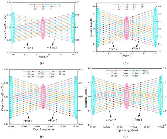
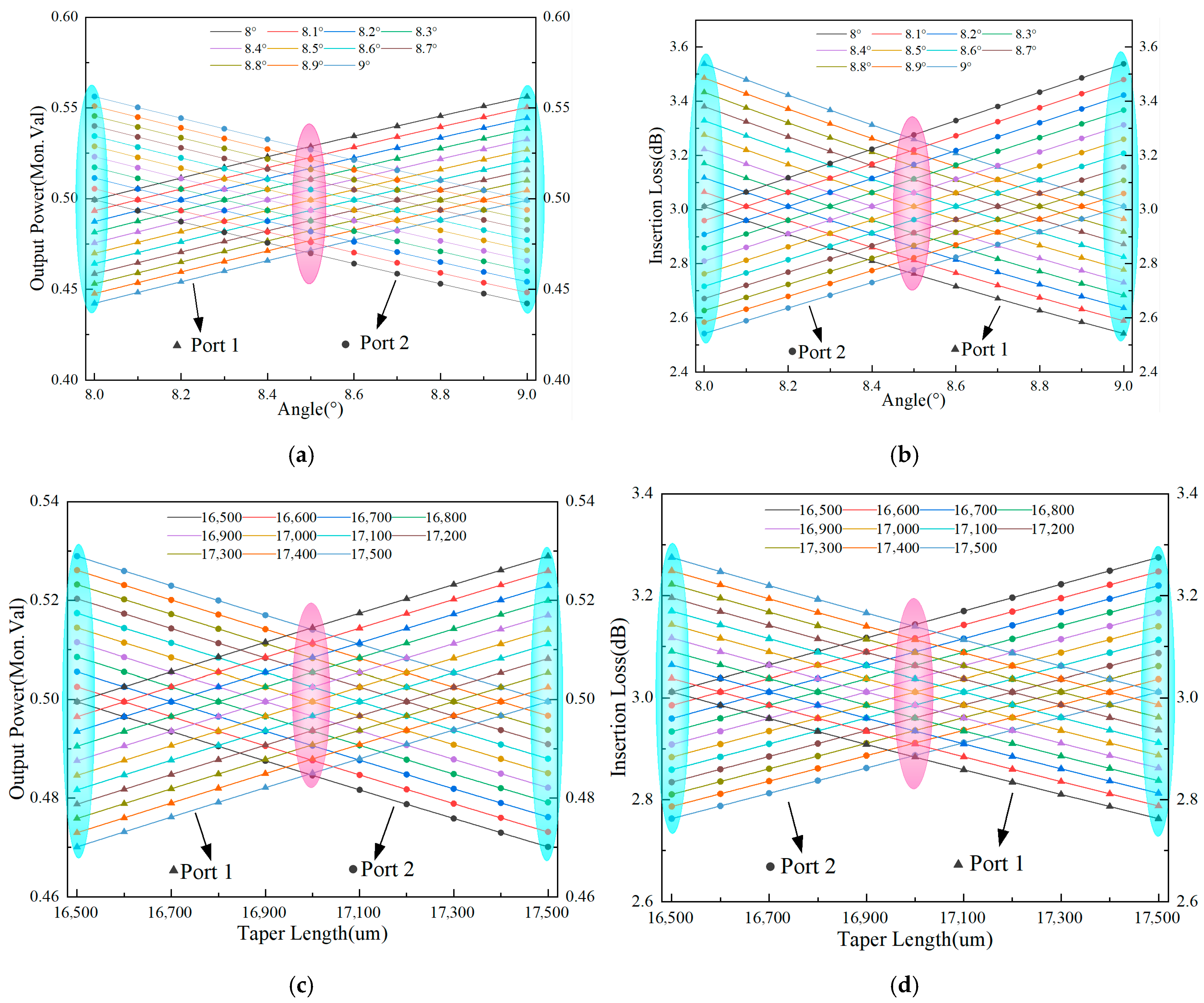
First, the two output branches were set at angles of ±8.5° relative to the input waveguide axis, and a deviation of ±0.5° per branch was introduced (i.e., a total branch angle variation within 17° ± 1°). We calculated the normalized optical power at the two output ports to obtain the insertion loss variation. The results show that the splitting ratio fluctuates between 44% and 56% when the branch angle changes within ±1°, indicating that the device is highly sensitive to the branch angle (Figure 7a). Compared with the theoretical insertion loss of an ideal 1 × 2 POF splitter (≈3.01 dB), the branch angle error introduces an additional loss of 0.55 dB (Figure 7b). In addition, we performed a sensitivity analysis on the bifurcation length over a range of ± 0.5 mm. The results show that the splitting ratio changes between 47% and 53% within this error range, indicating good symmetry preservation (Figure 7c). The corresponding insertion loss variation is shown in Figure 7d, with an additional loss of approximately 0.3 dB. Overall, the branch angle deviation has a greater impact on device performance than the bifurcation length deviation, primarily because the branch angle directly affects the energy distribution during mode splitting.
Figure 7.
Influence of branch angle deviation on (a) the output optical power and (b) the insertion loss variation, and influence of bifurcation length deviation on (c) the output optical power and (d) the insertion loss variation.
Based on the above analysis, as the deviation of key structural parameters decreases, the symmetry of the device is enhanced, the splitting uniformity improves, and the insertion loss decreases, as indicated by the red regions in Figure 7. In contrast, the blue regions at both ends (corresponding to larger deviations) show the opposite effect, i.e., reduced splitting uniformity and increased insertion loss.
4. Device Fabrication and Results
4.1. Device Fabrication
We fabricated a planar optical waveguide (POW) substrate with dimensions of 30 mm × 10 mm × 2 mm using injection molding, integrating a 1 × 2 Y-branch structure. The injection molding process ensured high dimensional consistency, making it suitable for mass production. Subsequent fiber coupling and encapsulation processes were performed manually under laboratory conditions. The specific manual fabrication procedure is described as follows.
Three PMMA POFs, each with a diameter of 1 mm and a length of 20 cm, were used as the input port and the two output ports, respectively. First, the fiber end faces were cut using a specialized POF cleaver. Subsequently, we performed progressive mechanical polishing using sandpaper with gradually decreasing grit sizes (800, 1500, and 3000 grit) to remove and reduce the surface defects and irregularities generated during the cutting process. After each polishing step, we observed the fiber end faces under an optical microscope (about 200× magnification) to check the surface quality. The final polished surfaces were smooth, without obvious scratches or edge chips.
We first inserted the polished POFs into the input and output slots of the PMMA waveguide substrate. All alignment steps were performed by hand. We then aligned the fiber end faces with the waveguide core region by moving the fiber position back and forth until the best alignment was found. Special care was taken to keep the two output fibers symmetric with respect to the Y-branch structure. We used transparent tape to hold the fibers in place, which kept the alignment stable during later processing.
A UV-curable adhesive (EPO-TEK OG603) was then injected into the tapered transition region between the fiber end faces and the waveguide slots. We used a microsyringe to inject and added the adhesive slowly in several small amounts to trap less air and form fewer bubbles. When no visible bubbles were observed, the filling process was considered complete. The device was then exposed to UV light for 20 min to ensure complete curing of the adhesive.
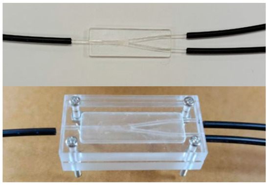
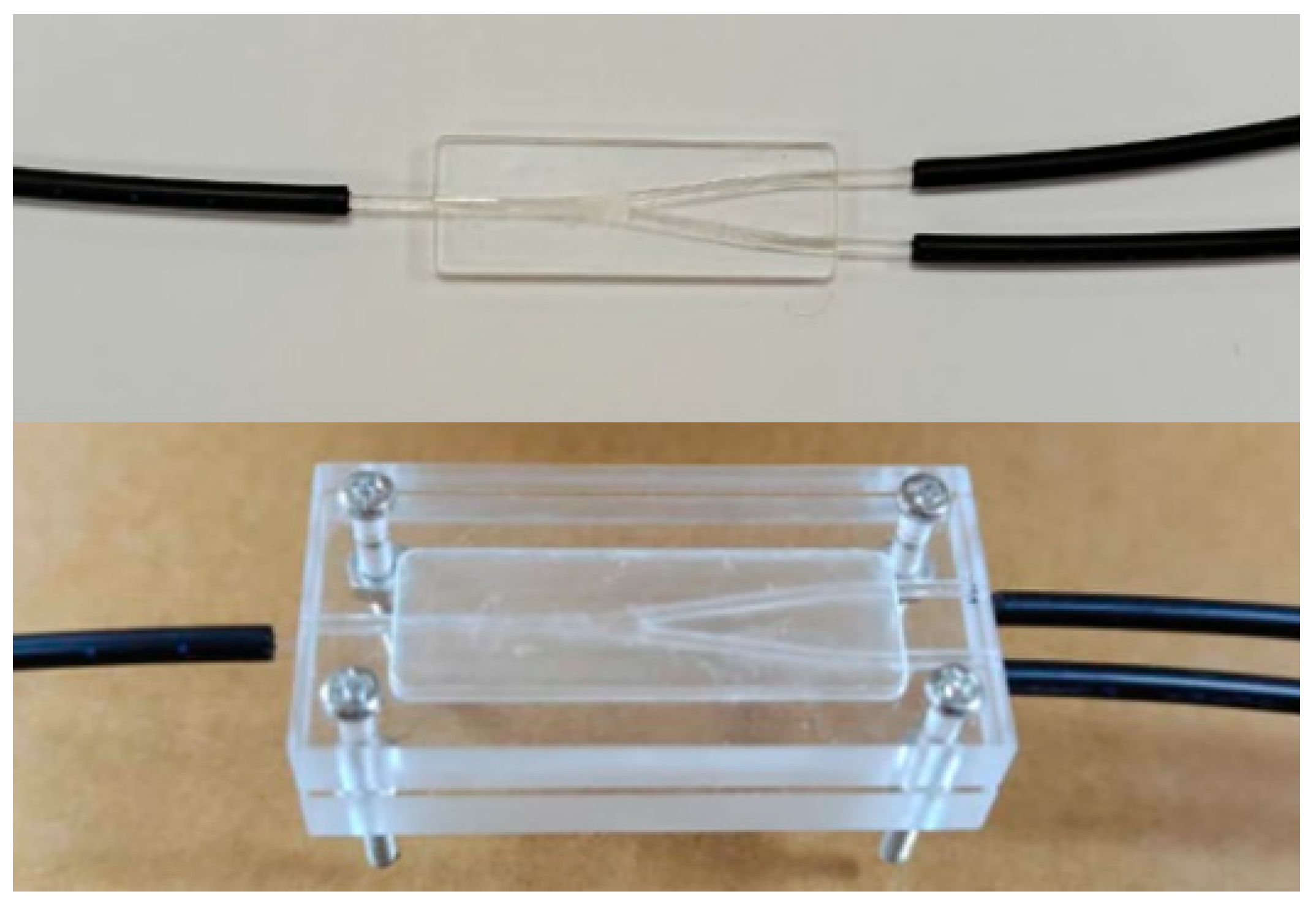
Finally, we used a PMMA cover plate to encapsulate the device, providing basic mechanical protection and preventing dust contamination. Figure 8 shows the fabricated splitter sample.
Figure 8.
Fabricated 1 × 2 POW splitters.
4.2. Measurement and Results
Ten POF splitter samples were manually fabricated in a laboratory environment. A 650 nm wavelength was selected as the test light source, and the optical power was measured using an OFT 820 optical loss meter (OPTOKON, Jihlava, Czech Republic). The light source was a 650 nm red LED operating in continuous wave (CW) mode for testing the POF in the visible light communication band. Light was directly injected into a 1 mm core diameter PMMA fiber using a butt-coupling method at the input end. The output optical power at each of the two branch ports was measured using an optical power meter. To eliminate additional losses introduced by connectors and patch cords, a 30 cm length of POF was used as a reference fiber (REF) before testing to correct subsequent measurement results. During testing, the two output ports of the splitter were connected to the optical power meter, and the optical power at each port was measured.
To improve the reliability and statistical significance of the measurement results and to quantitatively evaluate the repeatability and measurement stability of the manual fabrication process, we performed ten measurements on each sample under the same experimental conditions. Based on the collected data, the mean and standard deviation (SD) of the output optical power for each sample were calculated to assess the consistency between samples. The standard deviation was defined as follows:
where represents the optical power measured in the i-th experiment, represents the mean, and n = 10 represents the number of repeated measurements.
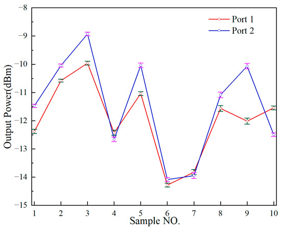
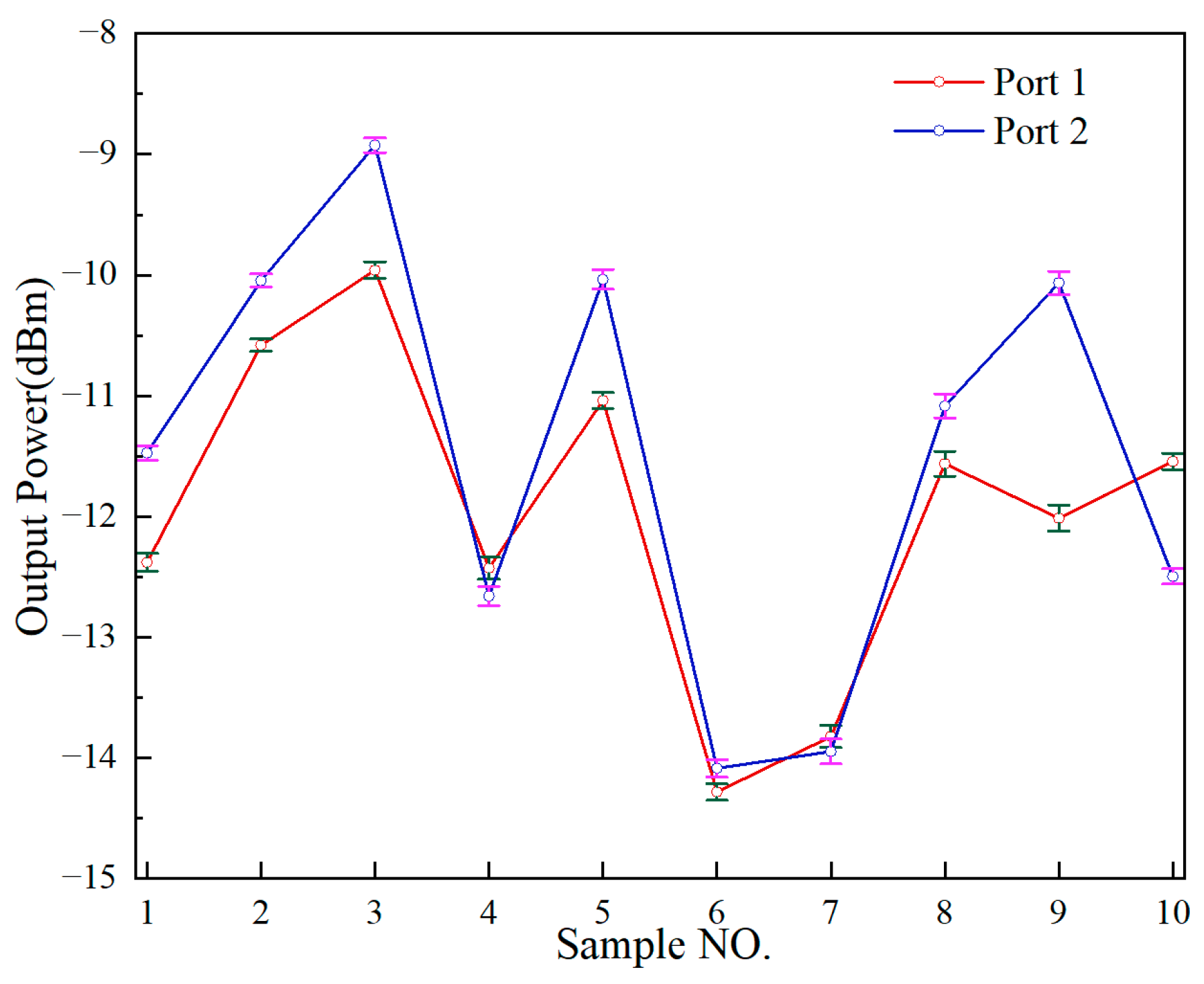
Figure 9 shows the statistical results of the output optical power of the ten fabricated samples at 650 nm wavelength for both ports. Each data point represents the mean of ten repeated measurements, and the error bars represent the corresponding standard deviations. The results show a significant imbalance between the two output ports, indicating sample-to-sample variations in the splitting performance. The observed standard deviation ranges from approximately ±0.05 to ±0.2 dBm, reflecting the presence of measurement fluctuations. These differences are mainly attributed to manufacturing tolerances introduced during manual alignment, polishing, and adhesive filling. Overall, this indicates that the device performance is significantly affected by manual fabrication errors, resulting in limited repeatability and consistency.
Figure 9.
Mean values and standard deviations of the output optical power for 10 fabricated samples measured under identical conditions.
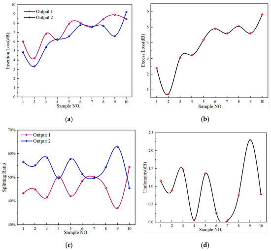
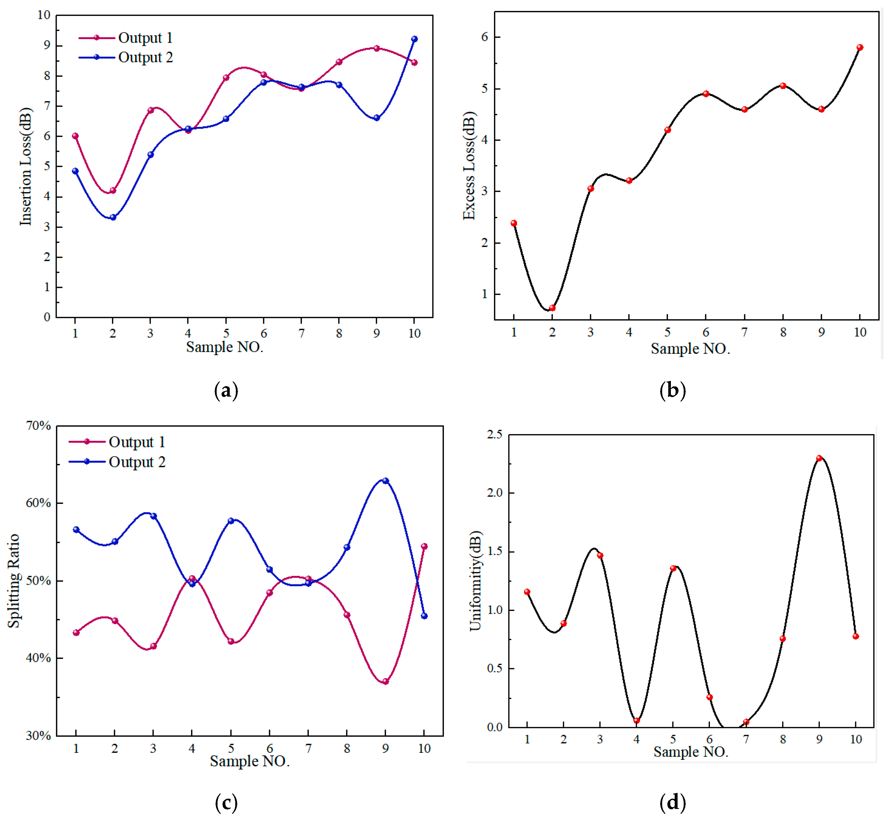
To characterize the device performance, the insertion loss, excess loss, splitting ratio, and splitting uniformity were calculated and statistically analyzed for the ten samples. The results show that the insertion loss ranges from 3.4 dB to 9.4 dB (Figure 10a), the excess loss ranges from 0.8 dB to 6 dB (Figure 10b), the splitting ratios range from 49.6%:50.4% to 37%:63% (Figure 10c), and the uniformity ranges from 0.06 dB to 2.4 dB (Figure 10d). These results indicate that the power difference between the two output ports is small and the splitting uniformity is satisfactory.
Figure 10.
The (a) insertion loss, (b) excess loss, (c) splitting ratio and (d) uniformity of POF splitters for 10 samples.
5. Discussion
This study designed and fabricated a 1 × 2 POF power divider using a laboratory-scale, manual fabrication process, independent of high-end or complex manufacturing equipment. This method offers advantages including low cost and ease of implementation; however, it inevitably introduces uncertainties during manufacturing.
First, with respect to fiber end-face quality, we employed a process of progressive hand polishing using successively finer sandpaper, followed by inspection under an optical microscope (approximately 200×). Nevertheless, the polishing process is operator-dependent and may leave residual microscopic roughness, and these surface defects introduce scattering loss, which represents a non-negligible loss mechanism in large-core multimode waveguides [26,27,28,29].
Regarding fiber alignment, the process is manual and lacks precise alignment steps. Although alignment is improved through iterative adjustments and temporary fixation, unavoidable axial misalignment and angular deviations remain. These deviations lead to incomplete mode coupling between the fiber and the waveguide, increasing insertion loss [26,28,30]. Therefore, alignment errors are considered one of the main factors affecting the consistency of device performance.
During the filling process of the UV-curable adhesive (EPO-TEK OG603), we used a microsyringe for slow injection to minimize air entrapment. However, residual microbubbles may still form in the absence of vacuum degassing or a controlled dispensing system. These microbubbles cause local refractive index discontinuities, leading to additional scattering and losses [19,21,25,32].
Furthermore, during UV curing, the refractive index of the adhesive increases from approximately 1.4734 to 1.5037, accompanied by approximately 1–4% volume shrinkage [11,18,19,21]. Owing to the geometric constraints and the relatively small adhesive volume, the resulting structural deformation is expected to be limited, while the increase in refractive index may partially enhance light confinement, thereby compensating for the small geometric perturbation [11,22,33]. Therefore, the effects of curing (including potential microbubble formation or adhesive inhomogeneity) are expected to be <0.001 dB and not a major source of loss.
Based on the simulation results presented in Section 3 and the above physical mechanism analysis, this paper establishes an error analysis model that decomposes the total loss into multiple contributing factors, including structural deviations, alignment errors, end face roughness, adhesive interface effects, bubble-induced scattering, and multimode excitation conditions. We summarized the loss range corresponding to each error factor, which is shown in Table 1. This model provides a quantitative explanation for the performance differences observed among the fabricated samples and highlights the inherent limitations of manual fabrication in terms of reproducibility.
Table 1.
The loss range corresponding to each error factor.
Despite these limitations, the fabrication method achieves a good balance between performance and complexity. To further evaluate the device performance, we selected five representative samples (Samples 1–5) that exhibited relatively low loss and good splitting uniformity for testing. Table 2 compares their insertion loss, excess loss, and splitting ratio with those of previously reported POF or polymer splitters at 650 nm. It should be noted that these samples represent the best performance achievable under the current fabrication conditions, not the average level. Our proposed 1 × 2 POF splitter achieves a low insertion loss (3.4–9.4 dB), a comparable excess loss (0.8–6 dB), and a near-ideal splitting ratio. Although some performance variation exists due to the manual fabrication process, the results show that competitive optical performance can be obtained with a simplified, low-cost approach. This makes the device a promising candidate for short-distance and cost-sensitive VLC applications.
Table 2.
Comparison of performance metrics of 1 × 2 splitters in other works and in this work at 650 nm.
This study shows good optical performance and a low-cost fabrication method, but some limitations still exist. Compared with conventional techniques like FBT and silica-based waveguides, our proposed method has an environmental advantage. This advantage comes from its simpler processing conditions, which include room-temperature UV curing and less material use [10,12]. However, we did not perform a quantitative assessment of energy consumption or chemical waste, nor did we conduct systematic environmental stability tests. In practical applications, the interfaces between the fiber, adhesive, and waveguide can be affected by changes in temperature and humidity. These changes can lead to shifts in refractive index, mismatch in thermal expansion, and mechanical stress, which could hurt long-term performance [19,21,28]. In addition, experimental validation has been performed only at one wavelength (650 nm) and on a small number of samples made by hand. No full study has been carried out on how the device behaves across different wavelengths in the whole POF working range, or on its long-term repeatability under environmental changes. Our future work will look at broadband testing, environmental reliability checks, and process optimization, including better alignment accuracy and adhesive control, so that device consistency can be improved and scalable fabrication can be achieved.
From the fabrication perspective, moving from current handmade prototypes to automated production with high yield brings many real-world challenges. These challenges include how to obtain precise and repeatable alignment between the fiber and waveguide, how to control the amount and spread of adhesive to avoid defects like voids or uneven thickness, and how to keep end-face quality consistent in large-scale production. Also, different variations caused by the process, such as curing shrinkage and thermal stress, must be controlled with care to ensure long-term reliability. To address these challenges, one needs to use precision alignment platforms, automated dispensing systems, and in-line inspection technologies. Process standardization and tolerance optimization are also needed [26,28,35,36].
6. Conclusions
We designed and experimentally demonstrated a low-cost 1 × 2 POF splitter based on POW. The device achieves efficient coupling using a large-core (1 mm) POF, enabling effective multimode transmission in the visible light band. We optimized the Y-branch structure using BPM, resulting in a near-balanced splitting ratio and low theoretical excess loss.
The device was fabricated on an injection-molded PMMA substrate using manual fiber insertion and UV-cured adhesive filling. Experimental results at 650 nm show an insertion loss ranging from 3.4 to 9.4 dB and an excess loss from 0.8 to 6 dB. Statistical analysis indicates that, despite performance variations arising from fabrication tolerances, the device maintains stable operation under laboratory conditions. Furthermore, we quantified the influence of alignment errors, end-face roughness, adhesive interface effects, and microbubbles on the total loss based on loss mechanism analysis and simulation. Despite these limitations, the device exhibits low polarization sensitivity and stable performance under multimode conditions, demonstrating its suitability for short-range VLC applications.
In addition, our proposed Y-branch waveguide architecture can be extended to 1 × N splitters through cascading or tree-structured configurations. However, such scaling introduces challenges, including accumulated excess loss, increased sensitivity to structural asymmetry, and enhanced multimode interference. Consequently, careful optimization of branch angles, transition lengths, and geometric symmetry is required to maintain uniform power distribution. For higher-order splitters, advanced design strategies, such as adiabatic transitions and multi-stage loss balancing, may be necessary to achieve acceptable performance.
In summary, the proposed approach provides a feasible route toward low-cost optical power distribution devices while identifying key factors affecting performance and scalability. Future work will focus on process automation, evaluation of broadband and environmental stability, and the development of scalable splitter architectures for emerging VLC and short-range optical interconnect applications.
Author Contributions
Conceptualization, X.D.; methodology, M.S.A.-R. and X.D.; software, X.D.; validation, X.D.; formal analysis, X.D.; investigation, X.D.; resources, M.S.A.-R.; data curation, X.D.; writing—original draft preparation, X.D.; writing—review and editing, M.S.A.-R.; visualization, X.D. and M.S.A.-R.; supervision, M.S.A.-R.; project administration, X.D. and M.S.A.-R.; funding acquisition, X.D. and M.S.A.-R. All authors have read and agreed to the published version of the manuscript.
Funding
This research was funded by Dezhou Big Data and Intelligent Sensing Technology Engineering Research Center (project No. PT2025KJX002).
Institutional Review Board Statement
Not applicable.
Informed Consent Statement
Not applicable.
Data Availability Statement
The original contributions presented in this study are included in the article. Further inquiries can be directed to the corresponding author.
Acknowledgments
This research was conducted in the Broadband, Network & Security Laboratory, Universiti Kebangsaan Malaysia (UKM).
Conflicts of Interest
The authors declare no conflicts of interest.
References
- Ab-Rahman, M.S.B.; Mohamed, I.M.M. Options and Challenges in Next-Generation Optical Access Networks (NG-OANs). OPTIK 2015, 126, 131–138. [Google Scholar]
- Azizan, L.A.-H.; Ab-Rahman, M.S.; Jumari, K. Analytical approach on SNR performance of visible light communication for modern lighting layout. In Proceedings of the 2012 International Conference on Innovation Management and Technology Research, Malacca, Malaysia, 21–22 May 2012; pp. 332–336. [Google Scholar]
- Ng, B.; Ab-Rahman, M.S.; Premadi, A. Development of monitoring system for FTTH-PON Using Combined ACS and SANTAD. Int. J. Commun. Syst. 2010, 23, 429–446. [Google Scholar] [CrossRef] [Scilit]
- Ab-Rahman, M.S.; Ng, B.; Aziz, S.A.C.; Mastang Premadi, A.; Saupe, M.N.M.; Jumari, K. High Efficiency of FTTH Network Management through SANTAD. J. Netw. Syst. Manag. 2010, 18, 210–231. [Google Scholar]
- Zadobrischi, E. Traffic and Vehicle Management in Roundabouts Through Systems Based on Dedicated Short-Range Communications and Visible Light Communications. Electronics 2025, 14, 317. [Google Scholar] [CrossRef] [Scilit]
- Schrenk, B. Wideband FTTR PON integrating optical wireless access. In Proceedings of the 2024 Optical Fiber Communications Conference and Exhibition (OFC), San Diego, CA, USA, 24–28 March 2024; IEEE: New York, NY, USA, 2020; pp. 1–3. [Google Scholar]
- Teng, C.; Deng, H.; Liu, H.; Yang, H.; Yuan, L.; Zheng, J.; Deng, S. Refractive Index Sensor Based on Twisted Tapered Plastic Optical Fibers. Photonics 2019, 6, 40. [Google Scholar] [CrossRef] [Scilit]
- Manea, H.K.; Molood, Y.N.; Al-Jubouri, Q.; Taha, B.A.; Chaudhary, V.; Rustagi, S.; Arsad, N. A comparative study of plastic and glass optical fibers for reliable home networking. ECS J. Solid State Sci. Technol. 2023, 12, 057003. [Google Scholar] [CrossRef] [Scilit]
- Ni, Z.; Takizawa, T.; Terasawa, H.; Sugihara, O. Flexible self-written optical waveguides using plastic optical fibers for automotive applications. Opt. Eng. 2025, 64, 087104. [Google Scholar] [CrossRef] [Scilit]
- Ab-Rahman, M.S.; Safnal, H.; Kaharudin, I.H.; Hwang, I.-S. Green Technology Solution for Small-World Communication Using Plastic Optical Fiber (POF) and Light Emitting Diode (LED)—Design and Application. Sustainability 2022, 14, 10894. [Google Scholar] [CrossRef] [Scilit]
- Liu, T.; Wang, S. Epoxy resin multimode optical waveguide fabricated by non-contact photolithography. Opt. Commun. 2024, 569, 130840. [Google Scholar] [CrossRef] [Scilit]
- Xu, X.; Lu, X.; Pang, F.; Chen, N.; Wei, H.; Zhang, L.; Zhang, Q.; Wang, T. Overcoming oxygen inhibition in UV photolithography for the fabrication of low-loss polymer waveguides. Opt. Lett. 2024, 49, 2369–2372. [Google Scholar] [CrossRef] [Scilit]
- Cairone, F.; Gallo Afflitto, F.; Stella, G.; Cicala, G.; Ashour, M.; Kersaudy-Kerhoas, M.; Bucolo, M. Micro-Optical Waveguides Realization by Low-Cost Technologies. Micro 2022, 2, 123–136. [Google Scholar] [CrossRef] [Scilit]
- Koike, Y. Plastic Optical Fibers. In Springer Handbook of Functional Polymers; Springer Nature: Singapore, 2026; pp. 529–541. [Google Scholar]
- Yau, I.; Sani, S.M.; Usman, A.D.; Tekanyi, A.M.; Abba, A.M.; Gambo, D. Enhancing the Transmission Performance of Step Index Plastic Optical Fiber. In Proceedings of the 2022 5th Information Technology for Education and Development (ITED), Abuja, Nigeria, 1–3 November 2022; IEEE: New York, NY, USA, 2022; pp. 1–5. [Google Scholar]
- Lanziano, L.; Sherf, I.; Malka, D. A 1 × 8 Optical Splitter Based on Polycarbonate Multicore Polymer Optical Fibers. Sensors 2024, 24, 5063. [Google Scholar] [CrossRef] [Scilit]
- Ghazali, M.S.; Romlay, F.R.; Ehsan, A.A. Development of Polymer-Based Y-Branch Symmetric Waveguide Coupler Using Soft Lithography Technique. In Recent Trends in Mechatronics Towards Industry 4.0: Selected Articles from iM3F 2020, Malaysia, 16 July 2021; Springer: Singapore, 2021; pp. 71–76. [Google Scholar]
- Wei-Hung, S.; Guo, H.-J.; Hsu, K.-D. Fabrication of the PMMA photopolymer for holographic inscription with the wavelength of 633nm. In Photonic Fiber and Crystal Devices: Advances in Materials and Innovations in Device Applications XIX; SPIE: Bellingham, WA, USA, 2025; Volume 13608. [Google Scholar]
- Yulianti, I.; Insan, S.M.K.; Putra, N.M.D.; Purwinarko, A.; Widiarti, N.; Ngajikin, N.H. Thermal Durability Characterization of a Simple Polymethyl-methacrylate (PMMA) Based-Optical Waveguide. J. Penelit. Fis. Dan Apl. 2024, 14, 113–124. [Google Scholar] [CrossRef] [Scilit]
- Mizuno, Y.; Theodosiou, A.; Kalli, K.; Liehr, S.; Lee, H.; Nakamura, K. Distributed polymer optical fiber sensors: A review and outlook. Photon. Res. 2021, 9, 1719–1733. [Google Scholar] [CrossRef] [Scilit]
- Mohammad-Reza, A.; Hassanpour, A. UV-curable polymer nanocomposites: Material selection, formulations, and recent advances. J. Compos. Sci. 2024, 8, 441. [Google Scholar] [CrossRef] [Scilit]
- Prajzler, V.; Maštera, R.; Špirková, J.; Jeřábek, V. Compact multimode polymer optical 1 × 2 Y splitters with large core planar waveguide. J. Opt. 2014, 43, 310–316. [Google Scholar] [CrossRef] [Scilit]
- Serecunova, S.; Seyringer, D.; Pudis, D.; Mizera, T.; Uherek, F.; Seyringer, H. Design and simulation of 3D 1 × 4 multimode interference splitter. In Proceedings of the 2022 International Conference on Broadband Communications for Next Generation Networks and Multimedia Applications (CoBCom), Graz, Austria, 12–14 July 2022; IEEE: New York, NY, USA, 2022. [Google Scholar]
- Lalin, N.S.; Nijhum, Z.T.; Amina, M.N.; Monira, S.; Malakar, T.; Rasel, M.O.; Sikder, M.S. Optimization and Performance Analysis of 1× 2 and 1× 4 MMI Splitters on a Polymer Platform for Board-Level Optical Interconnects. 2026. Available online: https://www.researchsquare.com/article/rs-8847414/v1 (accessed on 6 May 2026).
- Tasnim, F.; Afsary, N.; Rasel, O.F.; Ishigure, T. Graded-index core-based polarization beam splitters realized with symmetric polymer directional couplers. Opt. Contin. 2023, 2, 1040–1052. [Google Scholar] [CrossRef] [Scilit]
- Ghazali, M.S.; Romlay, F.R.; Ehsan, A.A. Manufacturing of Polymer-based 1 × 2 Y-branch Symmetric and Asymmetric Waveguide Coupler through Moulding Technique. Int. J. Automot. Mech. Eng. 2021, 18, 8998–9005. [Google Scholar] [CrossRef] [Scilit]
- Ab-Rahman, M.S.; Guna, H.; Arsad, N. Effect of the Surface Roughness on Cross Sectional Properties of 1 × 3 Polymer Optical Fiber-based Splitter. J. Phys. Conf. Ser. 2021, 1748, 062008. [Google Scholar] [CrossRef] [Scilit]
- Cezar, F.C.S.; Morales-Alvarado, C.E.; Volpato, N.; Macedo, A.G.; Rodrigues, P.C.; Pohl, A.D.A.P. Fabrication of Y-Branch Power Splitters using Additive Manufacturing. In Proceedings of the 2024 24th International Conference on Transparent Optical Networks (ICTON), Bari, Italy, 14–18 July 2024; IEEE: New York, NY, USA, 2024; pp. 1–4. [Google Scholar] [CrossRef] [Scilit]
- Supian, L.S.; Ab-Rahman, M.S.; Arsad, N.; Guna, H.; Ismail, K. Polymer Optical Fiber Splitter Using Tapered Techniques for. Green Comput. Technol. Comput. Ind. 2021, 2021, 55. [Google Scholar]
- Savović, S.; Djordjevich, A.; Savović, I.; Min, R. Mode Coupling and Steady-State Distribution in Multimode Step-Index Organic Glass-Clad PMMA Fibers. Photonics 2022, 9, 297. [Google Scholar] [CrossRef] [Scilit]
- Richards, D.; Lopez, A.; Losada, M.A.; Mena, P.V.; Ghillino, E.; Mateo, J.; Antoniades, N.; Jiang, X. Overcoming Challenges in Large-Core SI-POF-Based System-Level Modeling and Simulation. Photonics 2019, 6, 88. [Google Scholar] [CrossRef] [Scilit]
- Prajzler, V.; Mastera, R.; Knietel, M. Filter embedded optical planar splitter connectable to large core plastic optical fibers. In Proceedings of the 2017 Opto-Electronics and Communications Conference (OECC) and Photonics Global Conference (PGC), Singapore, 31 July–4 August 2017; IEEE: New York, NY, USA, 2017; pp. 1–2. [Google Scholar]
- Sariki, R.K.; Kambavalasa, S.K.; Bandari, N.K.; Moningi, R.K. Design and fabrication of POF Couplers/Splitters for Networking and Displacement Sensing. In Proceedings of the 2021 International Symposium of Asian Control Association on Intelligent Robotics and Industrial Automation (IRIA), Farmagudi, India, 20–22 September 2021; IEEE: New York, NY, USA, 2021; pp. 183–186. [Google Scholar]
- Prajzler, V.; Knietel, M.; Maštera, R. Large core optical planar splitter for visible and infrared region. Opt. Quantum Electron. 2016, 48, 155. [Google Scholar] [CrossRef] [Scilit]
- Yulianti, I.; Astuti, B.; Alauhdin, M.; Idrus, S.M.; Noor, M.Y.M.; Mufatihah, N.; Aji, M.P.; Putra, N.M.D.; Anggaladewi, S.Y.; Leonardy, J. Fabrication and characterization of low-cost optical waveguides using recycled expanded polystyrene (EPS) as core material. Results Opt. 2025, 22, 100947. [Google Scholar] [CrossRef] [Scilit]
- Zheng, L.; Keppler, N.; Zhang, H.; Behrens, P.; Roth, B. Planar Polymer Optical Waveguide with Metal—Organic Framework Coating for Carbon Dioxide Sensing. Adv. Mater. Technol. 2022, 7, 2200395. [Google Scholar] [CrossRef] [Scilit]

Disclaimer/Publisher’s Note: The statements, opinions and data contained in all publications are solely those of the individual author(s) and contributor(s) and not of MDPI and/or the editor(s). MDPI and/or the editor(s) disclaim responsibility for any injury to people or property resulting from any ideas, methods, instructions or products referred to in the content. |
© 2026 by the authors. Licensee MDPI, Basel, Switzerland. This article is an open access article distributed under the terms and conditions of the Creative Commons Attribution (CC BY) license.