


Abstract
With the advent of 6G mobile communication, the demand for ultra-high bandwidth wireless communication has increased rapidly, drawing significant attention to visible light communication (VLC) as a promising emerging technology. GaN-based laser diodes (LDs) are regarded as high-speed light sources for VLC owing to their high modulation bandwidth and high optical power density. Apart from the active region design, the LD’s structure also plays a crucial role in determining their dynamic properties, which have yet to be thoroughly studied in III-nitride LDs. In this work, we systematically investigate InGaN/GaN laser diodes with three ridge waveguide configurations: a conventional single-ridge structure, a dual-ridge large-mesa structure, and a dual-ridge small-mesa structure. The threshold current, small-signal modulation bandwidth of devices with different structures are comparatively analyzed. Experimental results reveal that the double-ridge small mesa laser diode achieves a modulation bandwidth of −3 dB at 6.02 GHz. These results provide valuable insights into the structural optimization of GaN-based high-speed laser diodes and offer practical guidance for the development of high-performance, energy-efficient VLC transmitters.
1. Introduction
GaN-based light-emitting diodes (LEDs) have fundamentally transformed conventional lighting technologies and driven the rapid development of solid-state lighting systems [1,2]. In the past decade, high-efficient blue LEDs have also been explored as optical transmitters for visible light communication (VLC) and underwater wireless optical communication (UWOC) [3,4,5,6]. However, the modulation bandwidth of LEDs is fundamentally limited by their relatively long carrier lifetime, which restricts achievable data rates and hinders their application in ultra-high-speed communication scenarios [7]. Laser diode (LD)-based VLC systems have recently been developed as a promising alternative for realizing compact, droop-free, and high-speed optical data links [8]. Benefiting from a significantly shorter photon lifetime, GaN-based LDs can support multi-gigahertz modulation bandwidths, making them ideal candidates for high-speed LiFi networks, intersatellite communication, and optical interconnects [9]. In this context, GaN-based blue laser diodes are particularly promising for high-speed VLC owing to their compatibility with existing lighting infrastructure and their capability for ultra-fast modulation [10].
Since the initial development of practical blue LD in 1997, advances in GaN growth and p-type doping have significantly improved the reliability of GaN-based lasers, with the output power of individual diodes increasing from a few milliwatts to several watts [11]. GaN-based lasers have been widely applied in optical storage [12], biomedical applications [13], and lighting and display [14]. However, high-speed blue lasers for VLC systems have not been extensively explored. The modulation bandwidth of several commercial blue laser diodes is typically ~1 GHz, which is substantially lower than that of InP- and GaAs-based near-infrared lasers [15,16,17,18]. To overcome bandwidth limitations, researchers have optimized the structure and device size of GaN LDs. In 2013, Scott Watson et al. designed a laser with a modulation bandwidth of 1.4 GHz using TO packaging [19]. In 2015, Yu-Chieh Chi et al. optimized the design and used TO-38 packaged GaN blue LD. Through throughput intensity optimization, the OFDM encoding bandwidth can be extended to 1.5 GHz [20]. In 2016, Changmin Lee et al. studied the dynamic characteristics of a group-III nitride multi-quantum-well LD emitting at 410 nm. The laser was grown on a semi-polar GaN substrate, and the 5 GHz modulation bandwidth was experimentally verified [21]. In 2022, Stephen P. Najda et al. designed an AlGaInN laser diode and achieved a high bandwidth of 1.38 GHz in a 10 m-long plastic optical fiber [22].
Various approaches have been explored to achieve high-speed GaN-based laser diodes, with active region engineering and device structure being key factors in enhancing modulation bandwidth. Techniques such as quantum dots can increase carrier–photon interaction and differential gain [23], while Bragg gratings in ridge waveguides improve mode stability and modulation response [24]. Semi-polar quantum wells can suppress the quantum-confined Stark effect and enhance recombination efficiency, though high-quality growth on c-plane substrates remains challenging [25]. Nevertheless, challenges such as the high cost of substrates and the immaturity of material growth techniques remain. Therefore, the design and fabrication of GaN-based laser diodes on c-plane substrates remain critically important for advancing high-speed applications. Recently, our group has been developing c-plane GaN-based high-speed mini-LD and micro-LD, which exhibit improved dynamic performance, as the ridge width and cavity length strongly influence the modulation characteristics of laser diodes [26]. In 2024, Sun et al. achieved a modulation bandwidth of 4.47 GHz by adjusting the design parameters of key research devices, including cavity length, quantum well thickness, ridge waveguide width, and PN junction spacing [27]. In the same year, Wang et al. developed an InGaN/GaN quantum well mini-laser diode (mini-LD) with a modulation bandwidth of 5.9 GHz [28]. In 2025, Jia et al. added a trapezoidal electron-blocking layer (EBL) and an unintentional doping layer near the quantum line, and measured a large modulation bandwidth of 7.8 GHz for their designed 500 μm-long cavity laser [29]. In 2026, Hu et al. designed a blue mini-LD with a bandwidth of 8.4 GHz by improving the carrier transport rate and the uniform distribution of the active region [30].
Building on these insights, the device structure design will be another important factor that may affect the dynamic properties of GaN-based LDs. In this work, the design and fabrication of short-cavity, dual-ridge GaN-based laser diodes are experimentally investigated, which represent a promising strategy to achieve higher modulation bandwidths. Three different laser diode configurations are considered, and a series of devices is fabricated and characterized. A −3 dB modulation bandwidth of 6.02 GHz is achieved with a threshold current of 65 mA. The experimental results provide in-depth insights into the influence of device structural design on modulation bandwidth and highlight the advantages of device miniaturization in nitride-based laser diodes.
2. Design and Fabrication
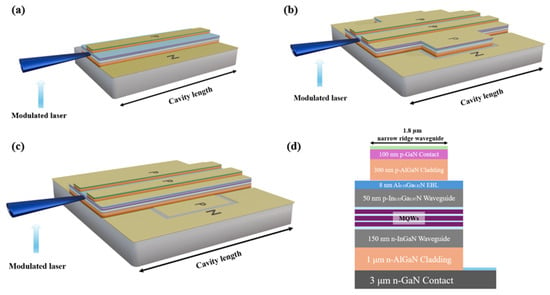
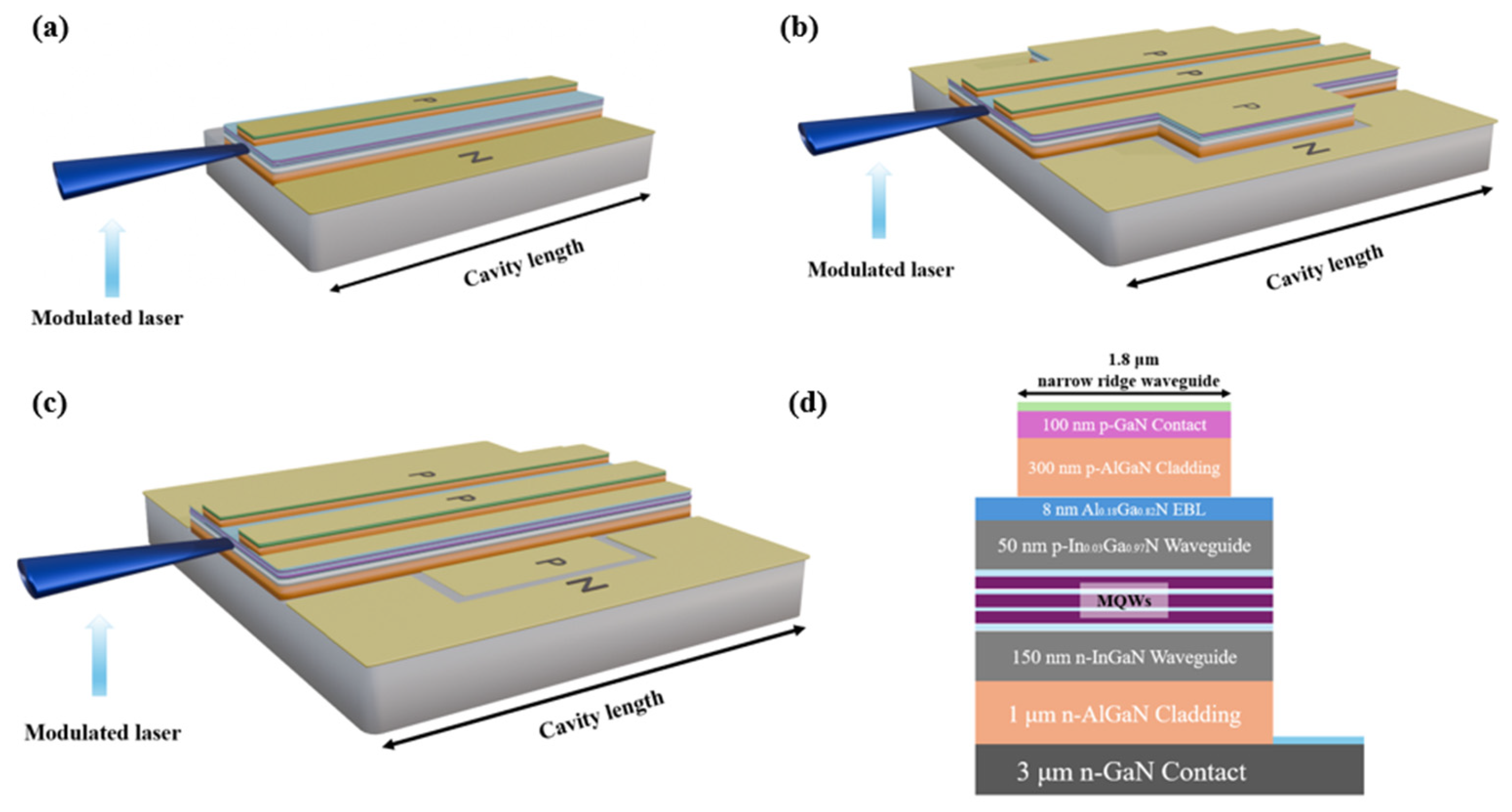
We designed three laser diode structures. Figure 1 illustrates the 3D structure of the LDs. The devices are grown on a c-plane (0001) GaN substrate using the metal–organic chemical vapor deposition (MOCVD) technique. Figure 1a shows the conventional single-ridge waveguide laser diode, in which current injection and optical confinement are defined by a single ridge structure along the cavity length. Figure 1b and c present two types of dual-ridge laser diodes, namely the dual-ridge large-mesa structure and the dual-ridge small-mesa structure, respectively. In the dual-ridge configurations, an additional ridge is introduced to further tailor the current distribution and optical mode confinement. Compared with the single-ridge structure, the dual-ridge large-mesa structure provides enhanced lateral current spreading control while maintaining a relatively large current-injection area, which can influence carrier distribution and parasitic capacitance. In contrast, the dual-ridge small-mesa structure further reduces the effective injection area and mesa size, leading to stronger current confinement, a smaller effective mode volume, and potentially reduced parasitic resistance–capacitance (RC) effects. As a result, the dual-ridge small-mesa design is expected to exhibit improved high-frequency modulation performance compared with both the single-ridge and dual-ridge large-mesa structures. For convenience, the three laser diode structures are hereafter denoted as SR-LD, DR-LD, and DR-mini-LD, corresponding to the single-ridge, dual-ridge large-mesa, and dual-ridge small-mesa designs, respectively. If a numerical value follows the device abbreviation, it indicates the cavity length of the corresponding laser diode, expressed in micrometers.
Figure 1.
Structural comparison of GaN-based laser diodes with different ridge and mesa configurations. (a) SR-LD. (b) DR-LD. (c) DR-mini-LD. (d) Common epitaxial layer structure shared by all devices.
Although the three laser diode structures differ in ridge geometry and mesa size, they share the same epitaxial layer structure, as illustrated in Figure 1d. The epitaxial structure consists of a 3 μm Si-doped n-GaN contact layer ([Si] = 2 × 1018 cm−3), a 1 μm n- cladding layer ([Si] = 3 × 1018 cm−3)), and a 150 nm n- waveguide layer ([Si] = 2 × 1018 cm−3)). The active region consists of three 3 nm quantum wells (QW) separated by three 5 nm quantum barriers, followed by a 50 nm p- waveguide layer. Then, an 8 nm Mg doped electron blocking layer (EBL) is grown on the topside ([Mg] = 5 × 1018 cm−3)) followed by a 0.3 μm p- cladding layer. Then followed by a 0.1 μm highly doped p-GaN contact layer with a doping concentration of 1 × 1019 cm−3) optimized to reduce the series resistance ([Mg] = 1 × 1019 cm−3)) for high-speed operation. This design ensures that the observed differences in device performance can be primarily attributed to structural effects rather than variations in material composition.
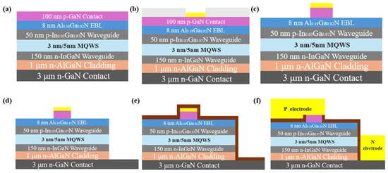
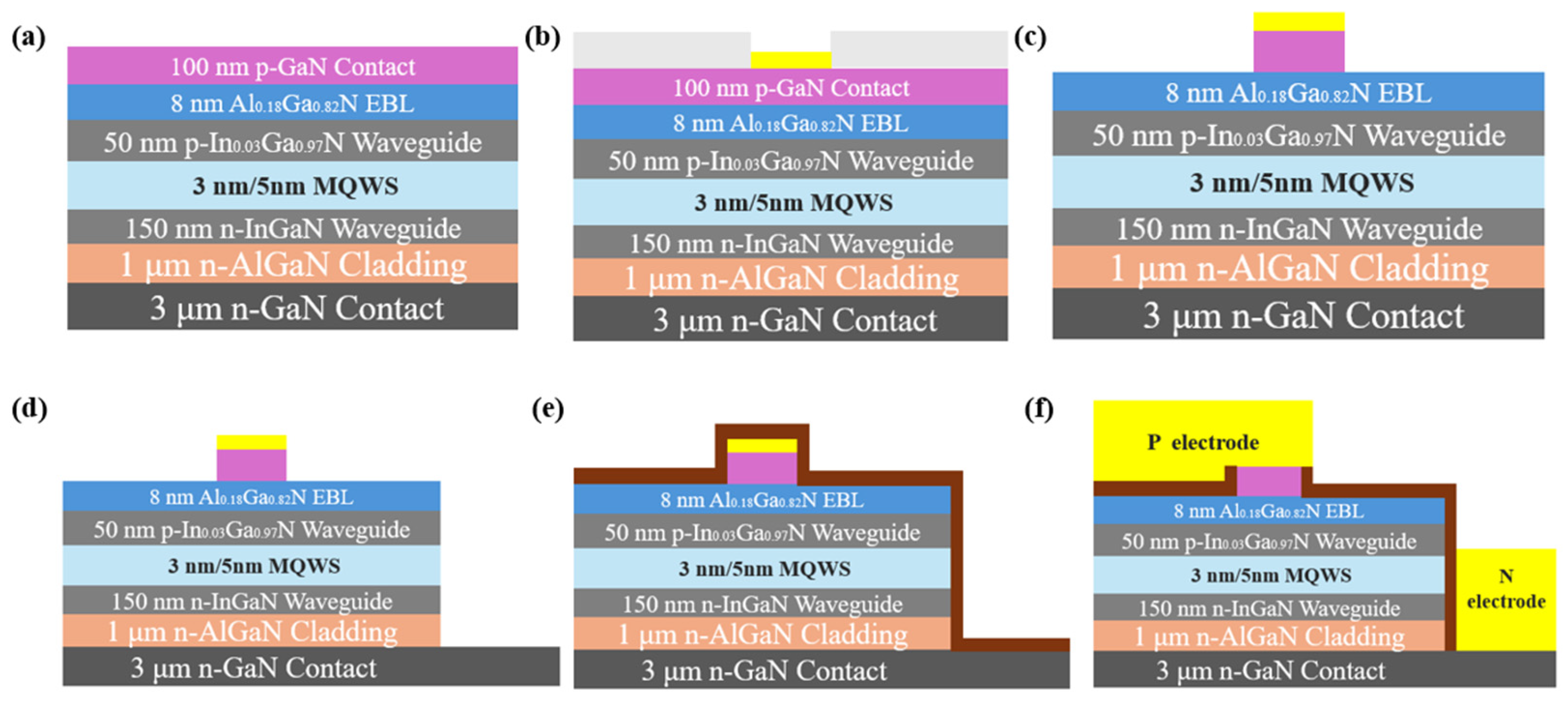
The fabrication process of laser diodes is schematically illustrated in Figure 2. First, epitaxial layers are grown on the substrate to form the active region, including the quantum wells, and the waveguide structure. Photolithography is then used to define the ridge patterns, followed by ridge etching to form the waveguide structures. A dielectric layer is subsequently deposited for electrical isolation. P-type contact electrodes are formed and annealed to achieve low-resistance ohmic contacts. After that, the N-type electrode regions are etched, and SiO2 passivation as well as oxide layer etching are performed to protect the waveguide and suppress surface leakage. Finally, metal electrodes are deposited to complete the p- and n-type contacts, and the devices are cleaved to form laser cavities. This fabrication sequence ensures well-defined optical waveguide structures and reliable electrical contacts, providing a foundation for the stable operation of high-performance GaN-based laser diodes.
Figure 2.
Schematic illustration of the key fabrication steps of the laser diodes: (a) Epitaxial layers growth. (b) Formation of the p-type contact electrode. (c) Ridge etching to define the waveguide structure. (d) Etching for n-type electrode formation. (e) SiO2 passivation; (f) Oxide opening followed by metal electrode deposition.
A dynamic response model was developed to investigate the influence of the active region on the modulation of bandwidth. The transfer function can be derived from the carrier–photon rate equations and is expressed as [28]:
The relaxation resonance frequency provides an intuitive measure of the laser’s high-speed modulation capability. The damping coefficient is given by , where is a constant that quantifies the strength of the damping effect.
We further examine the dependence of the resonance frequency on the current injection [28]:
To characterize the differential gain of the laser, we investigated the relationship between the and the square root of the normalized injection current, . Here, is the injection current, is the threshold current, is the optical confinement factor, is the group velocity, is the differential gain, is the elementary charge, is the volume of the active region, and is the injection efficiency. Above threshold, the square root of the driving current is proportional to the .
In this study, three different laser diode structures with varying cavity lengths were considered, and a total of five devices were fabricated and characterized. The performance of these laser diodes was experimentally evaluated under different injection currents.
3. Results and Discussions
The light output power-injection current and current–voltage (L–I–V) characteristics were measured using a custom-built LD characterization system, from which the threshold currents of all samples were extracted.
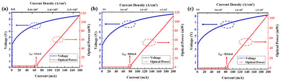
Figure 3 shows the L–I–V performance of the LDs. A Keithley 2450 (Tektronix, Keithley 2450, Cleveland, OH, USA) source-measure unit was used as the pulsed current source. The received optical signal was detected using a Newport 2936-R optical power meter (Newport, 2936-R, Irvine, CA, USA) equipped with a calibrated 818-SL silicon photodetector (Newport, 818-SL, Irvine, CA, USA). In our experiments, the laser diodes were driven with pulsed current of 100 μs pulse width and 1 ms delay, corresponding to a duty cycle of approximately 9.1%. The current measurement step was 1 mA. The three laser structures exhibit clear differences in their threshold currents and slope efficiencies. The DR-mini-LD shows the lowest threshold current of 65 mA and the highest slope efficiency of 1.026 W/A. This is mainly due to its small-aperture double-ridge design, which provides strong current confinement and high overlap between the optical mode and the active region, leading to efficient carrier injection and reduced non-radiative losses. In contrast, the DR-LD has a higher threshold current of 80 mA and a lower slope efficiency of 0.916 W/A. While it still benefits from a double-ridge structure, the larger ridge width slightly reduces the current confinement, resulting in a modest increase in threshold and a slight decrease in slope efficiency. The SR-LD device exhibits the highest threshold current of 82 mA and the lowest slope efficiency of 0.895 W/A. In this case, the absence of lateral confinement leads to significant current spreading and less effective carrier utilization, which increases the threshold and reduces efficiency. Above threshold, the output power increases nearly linearly with injection current, indicating stable lasing and good current-to-light conversion efficiency over the measured current range.
Figure 3.
(a) Light output power vs. injection current vs. voltage (L–I–V) characteristics of the DR-mini-LD. The blue line represents voltage, and the red line represents optical power. (b) L–I–V characteristics of the DR-LD. (c) L–I–V characteristics of the SR-LD.
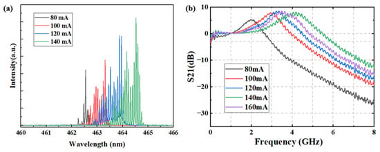
The electroluminescence (EL) spectra of the DR-mini-LD were measured under different injection currents using an optical spectrometer (Thorlabs, OSA201C, Newton, NJ, USA), as shown in Figure 4a. It can be clearly observed that the emission spectrum exhibits systematic redshift with increasing injection current. Specifically, when the injection current increases from 80 mA to 140 mA, the peak wavelengths shift from 462.54 nm to 464.52 nm. At injection currents of 80 mA, 100 mA, 120 mA, and 140 mA, the corresponding peak wavelengths are approximately 462.54 nm, 463.31 nm, 463.88 nm, and 464.52 nm, respectively, resulting in a total redshift of about 1.98 nm. This redshift behavior is mainly attributed to the self-heating effect within the device. As the injection current increases, carrier recombination intensifies, and the associated Joule heating leads to a gradual rise in the temperature of the active region. The elevated temperature reduces the bandgap energy of the semiconductor material, thereby decreasing the photon energy and causing the emission wavelength to shift toward longer wavelengths. In addition, at higher injection levels, the increased carrier density may further enhance thermal accumulation, which in turn aggravates the redshift phenomenon. Experimental results show that the wavelength change is approximately 1.98 nm within a current range of 80–140 mA, corresponding to an average drift rate of approximately 0.033 nm/mA. For GaN-based blue laser diodes, a typical current-induced wavelength shift is approximately 0.022 nm/mA. The slightly higher drift rate observed in this study may be related to device-specific factors. Despite the relatively large redshift, no abrupt or nonlinear wavelength changes were observed within the measured current range. This indicates that the device maintains stable thermal behavior under the tested operating conditions, demonstrating the good thermal stability of the double-ridge structure. Although the current device is a multiple mode LD, single mode operation may be achieved by further reducing the waveguide size to enhance lateral mode confinement or introducing distributed feedback (DFB) structure for mode selection.
Figure 4.
(a) Electroluminescence (EL) spectra of the DR-mini-LD measured under different injection currents, corresponding to I = 80 mA, I = 100 mA, I = 120 mA, and I = 140 mA. (b) Small-signal modulation response (S21) of the DR-mini-LD measured under different injection currents, corresponding to I = 80 mA, I = 100 mA, I = 120 mA, I = 140 mA, and I = 160 mA.
Subsequently, frequency response measurements are carried out using a vector network analyzer (Agilent Technologies, N5230C, Penang, Malaysia) as the core modulation and characterization instrument. The small signal is combined with a DC bias current via a bias tee (Marki Microwave, BTN2-0018, Morgan Hill, CA, USA) and then injected into the device to achieve intensity modulation. The emitted optical signal is detected by a high-speed photodetector (Guangyi, DMX61A-12G photodetector, Guilin, China) and converted into an electrical signal, which is subsequently fed back to the network analyzer for frequency response measurements, enabling the extraction of the small signal modulation response. By analyzing the frequency response curve, the −3 dB modulation bandwidth of the device is obtained, thereby evaluating its high speed communication performance.
Figure 4b presents the frequency response of the DR-mini-LD under different injection currents. As the injection current increases from 80 mA to 140 mA, the −3 dB modulation bandwidth increases from 2.97 GHz to 6.02 GHz. When the injection current is further increased to 160 mA, the modulation bandwidth degrades compared with that at 140 mA. The other samples exhibit modulation bandwidth trends similar to those of the DR-mini-LD over the injection current range of 80–160 mA. As the injection current gradually increases above threshold, the modulation bandwidth of the laser diode increases due to an increase in the relaxation resonance frequency. With further increases in the bias current, the bandwidth growth slows and tends to saturate due to an increased damping factor induced by gain compression and self-heating. At higher injection current levels, parasitic RC limitations and thermal effects dominate the device’s high-frequency response, leading to saturation or even a reduction in modulation bandwidth.
The current density at bandwidth saturation provides a useful metric to evaluate the thermal effect in different device structures. Since heat generation is proportional to the injected current, a higher current density corresponds to a higher power density within the active region, resulting in a faster temperature rise. The increased temperature reduces the differential gain and enhances the damping factor, thereby limiting the modulation bandwidth and eventually leading to bandwidth saturation or degradation as the injection current further increases.
In this work, the saturation current densities are , , and for the DR-mini-LD, DR-LD, and SR-LD, respectively. These values are in the same order of magnitude, indicating that thermal effects play a comparable role in all structures. The slightly higher saturation current density observed in the SR-LD can be attributed to current spreading, which effectively increases the injection area and reduces the local heat density. In contrast, the DR-LD exhibit more confined current injections, leading to stronger localized heating and slightly earlier onset of bandwidth saturation. In addition, parasitic RC effects also play an important role in limiting the modulation bandwidth. The RC cutoff frequency, given by , is strongly dependent on the device geometry. The DR-mini-LD, with its reduced active area and shorter current path, exhibits lower capacitance and series resistance, leading to a higher cutoff frequency and delayed bandwidth saturation. In contrast, the DR-LD and SR-LD devices suffer from increased capacitance and higher resistance, resulting in stronger RC limitations and earlier bandwidth saturation. These results indicate that bandwidth saturation is jointly determined by thermal effects and parasitic parameters, both of which are closely related to the device structure.
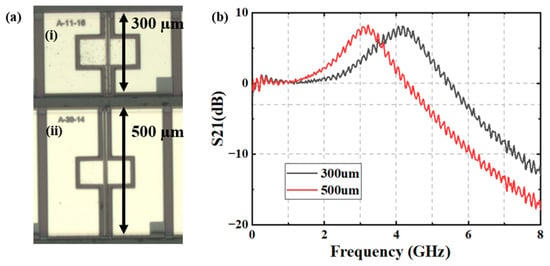
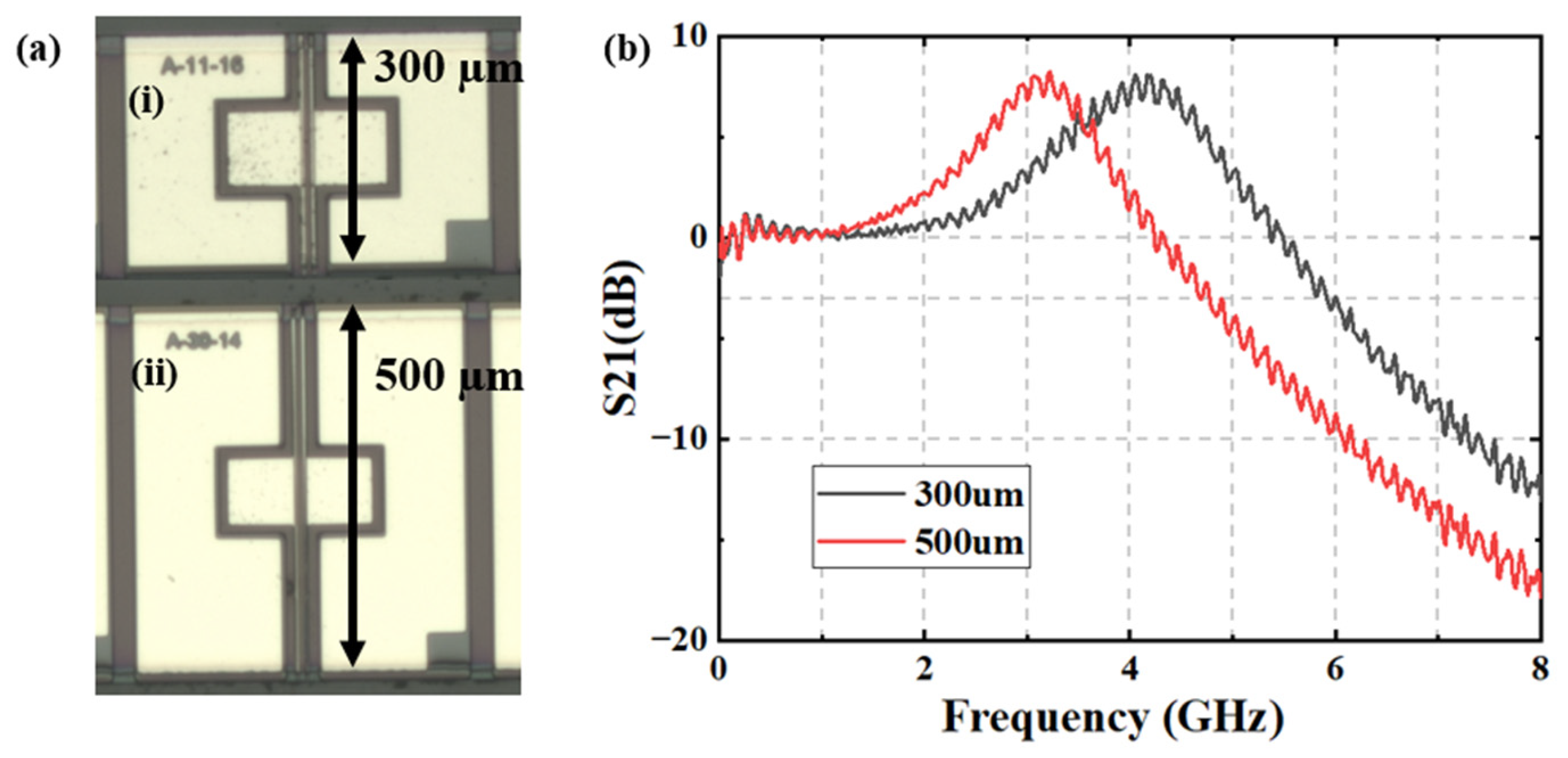
Figure 5a shows optical microscopic images of laser diodes with different cavity lengths. Except for the cavity length, these devices have the same ridge waveguide geometry and epitaxial layer structure, allowing for a direct comparison of the effect of cavity length on dynamic characteristics. The threshold currents of the DR-LD-300 and the DR-LD-500 are almost identical, both approximately 80 mA. To ensure consistent operating conditions, the injection current for both devices was fixed at approximately twice the threshold current.
Figure 5.
(a) Top-view optical microscope images of GaN-based laser diodes with cavity lengths. (i) 300 μm and (ii) 500 μm. (b) Small-signal modulation responses (S21) of the two laser diode samples were measured at an injection current of 160 mA.
As shown in Figure 5b, the two devices exhibit similar overall frequency responses. However, for the laser with the shorter cavity length, the modulation bandwidth is significantly enhanced. When the cavity length decreases from 500 μm to 300 μm, the measured −3 dB modulation bandwidth increases from 4.77 GHz to 5.92 GHz. Furthermore, the resonant peak of the short-cavity laser shifts to higher frequencies, indicating an increase in the relaxation resonance frequency. This improvement is mainly attributed to the reduction in the effective mode volume resulting from the shorter cavity length. A smaller mode volume results in a higher photon density at a given injection current, thereby enhancing the differential gain and increasing the relaxation resonance frequency. Therefore, the inherent modulation bandwidth of the laser diode is improved.
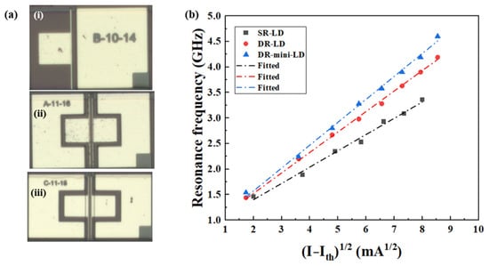
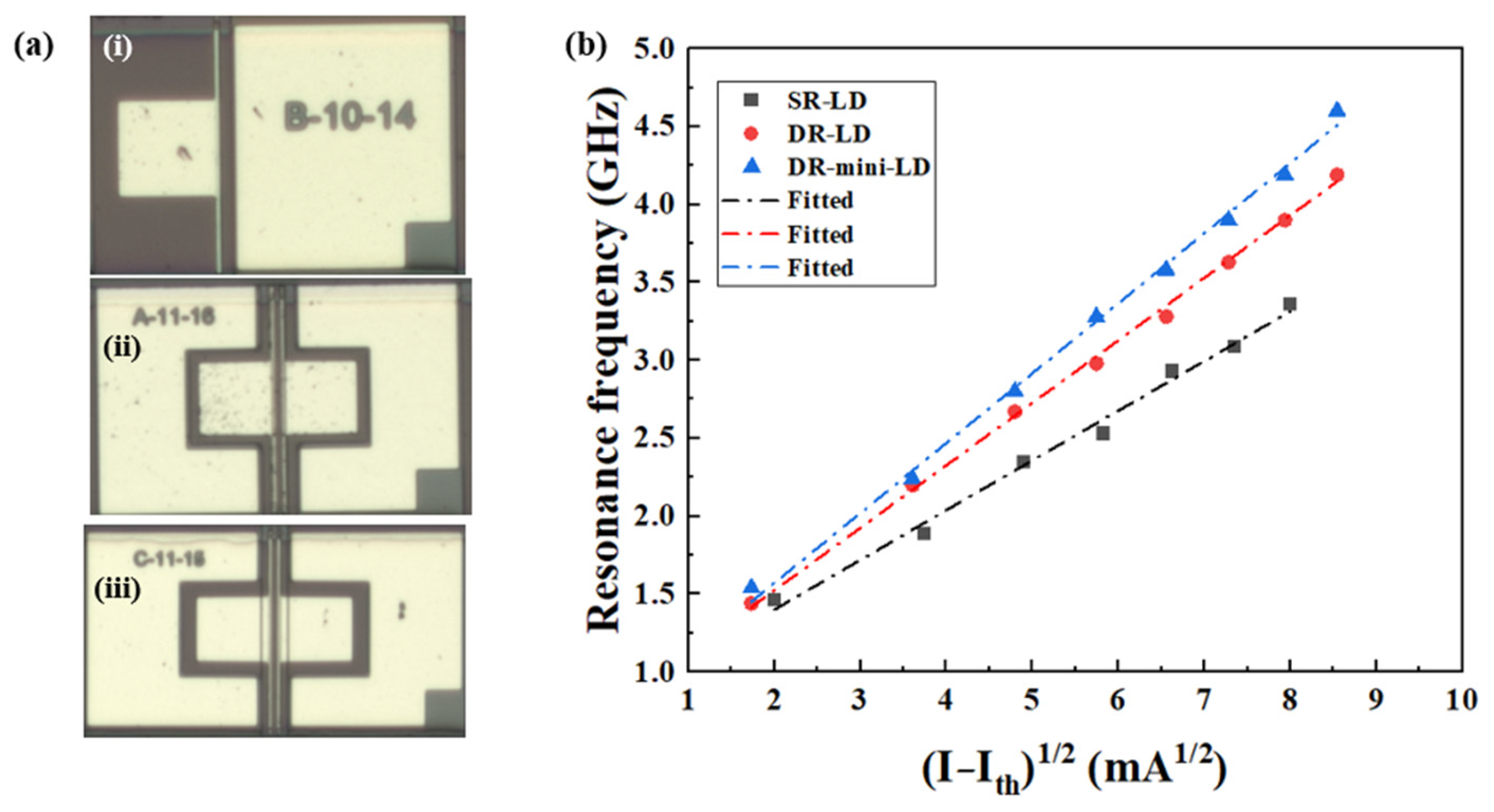
Figure 6a presents the optical microscope images of the three laser diode structures investigated in this study. From top to bottom, the devices are identified as (i) SR-LD, (ii) DR-LD, and (iii) DR-mini-LD, respectively.
Figure 6.
(a) Top-view optical microscope images of GaN-based laser diodes with different ridge/mesa configurations: from top to bottom, (i) SR-LD, (ii) DR-LD, and (iii) DR-mini-LD. (b) Relationship between resonant frequency and driving current for different structures. The solid symbols represent experimental data, and the dashed lines are linear fits.
Figure 6b presents the measured resonance frequency as a function of for the three laser structures. According to the carrier–photon rate equation model, the of a semiconductor laser can be expressed as proportional to the square root of the excess injection current above threshold:
This relationship arises from the coupling between carrier density and photon density in the active region. As the injection current increases above threshold, the carrier density increases, leading to enhanced stimulated emission and a higher differential gain. Consequently, the carrier–photon interaction becomes stronger, resulting in an increase in the relaxation resonance frequency.
Therefore, a linear dependence between and is expected, which is consistent with the experimental results shown in Figure 5b. The fitted slopes for the three structures are extracted to be 0.316 GHz/mA1/2, 0.403 GHz/mA1/2, and 0.449 GHz/mA1/2, respectively. The differences in slope reflect variations in the differential gain and effective mode volume among the devices.
We attribute this observation to the fact that the dual-ridge configuration enhances the differential gain and carrier–photon coupling strength. As a result, the relaxation resonance frequency increases more rapidly with current, yielding a larger modulation efficiency. The single-ridge structure exhibits a relatively large effective mode volume and weaker lateral confinement, limiting photon density and reducing the slope of the resonance frequency scaling. The dual-ridge structure with a large mesa represents an intermediate case, where enhanced confinement compared to the single-ridge laser improves the modulation response, but not as effectively as the small-mesa design.
Table 1 lists the test results for GaN-based LDs with different structures. These works demonstrate that optimizing the ridge and mesa geometry is an effective approach to increasing the relaxation resonance frequency and the intrinsic modulation bandwidth of GaN-based laser diodes, without altering the epitaxial structure. In particular, the DR-mini-LD shows clear advantages for high-speed modulation applications.
Table 1.
Summary of Key Experimental Results of GaN-based LDs.
4. Conclusions
In summary, our work shows that downscaling of cavity length and ridge structure engineering play crucial roles in enhancing the high-speed modulation performance of GaN-based laser diodes. Shortening the laser cavity reduces the effective optical mode volume, thereby increasing the relaxation resonance frequency and, consequently, improving the device’s intrinsic modulation bandwidth. By transitioning from a conventional single-ridge structure to a dual-ridge configuration, the dual-ridge laser with a smaller mesa size further enhances the device’s modulation bandwidth. These structural modifications have a positive impact on the frequency response. This work offers valuable guidance for the design and optimization of high-speed laser diodes. It paves the way for energy-efficient visible light communication systems and integrated photonics in the visible spectral region.
Author Contributions
Conceptualization, Z.W., J.H. and C.S.; methodology, Z.W., Z.Y.; software, Z.W. and J.H.; validation, Z.W.; formal analysis, Z.W.; investigation, Z.W.; resources, A.K., P.P., S.L., H.D., J.Z. (Jiangyong Zhang), J.Z. (Junwen Zhang) and C.S.; data curation, Z.W.; writing—original draft preparation, Z.W.; writing—review and editing, S.S.N., M.A. and C.S.; visualization, Z.W.; supervision, J.Z. (Junwen Zhang), N.C. and C.S.; funding acquisition, J.Z. (Junwen Zhang), N.C. and C.S. All authors have read and agreed to the published version of the manuscript.
Funding
This research is partially funded by the National Natural Science Foundation of China (62274042, 624B2045, 62525102); The Explorers Program of Shanghai (Basic Research Funding, 25TS1415500); AI for Science Program, Shanghai Municipal Commission of Economy and Informatization (2025-GZL-RGZN-BTBX-02036); Shanghai Rising-Star Program (24QB2705400).
Institutional Review Board Statement
Not applicable.
Informed Consent Statement
Not applicable.
Data Availability Statement
The data presented in this study are available on request from the first author.
Conflicts of Interest
Authors Shuiqing Li, Heqing Deng and Jiangyong Zhang were employed by the company Anhui GaN Semiconductor Co., Ltd. Author Chao Shen was employed by the company Shanghai Shenyu Tech Co., Ltd. The remaining authors declare that the research was conducted in the absence of any commercial or financial relationships that could be construed as a potential conflict of interest.
Abbreviations
The following abbreviations are used in this manuscript:
| VLC | visible light communication |
| LDs | laser diodes |
| LEDs | light-emitting diodes |
| UWOC | underwater wireless optical communication |
| GaN | gallium nitride |
| MOCVD | metal–organic chemical vapor deposition |
| RC | resistance–capacitance |
| QW | quantum well |
| EBL | electron blocking layer |
| EL | electroluminescence |
References
- Nakamura, S.; Mukai, T.; Senoh, M. Candela-class high-brightness InGaN/AlGaN double-heterostructure blue-light-emitting diodes. Appl. Phys. Lett. 1994, 64, 1687–1689. [Google Scholar] [CrossRef] [Scilit]
- Li, G.; Wang, W.; Yang, W.; Lin, Y.; Wang, H.; Lin, Z.; Zhou, S. GaN-based light-emitting diodes on various substrates: A critical review. Rep. Prog. Phys. 2016, 79, 056501. [Google Scholar] [CrossRef] [Scilit] [PubMed]
- Young, E.C.; Yonkee, B.P.; Wu, F.; Oh, S.H.; DenBaars, S.P.; Nakamura, S.; Speck, J.S. Hybrid tunnel junction contacts to III–nitride light-emitting diodes. Appl. Phys. Express 2016, 9, 022102. [Google Scholar] [CrossRef] [Scilit]
- Oh, S.H.; Yonkee, B.P.; Cantore, M.; Farrell, R.M.; Speck, J.S.; Nakamura, S.; DenBaars, S.P. Semipolar III–nitride light-emitting diodes with negligible efficiency droop up to ~1 W. Appl. Phys. Express 2016, 9, 102102. [Google Scholar] [CrossRef] [Scilit]
- Lee, C.; Shen, C.; Cozzan, C.; Farrell, R.M.; Speck, J.S.; Nakamura, S.; Ooi, B.S.; DenBaars, S.P. Gigabit-per-second white light-based visible light communication using near-ultraviolet laser diode and red-, green-, and blue-emitting phosphors. Opt. Express 2017, 25, 17480–17487. [Google Scholar] [CrossRef] [Scilit]
- Ali, M.F.; Jayakody, D.N.K.; Li, Y. Recent trends in underwater visible light communication (UVLC) systems. IEEE Access 2022, 10, 22169–22225. [Google Scholar] [CrossRef] [Scilit]
- McKendry, J.J.D.; Green, R.P.; Kelly, A.E.; Gong, Z.; Guilhabert, B.; Massoubre, D.; Gu, E.; Dawson, M.D. High-speed visible light communications using individual pixels in a micro light-emitting diode array. IEEE Photon. Technol. Lett. 2010, 22, 1346–1348. [Google Scholar] [CrossRef] [Scilit]
- Guo, Y.; Alkhazragi, O.; Kang, C.H.; Shen, C.; Mao, Y.; Sun, X.; Ng, T.K.; Ooi, B.S. A tutorial on laser-based lighting and visible light communications: Device and technology. Chin. Opt. Lett. 2019, 17, 040601. [Google Scholar] [CrossRef] [Scilit]
- Xu, H.; Ai, J.; Deng, T.; Ruan, Y.; Sun, D.; Liao, Y.; Cui, X.; Tian, P. Recent progress in GaN-based high-bandwidth micro-LEDs and photodetectors for high-speed visible light communication. Photonics 2025, 12, 730. [Google Scholar] [CrossRef] [Scilit]
- Oubei, H.M.; Duran, J.R.; Janjua, B.; Wang, H.-Y.; Tsai, C.-T.; Chi, Y.-C.; Ng, T.K.; Kuo, H.C.; He, J.H.; Alouini, M.-S. 4.8 Gbit/s 16-QAM-OFDM transmission based on compact 450-nm laser for underwater wireless optical communication. Opt. Express 2015, 23, 23302–23309. [Google Scholar] [CrossRef] [Scilit]
- Nakamura, S. First III–V-nitride-based violet laser diodes. J. Cryst. Growth 1997, 170, 11–15. [Google Scholar] [CrossRef] [Scilit]
- Nakamura, S. The roles of structural imperfections in InGaN-based blue light-emitting diodes and laser diodes. Science 1998, 281, 956–961. [Google Scholar] [CrossRef] [Scilit]
- Kang, J.-H.; Wenzel, H.; Freier, E.; Hoffmann, V.; Fricke, J.; Brox, O.; Matalla, M.; Einfeldt, S. Continuous-wave operation of 405 nm distributed Bragg reflector laser diodes based on GaN using 10th-order surface gratings. Photonics Res. 2022, 10, 1157–1161. [Google Scholar] [CrossRef] [Scilit]
- Hu, L.; Ren, X.; Liu, J.; Tian, A.; Jiang, L.; Huang, S.; Zhou, W.; Zhang, L.; Yang, H. High-power hybrid GaN-based green laser diodes with ITO cladding layer. Photonics Res. 2020, 8, 279–285. [Google Scholar] [CrossRef] [Scilit]
- Retamal, J.R.D.; Oubei, H.M.; Janjua, B.; Chi, Y.-C.; Wang, H.-Y.; Tsai, C.-T.; Ng, T.K.; Hsieh, D.-H.; Kuo, H.-C.; Alouini, M.-S.; et al. 4-Gbit/s visible light communication link based on 16-QAM OFDM transmission over remote phosphor-film converted white light by using blue laser diode. Opt. Express 2015, 23, 33656–33666. [Google Scholar] [CrossRef] [Scilit] [PubMed]
- Zafar, F.; Bakaul, M.; Parthiban, R. Laser-diode-based visible light communication: Toward gigabit class communication. IEEE Commun. Mag. 2017, 55, 144–151. [Google Scholar] [CrossRef] [Scilit]
- Yamaoka, S.; Diamantopoulos, N.-P.; Nishi, H.; Nakao, R.; Fujii, T.; Takeda, K.; Hiraki, T.; Tsurugaya, T.; Kanazawa, S.; Tanobe, H.; et al. Directly modulated membrane lasers with 108 GHz bandwidth on a high-thermal-conductivity silicon carbide substrate. Nat. Photon. 2021, 15, 28–35. [Google Scholar] [CrossRef] [Scilit]
- Dunn, A.; Poyser, C.; Dean, P.; Demić, A.; Valavanis, A.; Indjin, D.; Salih, M.; Kundu, I.; Li, L.; Akimov, A.; et al. High-speed modulation of a terahertz quantum cascade laser by coherent acoustic phonon pulses. Nat. Commun. 2020, 11, 835. [Google Scholar] [CrossRef] [Scilit]
- Watson, S.; Tan, M.; Najda, S.P.; Perlin, P.; Leszczynski, M.; Targowski, G.; Grzanka, S.; Kelly, A.E. Visible light communications using a directly modulated 422 nm GaN laser diode. Opt. Lett. 2013, 38, 3792–3794. [Google Scholar] [CrossRef] [Scilit]
- Chi, Y.-C.; Hsieh, D.-H.; Tsai, C.-T.; Chen, H.-Y.; Kuo, H.-C.; Lin, G.-R. 450-nm GaN laser diode enables high-speed visible light communication with 9-Gbps QAM-OFDM. Opt. Express 2015, 23, 13051–13059. [Google Scholar] [CrossRef] [Scilit]
- Lee, C.; Zhang, C.; Becerra, D.L.; Lee, S.; Forman, C.A.; Oh, S.H.; Farrell, R.M.; Speck, J.S.; Nakamura, S.; Bowers, J.E.; et al. Dynamic characteristics of 410 nm semipolar (2021) III-nitride laser diodes with a modulation bandwidth of over 5 GHz. Appl. Phys. Lett. 2016, 109, 10. [Google Scholar] [CrossRef] [Scilit]
- Najda, S.P.; Perlin, P.; Suski, T.; Marona, L.; Leszczyński, M.; Wisniewski, P.; Stanczyk, S.; Schiavon, D.; Slight, T.; Watson, M.A.; et al. GaN laser diode technology for visible-light communications. Electronics 2022, 11, 1430. [Google Scholar] [CrossRef] [Scilit]
- Mei, Y.; Weng, G.-E.; Zhang, B.-P.; Liu, J.-P.; Hofmann, W.; Ying, L.-Y.; Zhang, J.-Y.; Li, Z.-C.; Yang, H.; Kuo, H.-C. Quantum dot vertical-cavity surface-emitting lasers covering the ‘green gap’. Light Sci. Appl. 2017, 6, e16199. [Google Scholar] [CrossRef] [Scilit] [PubMed]
- Lau, K.; Gee, C.; Chen, T.; Bar-Chaim, N.; Ury, I. Signal-induced noise in fiber-optic links using directly modulated Fabry-Perot and distributed-feedback laser diodes. J. Lightwave Technol. 2002, 11, 1216–1225. [Google Scholar] [CrossRef] [Scilit]
- Wang, T. Topical Review: Development of overgrown semi-polar GaN for high efficiency green/yellow emission. Semicond. Sci. Technol. 2016, 31, 093003. [Google Scholar] [CrossRef] [Scilit]
- Gourley, P.L. Microstructured semiconductor lasers for high-speed information processing. Nature 1994, 371, 571–577. [Google Scholar] [CrossRef] [Scilit]
- Sun, L.; Wang, J.; Guan, C.; Fang, S.; Li, Z.; Hu, J.; Wang, Y.; Ooi, B.S.; Shi, J.; Li, Z.; et al. Down-scaling of GaN-based laser diodes for high-speed modulation characteristics. IEEE J. Sel. Top. Quantum Electron. 2024, 31, 1–8. [Google Scholar] [CrossRef] [Scilit]
- Wang, J.; Hu, J.; Guan, C.; Hou, Y.; Xu, Z.; Sun, L.; Wang, Y.; Zhou, Y.; Ooi, B.S.; Shi, J.; et al. High-speed GaN-based laser diode with modulation bandwidth exceeding 5 GHz for 20 Gbps visible light communication. Photonics Res. 2024, 12, 1186–1193. [Google Scholar] [CrossRef] [Scilit]
- Jia, H.; Hu, J.; Gu, Z.; Yang, Z.; Fan, D.; Zha, L.; Wu, J.; Guo, C.; Zhou, Y.; Shi, J.; et al. GaN-Based Laser Diode with a Trapezoidal EBL and an Unintentionally Doped Layer Reaching 7.8 GHz Modulation Bandwidth. ACS Photonics 2025, 12, 2120–2127. [Google Scholar] [CrossRef] [Scilit]
- Hu, J.; Gu, Z.; Jia, H.; Yang, Z.; Li, Z.; Wu, J.; Sun, L.; Sun, A.; Huang, O.; Xia, C.; et al. InGaN-based high-speed mini laser diode surpasses PAM-4 visible light links by over 30 Gbps. Sci. China Inf. Sci. 2026, 69, 132405. [Google Scholar] [CrossRef] [Scilit]

Disclaimer/Publisher’s Note: The statements, opinions and data contained in all publications are solely those of the individual author(s) and contributor(s) and not of MDPI and/or the editor(s). MDPI and/or the editor(s) disclaim responsibility for any injury to people or property resulting from any ideas, methods, instructions or products referred to in the content. |
© 2026 by the authors. Licensee MDPI, Basel, Switzerland. This article is an open access article distributed under the terms and conditions of the Creative Commons Attribution (CC BY) license.