


Abstract
The integration of micro-nano optical structures has become an essential strategy for overcoming the performance bottlenecks of quantum well infrared photodetectors (QWIPs), specifically by addressing the inherent inability of planar devices to couple with normally incident light due to intersubband transition selection rules. A critical factor in this integration is the precise spectral overlap between an optical mode and the material’s excitation mode. Therefore, achieving precise spectral engineering is indispensable. However, conventional electromagnetic simulations act as forward solvers, calculating optical responses based on given geometric parameters. They cannot directly perform inverse design, which involves deriving optimal geometric parameters directly from a desired optical response. Consequently, structural optimization is severely constrained by time-consuming trial-and-error iterations, which often struggle to find the global optimum in a complex design space. To overcome these limitations, this paper presents a comprehensive theoretical and numerical study proposing a deep learning framework for QWIPs coupled with all-dielectric micropillar structures. By establishing a structure-absorption spectrum dataset via finite difference time domain (FDTD) simulations, we developed a dual-network setup. For the forward prediction, a multilayer perceptron (MLP) maps geometric parameters (side length a and period p) to the absorption spectrum, achieving a computational speedup of seven orders of magnitude over traditional numerical simulations. Concurrently, a convolutional neural network (CNN) is employed for the inverse design, realizing on-demand design of geometric parameters based on target spectra with high reconstruction accuracy. Furthermore, the selected all-dielectric micropillar structures are highly compatible with mainstream semiconductor fabrication processes. This research provides an efficient, automated toolkit for the development of high-performance infrared photodetectors.
1. Introduction
Infrared detection technology plays an indispensable role in fields such as imaging [1], molecular sensing [2], and atmospheric monitoring [3,4]. Among various technologies, QWIPs occupy a prominent position in long-wave infrared (LWIR) detection due to their high uniformity in large-scale material growth, superior stability, and mature fabrication processes [5]. However, governed by intersubband transition selection rules, quantum wells can only absorb the electric field component perpendicular to the epitaxial layers (). This physical constraint prevents traditional planar devices from effectively coupling with normally incident light.
To overcome this limitation, researchers have introduced various micro-nano optical structures—including metallic antennas [6], photonic crystal slabs [7], and all-dielectric micropillars [8,9]—to modulate the incident light field. These structures generate a strong component, thereby enhancing light-matter interaction and improving the absorption efficiency of the quantum well layers. In designing such structures, the precise regulation of the spectral response (e.g., the synergistic optimization of resonant peak positions and absorption intensity) is of paramount importance.
Traditionally, geometric design heavily relies on electromagnetic modeling based on numerical simulations, such as the FDTDmethod [10]. Reaching a target response requires meticulous fine-tuning of geometric parameters through an iterative, trial-and-error process. However, the high computational costs and slow iteration speeds of these methods severely restrict design efficiency. Furthermore, FDTD lacks the inherent capability for inverse design, specifically in deriving geometric parameters from target spectral responses.
In recent years, deep learning (DL) has emerged as a powerful data-driven approach, offering new paradigms for photonic device design through its nonlinear mapping capabilities [11]. Once trained, DL models can map the relationship between device structures and their optical responses near-instantaneously, bypassing time-consuming numerical solvers. DL-based methods have already been successfully applied to broadband absorption enhancement [12], high-performance thermal emitters [13], and protein structure detection [14].
In this paper, we propose a deep learning-based forward-inverse prediction framework. For the forward model, inputting geometric parameters (side length a, period p) yields the QWIP absorption spectrum within 0.12 ms, representing a speedup of seven orders of magnitude over conventional electromagnetic simulations. For the inverse design model, providing a desired absorption spectrum allows for the direct retrieval of the corresponding geometric parameters. Physically, achieving this optimal absorption spectrum ensures the precise spectral overlap between the material’s excitation mode and the optical guided-mode resonance. This optical resonance provides the critical out-of-plane electric field () enhancement within the quantum well region, thereby maximizing the light-matter interaction. This work provides an efficient, automated toolkit for the realization of high-performance infrared detectors.
2. Materials and Methods
2.1. Device Structure and Design
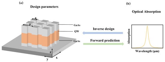
As illustrated in Figure 1a, the proposed device consists of an array of square all-dielectric micropillars. The height of the micropillars is fixed at 3.9 μm, while the side length (a) and the period (p) are varied to modulate the optical response. The device architecture comprises a three-layer vertical stack: a 1.8 μm thick top GaAs layer, a 1.5 μm thick central GaAs/AlGaAs multi-quantum well (QW) active layer, and a 0.6 μm thick bottom GaAs layer. The substrate is GaAs.
Figure 1.
Schematic of the deep learning-based QWIP structure and its forward and inverse design workflows. (a) Design model of the all-dielectric micropillar array detector, defining the materials of each layer and geometric parameters (side length a, period p); (b) absorption spectra of the quantum well micropillar array.
To facilitate photocurrent extraction, 300 nm wide conductive bridges are integrated between the square micropillars. This configuration enables the incident light field to be effectively confined within the micropillar cavities. Furthermore, the design is highly compatible with semiconductor fabrication processes.
2.2. FDTD Numerical Simulation
To establish a comprehensive “structure-to-spectrum” dataset for deep learning, we performed large-scale batch simulations using the FDTDmethod. The simulation model primarily incorporates two material types: bulk GaAs and the GaAs/AlGaAs QW. The QW layer, formed by periodic repetitions of GaAs and AlGaAs, is modeled as an anisotropic medium, .Its dielectric functions in the x and y directions are approximately equivalent to those of GaAs, . The dielectric function in the z direction () follows a Lorentzian lineshape [15,16,17]:
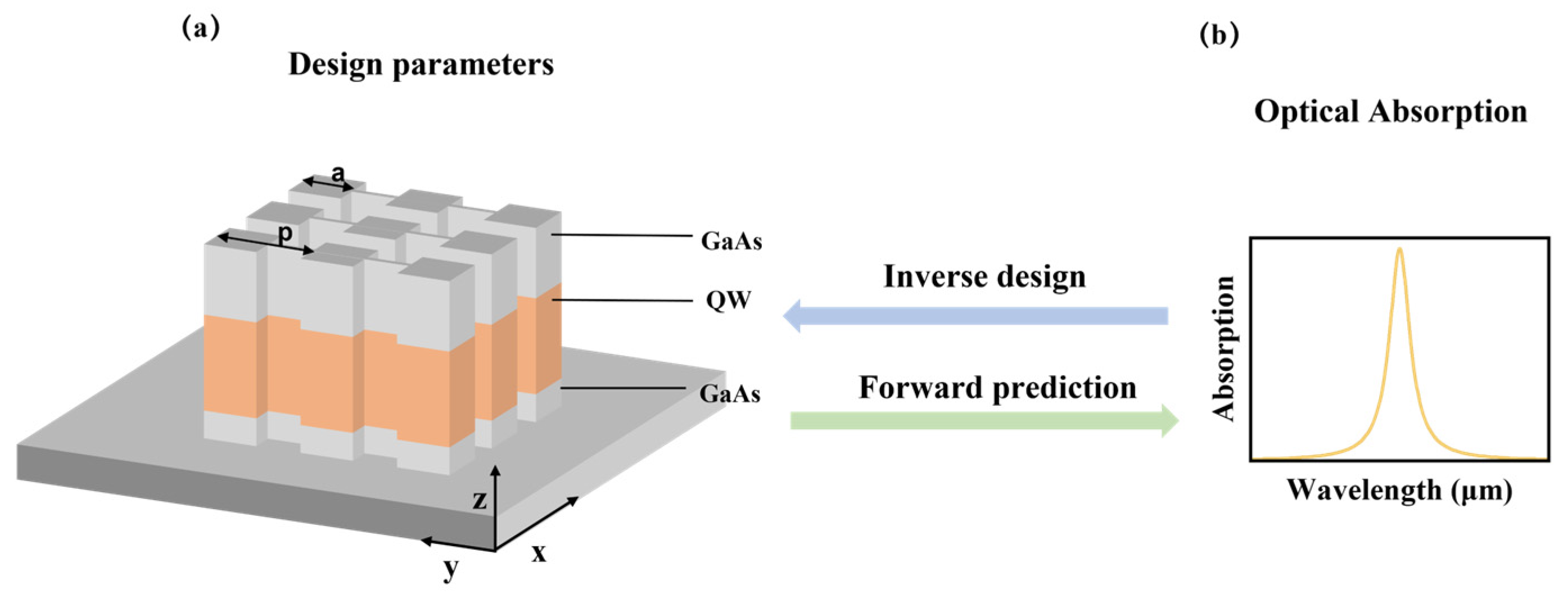
and represent the peak response frequency and the damping constant of the QW, respectively. These parameters are obtained by fitting the photocurrent spectrum of a 45° mesa device with a Lorentzian lineshape. denotes the imaginary part of the dielectric constant associated with the intersubband absorption at the peak response frequency. The real and imaginary parts of the are illustrated in Figure 2a. Notably, the imaginary part features a peak at a wavelength of 10.2 μm, dictating the material’s intersubband excitation. Numerical simulations were conducted using Lumerical FDTD Solutions 2023.
Figure 2.
Material dielectric properties and dataset distribution. (a) Real and imaginary parts of the z-direction complex dielectric function () dispersion for the GaAs/AlGaAs QW layer. (b) Dataset of 400 absorption spectra generated through FDTD simulations with varying geometric parameters (side length a and period p). (c) Absorption spectra for a fixed micropillar side length a = 2.1 μm while varying the period p from 3.4 μm to 5.0 μm. (d) Absorption spectra for a fixed period p = 4.8 μm while varying the side length a from 1.6 μm to 2.0 μm.
To accurately model the periodicity of the device, periodic boundary conditions were applied along the x and y axes, while perfectly matched layer (PML) conditions were employed along the z axis. The simulation mesh was set to a uniform resolution of 0.1 μm; this mesh fineness is sufficiently rigorous for the micron-scale dimensions of the unit cell, ensuring both computational convergence and high numerical accuracy. The excitation source was defined as a z-axis-oriented plane wave with normal incidence upon the micropillar-coupled QWIP array. Furthermore, frequency-domain field profile monitors were positioned directly above and below the device to capture the reflectance () and transmittance () spectra.
2.3. Dataset Construction
The absorption spectrum (A) of the micropillar-coupled QWIP array was calculated using the relation . To construct a dataset for the deep learning models, we systematically swept the geometric parameters of the micropillars. As illustrated in Figure 2b, the side length (a) was varied from 1.5 μm to 3.9 μm, while the period (p) was varied from 2.0 μm to 10.6 μm. This extensive parameter space ensures that the generated dataset, comprising 400 distinct absorption spectra, can cover a significantly broader resonance wavelength band. Furthermore, the spectral behavior exhibits a strong dependence on these geometric variations. For instance, as shown in Figure 2c, when the side length is fixed, increasing the period p leads to a redshift in the resonance peak. A similar redshift phenomenon is observed in Figure 2d when the period is fixed and the side length a is increased. Therefore, by simultaneously varying both the side length and the period over a wide range, we successfully mapped a highly comprehensive and continuous optical response space. Finally, for the training of the deep learning models, 80% of the generated data (320 samples) was used for the training set, while the remaining 20% (80 samples) served as the testing set to evaluate the models’ generalization capability.
3. Results and Discussion
3.1. Forward Prediction Model Based on MLP
Leveraging the established structure-to-spectrum dataset, we first focused on the forward prediction of absorption spectra. The forward prediction model employs a MLP architecture. Despite its structural simplicity, the MLP is capable of approximating any continuous function and has been extensively utilized in nanophotonics research [18,19,20].
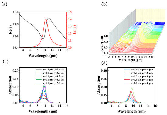
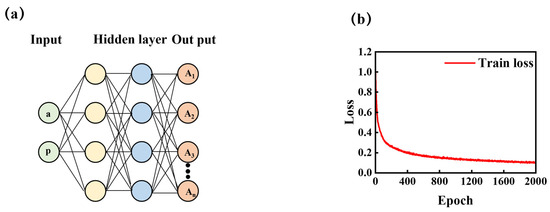
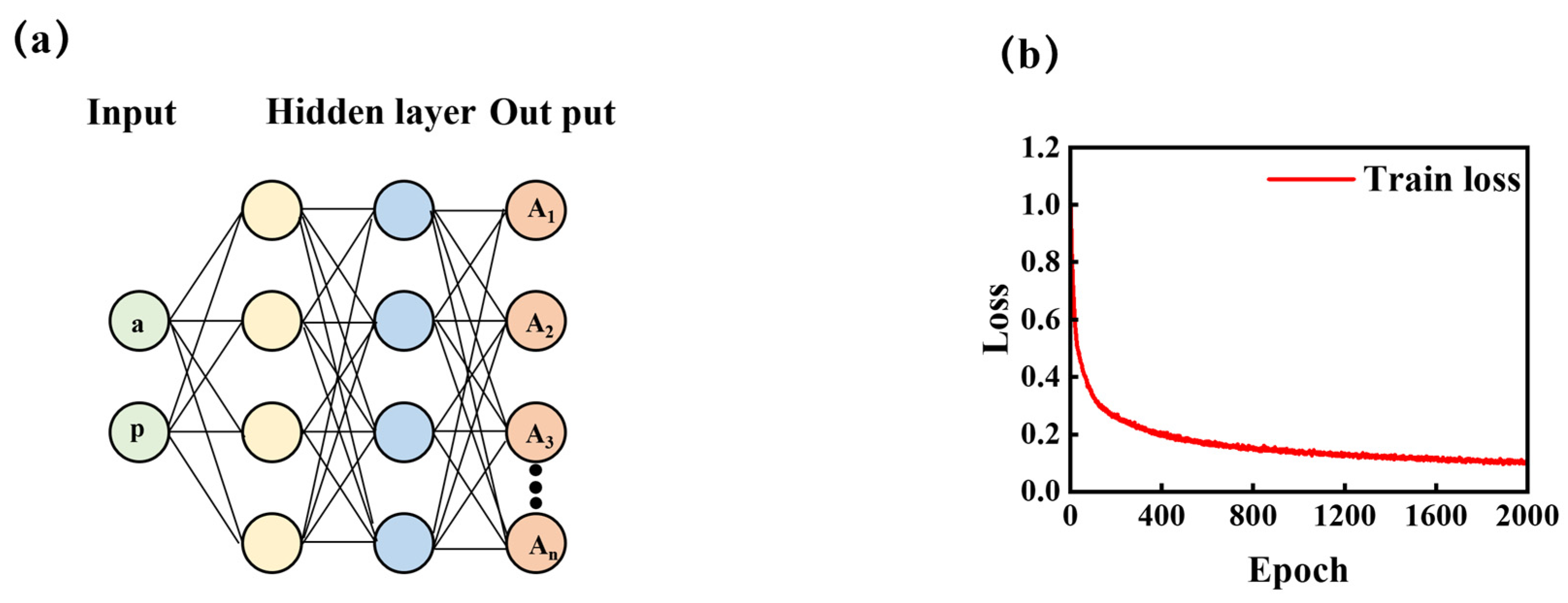
As depicted in Figure 3a, the input layer receives normalized geometric parameters, specifically the side length (a) and period (p) of the micropillars. The hidden layers are designed with 200, 300, 400, and 500 neurons, respectively. To enhance the model’s generalization capability and mitigate the risk of overfitting, a Dropout strategy with a rate of 0.2 is implemented. Rectified Linear Unit (ReLU) functions are employed as the activation mechanism for all hidden layers to handle non-linear mapping, while the final output layer generates a 500-dimensional vector representing the predicted absorption spectrum.
Figure 3.
MLP model and training. (a) Schematic of the MLP network architecture; (b) Convergence curve of the MSE loss function during training.
The training process of the forward network is optimized using the mean squared error (MSE) loss function, defined as:
where and denote the ground-truth and predicted absorption values, respectively. The model was implemented and trained using the PyTorch framework. To ensure stable convergence, both the input geometric features and the output spectral data were standardized using the StandardScaler method. We utilized the Adam optimizer with a learning rate of 0.0002 to minimize the MSE loss function. Training was performed using mini-batch stochastic gradient descent with a batch size of 64. The model was trained for 2000 epochs on an NVIDIA (NVIDIA Corp., Santa Clara, CA, USA) GeForce RTX 4060 GPU to ensure complete convergence of the training loss. As illustrated in Figure 3b, the training loss converges rapidly, indicating that the model has effectively captured the underlying physical mapping between the geometric structures and their optical responses.
3.2. Infrared Absorption Spectrum Prediction
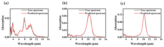
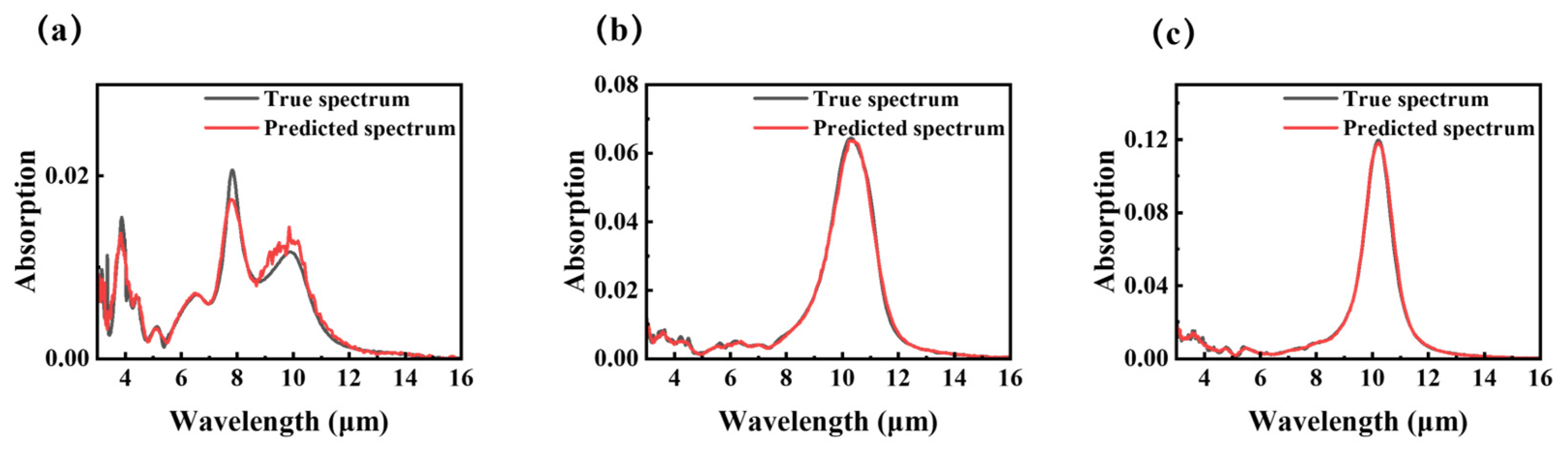
To evaluate the predictive performance of the forward prediction model, three representative samples were selected from the testing set. Specifically, Figure 4a demonstrates that the MLP model can accurately reconstruct complex multi-peak spectral features. Meanwhile, Figure 4b,c illustrate its capability to reliably predict single-peak spectra with higher absorption rates. Across these varied optical responses, the predicted resonance peak positions and the full width at half maximum (FWHM) are highly consistent with the ground truth.
Figure 4.
Comparison between predicted spectra (red solid lines) and FDTD-simulated spectra (black solid lines) for three typical structures in the test set. (a–c) The geometric parameters for these cases are: a = 1.6 μm p = 3.8 μm, a = 2.4 μm p = 5.6 μm, a = 2.6 μm p = 4.0 μm, respectively.
Furthermore, the deep learning framework offers a substantial advantage in computational efficiency. Evaluated on an NVIDIA GeForce RTX 4060 GPU, the average inference time of the trained MLP model is approximately 0.12 ms per spectrum. In comparison, a conventional FDTD numerical simulation for a single spectrum typically requires about 20 min. This indicates that the proposed deep learning approach achieves a computational speedup of seven orders of magnitude (107), which can significantly accelerate the spectrum prediction process.
3.3. Inverse Design Model Based on CNN
To rapidly retrieve the geometric parameters corresponding to a desired spectrum, we implemented an inverse design framework. For the inverse design model, we employed a CNN. CNN is a deep learning architecture that efficiently extracts data features using convolutional layers. It is particularly well-suited for processing spectral data, as it can effectively capture local correlations within the spectra [21,22].
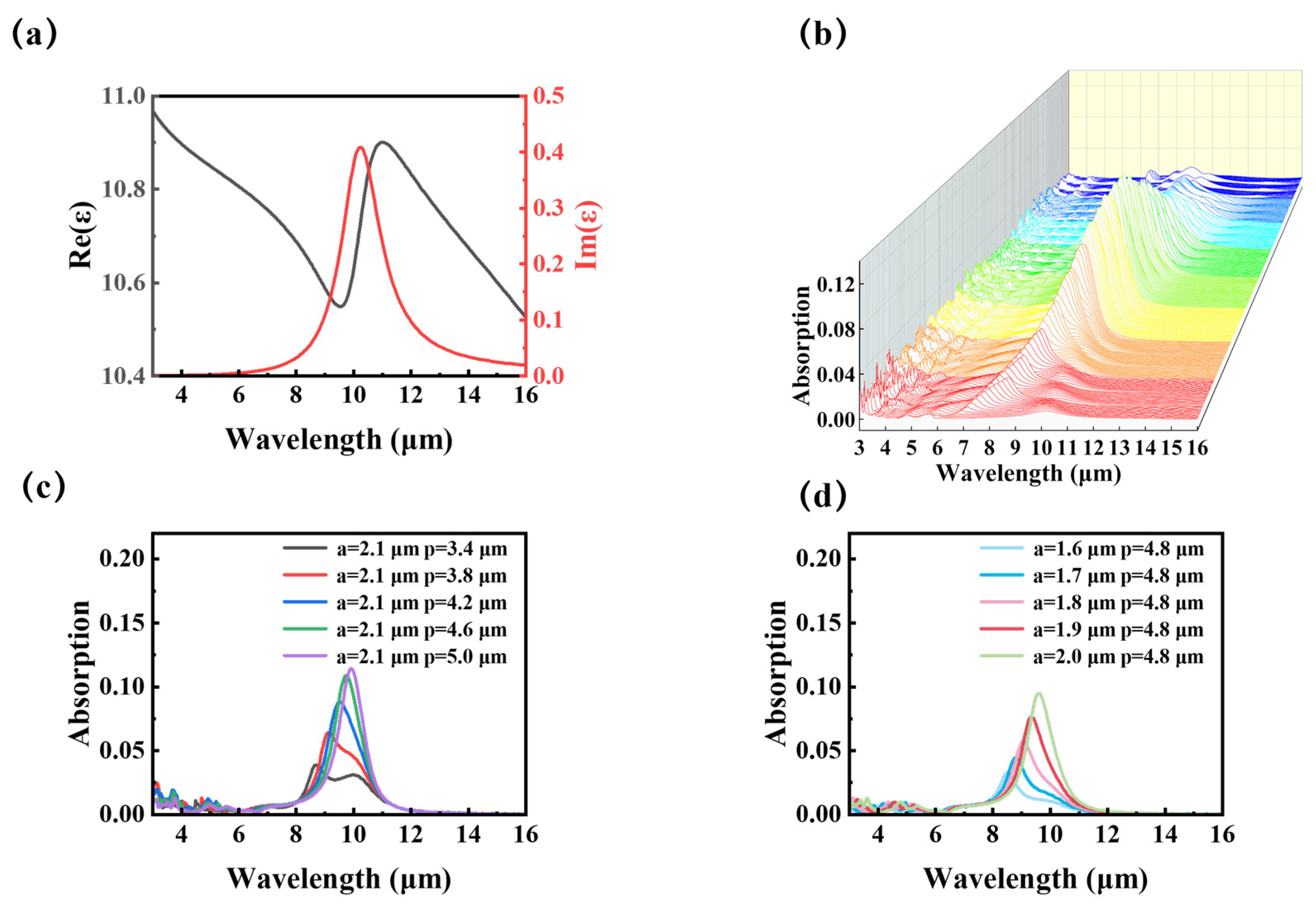
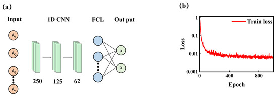
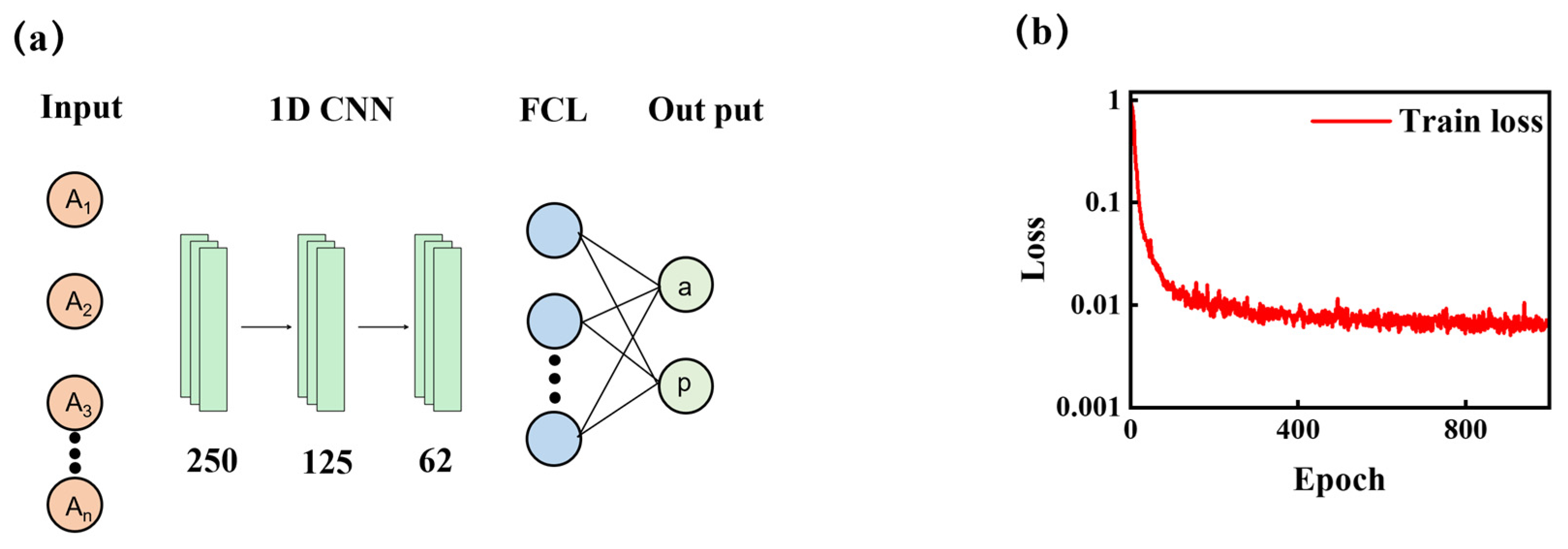
As illustrated in Figure 5a, the CNN backbone consists of three sequential 1D convolutional blocks. Each block performs a 1D convolution operation followed by a pooling layer, which progressively downsamples the sequence length of the spectral features. Specifically, the input spectrum vector of length 500 is first processed and compressed to a feature length of 250 after the first convolutional block. The subsequent two blocks continuously extract higher-level abstract features, further reducing the feature dimensions to 125 and 62, respectively. Following this hierarchical feature extraction process, the final 1D feature maps (length 62) are flattened and fed into a fully connected (FC) network. The network ultimately converges to a 2-node output layer, accurately yielding the targeted geometric parameters a and p.
Figure 5.
CNN model and training. (a) Architecture of the inverse design model based on a CNN; (b) Training loss function curve for the inverse network.
During model training, we adopted MSE as the loss function, defined as:
where and represent the ground-truth and predicted geometric parameters, respectively. The network was optimized using the Adam optimizer with an initial learning rate of 0.0001. To ensure robust feature learning and stable gradient updates, the model was trained with a batch size of 32 for 1000 epochs.
As shown in Figure 5b, the loss function converges rapidly during training and remains stable, indicating that the model has accurately captured the physical mapping from the spectral response back to the geometric structure.
3.4. Geometric Design and Physical Mechanism of the Devices
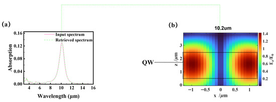
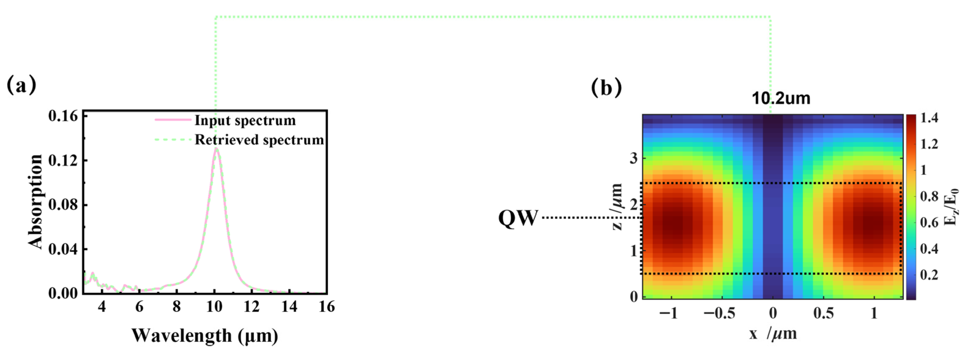
To verify the accuracy of the inversely designed parameters, we fed a preset target absorption spectrum into the network and imported the model’s output geometric parameters into the FDTD simulation environment for secondary validation. As depicted in Figure 6a, the inversely reconstructed spectrum highly coincides with the input target spectrum, demonstrating the model’s exceptional precision in navigating the geometric parameter space.
Figure 6.
Performance of the inverse design model and validation of physical mechanisms. (a) Comparison between the target spectrum (pink solid line) and the simulated spectrum (green dashed line) reconstructed using parameters predicted by the inverse model; (b) Localized electric field distribution () within the micropillar at the resonance wavelength of 10.2 μm. Where denotes the incident field amplitude.
From a physical perspective, the remarkable absorption enhancement stems from the synergy of two critical mechanisms. First, as shown in Figure 6b, the micropillar array excites a guided-mode resonance (GMR) that diffractively converts normally incident light into a strong out-of-plane electric field (), providing near-field enhancement. Second, at the resonant wavelength of 10.2 μm, this optical mode precisely overlaps with the material’s excitation mode (dictated by the imaginary part of the quantum wells’ dielectric function). The simultaneous spatial enhancement and exact spectral matching significantly enhance light-matter coupling, directly yielding the high absorption spectrum. This underlying mechanism fully validates the physical reliability of our deep learning design.
4. Conclusions
In this paper, we proposed a deep learning-driven approach to optimize the performance of all-dielectric micropillar QWIPs. Based on FDTD simulations, a comprehensive dataset comprising 500 structure-spectrum samples was constructed. For forward spectrum prediction, our developed MLP model achieves high-precision forward absorption spectrum prediction with a computational speedup of seven orders of magnitude over FDTD. For inverse geometric design, the CNN model directly predicts geometric parameters from a desired target spectrum, achieving on-demand inverse design, which is a capability inherently absent in conventional electromagnetic simulation software. Furthermore, near-field analysis reveals that GMR strongly enhances the internal electric field, and the high absorption is ultimately realized through the precise spectral matching between this optical mode and the QW material’s excitation mode. Therefore, the proposed method provides a rapid and precise DL framework for QWIP design. Future work will focus on the experimental fabrication of the optimal devices generated by this deep learning-assisted design, while exploring the extension of this methodology to the intelligent design of other complex optoelectronic devices.
Author Contributions
Conceptualization, W.L., T.L. and P.X.; methodology, P.X. and R.X.; software, P.X. and R.X.; validation, P.X.; formal analysis, P.X.; investigation, P.X.; resources, W.L. and T.L.; data curation, P.X. and R.X.; writing—original draft preparation, P.X.; writing—review and editing, W.L., T.L. and R.X.; visualization, P.X.; supervision, W.L. and T.L.; project administration, W.L. and T.L.; funding acquisition, W.L. and T.L. All authors have read and agreed to the published version of the manuscript.
Funding
This work was financially supported by National Natural Science Foundation of China (Grant Nos. U2241219, T.L.), Chinese Academy of Sciences (Grant Nos. XDB0580000, W.L.; GJ0090406, T.L.), National Natural Science Foundation of China (Grant Nos. 12393833, T.L.; 12227901, W.L.; 12174416, L.Y.; 11991063, T.L.), and the Science and Technology Commission of Shanghai Municipality (Grant No. 23JC1404100, B.Y.).
Data Availability Statement
The original contributions presented in this study are included in the article. Further inquiries can be directed to the corresponding authors.
Conflicts of Interest
The authors declare no conflicts of interest.
References
- Mu, G.; Tan, Y.; Bi, C.; Liu, Y.; Hao, Q.; Tang, X. Visible to Mid-Wave Infrared PbS/HgTe Colloidal Quantum Dot Imagers. Nat. Photonics 2024, 18, 1147–1154. [Google Scholar] [CrossRef] [Scilit]
- Rosas, S.; Biswas, S.K.; Adi, W.; Kuruoglu, F.; Beisenova, A.; Patankar, M.S.; Yesilkoy, F. Mass-Manufactured Gradient Plasmonic Metasurfaces for Enhanced Mid-IR Spectrochemical Analysis of Complex Biofluids. Adv. Mater. 2025, 37, e04355. [Google Scholar] [CrossRef] [Scilit]
- Shen, F.; Chen, D.; Wang, G.; Lu, J.; Hu, X.; Gao, X.; Fertein, E.; Chen, W. Real-Time Monitoring of CH4 and N2O Emissions from Livestock Using Mid-Infrared External Cavity Quantum Cascade Laser Absorption Spectroscopy. J. Quant. Spectrosc. Radiat. Transf. 2024, 327, 109131. [Google Scholar] [CrossRef] [Scilit]
- Reconstruction of Patagonia’s Glacial History Informs Key Global Climate Drivers. Nat. Geosci. 2024, 17, 381–382. [CrossRef] [Scilit]
- Xiao, Y.; Zhu, H.; Deng, K.; Wang, P.; Li, Q.; He, T.; Zhang, T.; Miao, J.; Li, N.; Lu, W.; et al. Progress and Challenges in Blocked Impurity Band Infrared Detectors for Space-Based Astronomy. Sci. China Phys. Mech. Astron. 2022, 65, 287301. [Google Scholar] [CrossRef] [Scilit]
- Nga Chen, Y.; Todorov, Y.; Askenazi, B.; Vasanelli, A.; Biasiol, G.; Colombelli, R.; Sirtori, C. Antenna-Coupled Microcavities for Enhanced Infrared Photo-Detection. Appl. Phys. Lett. 2014, 104, 031113. [Google Scholar] [CrossRef] [Scilit]
- Wu, W.; Bonakdar, A.; Mohseni, H. Plasmonic Enhanced Quantum Well Infrared Photodetector with High Detectivity. Appl. Phys. Lett. 2010, 96, 161107. [Google Scholar] [CrossRef] [Scilit]
- Liu, W.; Jiang, X.; Xia, H.; Deng, W.; Xin, R.; Yu, L.; Li, N.; Lu, W.; Li, T. Multiplied Absorption in Subwavelength Self-Grating-Coupled Multi-Layer Quantum Wells with Reduced Dark Current. Infrared Phys. Technol. 2024, 136, 104986. [Google Scholar] [CrossRef] [Scilit]
- Xin-Yang, J.; Wei-Wei, L.; Tian-Xin, L.; Hui, X.; Wei-Jie, D.; Li, Y.; Yu-Ying, L.; Wei, L. Enhanced Absorption of Infrared Light for Quantum Wells in Coupled Pillar-Cavity Arrays. Opt. Express 2023, 31, 7090. [Google Scholar] [CrossRef] [Scilit]
- Teixeira, F.L.; Sarris, C.; Zhang, Y.; Na, D.-Y.; Berenger, J.-P.; Su, Y.; Okoniewski, M.; Chew, W.C.; Backman, V.; Simpson, J.J. Finite-Difference Time-Domain Methods. Nat. Rev. Methods Primer 2023, 3, 75. [Google Scholar] [CrossRef] [Scilit]
- Ma, W.; Liu, Z.; Kudyshev, Z.A.; Boltasseva, A.; Cai, W.; Liu, Y. Deep Learning for the Design of Photonic Structures. Nat. Photonics 2021, 15, 77–90. [Google Scholar] [CrossRef] [Scilit]
- Ahmed, W.W.; Cao, H.; Xu, C.; Farhat, M.; Amin, M.; Li, X.; Zhang, X.; Wu, Y. Machine Learning Assisted Plasmonic Metascreen for Enhanced Broadband Absorption in Ultra-Thin Silicon Films. Light Sci. Appl. 2025, 14, 42. [Google Scholar] [CrossRef] [Scilit]
- Xiao, C.; Liu, M.; Yao, K.; Zhang, Y.; Zhang, M.; Yan, M.; Sun, Y.; Liu, X.; Cui, X.; Fan, T.; et al. Ultrabroadband and Band-Selective Thermal Meta-Emitters by Machine Learning. Nature 2025, 643, 80–88. [Google Scholar] [CrossRef] [Scilit]
- Wu, C.; Yang, S.; Zeng, K.; Dai, X.; Duan, Y.; Zhang, S.; Ma, P.; Guo, X.; Zhang, S.; Yang, X.; et al. Physics-Informed Deep Learning for Plasmonic Sensing of Nanoscale Protein Dynamics in Solution. Sci. Adv. 2025, 11, eadw0783. [Google Scholar] [CrossRef] [Scilit] [PubMed]
- Tang, W.; Zhou, J.; Zheng, Y.; Zhou, Y.; Hao, J.; Chen, X.; Lu, W. All-Dielectric Resonant Waveguide Based Quantum Well Infrared Photodetectors for Hyperspectral Detection. Opt. Commun. 2018, 427, 196–201. [Google Scholar] [CrossRef] [Scilit]
- Zhao, F.; Zhang, C.; Chang, H.; Hu, X. Design of Plasmonic Perfect Absorbers for Quantum-Well Infrared Photodetection. Plasmonics 2014, 9, 1397–1400. [Google Scholar] [CrossRef] [Scilit]
- Dini, D.; Köhler, R.; Tredicucci, A.; Biasiol, G.; Sorba, L. Microcavity Polariton Splitting of Intersubband Transitions. Phys. Rev. Lett. 2003, 90, 116401. [Google Scholar] [CrossRef] [Scilit]
- Malkiel, I.; Mrejen, M.; Nagler, A.; Arieli, U.; Wolf, L.; Suchowski, H. Plasmonic Nanostructure Design and Characterization via Deep Learning. Light Sci. Appl. 2018, 7, 607. [Google Scholar] [CrossRef] [Scilit] [PubMed]
- Ma, W.; Cheng, F.; Liu, Y. Deep-Learning-Enabled On-Demand Design of Chiral Metamaterials. ACS Nano 2018, 12, 6326–6334. [Google Scholar] [CrossRef] [Scilit] [PubMed]
- Liu, D.; Tan, Y.; Khoram, E.; Yu, Z. Training Deep Neural Networks for the Inverse Design of Nanophotonic Structures. ACS Photonics 2018, 5, 1365–1369. [Google Scholar] [CrossRef] [Scilit]
- Ho, C.-S.; Jean, N.; Hogan, C.A.; Blackmon, L.; Jeffrey, S.S.; Holodniy, M.; Banaei, N.; Saleh, A.A.E.; Ermon, S.; Dionne, J. Rapid Identification of Pathogenic Bacteria Using Raman Spectroscopy and Deep Learning. Nat. Commun. 2019, 10, 4927. [Google Scholar] [CrossRef] [Scilit] [PubMed]
- Huang, L.; Sun, H.; Sun, L.; Shi, K.; Chen, Y.; Ren, X.; Ge, Y.; Jiang, D.; Liu, X.; Knoll, W.; et al. Rapid, Label-Free Histopathological Diagnosis of Liver Cancer Based on Raman Spectroscopy and Deep Learning. Nat. Commun. 2023, 14, 48. [Google Scholar] [CrossRef] [Scilit] [PubMed]
Disclaimer/Publisher’s Note: The statements, opinions and data contained in all publications are solely those of the individual author(s) and contributor(s) and not of MDPI and/or the editor(s). MDPI and/or the editor(s) disclaim responsibility for any injury to people or property resulting from any ideas, methods, instructions or products referred to in the content. |
© 2026 by the authors. Licensee MDPI, Basel, Switzerland. This article is an open access article distributed under the terms and conditions of the Creative Commons Attribution (CC BY) license.