


Abstract
The avalanche photodiode (APD) is an optoelectronic detector with superior sensitivity that typically requires a high operating voltage. Reducing the avalanche region size could lower the breakdown voltage, but at the cost of increased excess noise. In this work, a scattering-engineered APD (SE APD) is proposed to reduce the operating voltage while maintaining a low excess noise merit. In SE APD, a special staggered-finger doping profile is used to spatially separate the electron-ionization path and the hole-transport path via scattering mechanisms, thereby enabling electron unipolar ionization. In SE APD, avalanche occurs at a very low reverse bias of ~2 V in the current–gain–voltage test; an extremely low ionization coefficient ratio (k-value) of 0.003 @ gain = 40 is verified by the noise power spectral density test. A low temperature-dependent breakdown drift coefficient of ~10 mV/K is obtained, indicating good thermal stability. Through comparative experiments, it is demonstrated that the SE APD can increase the gain–bandwidth product by fivefold when compared with the traditional APD structure. Furthermore, the width of the electron ionization multiplication path should be moderate, allowing holes to scatter into the transport path while retaining more electrons within the multiplication path.
1. Introduction
Due to its internal gain, the avalanche photodiode (APD) offers superior sensitivity compared with a traditional photodiode (PD) [1,2]. This internal gain originates from impact ionization, where multiplied electron–hole pairs are generated [3]. Liu et al. have shown that simply transforming a PD into an APD by raising the bias voltage can significantly improve receiver sensitivity [4]. Therefore, APD is an important optoelectronic device and can be widely used in long-haul optical communication, optical interconnection, electronic–photonic integrated circuits, lidar, and so on [5,6,7,8,9,10].
According to the local field theory established by McIntyre [11], the impact ionization coefficient ratio k-value is important for APD since it decides the excess noise factor:
The excess noise power could thus be described as
In Equations (1) and (2) M is the avalanche gain, q is the charge quantity, I is the total current participating in the avalanche process, and B is the bandwidth. Excess noise power can degrade the signal-to-noise ratio and, in turn, affect the sensitivity performance, which is the key merit of APDs. A lower k-value can also benefit the gain–bandwidth product (GBP) of the APD device [12]. Ge-on-Si (Ge/Si) APD combines the advantages of low k-value in bulk Si (k = 0.02) and Ge absorption at 1550 nm. Ge/Si APD is also compatible with the CMOS platform, which is convenient for mass production [13]. Therefore, Ge/Si APD is a promising candidate for PIC applications that usually require large-scale integration and low power consumption. The operating voltage of Ge/Si APD is commonly lower than that of III–V APD counterparts but is still higher than ~10 V [6,10,14], which brings challenges to the design of the driving circuits and the power consumption.
There have been attempts to reduce the operating voltage of an APD by reducing the avalanche-region size and carefully designing the electric-field profile. However, shortening the avalanche region could increase the electric field to achieve prominent avalanche gain, which could introduce bipolar ionization, raising k-value and the excess noise. In a report about Si APD with only a 50 nm avalanche region and a −8 V operating voltage, the k-value is confirmed to be 0.28, which is much higher than that of the bulk Si of ~0.02 [15]. In another report regarding Ge/Si APD, a −7.2 V breakdown voltage and 8 × 260 Gb/s signal reception have been realized, and a k-value of 0.06 was obtained by utilizing a gradient electric field and an avalanche region of ~200 nm [16]. A similar cascaded electric-field method has also been reported for III–V APDs [17,18]. Therefore, new mechanisms and avalanche-region designs are urgently needed to achieve low-noise performance in low-operating-voltage APDs with short avalanche regions.
In this work, a scattering-engineered APD (SE APD) is proposed to suppress excess noise in low-operating-voltage APDs. In carefully designed Si avalanche structures with tailored doping profiles, the electron ionization path and the hole transport path can be separated by scattering mechanisms and so electron unipolar ionization can be realized. To verify the theory, Ge/Si waveguide APDs with four different avalanche structures are designed and fabricated using the standard CMOS process at United Microelectronics Center Co., Ltd. (CUMEC). The avalanche properties are investigated and verified via a current–gain–voltage (I–G–V) test, and it is found that a prominent gain can appear at a mere ~2 V reverse bias. The excess noise experiments are carried out by a noise power spectral density (NPSD) test system schematically depicted in Figure S1 (Supplementary Material), and the k-value of each SE APD is analyzed. An extremely low k-value of 0.003 is obtained in the best-optimized SE APD. The electric field at representative gain points for each APD is analyzed, and it is found that the best-optimized SE APD requires the lowest electric field to achieve a given gain. By optimizing the SE APD structure, the GBP is improved by five times when compared with APD with bipolar ionization. Additionally, a low breakdown-voltage temperature-drift coefficient of ~10 mV/K is obtained in the SE APD by a temperature-dependent G–V test, indicating good temperature stability. Low-voltage and low-noise performance is achieved simultaneously in the proposed SE APD. This work could provide significant insights into the future design of low-operating-voltage, low-noise, high-GBP APDs.
2. Materials and Methods
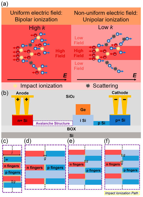
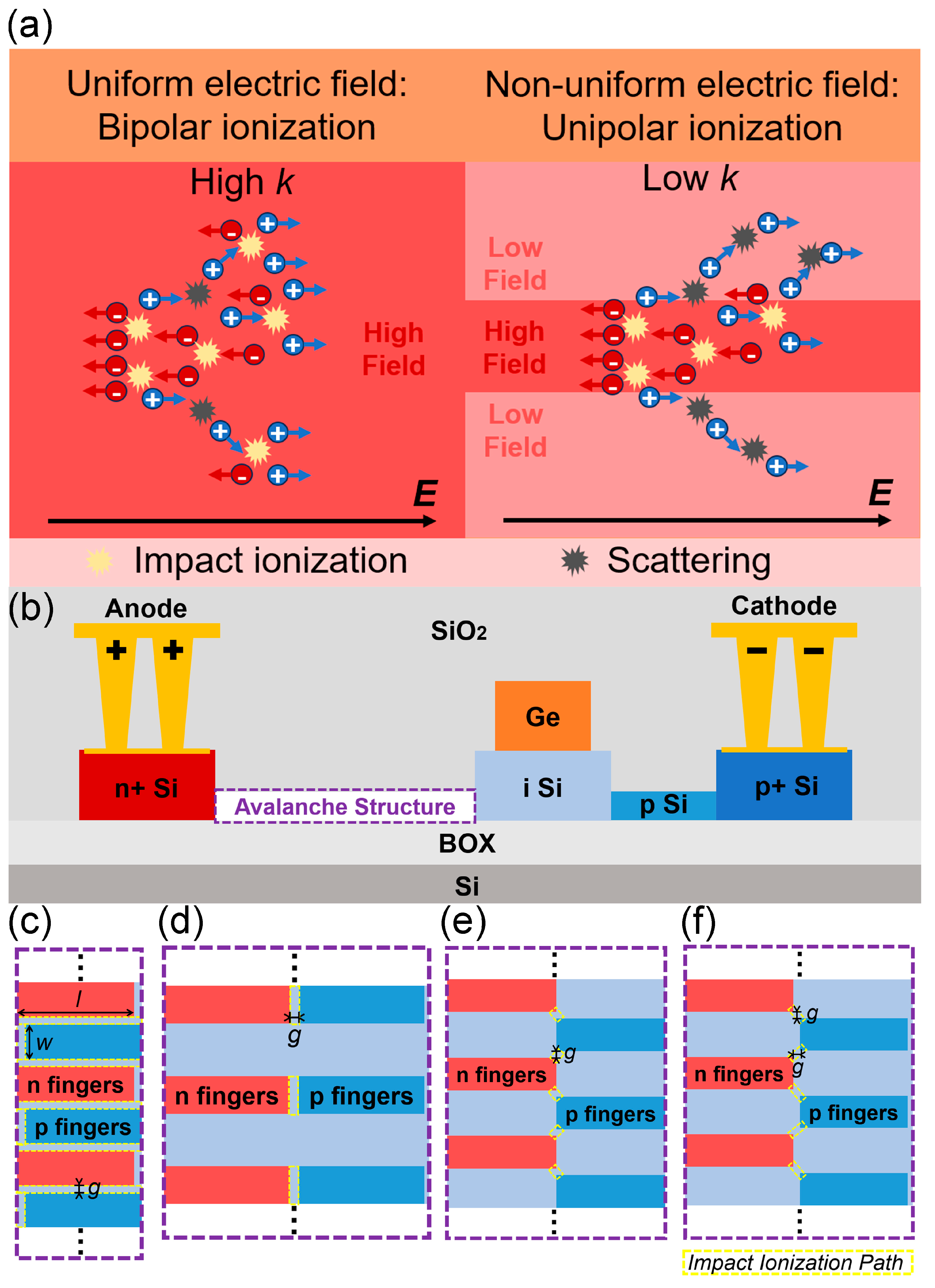
The holes have a much higher scattering rate than electrons in Si due to distinct scattering mechanisms; as a result, the mean free path (MFP) values of electrons are much longer than those of holes [19,20]. Compared with electrons, holes are easier to change in terms of their traveling directions. The operation principle of SE APD is shown in Figure 1a. In order to remove the bipolar ionization effect in the uniform electric field profile of conventional APDs, this work proposes a non-uniform profile design, wherein holes in the high-field region can be easily scattered into the low-field transport path without triggering ionizations, while electrons experience ballistic-like ionizations in the high-field region. The designed length of the high-field region should be longer than the hole MFP (generally above 10 nm) and, at the same time, its width should be short enough (narrower than the length) to secure the hole’s outward scattering.
Figure 1.
Introduction to device operational principles and optimized structural design. (a) The electric field distribution shifts from the original uniform state to a non-uniform pattern due to doping. In high-field regions, electrons exhibit a longer MFP, enabling high-efficiency impact ionization multiplication. Meanwhile, holes, with their shorter MFP, are scattered into low-field regions for transportation and collection. This approach enhances the unipolar ionization effect and reduces the k-value. (b) The cross-section schematic diagram of the four designed APDs, of which the vertical views of the avalanche structures (purple dashed rectangle) are shown in (c) APD1 with finger-insertion doping profile, (d) APD2 with finger-to-finger doping profile, (e) APD3 with 1D staggered-fingers doping profile, and (f) APD4 with 2D staggered-fingers doping profile. In all structures, l = 950 nm, w = 300 nm, and g = 100 nm. The parameter g denotes the edge-to-edge spacing between adjacent p- and n-doped fingers. For APD4, both the longitudinal and lateral spacings are equal to g. The parameter g affects the length and width of ionization path and SE efficiency. The Ge absorber has a width of 500 nm and a height of 260 nm. The Si waveguide connecting to the APDs is 450 nm in width and 220 nm in thickness. The Si rib width is 700 nm and the thickness is 220 nm/70 nm. All APDs’ length is 50 μm. The expected impact ionization path is denoted by yellow rectangles.
To validate the concept of SE APD, four Ge/Si waveguide APDs are designed and fabricated, namely APD1, APD2, APD3, and APD4, in the following discussion. These devices have a similar cross-sectional structure to that schematically depicted in Figure 1b, yet the planar doping profiles in avalanche structures are different, as can be seen in Figure 1c–f. The devices are designed as a separated-absorption-multiplication (SAM) structure to eliminate the influence of photogenerated holes; a rib structure is employed to minimize the electric field in the Ge absorber, which is prone to tunneling due to its narrow bandgap of 0.67 eV [21].
APD1 is designed to compare with other APDs using scattering-engineering optimization; the avalanche structure exhibits finger-insertion-type characteristics, which have been shown to offer low-operating-voltage advantages [22]. The high-field active avalanche area is expected to be in the intrinsic gap between n and p fingers, and there is no distinctive electron and hole path. For APD2, the scattering-engineering structure is introduced. A high-field electron ionization path is expected to be in the narrow intrinsic gap between n and p fingers, where holes could be scattered into both sides of the finger pairs, where the field is lower, to form a hole transport path. The doping finger width is 300 nm and cannot be reduced further. As a result, the electron ionization path width in APD2 is much longer than the MFP of holes, preventing an efficient scatter out of the holes and into the transport path. Therefore, APD3 and APD4 are designed; the n and p fingers are staggered in the longitudinal direction for APD3 and both longitudinal and horizontal directions for APD4 to form a narrower high-field electron ionization path between the corners of the n and p fingers. The designs and intended outcomes of the above APDs are briefly given in Table 1 for ready reference. Here, “1D” and “2D” refer to the number of in-plane directions in which p- and n-doped fingers are staggered. This geometrical distinction is reflected in the dimensionality of the high-field impact-ionization path: in APD3, longitudinal staggering produces a longitudinal impact-ionization path, while in APD4, a more oblique path, with components in both in-plane directions, is shaped due to the 2D staggered doping structure. The oblique path in APD4 is expected to form a longer and narrower high-field region that could achieve better performance. All fingers are heavily doped to confine the electric field and better investigate the properties of the avalanche area, which comes with the price of full depletion becoming a challenge and with a low field inside or below the Ge absorption region that could severely diminish the internal quantum efficiency (iQE) and the response speed. However, the noise analysis and k-value test could better reveal the properties of the novel avalanche structures, since the influence of avalanche within and below the Ge absorber is excluded. Further reducing the doping finger length or doping level could improve the iQE and the response speed.
Table 1.
Avalanche region designs and intended functions of the proposed APDs.
3. Results
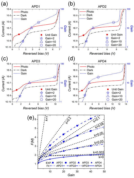
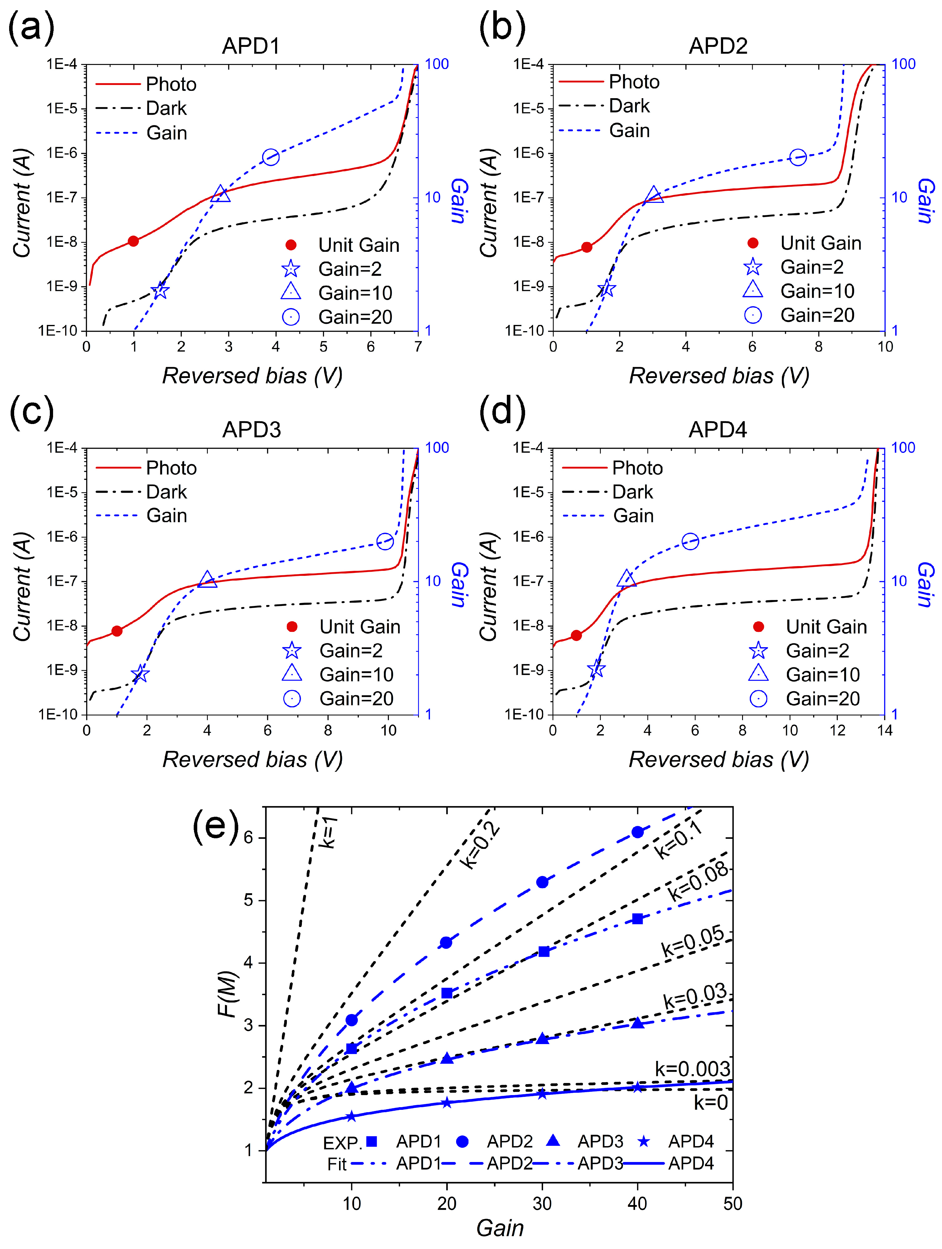
The room-temperature I–G–V experiments are carried out to investigate the operating voltages of each APD, as shown in Figure 2a–d. The avalanche gain is calculated per the following equation:
Figure 2.
The I–G–V curve of (a) APD1, (b) APD2, (c) APD3, and (d) APD4 at room temperature under the incident power of −30 dBm at 1550 nm. The black dashed dot curves and the red solid curves denote dark current and photocurrent, following the left axis. The blue dashed curves denote the avalanche gain, following the right axis. The unit gain point is identified as 1 V and highlighted by red dots (this is observed by the temperature-dependent measurement and will be described later). The representative gain points are denoted by star (gain = 2), triangle (gain = 10), and circle symbols (gain = 20). (e) The F–gain curve of APD1–4 compared with McIntyre’s local field model. The black dashed lines represent the F–gain curve of different k-values in the local field model. The symbols denote the experimental results, and the blue lines are the fitting results based on the experimental results. APD4 exhibits the best low k-value merit.
I and Id are the total current and dark current at a specific bias voltage, and I1 and Id1 are the total current and the dark current at the unit gain point, which is 1 V for each device in this work. The unit gain point of 1 V is further confirmed by the temperature-dependent G–V test in following discussions. Each device starts to avalanche when the reverse bias exceeds 1 V and can achieve a prominent gain at a reverse bias of only ~2 V. The gain curves of APD2, APD3, and APD4 experience a rapid rise at 2–4 V reverse bias, then climb slowly at higher bias. This is because the MFP of electrons drastically decreases at higher bias due to the increasing energy, and part of the electrons can be scattered into the low-field transport region, thereby diminishing the avalanche gain in SE APD. In Figure S2 (Supplementary Material), as the incident power increases from −30 dBm to −16 dBm, the maximum gain of all APDs drops by one order of magnitude. This phenomenon is attributed to carrier scattering and the space charge effect and has been observed in many reports [13,23]. For waveguide Ge/Si APD, incident photons are always mostly absorbed in the initial several micrometers of the absorber, which would cause high carrier density in APD, enhancing the space charge effect and the carrier scattering. Therefore, further absorber designs achieving uniform photon absorption could lower the carrier density and extend the dynamic range of the device; for example, distributed Bragg reflector or slow-light structures can be introduced into the absorber to form more uniform resonant incident power distribution and further achieve uniform photon absorption. Carrier density in an avalanche region could be further decreased by adopting thicker top Si to improve the dynamic range performance. Additionally, the responsivity (R@1550 nm) at unit gain for APD1–4 is ~0.01 A/W; R could reach 1.28 A/W, 0.99 A/W, 1.22 A/W, and 1.43 A/W near breakdown point. The low unit gain quantum efficiency (QE) ~0.8% could be attributed to two major causes: Firstly, the rib structure decreases the coupling efficiency between the waveguide and the APD devices if the coupling taper is not optimized, meaning that the photon absorption rate could be severely reduced. Secondly, photogenerated electrons diffuse under the Ge absorber and inside the p fingers, meaning that the iQE can be low due to the recombination of photogenerated electrons. It is calculated that the iQE in this work is about 78%, considering the minor electron diffusion length Le of ~8 μm (Supplementary Material). Therefore, it is believed that the photon absorption rate (~1%) is the chief factor limiting the QE. Furthermore, 473 nm normal incident I–G–V tests have been carried out as shown in Figure S5 (Supplementary Material). The avalanche still occurs at only ~2 V with measured iQE around 40–60% for the proposed APDs, indicating that QE is limited by the photon absorption rate due to the low waveguide coupling efficiency, which can be improved by optimizing the waveguide coupling structure in the future. Further optimization of the taper design and the proper lower finger doping level could be expected to greatly improve the SE APD performance. The addition of reflectors or slow-light structure could also improve the photon absorption rate.
The dark current of APD1 is the highest at relatively high gain, nearly saturating the photocurrent and potentially resulting in a low signal-to-noise ratio and degraded sensitivity. The gain points of 2 for APD1, APD2, APD3, and APD4 are 1.56 V, 1.61 V, 1.78 V, and 1.84 V, respectively. The gain points of 20 are 3.9 V, 7.4 V, 9.9 V, and 5.8 V, indicating the best low-operating-voltage property of APD4 among the three SE APDs. The operating voltage of APD1 is slightly lower, yet the k-value is a lot higher, as will be discussed later. The breakdown voltages for APD1, APD2, APD3, and APD4 are about 6.5 V, 8.5 V, 10.5 V, and 13 V, respectively; the increasing trend is attributed to the increasing avalanche path length and the scattering mechanism. A shorter avalanche path is associated with a lower breakdown voltage and a higher electric field under given gain [24], and the holes’ scattering efficiency increases from APD1 to APD4, which means the hole ratio contributing to avalanche is decreasing. As a result, higher voltage could be expected for APD2–4 to realize breakdown, which is a bipolar ionization-induced phenomenon. At breakdown points, the peak electric fields for APD1, APD2, APD3, and APD4 are 450 kV/cm, 490 kV/cm, 470 kV/cm, and 460 kV/cm according to TCAD simulations.
To investigate the noise performance and k-value of each APD device, NPSD experiments at different gain values are carried out. The total noise results of APD1 to APD4 are presented in Figure S3a–d (Supplementary Material). The photocurrent at unit gain is calibrated as 25 nA for APD1 and 50 nA for APD2, APD3, and APD4. Hence, a direct comparison of the NPSD of these APDs is reasonable. The total noise of all devices is about −102 dBm/Hz at unit gain. The total noise of APD1, APD2, APD3, and APD4 climbs to −94 dBm/Hz, −94.5 dBm/Hz, −96.8 dBm/Hz, and −97.3 dBm/Hz at a gain of 40. The total noise at other gain values drops from APD1 to APD4 as well, indicating the best low-noise merit of APD4.
The k-value of each APD device can be extracted from the NPSD results by calculating the excess noise factor F(M) per the following equation [25]:
M is the avalanche gain and ks is the linear fit slope of the net noise versus M in log-log plot. Net noise, which equals the total noise minus the dark noise, can be deemed as excess noise . As is shown in Figure S4 (Supplementary Material), ks of APD1, APD2, APD3, and APD4 are 2.42, 2.49, 2.30, and 2.19, respectively. By plotting the calculated F(M) in reference to McIntyre’s model curves corresponding to different k-values, as Figure 2e displays, the k-value of each APD device can be obtained. It is more reasonable to compare the results with McIntyre’s model over a higher-gain range to extract the k-value for each APD, given the mismatch between the experiments and the model at the lower-gain range. This mismatch is commonly reported in low-noise APD structures, suppressing impact ionization of specific carriers, such as in digital-alloy APDs [26,27,28]. The k-values for APD1, APD2, APD3, and APD4 are approximately 0.08, 0.12, 0.03, and 0.003, respectively. In general, the k-value decreases as the holes’ scattering efficiency increases, which suggests that the concept of SE APD is functional. APD4 exhibits the lowest total noise and k-value and the electron unipolar ionization is deemed to be achieved.
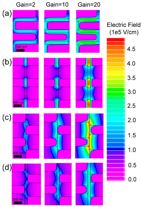
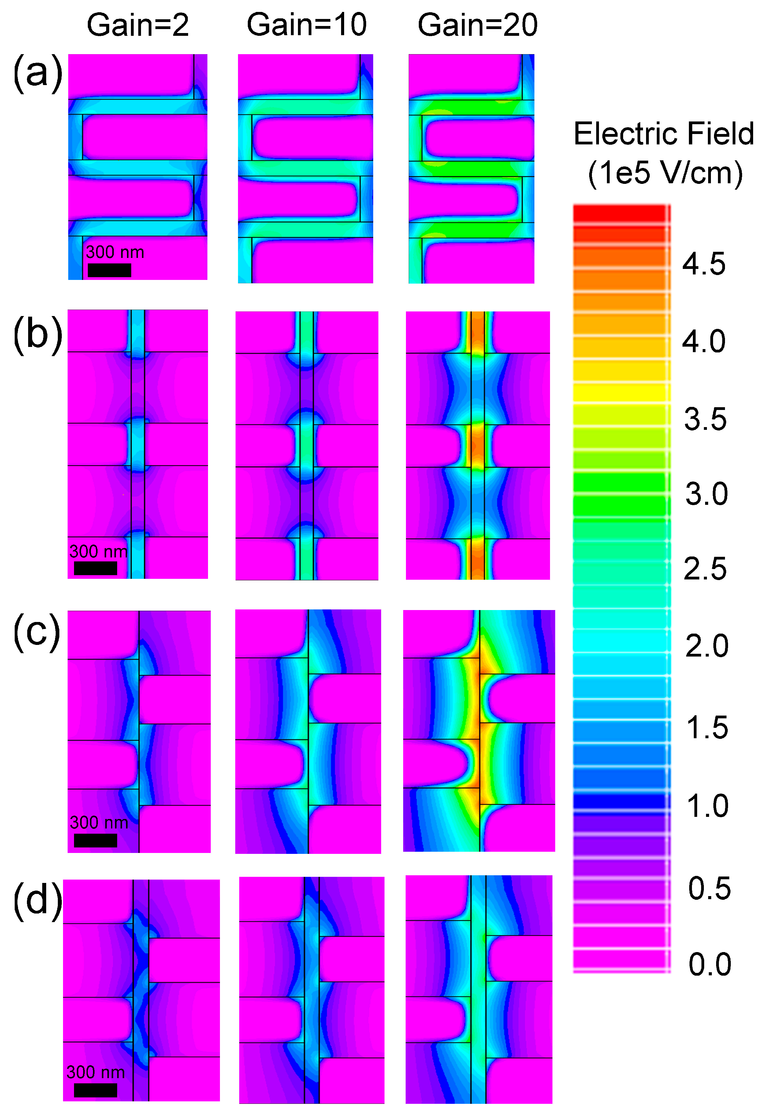
To better understand the carrier behavior in APD1 to APD4 and provide deeper insights for the k-value results, the electric fields in the avalanche structure for each APD corresponding to gain points of 2, 10, 20 denoted in Figure 2a–d are illustrated in Figure 3. The electric field for the entire devices can be seen in Figure S10 (Supplementary Material); the electric field is mainly concentrated in the avalanche regions. The electric field in APD1 mainly concentrates in the gaps between the fingers, forming a compact avalanche structure, and there is no distinctive electron or hole path. The electric field in APD2 forms a high-field electron ionization path between fingers and a low-field hole transport path on both sides of the avalanche path. The electric field in APD3 and APD4 forms a narrow electron ionization path. At any gain point, the width of the high-field ionization path in APD4 is the narrowest, which could better scatter the hole into the low-field transport path. Furthermore, the electric field in APD4 is the lowest at all gain points, which is beneficial for electron ballistic-like ionization due to the longer MFP. At a gain of 20, the electric field in APD2/APD3 is the highest ~4.5 × 10⁵ V/cm, while that in APD4 is still the lowest ~2.5 × 10⁵ V/cm. This can also be seen in the energy bands along the ionization path for each APD in Figure S11 (Supplementary Material), where the slope of the bands is positively related to the electric field. These merits help achieve the extremely low k-value in APD4.
Figure 3.
The vertical view of the electric field at the bias of gain = 2, 10, 20 in the periodic avalanche structure unit in (a) APD1, (b) APD2, (c) APD3, (d) APD4. At each gain point, APD4 exhibits the narrowest high-field ionization path and the lowest electric field. These characteristics promote electron ballistic-like ionization while more effectively scattering holes into the low-field transport path, thereby resulting in a low k-value.
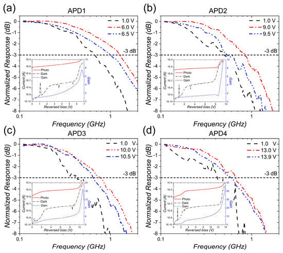
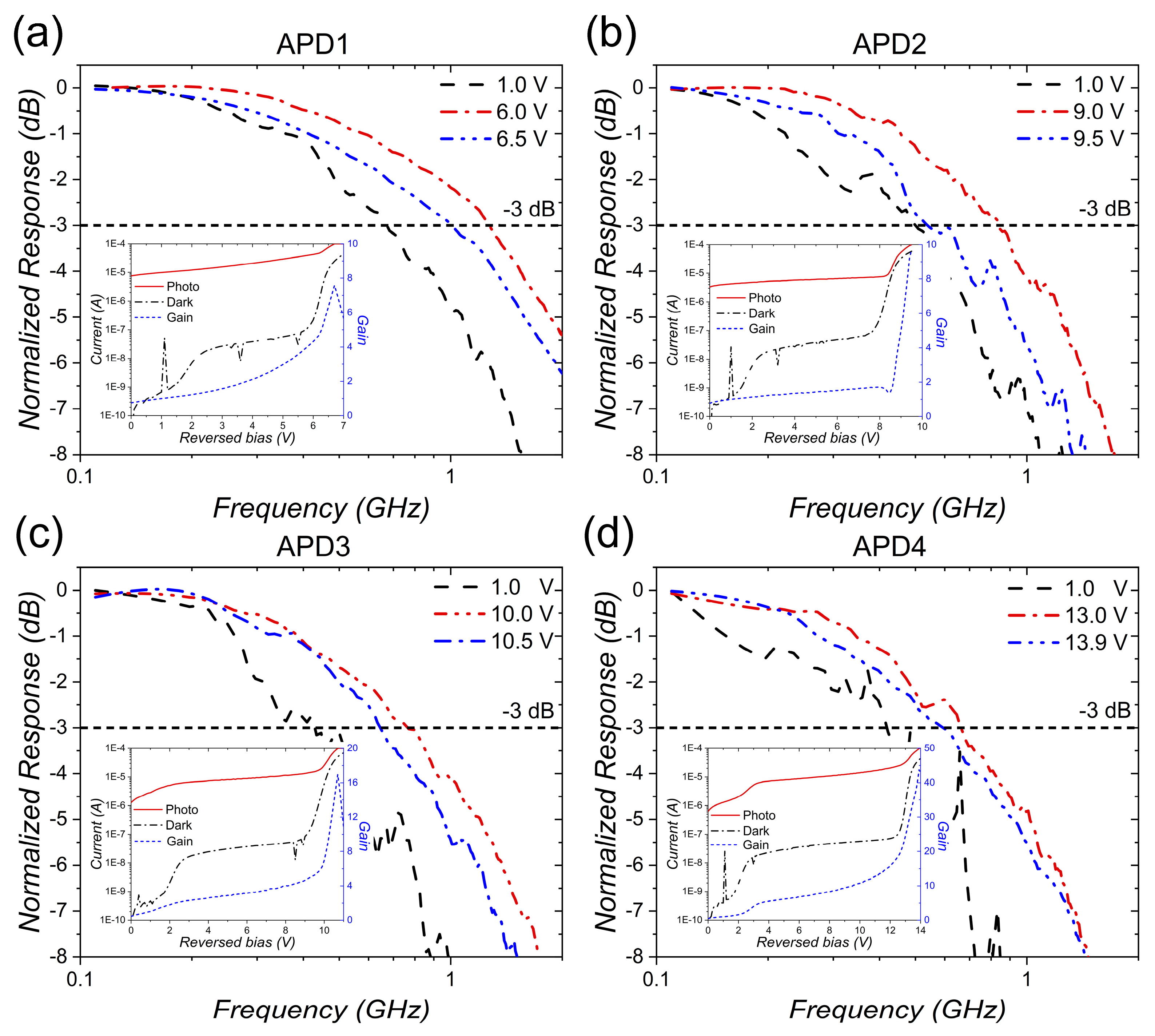
The frequency response experiments are carried out to estimate the 3 dB bandwidth and GBP performance of the APD devices, as shown in Figure 4. I–G–V curves for each APD under the same test conditions as those during the frequency response test are displayed in the insets, and the corresponding gain values are extracted to calculate GBP. Note that the incident power is set according to the minimum power that meets the test system sensitivity requirement for each APD. The 3 dB bandwidth of all APDs increases and decreases as bias climbs. The increasing trend is due to improved carrier transport efficiency and a reduced RC constant, attributed to the longer depletion area, while the decreasing trend is due to the increasing avalanche buildup time at high bias voltage and high gain. The bandwidths at the highest gain points for APD1, APD2, APD3, and APD4 are 1.0 GHz, 0.6 GHz, 0.65 GHz, and 0.63 GHz, respectively. The highest GBP values for APD1, APD2, APD3, and APD4 are 6 GHz, 6 GHz, 9.1 GHz, and 28 GHz. Further increasing bias voltage could induce device failure. The superior GBP performance of APD4, together with the lowest incident power that meets the system sensitivity, could also hint at a low k-value. A theoretical model simulating the frequency response of APDs at unit gain points in this work has been established as depicted in Figures S6 and S7 (Supplementary Material); similar analytic models have been developed in other reports [29]. Due to the lack of core fabrication parameters such as doping concentration from the foundry, the active region of the designed p-i-p-i-n APDs in this paper is not fully depleted. Photogenerated carriers can barely experience electric field, and thus only move via diffusion scheme in the undepleted region, resulting in a slow speed that severely impacts bandwidth. The simulations indicate that, by completely depleting the active region, the APD bandwidth can be improved from the present sub-GHz level to approximately 20–30 GHz. This can be optimized by lowering the doping or by shortening the finger length of APDs in this work; properly moving avalanche structures below the Ge absorber could also work.
Figure 4.
The frequency response experiments under incident of 1550 nm of (a) APD1@~0 dBm, (b) APD2@~−3 dBm, (c) APD3@~−5 dBm, and (d) APD4@~−7 dBm at different reverse bias voltages. The I–G–V curves under the same test conditions are exhibited in the insets. By optimizing the scattering-engineering structure, the GBP is improved by approximately fivefold from 6 GHz in APD1 to 28 GHz in APD4.
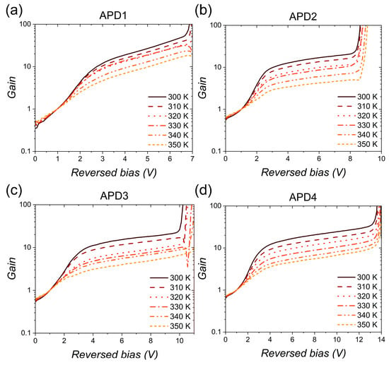
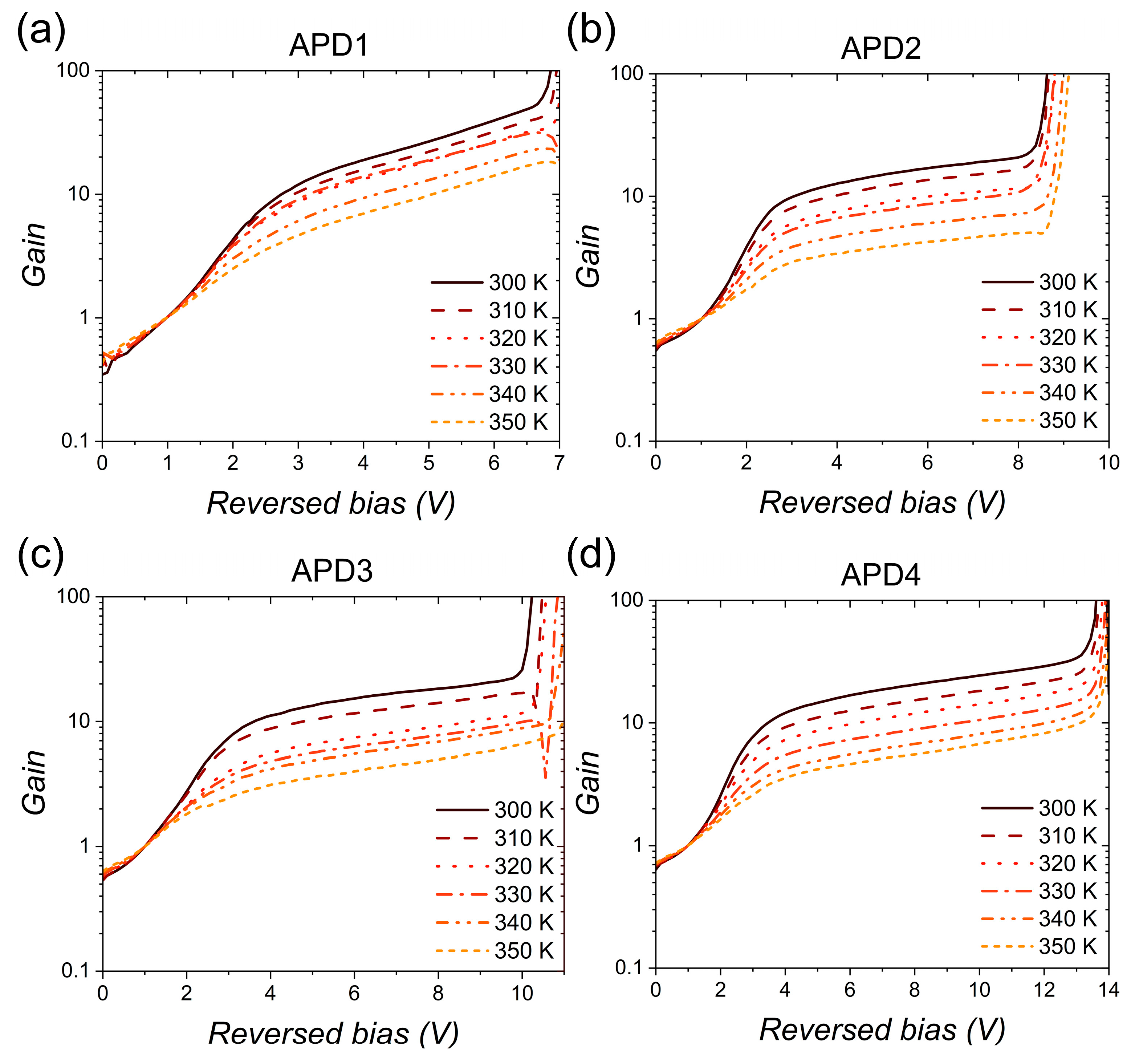
The temperature-dependent G–V experiments from 300 K to 350 K are carried out for all APD devices to verify the avalanche nature of gain as is depicted in Figure 5. The G–V curves become strongly temperature-dependent above 1 V, indicating that the unit gain point is approximately 1 V. It turns out that the avalanche gain of all APD devices declines as temperature increases; the negative relationship between gain value and temperature could thus provide solid evidence for the avalanche nature of the observed gain, because the phonon-assisted scattering hindering impact ionization is enhanced as the temperature climbs. The temperature drift coefficient of the breakdown voltage is estimated to be 12 mV/K, 10 mV/K, 18 mV/K, and 9 mV/K, which are relatively low values compared with the 5–50 mV/K that have been reported in studies regarding Ge/Si or III–V APD [4,30], showing good temperature stability. Furthermore, the dark current of each APD increases with rising temperature, as shown in Figure S8 (Supplementary Material), which is attributed to the thermally generated dark current. It is estimated that minor electron diffusion length changes from ~8 μm at 300 K to ~7 μm at 350 K in this work (Supplementary Material) [31,32,33], causing 4% decrease in iQE given the diffusion path length of ~2 μm in APDs, which cannot evidently influence the gain curve. In addition, the forward I–V curves in Figure S9 (Supplementary Material) exhibit conductivity characteristics for all APDs in this work, further indicating the avalanche nature of the gain instead of photoconductive gain.
Figure 5.
The temperature-dependent G–V curves from 300 K to 350 K under the incident power of −30 dBm at 1550 nm for (a) APD1, (b) APD2, (c) APD3, (d) APD4. The G–V curves become strongly temperature-dependent above 1 V, indicating that the unit gain point is approximately 1 V. The negative relationship between gain value and temperature could thus provide solid evidence for the avalanche nature of the observed gain; the temperature drift coefficient of the breakdown voltage is estimated to be 12 mV/K, 10 mV/K, 18 mV/K, and 9 mV/K.
4. Discussion
Table 2 compares the typical characteristics of the best-optimized SE APD (APD4) in this work with those of previously reported APD devices. The breakdown voltage, extracted k-value, voltage at gain of 10 and corresponding incident power are summarized. These results suggest that the scattering-engineering method provides a promising approach to achieving low-noise avalanche multiplication while maintaining low operating voltage and dark current. It is noteworthy that, in a recent simulation report, gate-assisted electric-field modulation has also been investigated, predicting a low breakdown voltage of −0.8 V in a gated InGaAs APD through control of the electric field [34].
Table 2.
Comparison of key performance parameters of the proposed SE APD and previously reported APDs.
It is important to declare that although the function of SE APD is realized via Ge/Si waveguide structure in this work, the SE mechanism could also be applied to APD fabricated on other material platforms like III–V APD, and even better outcomes can be expected in materials exhibiting larger difference between the MFP of electrons and holes.
Circuit modeling for SE APDs could be helpful in optimizing the bandwidth performance utilizing similar models in previous reports [41]. However, the staggered-finger structures produce spatially non-uniform electric fields, with localized high-field multiplication paths coupled to surrounding low-field transport regions. Their spatial extent evolves with bias, raising the difficulty of circuit modeling. Therefore, a quantitatively validated circuit model remains an important direction for future work.
Modeling the avalanche gain or excess noise in APD is also a significant direction; the proposed SE APD could, in principle, be investigated using Monte Carlo simulations, where the two-dimensional carrier transport and scattering processes shall be explicitly taken into consideration. By contrast, existing random path length (RPL) and recurrence models are primarily developed for conventional APDs with one-dimensional multiplication regions, in which carrier transport and scattering are incorporated in a simplified statistical manner to improve computational efficiency. Extending these models to the proposed SE APD would require substantial modifications to account for the two-dimensional carrier transport and scattering mechanisms. Therefore, Monte Carlo simulations would likely provide a more appropriate framework for investigating the physical mechanism of the proposed SE APD in future work.
5. Conclusions
In conclusion, SE APD is proposed and validated to reduce the operating voltage while maintaining low excess noise. In SE APD, an avalanche occurs at a low reverse bias of ~2 V under an incident of −30 dBm at 1550 nm. An extremely low k-value of 0.003 is achieved in the best-optimized SE APD. The best-optimized SE APD requires the lowest electric field to achieve a given gain. By optimizing the scattering-engineering structure, the GBP is improved by about fivefold from 6 GHz to 28 GHz. The avalanche nature is proved by the temperature-dependent gain–voltage test, and a low breakdown-voltage temperature-drift coefficient of ~10 mV/K, representing good thermal stability, is obtained.
Supplementary Materials
The following supporting information can be downloaded at https://www.mdpi.com/article/10.3390/photonics13111069/s1. Figure S1: The schematic diagram of the noise power spectral density test system; Figure S2: The G-V curves of (a) APD1, (b) APD2, (c) APD3, (d) APD4 under the incident of the 1550 nm laser of different power; Figure S3: The noise power spectral density under gain ranging from 1 to 40 of (a) APD1, (b) APD2, (c) APD3, (d) APD4; Figure S4: The slope of the net noise versus M in log-log plot ks of (a) APD1, (b) APD2, (c) APD3, (d) APD4; Figure S5: The I-G-V test of (a) APD1, (b) APD2, (c) APD3, (d) APD4 under normal incident of 473 nm; Figure S6: The experiment and simulated frequency response under unit gain@1 V of (a) APD1, (b) APD2, (c) APD3, (d) APD4; Figure S7: The simulated frequency response components under unit gain@1 V of (a) APD1, (b) APD2, (c) APD3, (d) APD4; Figure S8: The temperature dependent dark current results of (a) APD1, (b) APD2, (c) APD3, (d) APD4; Figure S9: The forward bias I-V curves of APDs in this work; Figure S10: The electric field in entire devices in this work at gain of 20: (a) APD1, (b) APD2, (c) APD3, (d) APD4; Figure S11: Energy band diagram along the impact ionization path at gain of 20 for (a) APD1, (b) APD2, (c) APD3, (d) APD4.
Author Contributions
B.L.: Data curation (lead); writing—original draft (lead); conceptualization (supporting); methodology (equal); formal analysis (lead); validation (lead); visualization (lead); writing—review and editing (supporting). J.Z.: Supervision (equal); writing—review and editing (lead); project administration (lead); conceptualization (lead); methodology (equal); funding acquisition (lead). G.L.: Methodology (equal); writing—review and editing (supporting). T.W.: Methodology (equal); writing—review and editing (supporting). A.G.: Methodology (equal); writing—review and editing (supporting). L.W.: Methodology (equal); data curation (supporting). Z.H.: Methodology (equal); formal analysis (supporting). B.X.: Methodology (equal); validation (supporting). C.S.: Methodology (equal); formal analysis (supporting). Y.L.: Methodology (equal); supervision (equal). All authors have read and agreed to the published version of the manuscript.
Funding
The authors acknowledge the National Natural Science Foundation of China (Grant Nos. T2322016, 62235011), the National Key Laboratory of Laser Spatial Information Foundation (Grant No. LSI2024JCKY03), the Beijing Municipal Science & Technology Commission, the Administrative Commission of Zhongguancun Science Park (Z241100004224016), the Centre of Nanofabrication (Tsinghua University), and the Collaborative Innovation Center of Solid-State Lighting and Energy-Saving Electronics.
Data Availability Statement
The original data presented in the study are openly available in FigShare at https://doi.org/10.6084/m9.figshare.34420527.
Acknowledgments
The authors acknowledge the SiFotonics company for their RF frequency response test environment.
Conflicts of Interest
Author Anran Guo was employed by the CETC Chips Technology Group Co., Ltd. The remaining authors declare that the research was conducted in the absence of any commercial or financial relationships that could be construed as a potential conflict of interest. The funders had no role in the design of the study; in the collection, analyses, or interpretation of data; in the writing of the manuscript; or in the decision to publish the results.
Abbreviations
The following abbreviations are used in this manuscript:
| APD | Avalanche photodiode |
| PD | Photodiode |
| GBP | Gain–bandwidth product |
| SE APD | Scattering-engineered APD |
| I–G–V | Current–gain–voltage |
| NPSD | Noise power spectral density |
| k-value | Impact ionization coefficient ratio |
| SAM | Separated-absorption-multiplication |
| MFP | Mean free path |
| iQE | Internal quantum efficiency |
References
- Kodati, S.H.; Lee, S.; Guo, B.; Jones, A.H.; Schwartz, M.; Winslow, M.; Pfiester, N.A.; Grein, C.H.; Ronningen, T.J.; Campbell, J.C.; et al. AlInAsSb avalanche photodiodes on InP substrates. Appl. Phys. Lett. 2021, 118, 091101. [Google Scholar] [CrossRef] [Scilit]
- Zhao, Y. Recent advances of infrared avalanche photodiodes based on low-noise aluminum (antimony)-contained materials and their journey toward single-photon detection. APL Photonics 2026, 11, 041201. [Google Scholar] [CrossRef] [Scilit]
- Soroosh, M.; Moravvej-Farshi, M.K.; Saghafi, K. A simple empirical model for calculating gain and excess noise in GaAs/Al.XI.Ga1-.XI.As APDs (0.3.LEQ..XI..LEQ.0.6). IEICE Electron. Express 2008, 5, 853–859. [Google Scholar] [CrossRef] [Scilit]
- Liu, B.; Liu, Y.; Zhao, J.; Zheng, J.; Wu, R.; Yang, Y.; Hua, X.; Wang, X.; Guo, A.; Yu, B.; et al. Transforming photodiode into avalanche photodiode: An efficient method improving the sensitivity performance of foundry-fabricated Si/Ge receiver. J. Appl. Phys. 2025, 138, 064501. [Google Scholar] [CrossRef] [Scilit]
- Wang, S.; Ye, H.; Geng, L.; Chu, Y.; Zheng, Y.; Han, Q. High-Speed Planar InGaAs/InAlAs Avalanche Photodiode. IPTL 2025, 37, 235–238. [Google Scholar] [CrossRef] [Scilit]
- Yao, Y.; Zhang, L.; Yu, J.; Gao, J.; Huang, C.; Liu, Y.; Ma, R.; Zhang, N.; Hu, H.; Wang, L.; et al. Gate-Voltage Control of Waveguide-Coupled Lateral Ge-on-Si APD for 1550 nm Detection. IEEE Sens. J. 2024, 24, 38929–38934. [Google Scholar] [CrossRef] [Scilit]
- Nada, M.; Nakajima, F.; Yoshimatsu, T.; Nakanishi, Y.; Tatsumi, S.; Yamada, Y.; Sano, K.; Matsuzaki, H. High-speed III-V based avalanche photodiodes for optical communications—The forefront and expanding applications. Appl. Phys. Lett. 2020, 116, 140502. [Google Scholar] [CrossRef] [Scilit]
- Na, N.; Lu, Y.C.; Liu, Y.H.; Chen, P.W.; Lai, Y.C.; Lin, Y.R.; Lin, C.C.; Shia, T.; Cheng, C.H.; Chen, S.L. Room temperature operation of germanium-silicon single-photon avalanche diode. Nature 2024, 627, 295–300. [Google Scholar] [CrossRef] [Scilit] [PubMed]
- Liu, T.; Yang, G.; Li, J.; Tong, C. High-speed avalanche photodiodes for optical communication. Photonics Res. 2025, 13, 1438–1451. [Google Scholar] [CrossRef] [Scilit]
- Xue, J.; Cheng, C.; Bao, S.; Liu, Q.; Zhang, W.; Wang, B. High-speed Si-Ge avalanche photodiode with a gain-bandwidth product of 7564 GHz. Nat. Commun. 2026, 17, 3730. [Google Scholar] [CrossRef] [Scilit] [PubMed]
- McIntyre, R.J. Multiplication noise in uniform avalanche diodes. IEEE Trans. Electron Devices 1966, ED-13, 164–168. [Google Scholar] [CrossRef] [Scilit]
- Emmons, R.B. Avalanche-Photodiode Frequency Response. J. Appl. Phys. 1967, 38, 3705–3714. [Google Scholar] [CrossRef] [Scilit]
- Shi, Y.; Li, X.; Chen, G.; Zou, M.; Cai, H.; Yu, Y.; Zhang, X. Avalanche photodiode with ultrahigh gain–bandwidth product of 1,033 GHz. Nat. Photonics 2024, 18, 610–616. [Google Scholar] [CrossRef] [Scilit]
- Huang, M.; Li, S.; Cai, P.; Hou, G.; Su, T.-I.; Chen, W.; Hong, C.-Y.; Pan, D. Germanium on Silicon Avalanche Photodiode. IEEE J. Sel. Top. Quantum Electron. 2018, 24, 1–11. [Google Scholar] [CrossRef] [Scilit]
- Peng, Y.; Yuan, Y.; Sorin, W.V.; Cheung, S.; Huang, Z.; Hong, C.; Liang, D.; Fiorentino, M.; Beausoleil, R.G. An 8 × 160 Gb s−1 all-silicon avalanche photodiode chip. Nat. Photonics 2024, 18, 928–934. [Google Scholar] [CrossRef] [Scilit]
- Shi, Y.; Zou, M.; Li, Z.; Yu, Y.; Zhang, X. Ultrafast avalanche photodiode exceeding 100 GHz bandwidth. Nat. Commun. 2025, 16, 11058. [Google Scholar] [CrossRef] [Scilit] [PubMed]
- Wu, Y.-K.; Kuo, C.-C.; Lin, P.-S.; Yang, S.; Chen, H.S.; Huang, J.J.-S.; Shi, J.-W. Thinning of Cascaded Multiplication Layers in Avalanche Photodiodes for High-Speed and High-Power-Tolerant Performance. J. Light. Technol. 2025, 43, 690–700. [Google Scholar] [CrossRef] [Scilit]
- Ahmad, Z.; Wang, P.-S.; Naseem; Huang, Y.-C.; Chang, Y.-C.; Chang, Y.-C.; Lee, Y.-S.; Shi, J.-W. Avalanche photodiodes with multiple multiplication layers for coherent detection. Sci. Rep. 2022, 12, 16541. [Google Scholar] [CrossRef] [Scilit] [PubMed]
- Qiu, B.; Tian, Z.; Vallabhaneni, A.; Liao, B.; Mendoza, J.M.; Restrepo, O.D.; Ruan, X.; Chen, G. First-principles simulation of electron mean-free-path spectra and thermoelectric properties in silicon. EPL (Europhys. Lett.) 2015, 109, 57006. [Google Scholar] [CrossRef] [Scilit]
- Li, Z.; Graziosi, P.; Neophytou, N. Deformation potential extraction and computationally efficient mobility calculations in silicon from first principles. Phys. Rev. B 2021, 104, 195201. [Google Scholar] [CrossRef] [Scilit]
- Virot, L.; Crozat, P.; Fédéli, J.-M.; Hartmann, J.-M.; Marris-Morini, D.; Cassan, E.; Boeuf, F.; Vivien, L. Germanium avalanche receiver for low power interconnects. Nat. Commun. 2014, 5, 4957. [Google Scholar] [CrossRef] [Scilit] [PubMed]
- Zeng, X.; Huang, Z.; Wang, B.; Liang, D.; Fiorentino, M.; Beausoleil, R.G. Silicon–germanium avalanche photodiodes with direct control of electric field in charge multiplication region. Optica 2019, 6, 772–777. [Google Scholar] [CrossRef] [Scilit]
- Pang, Y.; Liu, Z.; Zhu, Y.; Liu, X.; Zhang, D.; Niu, C.; Li, M.; Zheng, J.; Zuo, Y.; Cheng, B. High-performance waveguide-coupled lateral Ge/Si avalanche photodetector. Opt. Lett. 2022, 47, 4463–4466. [Google Scholar] [CrossRef] [Scilit] [PubMed]
- Goh, Y.L.; Massey, D.J.; Marshall, A.R.J.; Ng, J.S.; Tan, C.H.; Ng, W.K.; Rees, G.J.; Hopkinson, M.; David, J.P.R.; Jones, S.K. Avalanche Multiplication in InAlAs. IEEE Trans. Electron Devices 2007, 54, 11–16. [Google Scholar] [CrossRef] [Scilit]
- Wang, Q.; Ma, Y.; Liu, B.; Xia, R.; Zhang, G.; Gu, Y.; Li, X. Planar InGaAs Avalanche Photodiode With Multi-Stage InAlAs/InAlGaAs Multiplication Structure. IEEE J. Quantum Electron. 2025, 61, 1–6. [Google Scholar] [CrossRef] [Scilit]
- Sheridan, B.; Collins, X.; Taylor-Mew, J.; White, B.; Ng, J.S.; Tan, C.H. An Extremely Low Noise-Equivalent Power Photoreceiver Using High-Gain InGaAs/AlGaAsSb APDs. J. Light. Technol. 2025, 43, 741–746. [Google Scholar] [CrossRef] [Scilit]
- Zheng, J.; Yuan, Y.; Tan, Y.; Peng, Y.; Rockwell, A.K.; Bank, S.R.; Ghosh, A.W.; Campbell, J.C. Digital Alloy InAlAs Avalanche Photodiodes. J. Light. Technol. 2018, 36, 3580–3585. [Google Scholar] [CrossRef] [Scilit]
- Shahnewaz, S.; Karimi, H.; Campbell, J.C.; Ghosh, A.W.; Osiński, M.; Arakawa, Y.; Grillot, F. A full-band Monte Carlo framework for explaining sub-McIntyre excess noise in Sb-based avalanche photodiodes. In Proceedings of the Physics and Simulation of Optoelectronic Devices XXXIV, San Francisco, CA, USA, 17–23 January 2026. [Google Scholar]
- Loquai, S.; Bunge, C.-A.; Ziemann, O.; Schmauss, B.; Kruglov, R. A Fully Analytic Model of Large Area Silicon p-i-n Photodiodes Verified at Short Wavelengths. J. Light. Technol. 2010, 28, 2646–2653. [Google Scholar] [CrossRef] [Scilit]
- Guo, B.; Ahmed, S.Z.; Xue, X.; Rockwell, A.-K.; Ha, J.; Lee, S.; Liang, B.; Jones, A.H.; McArthur, J.A.; Kodati, S.H.; et al. Temperature Dependence of Avalanche Breakdown of AlGaAsSb and AlInAsSb Avalanche Photodiodes. J. Light. Technol. 2022, 40, 5934–5942. [Google Scholar] [CrossRef] [Scilit]
- Tyagi, M.S.; Van Overstraeten, R. Minority Carrier Recombination in Heavily-Doped Silicon. Solid-State Electron. 1983, 26, 577–597. [Google Scholar] [CrossRef] [Scilit]
- Mathur, P.C.; Sharma, R.P.; Saxena, P.; Arora, J.D. Temperature dependence of minority carrier lifetime in single-crystal and polycrystalline Si solar cells. J. Appl. Phys. 1981, 52, 3651–3654. [Google Scholar] [CrossRef] [Scilit]
- Würfel, P.; Trupke, T.; Puzzer, T.; Schäffer, E.; Warta, W.; Glunz, S.W. Diffusion lengths of silicon solar cells from luminescence images. J. Appl. Phys. 2007, 101, 123110. [Google Scholar] [CrossRef] [Scilit]
- Sharafi, F.; Alaei-Sheini, N.; Soroosh, M. Design and simulation of the avalanche photodiode utilizing field effect diode structure to decrease excess noise and improve detectivity. Results Opt. 2026, 24, 101074. [Google Scholar] [CrossRef] [Scilit]
- Nada, M.; Yamada, Y.; Matsuzaki, H. Responsivity-Bandwidth Limit of Avalanche Photodiodes: Toward Future Ethernet Systems. IEEE J. Sel. Top. Quantum Electron. 2018, 24, 1–11. [Google Scholar] [CrossRef] [Scilit]
- Yi, X.; Xie, S.; Liang, B.; Lim, L.W.; Cheong, J.S.; Debnath, M.C.; Huffaker, D.L.; Tan, C.H.; David, J.P.R. Extremely low excess noise and high sensitivity AlAs0.56Sb0.44 avalanche photodiodes. Nat. Photonics 2019, 13, 683–686. [Google Scholar] [CrossRef] [Scilit]
- Hu, X.; Zhang, H.; Wu, D.; Chen, D.; Wang, L.; Xiao, X.; Yu, S. High-performance germanium avalanche photodetector for 100 Gbit/s photonics receivers. Opt. Lett. 2021, 46, 3837–3840. [Google Scholar] [CrossRef] [Scilit] [PubMed]
- Yanikgonul, S.; Leong, V.; Ong, J.R.; Hu, T.; Siew, S.Y.; Png, C.E.; Krivitsky, L. Integrated avalanche photodetectors for visible light. Nat. Commun. 2021, 12, 1834. [Google Scholar] [CrossRef] [Scilit] [PubMed]
- Cao, H.; Xie, J.; Xiang, Y.; Sun, W.; Tang, L.; Wang, X.; Chen, W.; Guo, J.; Zhang, G.; Shi, Y.; et al. Impact-ionization-engineered waveguide Ge/Si avalanche photodiode with a record-high gain-bandwidth product of 5580 GHz. PhotoniX 2026, 7, 45. [Google Scholar] [CrossRef] [Scilit]
- Xiang, Y.; Cao, H.; Liu, C.; Guo, J.; Dai, D. High-speed waveguide Ge/Si avalanche photodiode with a gain-bandwidth product of 615 GHz. Optica 2022, 9, 762–769. [Google Scholar] [CrossRef] [Scilit]
- Abbas Zarifkar, M.S. Circuit Modeling of Separate Absorption, Charge and Multiplication Avalanche Photodiode (Sacm-Apd). In Proceedings of the 6th International Conference on Laser and Fiber-Optical Networks Modeling, Kharkiv, Ukraine, 6–9 September 2004. [Google Scholar]

Disclaimer/Publisher’s Note: The statements, opinions and data contained in all publications are solely those of the individual author(s) and contributor(s) and not of MDPI and/or the editor(s). MDPI and/or the editor(s) disclaim responsibility for any injury to people or property resulting from any ideas, methods, instructions or products referred to in the content. |
© 2026 by the authors. Licensee MDPI, Basel, Switzerland. This article is an open access article distributed under the terms and conditions of the Creative Commons Attribution (CC BY) license.