


Abstract
This research focuses on the design and simulation of a V-band single-chip transmit-and-receive front-end integrating an LNA, PA and switching functions for ISL terminals. Two technologies are compared: a 60 nm GaN/Si HEMT from MESC and a 100 nm GaAs HEMT from UMS. In Tx mode, the proposed design targets a saturated output power of at least 20 dBm and a power-added efficiency of no less than 5%. In Rx mode, the goal is 4 dB noise figure. In both cases, the small signal gain must exceed 20 dB across the 59–71 GHz band.
1. Introduction
Inter-satellite links (ISLs) are being increasingly considered for satellite constellations as they significantly reduce the complexity of the deployment of ground infrastructure. Optical ISLs are starting to be deployed and can offer very high data rates. However, due to their very narrow beams, establishing a link can take a significant amount of time and pointing and tracking mechanisms are quite complex. RF-based ISLs are potential alternatives in cases where moderate link rates in the order of 1–10 GBit/s are sufficient [1]. In this respect, V-band is very attractive as it offers a wide spectrum and small antennas [2]. Typical Tx/Rx front-end implementations have traditionally been based on multiple dedicated chips, each responsible for a specific function such as switching, power amplification, or low-noise amplification. This architecture is based on the fact that, for a long time, no single semiconductor technology was able to simultaneously satisfy all performance requirements of a complete Tx/Rx module [3].
Historically, Gallium Arsenide (GaAs) has been widely used for Low-Noise Amplifiers (LNAs) due to its favorable noise performance combined with moderate power capability [4]. Conversely, Gallium Nitride (GaN) devices, thanks to their high power density, have been the preferred choice for implementing High-Power Amplifiers (HPAs), which have a high output power and compact size [5,6]. Nevertheless, GaN technology is also widely used in receiver-side circuits, particularly in the design of LNAs, where its wide bandwidth and robustness make it suitable for high-performance front-end architectures [7]. The connection between the antenna and amplification stages is typically handled through passive ferrite circulators [8]. While this multi-chip approach can still provide good performance, emerging systems where size and weight constraints are stringent increasingly motivate the adoption of more integrated solutions [9].
In this paper, we present the design of a V-band transmit-and-receive single-chip front-end (TRFE-V), suitable for use in phased-array V-band-based ISL terminals supporting at least 1 GBit/s links over a distance of a few thousand kilometers. The designed chip integrates all the functionalities required for a half-duplex Tx/Rx module (TRM), including switching, high-power amplification, and low-noise amplification, all implemented within the same Microwave Monolithic Integrated Circuit (MMIC) [10,11,12,13,14]. A comparative evaluation between the performance attainable in the two different technologies is carried out, namely, on a GaN/Si HEMT with a 60 nm gate length provided by MACOM Europe Semiconductor Center (MESC) and a GaAs HEMT with a 100 nm gate length provided by United Monolithic Semiconductors (UMS). For each technology, the designs of the three basic functionalities composing the TRFE-V—namely, the high-power amplifier, low-noise amplifier, and Single-Pole Double-Throw (SPDT) switch—are detailed. For each design, single blocks are presented, and the circuit-level simulations of each function are provided. The final layout is then presented, based on further electromagnetic simulation/tuning. The goal of Tx mode operation is to achieve a saturated output power of at least 20 dBm. The Power-Added Efficiency is to be maximized, targeting at least 5 %. The goal of Rx mode operation is to minimize the Rx NF, targeting 4 dB. In both cases, the small signal gain must be higher than 20 dB. The design bandwidth is 59–71 GHz, as the latter represents the full licensed band for Space ISL applications. The simulated results attained with the two technologies are compared and critically assessed, for Rx and Tx operating modes.
2. Circuit Design
The design of the MMIC front-end circuit begins with the development of the individual components (HPA, LNA, and SPDT), each implemented and optimized with 50 Ω input and output terminations. These building blocks are then integrated to form the complete circuit. This section illustrates the design procedure adopted for each individual component of the MMIC front-end circuit in both technologies, namely, the 60 nm GaN/Si HEMT process from MESC and the 100 nm GaAs HEMT process from UMS.
2.1. HPA Design
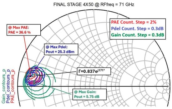
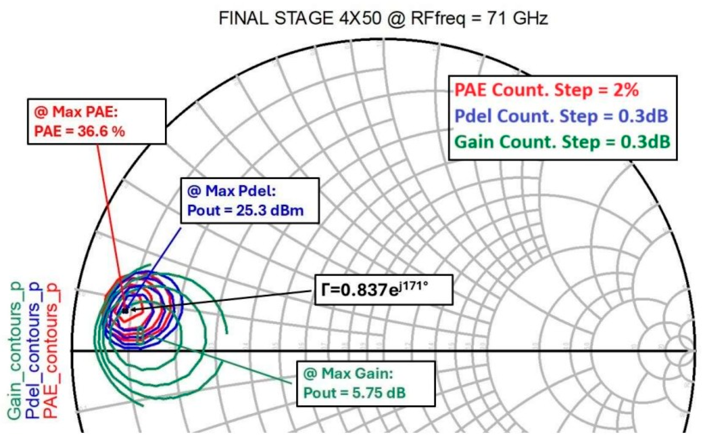
Several simulations were performed to estimate the achievable power performance of suitable device geometries in the bandwidth of interest. Regarding the GaN technology, the drain bias voltage was derated to VDD = 8 V, due to Space Reliability constraints, while the gate bias voltage was kept fixed at −1.25 V, corresponding to class AB operation (ID = 200 mA/mm). Considering the power density of the technology, the required output power can be delivered by a single device in the final stage of the HPA, without the need for any power-combining structure. The most suitable device for this purpose was identified as the 4 × 50 µm transistor. For the selected bias point, a load pull at a fundamental frequency was performed at 71 GHz, assuming a back-side temperature of 80 °C in the simulation and thus obtaining the contour plots reported in Figure 1.
Figure 1.
Load pull of the 4 × 50 µm GaN device, for the bias condition , .
The contour plots of the output power (blue), efficiency (red), and gain (green) are reported in Figure 1. Such performance was achieved at a 1 dB compression level. In order to guarantee the minimum power level of 25 dBm, the optimum load was fixed in the center of the power contour, i.e., ΓL = 0.837ej171°.
After an extensive linear and non-linear simulation campaign on the available device peripheries, it was determined that achieving an overall gain exceeding 20 dB requires a five-stage HPA architecture. The last two stages should be implemented using the 4 × 50 µm device, whereas the first three stages should rely on the 2 × 50 µm device.
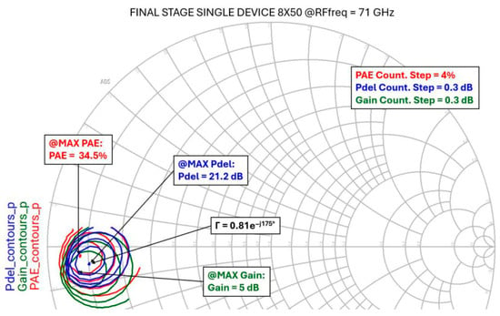
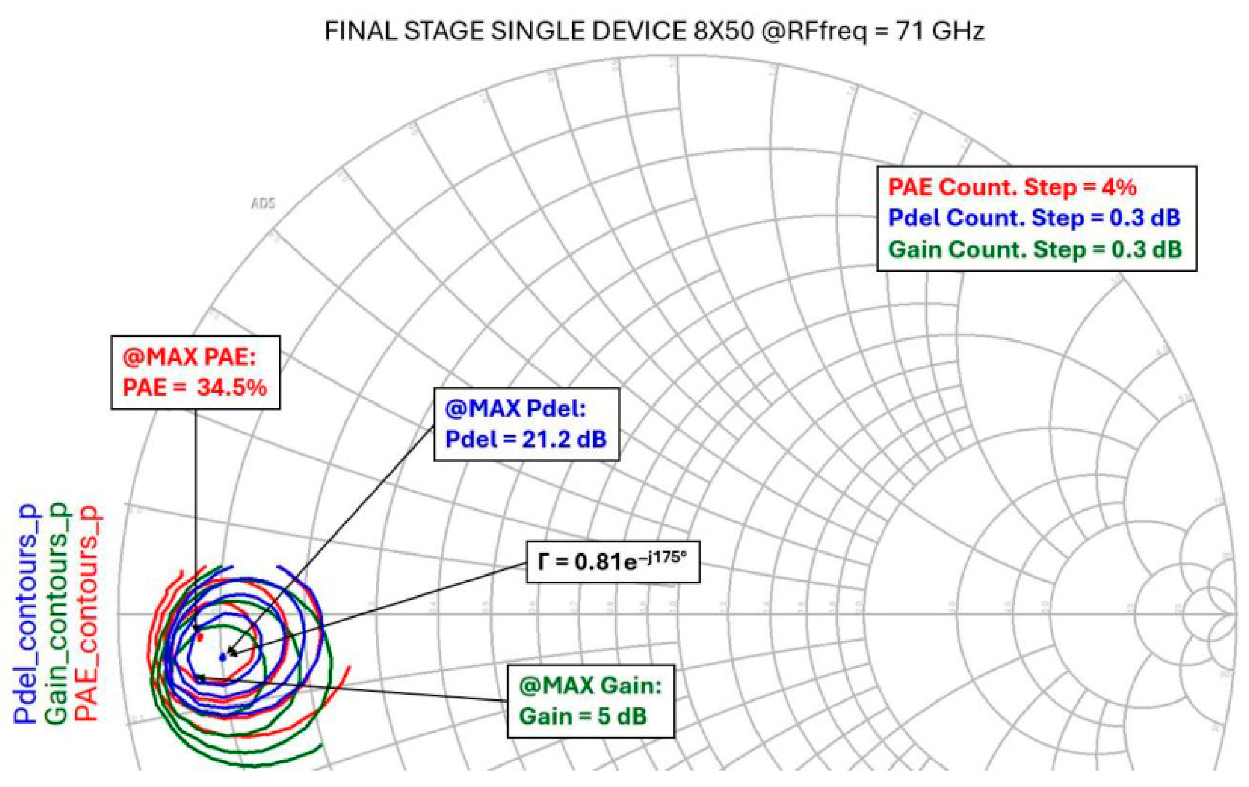
In contrast, for the GaAs technology, the drain bias voltage was derated to VDD = 3 V from the nominal 4 V, while the gate bias voltage was fixed at −0.125 V, corresponding to class AB operation (ID = 110 mA/mm). Unlike the MESC GaN technology, in this case, a single device cannot deliver the required 25.5 dBm output power at the HPA output, making it necessary to combine several elementary devices in the final stage. After an extensive simulation campaign on the available device peripheries, a five-stage architecture was also identified as the most suitable to achieve an overall gain greater than 20 dB. Assuming typical matching-network topologies, it was possible to estimate the device periphery required for each stage and to obtain a reasonable prediction of the overall performance, including efficiency. For the 8 × 50 µm device, a fundamental load-pull analysis was carried out at 71 GHz under the selected bias conditions, assuming a back-side temperature of 80 °C. The resulting contour plot is reported in Figure 2.
Figure 2.
Load pull of the 8 × 50 µm GaAs device, for the bias condition , .
In Figure 2, the contour plots of the output power (blue), PAE (red), and gain (green) are reported. Four parallel devices are necessary to fulfill the specification of 23 dB of saturated power.
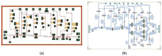
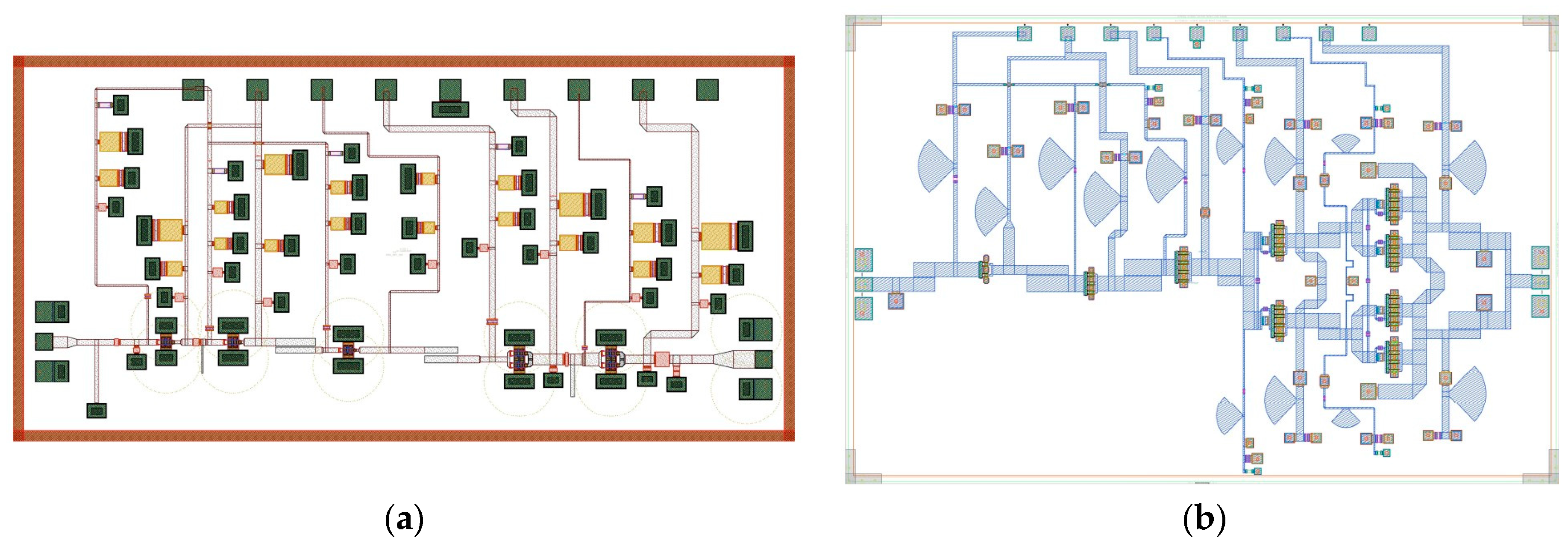
The resulting HPA architecture employs a 4 × 20 µm device in the first stage, a 6 × 30 µm device in the second stage, an 8 × 50 µm device in the third stage, two 8 × 50 µm devices in the fourth stage, and a combination of four 8 × 50 µm devices in the final stage. The HPA layouts of the MMIC for both the GaN and GaAs technologies are shown in Figure 3.
Figure 3.
(a) GaN HPA layout. (b) GaAs HPA layout.
2.2. LNA Design
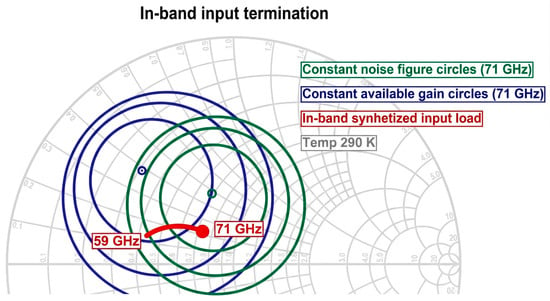
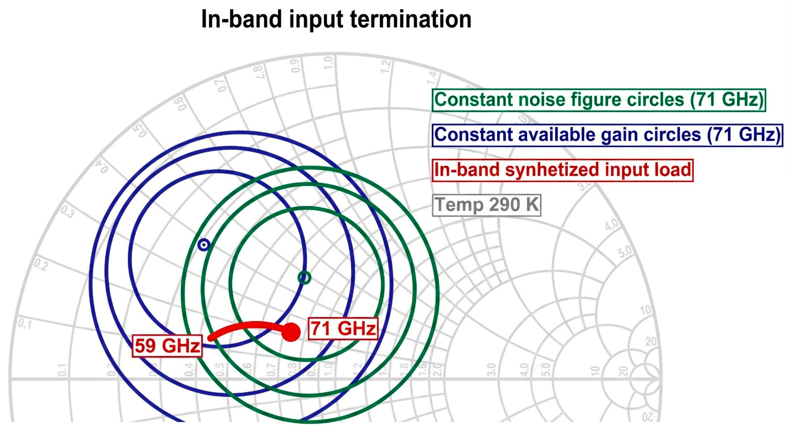
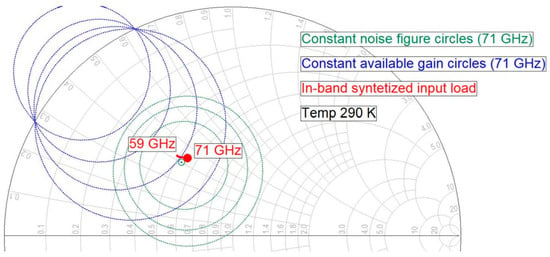
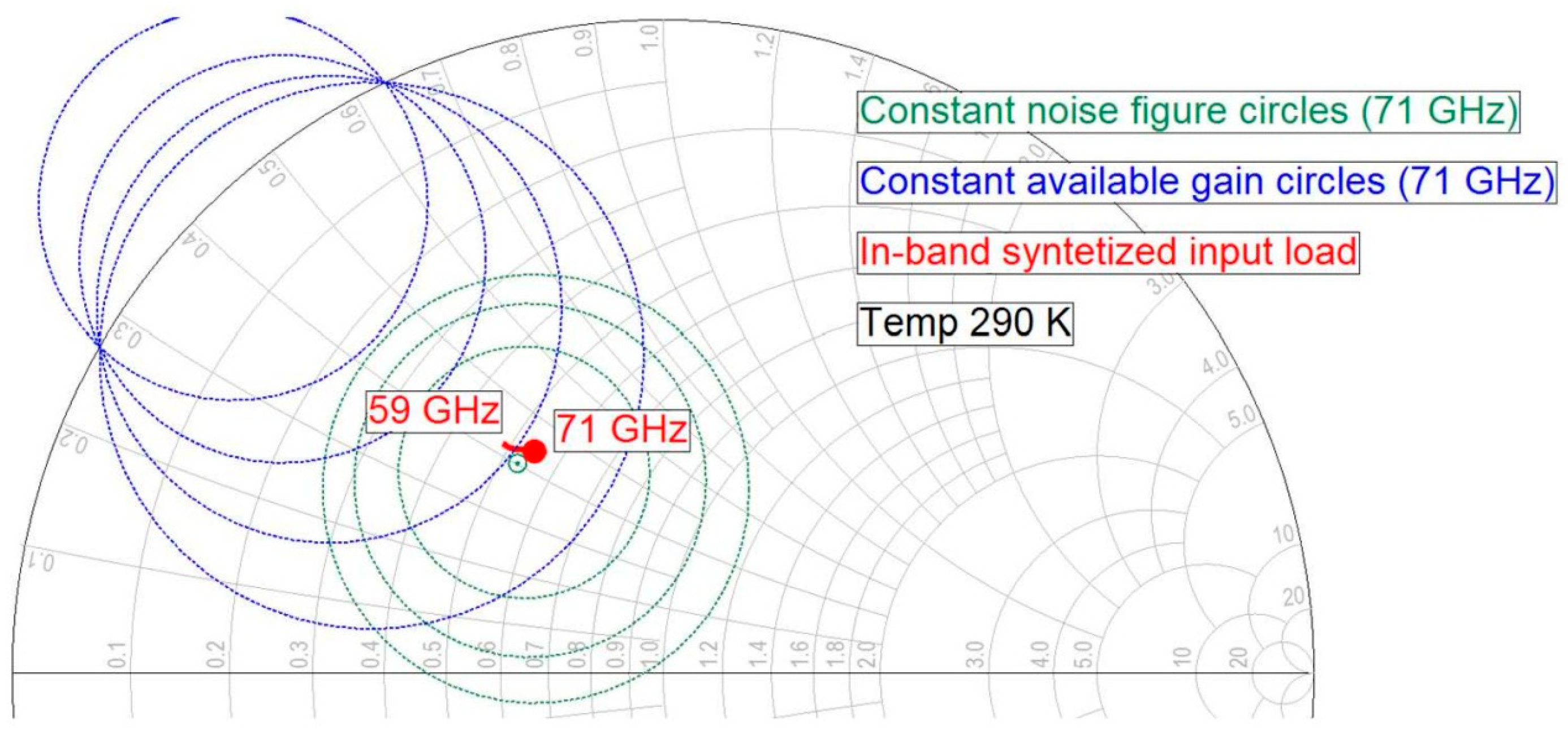
For both the GaN and GaAs LNAs, a preliminary analysis of the optimum device size and bias point for low-noise operation was carried out by evaluating the Minimum Noise Measure (Mmin) for several gate peripheries. In both technologies, the drain-to-source voltage was set to the lowest value for which the model is validated by measurements. In the GaN technology, the gate-to-source voltage corresponding to low-noise operation is approximately equal to 23 % of the device’s maximum current. Under these conditions, the optimum behavior is achieved with a device featuring a Unit Gate Width (UGW) of 20 μm. The number of fingers shows only a mild influence on the Noise Measure performance; therefore, a 2-finger device was selected, as larger devices introduce significant parasitic effects that reduce practical usefulness at V-band, especially in terms of the position of the optimum terminations (Γopt). The synthesized input load for the first stage is depicted in Figure 4 compared to the position of the constant available gain circles and constant noise figure circles.
Figure 4.
Synthesized input termination for first stage (GaN technology).
This load is synthesized with a preference to fit the optimum load in the upper portion of the design band, where the optimal trade-off between gain and noise is most relevant.
Based on the available gain, the minimum 20 dB overall gain requirement can be satisfied with a four-stage architecture [7].
For the GaAs technology, the gate-to-source voltage corresponding to low-noise operation is approximately equal to 12 % of the maximum current. In this case, the optimum behavior is obtained with a device with a Unit Gate Width of 30 μm. Similarly to the GaN case, the number of fingers only mildly affects the Noise Measure performance, so a 2-finger device was selected, since larger peripheries would result in increased parasitic effects and therefore poorer practical behavior at V-band, particularly in terms of Γopt. In Figure 5, the synthesized input load of the first stage is presented in relation to the constant available gain and constant noise figure circles.
Figure 5.
Synthesized input termination for first stage (GaAs technology).
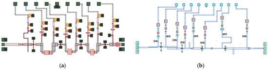
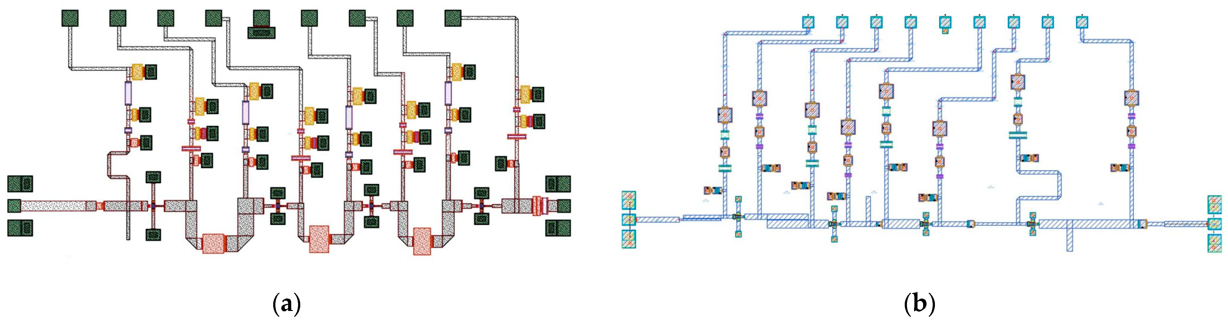
The LNA layouts of the MMIC for both the GaN and GaAs technologies are shown in Figure 6.
Figure 6.
(a) GaN LNA layout. (b) GaAs LNA layout.
2.3. SPDT Design
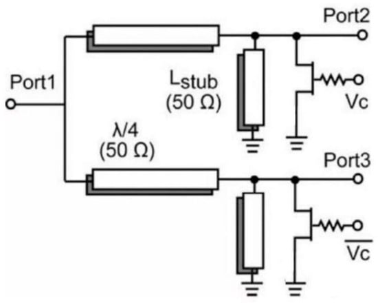
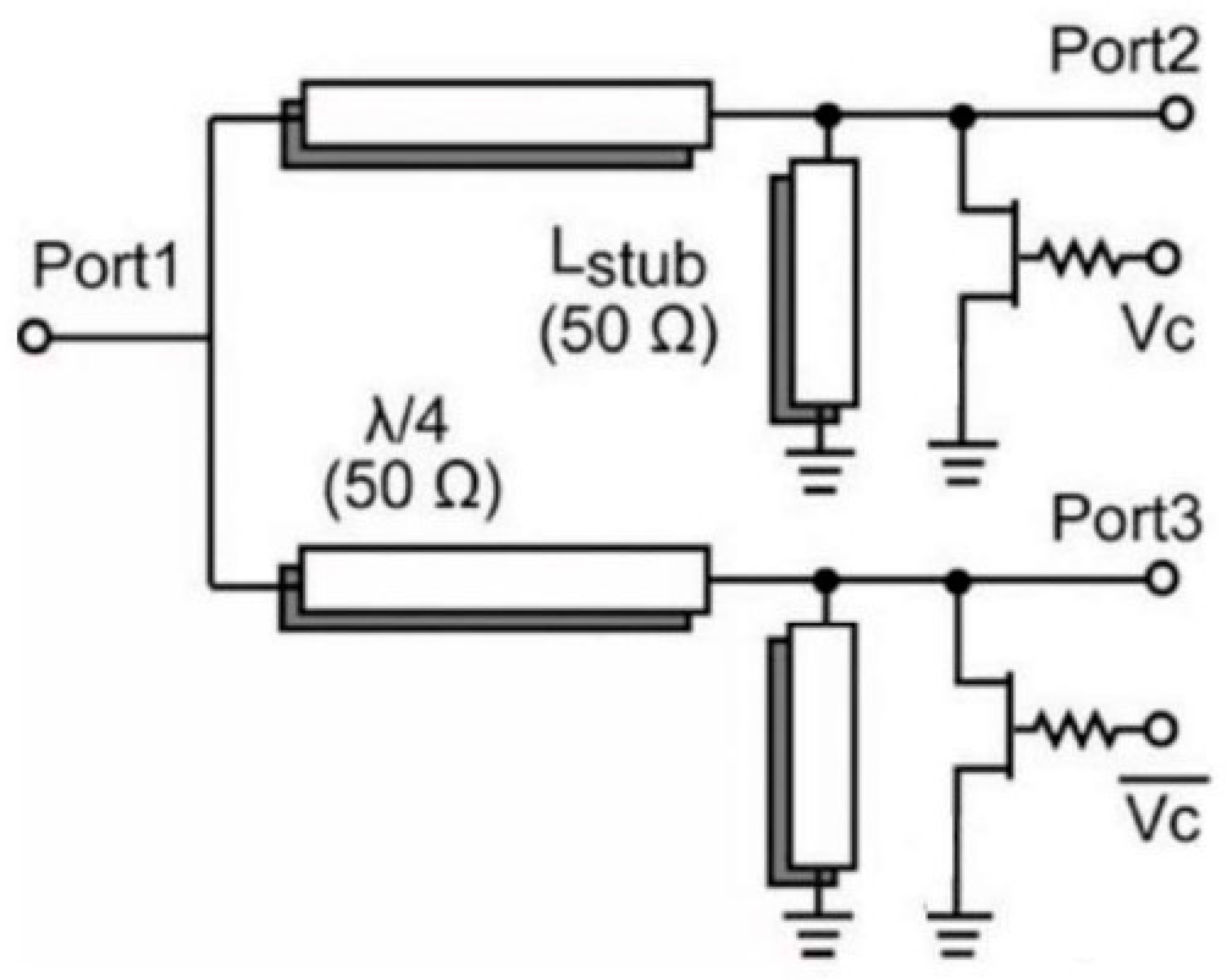
The single-pole double-throw switch adopts a shunt FET configuration in combination with a quarter-wavelength transmission line. A simplified circuit schematic is presented in Figure 7.
Figure 7.
Schematic of an SPDT switch with shunt FET topology.
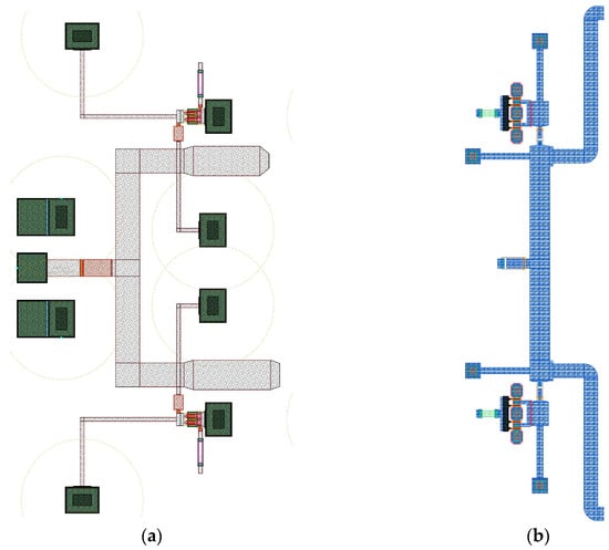
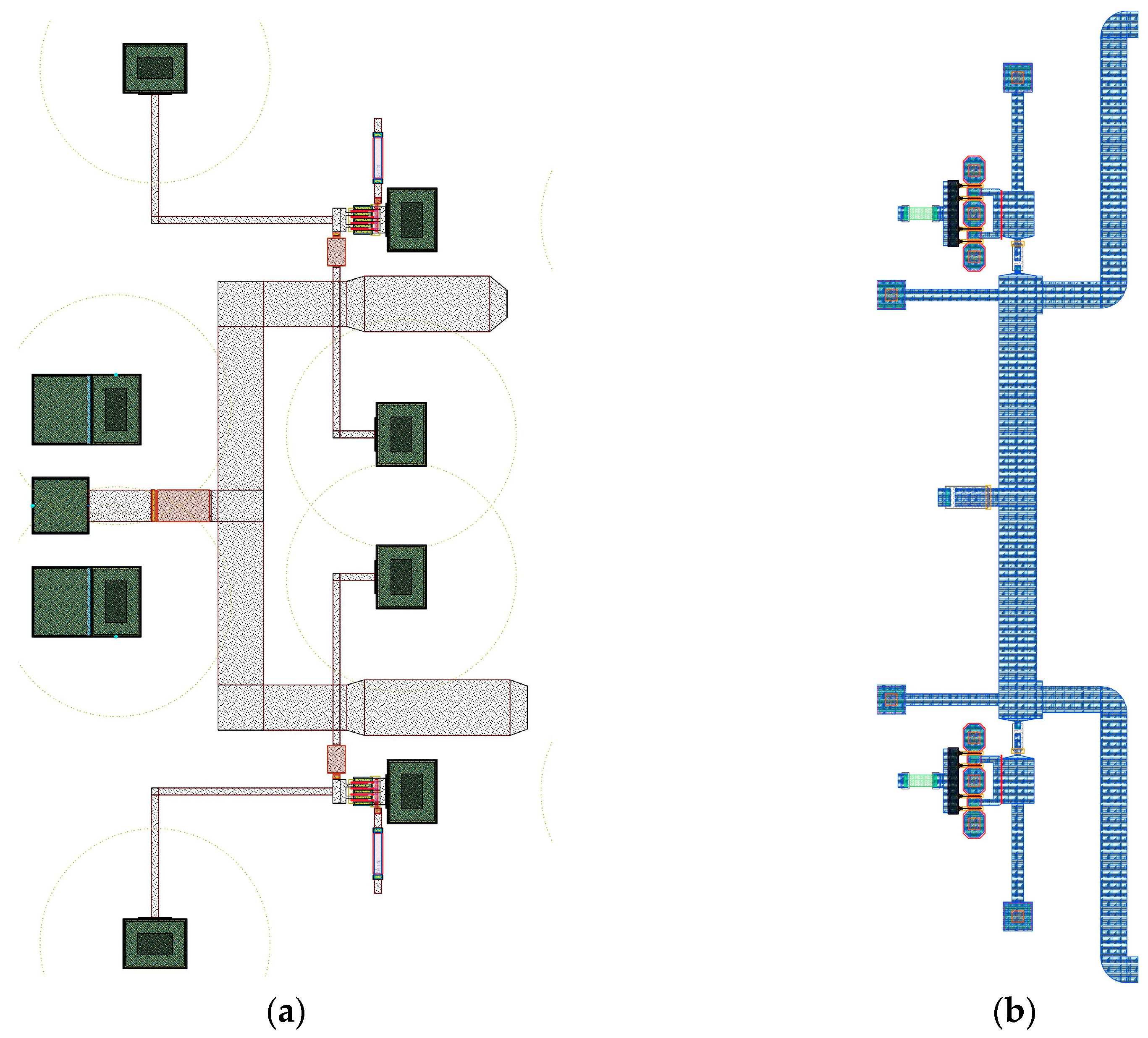
In this topology, the input terminal of the switch is connected to two branches, each incorporating a quarter-wavelength transmission line. At the end of each line, a transistor is placed between the line and ground. When the transistor is in the on-state, it presents low impedance to ground, which is transformed by the λ/4 line into high impedance at the input—effectively isolating that branch. On the opposite branch, the transistor remains in the off-state and is impedance-matched to the transmission line using a parallel stub, implemented with an additional section of transmission line. This shunt stub enhances the isolation of the off-state branch, further improving the switch’s overall performance [15,16]. For the GaN technology, a control voltage of +0 V was selected for the ON state, while −10 V was chosen for the OFF state. For the GaAs technology, the selected control voltages are 0.8 V for the ON state and −6 V for the OFF state. The choice of a positive voltage for the ON state, instead of 0 V, was made to reduce the insertion loss. The SPDT layouts of the MMIC for both the GaN and GaAs technologies are shown in Figure 8.
Figure 8.
(a) GaN SPDT layout. (b) GaAs SPDT layout.
3. Layout and Simulated Performance
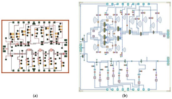
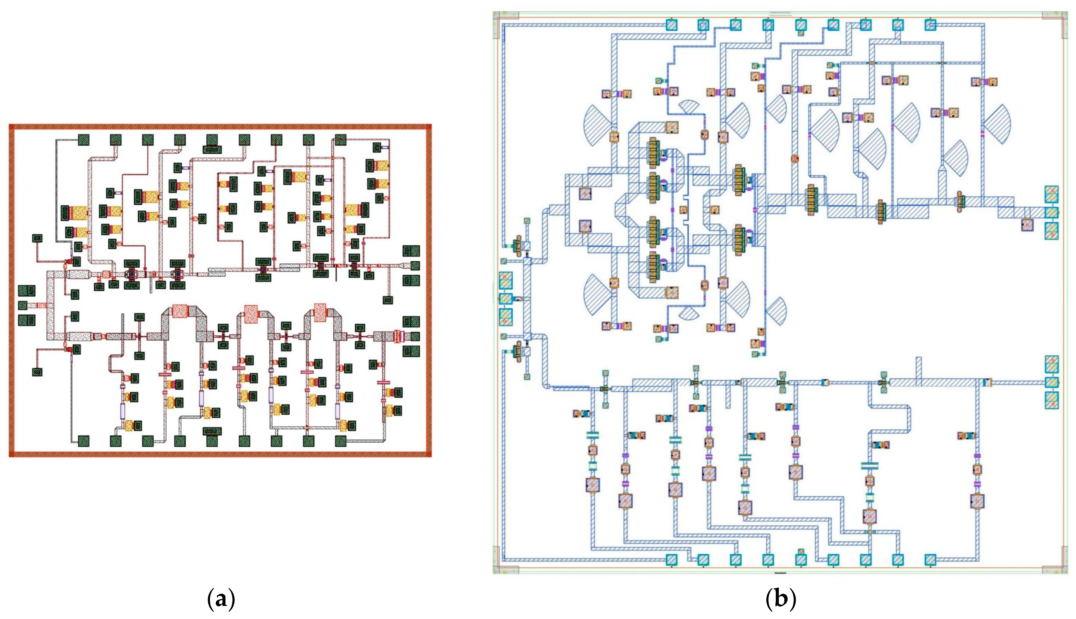
After designing the subsystems as standalone functional blocks, they were subsequently integrated to form the complete MMIC. Figure 9 shows the circuit layout implemented in both technologies. The two circuits are shown to scale to allow a direct visual comparison of the device dimensions. As can be seen, the GaN MMIC occupies nearly half the area of its GaAs counterpart.
Figure 9.
(a) GaN layout. (b) GaAs layout.
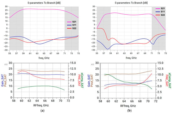
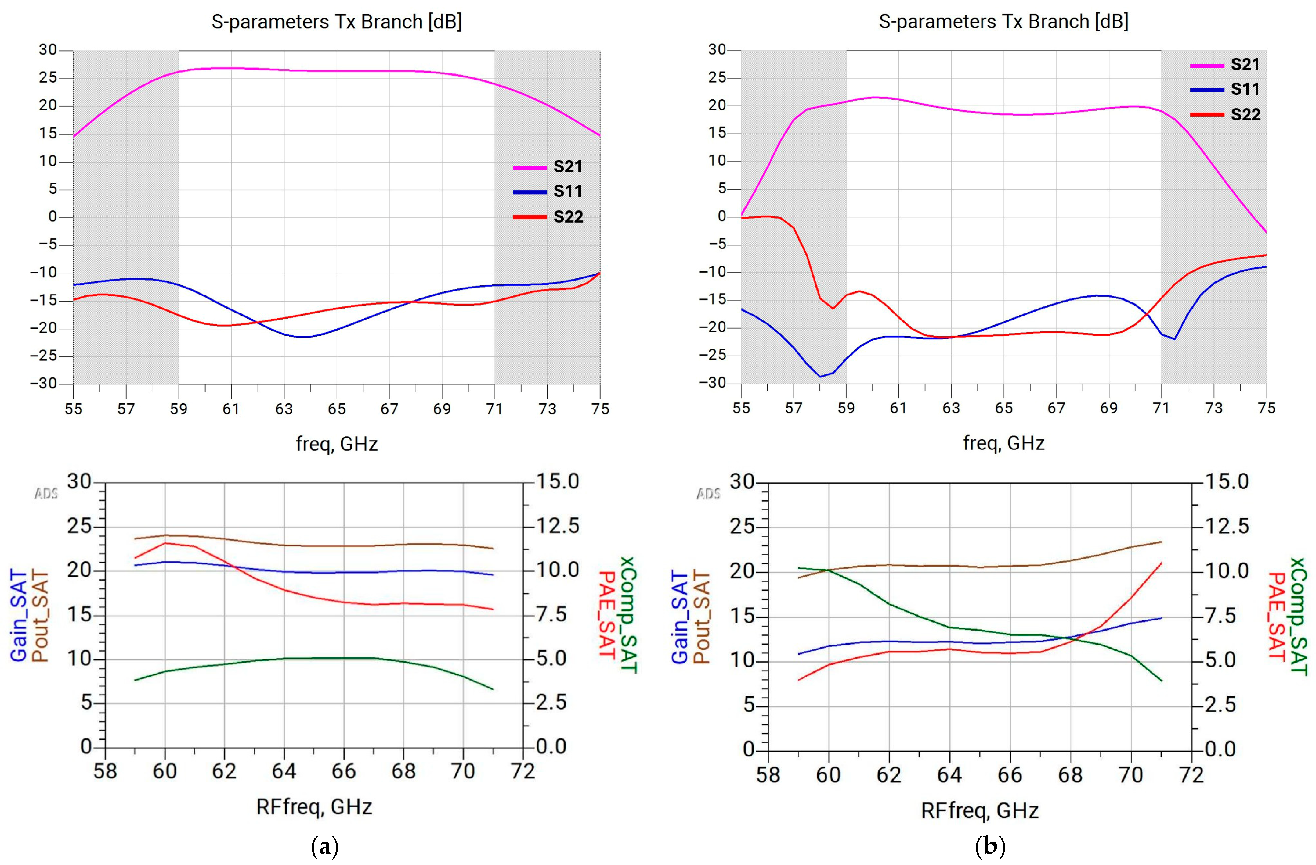
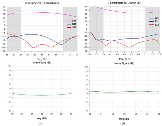
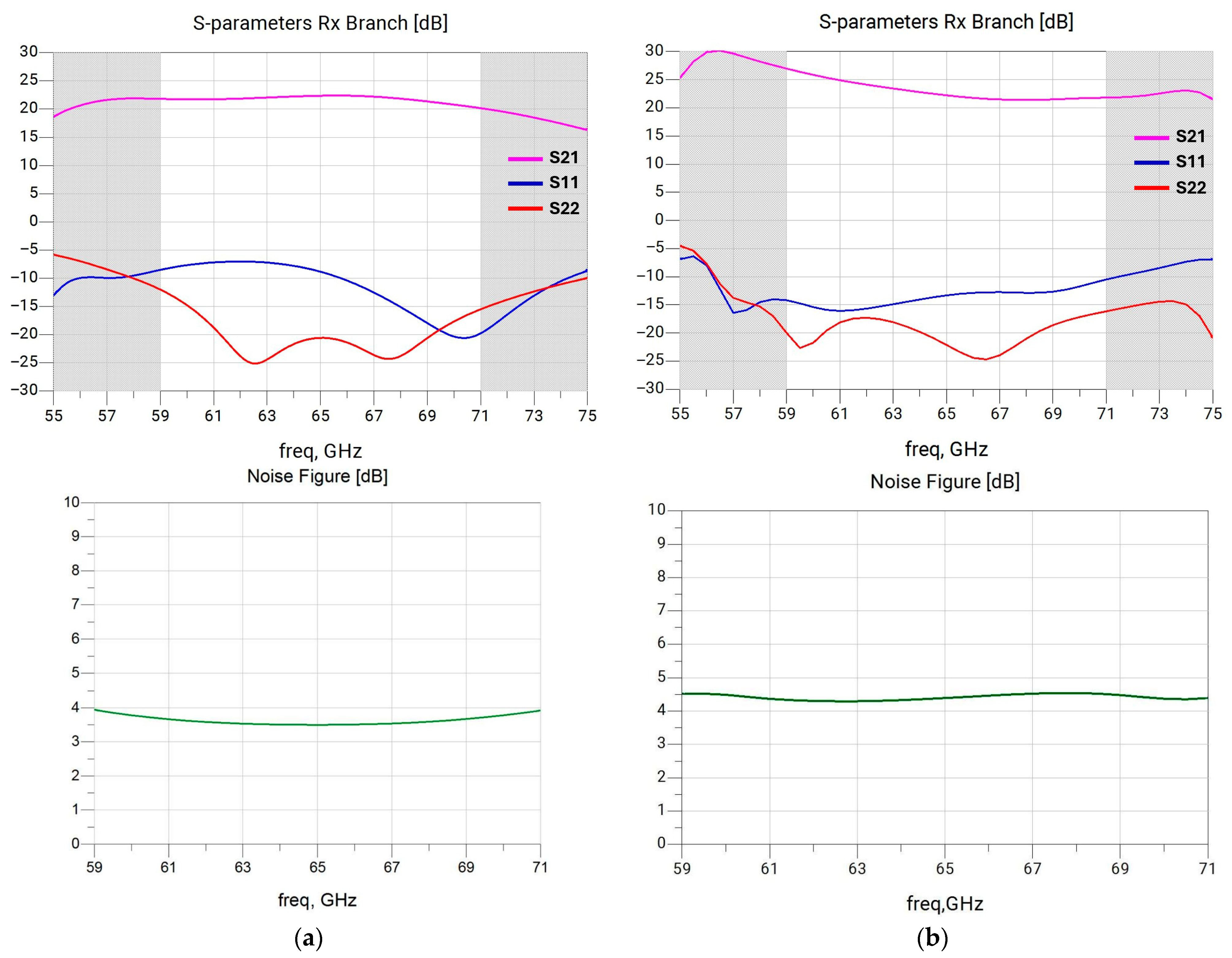
The following figures (Figure 10 and Figure 11) report the linear behavior in Tx mode and Rx mode, expressed in terms of S-parameters focusing on the operating bandwidth 59–71 GHz. The critical performance for Tx and Rx modes are also reported. For RX behavior, this parameter is the noise figure, for Tx, the parameters are output power (Pout) and PAE. The grey shaded area indicates the out-of-band frequency regions.
Figure 10.
(a) GaN Tx performance. (b) GaAs Tx performance.
Figure 11.
(a) GaN Rx performance. (b) GaAs Rx performance.
Analysis of the presented data highlights a clear advantage of the GaN implementation over its GaAs counterpart. The former fully meets the small-signal gain target in both Tx and Rx modes, while the latter satisfies the requirement only in Rx mode, reaching a minimum of 18 dB at center frequency in Tx operation. Moreover, GaN exhibits a lower noise figure, with typical in-band values around 3.7 dB compared to 4.5 dB for GaAs. In Tx mode, the GaN design achieves an average saturated output power of 23 dBm across the band, whereas the GaAs counterpart reaches approximately 21.5 dBm. Additionally, the GaAs T/R chip shows significantly lower non-linear gain, which adversely impacts its power-added efficiency (PAE).
4. Discussion
Many examples of GaN single-chip front-ends (SCFEs) are provided in the literature in bandwidths higher or lower than V-band [17,18]. However, GaN and GaAs contributions at V-band are very rare to find. Table 1 summarize the state of the art and comparatively evaluate this work with the literature, focusing on V-band 50–75 GHz.
Table 1.
State-of-the-art summary of SCFE MMICs, focusing on V-band 50–75 GHz.
5. Conclusions
A V-band single-chip transmit/receive front-end operating over the 59–71 GHz range is presented in this paper. The design methodologies adopted for each MMIC building block—namely, the HPA, LNA and SPDT—were outlined for both technologies, and the final integrated front-end layout, along with its performance, was reported. Simulation results clearly indicate the superior performance of the GaN implementation compared to its GaAs counterpart. The GaN design fully meets the small-signal gain target in both Tx and Rx modes, whereas the GaAs solution satisfies this requirement only in Rx mode, achieving a minimum of 18 dB at center frequency in Tx mode. In addition, the GaN front-end exhibits a lower in-band noise figure, with average values around 3.7 dB compared to 4.5 dB for GaAs. In Tx operation, it delivers an average saturated output power of 23 dBm across the band, while the GaAs design reaches approximately 21.5 dBm. The reduced non-linear gain of the GaAs implementation also results in a lower power-added efficiency. Finally, the GaN solution demonstrates a significantly more compact footprint, with an area of 12.3 mm2 compared to 27.8 mm2 for the GaAs counterpart.
Author Contributions
Conceptualization, G.V., A.R., and M.R.; methodology, all; validation, all; formal analysis, all; investigation, all; resources, E.L.; writing—original draft preparation, G.V.; writing—review and editing, all; visualization, all; supervision, P.E.L. and R.G.; project administration, P.E.L. and R.G.; funding acquisition, E.L. All authors have read and agreed to the published version of the manuscript.
Funding
This research was funded by the European Space Agency, grant number AO/1-11802/23/NL/AF “RF transmit and receive front-end for V-band inter-satellite link”, whose support is gratefully acknowledged. The views expressed in this publication can in no way be taken to reflect the official opinion of the European Space Agency.
Data Availability Statement
No publicly available datasets were generated or analyzed in this study. The data supporting the findings are available from the corresponding author upon reasonable request.
Conflicts of Interest
The authors declare no conflicts of interest.
References
- Kaushal, H.; Kaddoum, G. Optical Communication in Space: Challenges and Mitigation Techniques. IEEE Commun. Surv. Tutor. 2016, 19, 57–96. [Google Scholar] [CrossRef] [Scilit]
- Jiang, W.Y.; Ma, Z.L. A Microwave/Millimeter-Wave Dual-Band Shared-Aperture Antenna for S/V-Bands Applications. In Proceedings of the 2024 IEEE 10th International Symposium on Microwave, Antenna, Propagation and EMC Technologies for Wireless Communications (MAPE), Guangzhou, China, 27–30 November 2024. [Google Scholar] [CrossRef] [Scilit]
- Giordani, R.; Amici, M.; Barigelli, A.; Conti, F.; Del Marro, M.; Feudale, M.; Imparato, M.; Suriani, A. Highly integrated and solderless LTCC based C-band T/R module. In Proceedings of the 2009 European Microwave Conference (EuMC), Rome, Italy, 28–29 September 2009. [Google Scholar] [CrossRef] [Scilit]
- Chou, Y.-T.; Chiong, C.-C.; Wang, H. A Q-band LNA with 55.7% bandwidth for radio astronomy applications in 0.15-μm GaAs pHEMT process. In Proceedings of the 2016 IEEE International Symposium on Radio-Frequency Integration Technology (RFIT), Taipei, Taiwan, 24–26 August 2016. [Google Scholar] [CrossRef] [Scilit]
- Colangeli, S.; Ciccognani, W.; Longhi, P.E.; Pace, L.; Poulain, J.; Leblanc, R.; Limiti, E. Linear Characterization and Modeling of GaN-on-Si HEMT Technologies with 100 nm and 60 nm Gate Lengths. Electronics 2021, 10, 134. [Google Scholar] [CrossRef] [Scilit]
- Florian, C.; Cignani, R.; Niessen, D.; Santarelli, A. A C-Band AlGaN-GaN MMIC HPA for SAR. IEEE Microw. Wirel. Compon. Lett. 2012, 22, 471–473. [Google Scholar] [CrossRef] [Scilit]
- Pace, L.; Ciccognani, W.; Colangeli, S.; Longhi, P.E.; Limiti, E.; Leblanc, R. A Ka-Band Low-Noise Amplifier for Space Applications in a 100 nm GaN on Si technology. In Proceedings of the 2019 15th Conference on Ph.D Research in Microelectronics and Electronics (PRIME), Lausanne, Switzerland, 15–18 July 2019. [Google Scholar] [CrossRef] [Scilit]
- Setiawan, A.; Maulana, Y.Y.; Sulaeman, Y.; Praludi, T.; Taryana, Y. Design of 3 GHz stripline ferrite circulator for radar applications. In Proceedings of the 2017 International Conference on Radar, Antenna, Microwave, Electronics, and Telecommunications (ICRAMET), Jakarta, Indonesia, 23–24 October 2017. [Google Scholar] [CrossRef] [Scilit]
- Ciccognani, W.; Colangeli, S.; Costanzo, F.; Giofre, R.; Polli, G.; Salvucci, A.; Vittori, M.; Limiti, E.; Sotgia, M.; Cirillo, M. A GaN Single-Chip Front-End for Active Electronically Scanned Arrays. In Proceedings of the 2018 IEEE/MTT-S International Microwave Symposium-IMS, Philadelphia, PA, USA, 10–15 June 2018. [Google Scholar] [CrossRef] [Scilit]
- Sharma, S.S.; Longhi, P.E.; Colangeli, S.; Ciccognani, W.; Limiti, E. A C-Band MMIC Multi-Functional Core Chip with 7 Bits Phase Shifter and Attenuator Using GaAs pHEMT. In Proceedings of the 2024 19th Conference on PhD Research in Microelectronics and Electronics (PRIME), Larnaca, Cyprus, 9–12 June 2024. [Google Scholar] [CrossRef] [Scilit]
- van Heijningen, M.; de Hek, P.; Dourlens, C.; Fellon, P.; Adamiuk, G.; Ayllon, N.; van Vliet, F. C-Band Single-Chip Radar Front-End in AlGaN/GaN Technology. IEEE Trans. Microw. Theory Tech. 2017, 65, 4428–4437. [Google Scholar] [CrossRef] [Scilit]
- Bentini, A.; Ferrari, M.; Ciccognani, W.; Limiti, E. A novel approach to minimize RMS errors in multifunctional chips. Int. J. RF Microw. Comput. Eng. 2012, 22, 387–393. [Google Scholar] [CrossRef] [Scilit]
- Limiti, E.; Ciccognani, W.; Cipriani, E.; Colangeli, S.; Colantonio, P.; Palomba, M.; Florian, C.; Pirola, M.; Ayllon, N. T/R modules front-end integration in GaN technology. In Proceedings of the 2015 IEEE 16th Annual Wireless and Microwave Technology Conference (WAMICON), Cocoa Beach, FL, USA, 13–15 April 2015. [Google Scholar] [CrossRef] [Scilit]
- Choi, P.; Goswami, S.; Radhakrishna, U.; Khanna, D.; Boon, C.-C.; Lee, H.-S.; Antoniadis, D.; Peh, L.-S. A 5.9-GHz Fully Integrated GaN Frontend Design With Physics-Based RF Compact Model. IEEE Radio Freq. Integr. Circuits Symp. 2015, 63, 1163–1173. [Google Scholar] [CrossRef] [Scilit]
- Thome, F.; Ambacher, O. Highly Isolating and Broadband Single-Pole Double-Throw Switches for Millimeter-Wave Applications Up to 330 GHz. IEEE Trans. Microw. Theory Tech. 2017, 66, 1998–2009. [Google Scholar] [CrossRef] [Scilit]
- Thome, F.; Bruckner, P.; Quay, R.; Ambacher, O. Millimeter-Wave Single-Pole Double-Throw Switches Based on a 100-nm Gate-Length AlGaN/GaN-HEMT Technology. In Proceedings of the 2019 IEEE/MTT-S International Microwave Symposium-IMS, Boston, MA, USA, 2–7 June 2019. [Google Scholar] [CrossRef] [Scilit]
- Sonnenberg, T.; Romano, A.; Miller, N.C.; Popović, Z. A W-Band GaN MMIC Single-Chip T/R Front End. IEEE Trans. Microw. Theory Tech. 2024, 72, 5830–5837. [Google Scholar] [CrossRef] [Scilit]
- Longhi, P.E.; Pace, L.; Costanzo, F.; Ciccognani, W.; Colangeli, S.; Giofrè, R.; Leblanc, R.; Suriani, A.; Vitobello, F.; Limiti, E. 32–36-GHz Single-Chip Front-End MMIC Featuring 35-dBm Output Power and 3.2-dB Noise Figure With 60- and 100-nm GaN/Si HEMTs. IEEE Trans. Microw. Theory Tech. 2023, 72, 160–172. [Google Scholar] [CrossRef] [Scilit]
- Gadallah, A.; Eissa, M.H.; Kissinger, D.; Malignaggi, A. Performance Comparison of V-band T/R Amplifier Module in SiGe Technology using Aluminium and Copper Back-end of line. In Proceedings of the 2022 IEEE 22nd Topical Meeting on Silicon Monolithic Integrated Circuits in RF Systems (SiRF), Las Vegas, NV, USA, 16–19 January 2022. [Google Scholar] [CrossRef] [Scilit]
- Gadallah, A.; Eissa, M.H.; Kissinger, D.; Malignaggi, A. A V-Band Miniaturized Bidirectional Switchless PALNA in SiGe:C BiCMOS Technology. IEEE Microw. Wirel. Compon. Lett. 2020, 30, 786–789. [Google Scholar] [CrossRef] [Scilit]
- Meng, F.; Ma, K.; Yeo, K.S.; Boon, C.C.; Yi, X.; Sun, J.; Feng, G.; Xu, S. A Compact 57–67 GHz Bidirectional LNAPA in 65-nm CMOS Technology. IEEE Microw. Wirel. Compon. Lett. 2016, 26, 628–630. [Google Scholar] [CrossRef] [Scilit]

Disclaimer/Publisher’s Note: The statements, opinions and data contained in all publications are solely those of the individual author(s) and contributor(s) and not of MDPI and/or the editor(s). MDPI and/or the editor(s) disclaim responsibility for any injury to people or property resulting from any ideas, methods, instructions or products referred to in the content. |
© 2026 by the authors. Licensee MDPI, Basel, Switzerland. This article is an open access article distributed under the terms and conditions of the Creative Commons Attribution (CC BY) license.