


Abstract
The efficiency of wireless systems critically depends on the ability of antennas to transfer power from the transmitter circuitry into free space. Although maximum power transfer is theoretically achieved under perfect impedance matching, IoT devices rarely meet this condition due to the ever-changing conditions of the surrounding environment. As a result, a portion of the transmitted power is reflected, reducing the effectively radiated power and degrading system performance. In addition to these radiated losses, load mismatch at the power amplifier output can lead to gain degradation, increased power dissipation, and impaired performance of linearization schemes such as digital predistortion. Such an effect is well-known but has never been quantified. The purpose of this paper is to quantify not only the losses arising from reflection due to impedance mismatch but also those associated with the reduction in amplifier gain by considering both antenna- and amplifier-level perspectives. Theoretical calculations of mismatch losses are first developed and analysed. These results are subsequently validated in an idealised environment, followed by experimental demonstrations in realistic device scenarios, where substantial discrepancies with theoretical predictions and controlled measurements are observed. The findings quantitatively separate and superimpose, for the first time in a unified experimental framework, the radiative mismatch losses (antenna and matching network) from the additional power amplifier gain degradation under realistic load conditions. This demonstrates that passive antenna measurements alone significantly underestimate the total radiated power loss in practical IoT devices. The results emphasise the need to account for real-world operating conditions when evaluating mismatch-induced losses and highlight the importance of co-design and adaptive strategies for both antennas and power amplifiers in future wireless and IoT systems.
1. Introduction
The rapid growth of wireless communications, driven by the increasing penetration of Internet of Things (IoT) devices and the deployment of emerging 5G and 6G networks, has placed unprecedented emphasis on the efficient use of radiated power, which directly impacts power consumption and communication range. This issue is particularly critical in the IoT domain, where devices are often battery-powered, operate under severe energy constraints, and are expected to function reliably over long periods without maintenance [1]. Any loss in radiated power not only reduces communication range but also forces devices to compensate for it by transmitting at higher power levels, accelerating battery depletion. Furthermore, in dense IoT deployments, inefficient radiation can lead to unnecessary interference and degraded spectrum utilisation [2]. These challenges highlight the importance of thoroughly investigating the role of antenna impedance mismatch in practical scenarios.
In this context, antennas constitute a fundamental component, as they provide the interface between the electronic circuitry of a device and the propagation medium. The efficiency with which an antenna transfers power from the transmitter to free space is a determining factor in system performance, influencing link reliability, coverage, and energy consumption [3].
Under ideal conditions, it is well known that maximum power transfer is achieved when the antenna impedance perfectly matches (conjugate matching) that of the transmitter circuitry [3]. Variations in user interaction and surrounding materials lead to antenna impedance mismatch, which in turn causes part of the transmitted power to be reflected toward the source instead of being radiated into space [4]. This mismatch is typically quantified through parameters such as the reflection coefficient (, also referred to as S11. Although S11 provides valuable information, it does not fully capture the actual reduction in radiated power caused by antenna impedance mismatches under realistic operating conditions [5].
There are limitations regarding antenna efficiency and impedance behaviour in wireless devices, where practical constraints are often not considered, such as limited space, critical cost, and additional components like sensors or batteries that strongly influence antenna performance [6,7]. Consequently, there remains a gap in the understanding of how antenna impedance mismatch directly affects the power radiated into space in IoT devices, considering the real behaviour of transceivers and not the ideal 50 Ω radiofrequency sources connected to the antenna.
In addition to the mismatch losses at the antenna–transmitter interface, another critical factor often overlooked in practical device performance is the loss of amplifier gain when the amplifier experiences load impedance mismatch [8]. Power amplifiers are designed to deliver maximum gain, efficiency, and linearity under certain load conditions [9]; when the load impedance deviates from the design value, several deleterious effects occur. First, the mismatch generates reflections back toward the amplifier output, altering the amplifier’s output network load and thus shifting its operating point [10]. This shift can reduce available gain because the amplifier no longer operates under the intended load-line, and reactive mismatches can introduce phase shifts and reduce gain at specific frequencies [11]. Second, mismatch-induced reflected power can lead to increased power dissipation within the amplifier, forcing it to operate under thermal stress. Elevated temperature degrades transistor parameters and further reduces gain, while thermal drift exacerbated by mismatch may also increase nonlinear distortion [11]. Third, for amplifiers employing Digital Predistortion (DPD) or other linearization techniques, load mismatch not only reduces raw gain but also impairs the ability of these schemes to correct distortions [12]. Since adaptive predistortion assumes a relatively stable load, dynamic mismatch caused by environmental changes or user interaction significantly worsens its performance [13,14].
In summary, it is well-known that impedance mismatch not only affects the fraction of power radiated through the antenna but also contributes to the amplifier gain degradation in the transmitter. For wireless devices, these conditions occur in dynamic environments. For example, a tracking device may be located on top of a wooden pallet, but could also be changed to a metallic container. Each scenario impacts the device, producing an impedance mismatch. These loss mechanisms are essential to fully understand how much radiated power in IoT devices is lost, and to develop mitigation strategies such as adaptive impedance tuning, reconfigurable antenna systems, and robust PA/DPD design [15,16,17]. However, this effect has not been quantitatively analysed in prior works. Therefore, the purpose of this paper is to quantify both radiated power loss mechanisms—radiative mismatch loss and PA gain loss—under impedance mismatch conditions.
To the best of the authors’ knowledge, although antenna mismatch and PA load sensitivity have been studied separately, no previous work has quantitatively separated and combined both effects within the same unified experimental framework using identical antenna prototypes. The present study fills this gap by comparing simulations, passive measurements, and active measurements with a real low-power transceiver on the same four PCB configurations, thereby isolating the additional losses caused by a power amplifier gain degradation under realistic IoT conditions.
The remainder of this paper is structured as follows. Section 2 presents the theoretical framework and analytical derivations concerning the antenna impedance mismatch, establishing the foundations for subsequent analysis. Section 3 validates these theoretical results under controlled, ideal conditions, thereby isolating the fundamental effects of mismatch from a transceiver. Section 4 extends the investigation to realistic IoT environments, demonstrating that theoretical predictions and ideal results diverge significantly when practical constraints are introduced. Finally, Section 5 discusses the implications of these findings for the design of efficient wireless systems and outlines potential directions for mitigating mismatch effects when designing efficient wireless devices.
2. Theoretical Analysis of Antenna Mismatch
To ensure consistent terminology is used throughout the paper, the following definitions are adopted, based on standard IEEE antenna terminology and the antenna booster framework [5]:
- Radiation Efficiency (): Ratio of the power radiated by the antenna to the power accepted (delivered) at the antenna port. It accounts only for ohmic (conductor) and dielectric losses within the radiating structure and ground plane; it does not include mismatch losses.
- Mismatch Efficiency (): Fraction of the incident power that is accepted by the antenna, where is the input reflection coefficient referenced to the source impedance (typically 50 Ω).
- Matching Network Efficiency (): Accounts for the ohmic losses in the lumped-element matching network. This efficiency degrades when the antenna presents a very low resistance (high current), as occurs under severe mismatch.
- Total Efficiency (): Overall ratio of the Total Radiated Power (TRP) to the power delivered by the source (or transceiver). It includes all loss mechanisms: radiation efficiency, mismatch efficiency, and matching network losses. Mathematically, this can be expressed as .
In this work, the term total efficiency is used when referring to the measured or simulated end-to-end radiated performance (TRP/Pin), while radiation efficiency refers exclusively to the intrinsic efficiency of the radiating structure (excluding mismatch and matching-network losses).
The efficiency of an antenna is governed by the degree of impedance matching between the radiating element and the transmitter circuitry [18]. Maximum power transfer occurs when the antenna input impedance, , is equal to the complex conjugate of the source impedance, . Any deviation from this condition introduces a reflection coefficient, , given by:
where represents the fraction of power reflected toward the source. In microwave engineering, this reflection is conventionally expressed through the parameter . The proportion of accepted power at the antenna port is thus . Consequently, the TRP under mismatch conditions can be expressed as (2):
where is the input power delivered to the antenna port, is the radiation efficiency of the antenna in the absence of a mismatch, represents the efficiency of the matching network, accounts for mismatch loss, and is total efficiency, which includes all loss mechanisms (antenna and mismatch) [5].
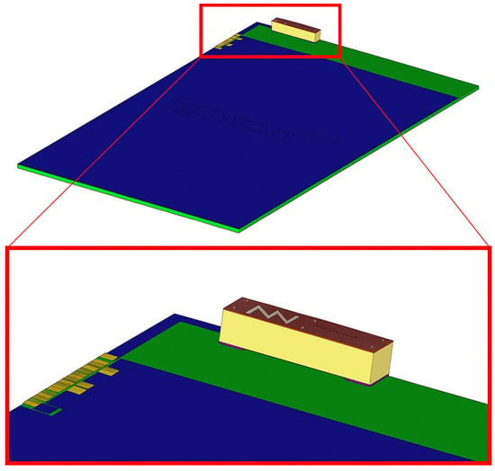
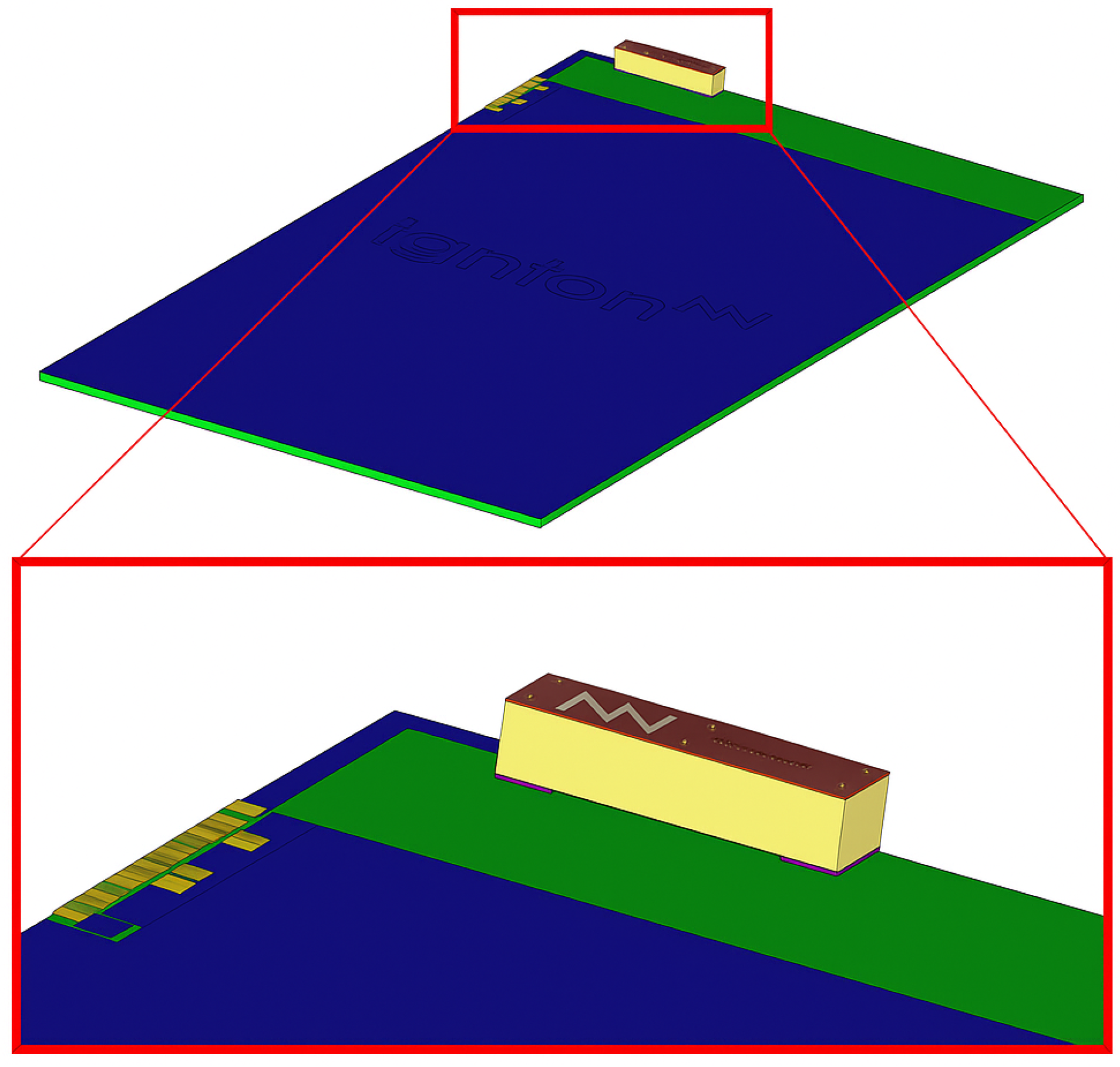
To illustrate the impact of mismatch under controlled conditions, four representative Printed Circuit Board (PCB) designs were modelled and simulated, embedding an antenna booster (Figure 1). It should be noted that the current analysis applies to any antenna technology, particularly those connected to an amplifier and no SWR protection, as in IoT wireless devices. Each configuration employed the same antenna element integrated with a matching network, thereby isolating the effect of mismatch. Hence, the antenna element is an antenna booster (Figure 1): an electrically small non-resonant element that, with the addition of a matching network, can operate at the desired frequency of operation [5]. This simplifies the analysis, since it is easy to modify the antenna impedance system, not by modifying the antenna, which may change the radiation efficiency , but only the matching network, preserving the same .
Figure 1.
3D view of the PCB showing the antenna booster and matching network feed line.
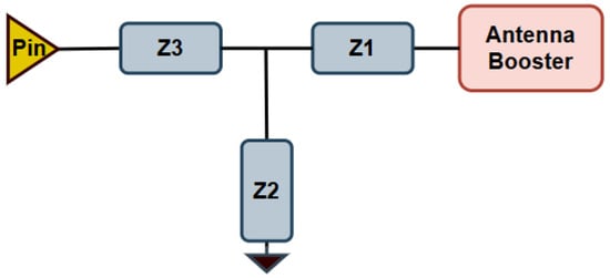
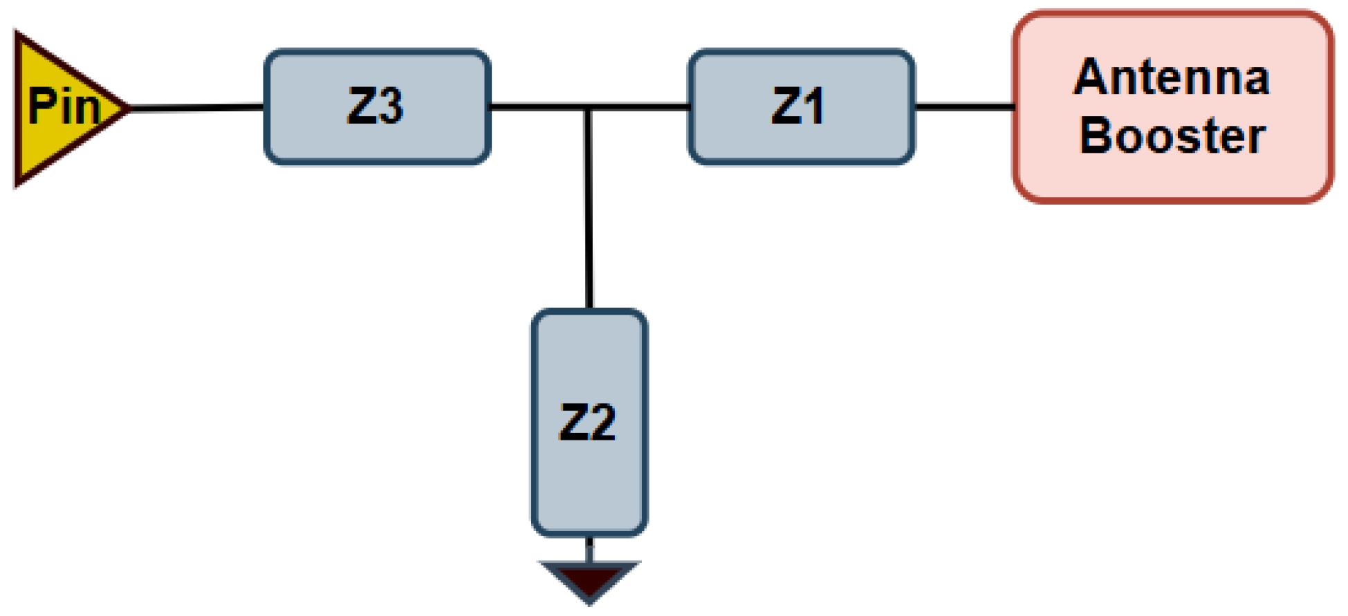
Regarding the four PCB configurations, they aim to systematically represent a progressive degradation of impedance matching conditions, ranging from near-perfect (~−20 dB) to severe mismatch (~−1 dB). This approach enables a clear observation of the relationship between the parameter and TRP over the same frequency band. PCB#1 serves as the reference case, with optimal impedance matching, representative of a well-designed commercial system. PCB#2 introduces a moderate mismatch to emulate a typical deviation due to manufacturing tolerances. PCB#3 and PCB#4 intentionally incorporate pronounced and extreme mismatches, respectively, to reproduce the conditions that might occur in practical scenarios, such as user proximity or nearby conductive elements (e.g., the wireless devices on top of a conductive body). This graded selection allows for the impact of mismatch severity on radiated efficiency to be quantified in a controlled and comparable manner. The four PCB configurations are detailed below, highlighting their respective impedance matching characteristics and expected efficiency performance. The schematic and component values of these networks are summarised in Figure 2 and Table 1, and are consistently used for simulation, PCB fabrication, and the experimental evaluations presented in Section 3 and Section 4.
Figure 2.
Matching network topologies implemented in the four PCB configurations evaluated in this work.
Table 1.
Matching network configurations.
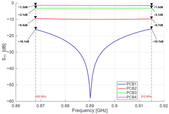
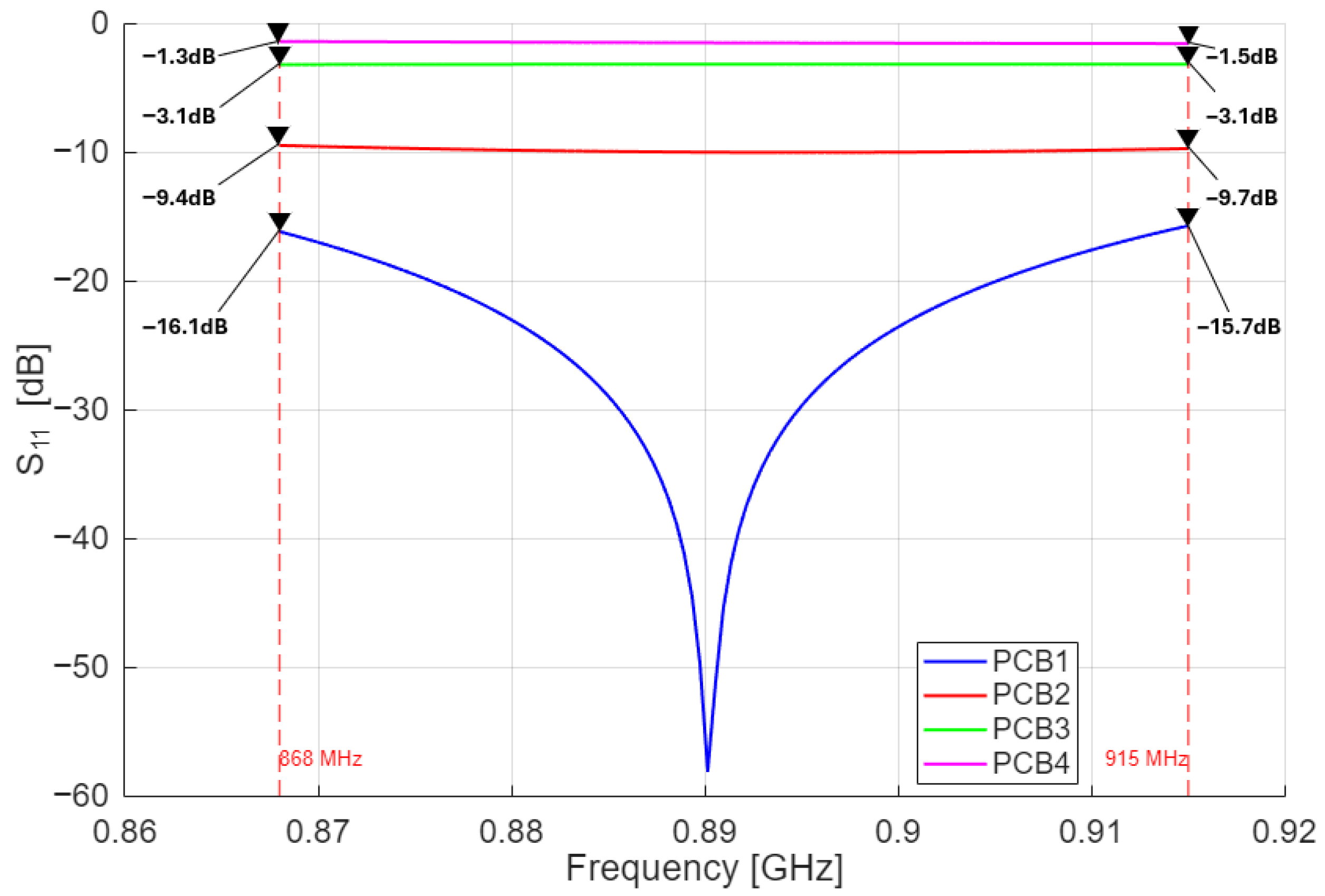
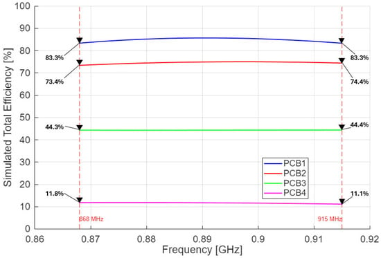
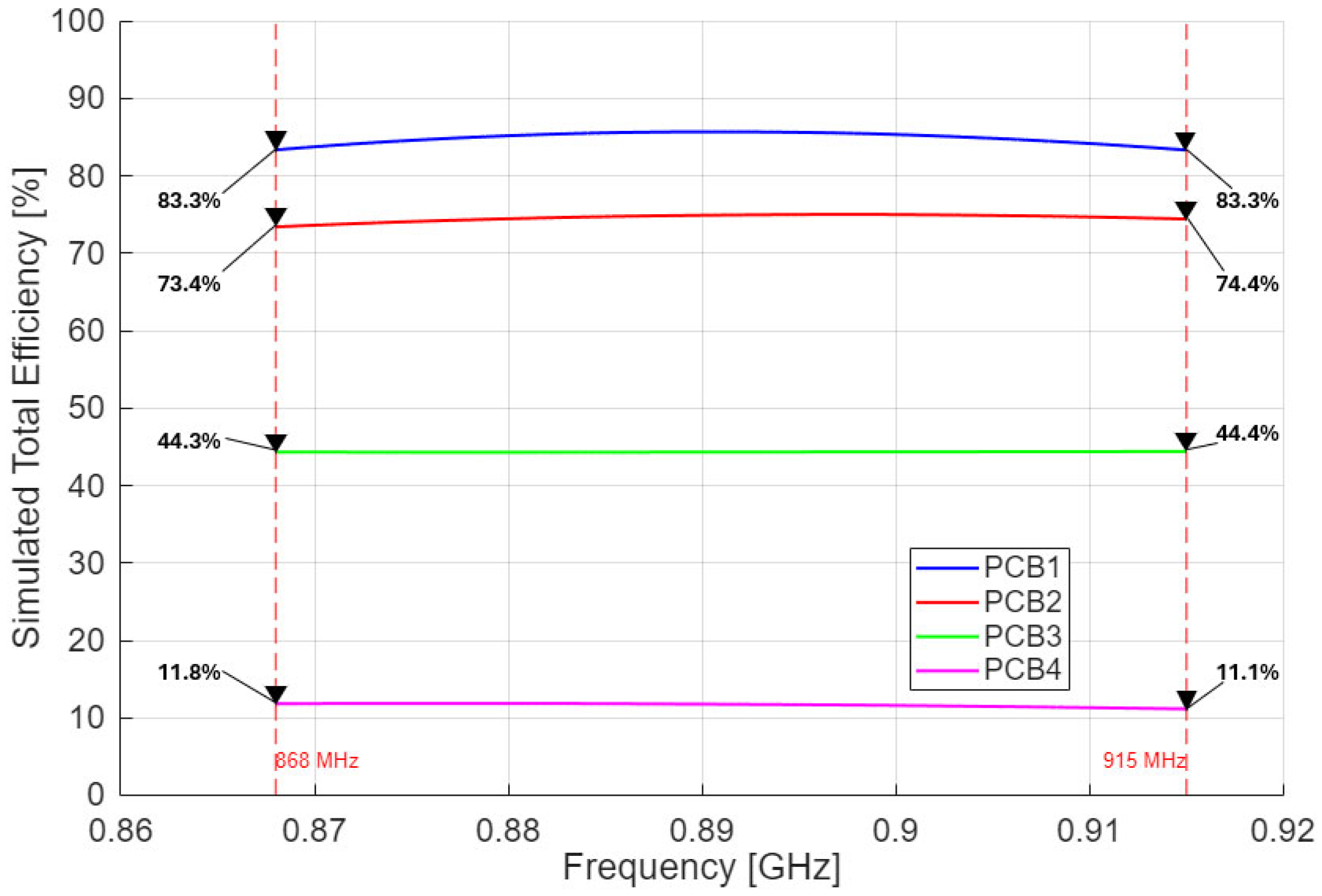
- PCB#1 was simulated with a nearly ideal matching network, providing below –15 dB across the 0.87–0.91 GHz band, with a minimum of −60 dB at 0.89 GHz. The mismatch loss in this case is negligible, yielding a simulated total efficiency exceeding 83% throughout the band.
- PCB#2 included a suboptimal matching network, maintaining an of approximately −10 dB over the same frequency range. This corresponds to a mismatch efficiency () of ~90%, leading to a simulated total efficiency above 73%.
- PCB#3 was designed with a constant of −3 dB. The mismatch efficiency in this case is limited to 50%, resulting in overall efficiency values of around 44%.
- PCB#4 represents a severely mismatched case, with close to −1.5 dB across the band. Only ~30% of the input power is accepted, reducing the total efficiency to approximately 11%.
In this work, all electromagnetic simulations and measurements are conducted within the 868–915 MHz frequency range. This span encompasses the most widely adopted sub-GHz bands for low-power wide-area (LPWA) wireless technologies, particularly NB-IoT and LTE-M, which are commonly used in battery-constrained IoT devices. These protocols rely on robust link budgets and high coverage performance, making antenna efficiency and impedance stability critical design parameters. Focusing the analysis on this frequency region, therefore, ensures relevance to practical IoT deployments while enabling a representative evaluation of how impedance mismatch affects both radiated performance and power-amplifier behaviour under real operating conditions.
The simulated responses of the four PCB configurations are shown in Figure 3, where the progressive degradation of impedance matching across the designs can be clearly observed. The corresponding simulated total efficiency curves are depicted in Figure 4, highlighting the reduction in radiated power efficiency as the worsens.
Figure 3.
Simulated of the four PCB configurations, illustrating the progressive degradation in impedance matching from PCB#1 (optimal) to PCB#4 (severely mismatched).
Figure 4.
Simulated total efficiency of the four PCB configurations, showing the strong dependence of radiated power on the quality of the impedance match.
In the case of PCB#4, which represents the most severely mismatched configuration, the simulated total efficiency drops to around 11%. This value is notably lower than the theoretical estimate of approximately 22% obtained from the mismatch-based efficiency calculation. Based on Figure 4, the total efficiency is ηt = 83.3% when the antenna system features an S11 < −16 dB. Therefore, based on Equation (2), ηr = 86.0%. Now, if S11 = −1.3 dB, based on the same Equation (2), ηt = 22.2%. However, the reality shows 11.8% (Figure 4). The reason for this is due to the losses of the matching network when the S11 is low, with a low antenna impedance that increases the current, and therefore increases the losses in the resistive part of the matching network.
For a basic antenna with an impedance R connected to a matching network comprising a series inductor with Rm as resistive losses, the ηm = R/(Rm + R). When the antenna is matched to values close to 50 Ω, an Rm = 3 Ω results in ηm = 94%. But when the antenna is poorly matched, for example, −1.3 dB, which may correspond to an R =3.8 Ω, the losses of the matching network are now ηm = 55%. Note that this is double the losses with respect to the well-matched case, explaining the low efficiency for the case when the antenna system corresponds to S11 = −1.3 dB [5].
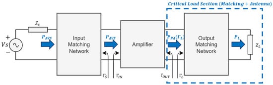
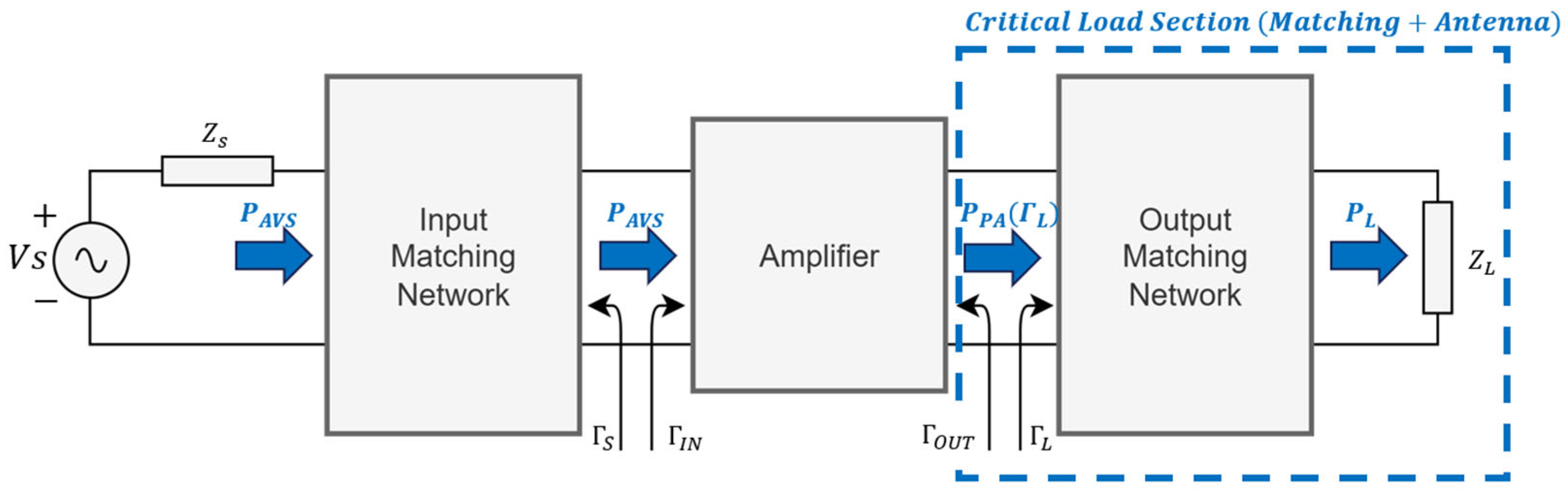
The expressions presented in Equations (1) and (2) assume an ideal radiofrequency source that delivers a constant-input-power Pavs irrespective of the antenna load impedance. In practical wireless transceivers, however, the power delivered to the antenna port is load-dependent. When the antenna impedance deviates from the nominal design value, the PA experiences load-pull effects that shift its operating point, modify its gain, and change the effective RF power available at its output. Consequently, the TRP of a real IoT device can be expressed in the general form (3):
where denotes the effective output power of the power amplifier under the reflection coefficient (Figure 5) (instead of the constant Pin used in the ideal case of Equation (2)), and η_t is the total efficiency defined previously.
Figure 5.
Block diagram of the transmitter front-end. The source is matched (), delivering constant available power . The blue dashed box highlights the critical load section (output matching network + antenna), which determines the load reflection coefficient and has the greatest impact on PA output power and total radiated power in IoT devices.
The term in Equation (3) represents the actual RF output power delivered by the power amplifier when its output is terminated with a load reflection coefficient . Unlike the constant input power assumed in the ideal case of Equation (2), is load-dependent. When the load impedance equals the optimum value (i.e., ), the PA delivers its maximum output power, so . For any other load condition, . Mathematically, this dependence is expressed as (4):
where [19] is the transducer power gain of the PA under load reflection coefficient , defined as (5):
(assuming the source is matched, ).
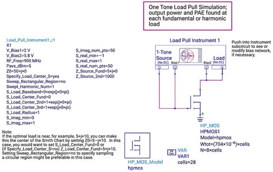
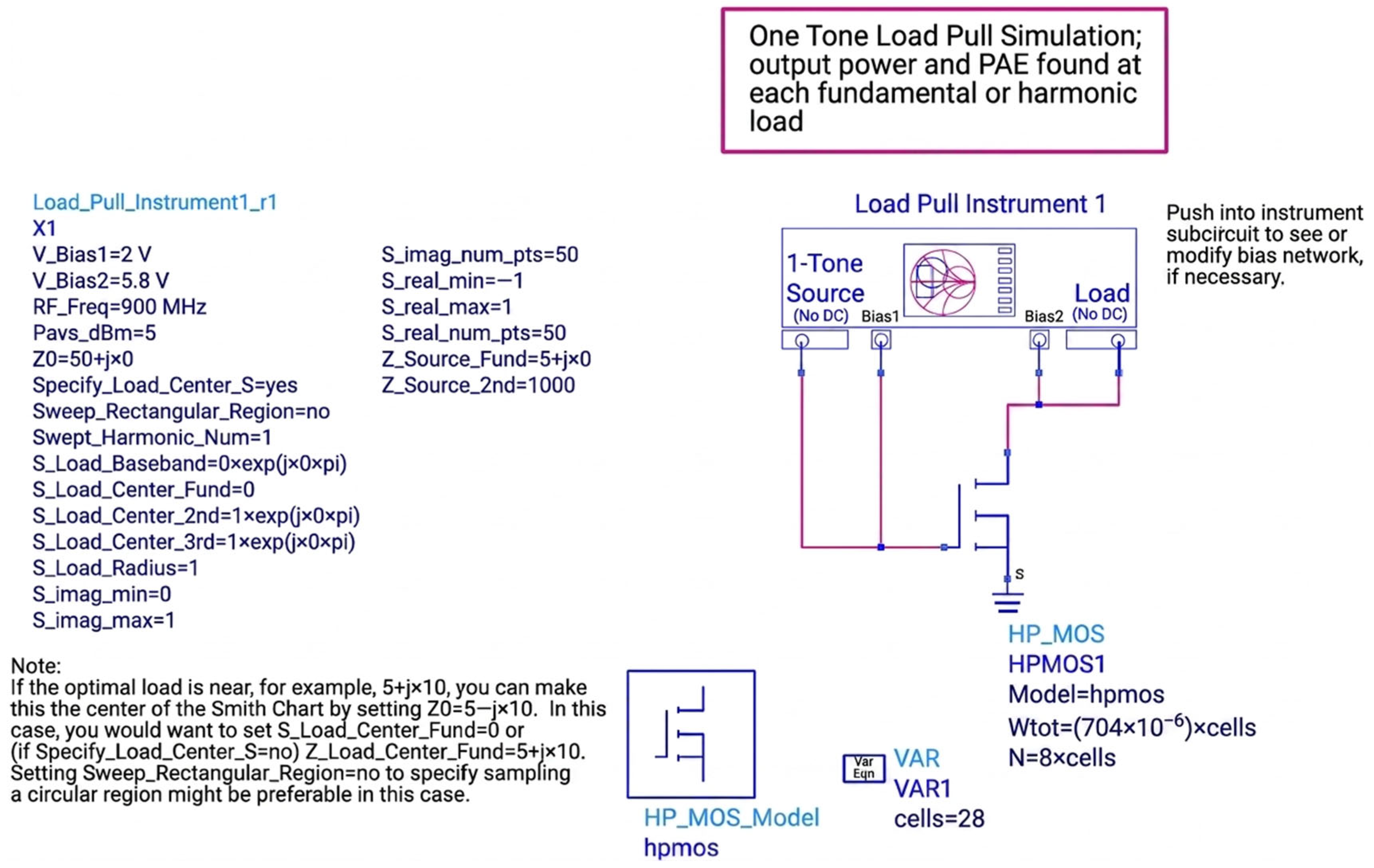
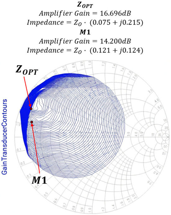
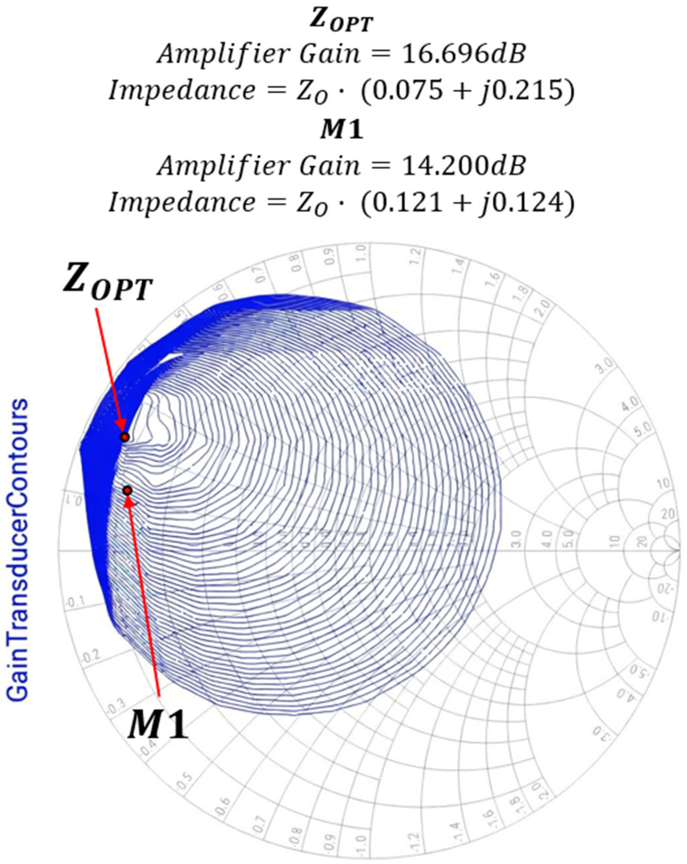
To quantitatively illustrate this dependence, a load-pull simulation was performed using a nonlinear FET model. The analysis consisted of a one-tone, constant available source power load-pull simulation at 900 MHz with an available input power and a source impedance of 50 Ω (). The circuit employed the HP_MOS nonlinear transistor model (hpmos) with a total gate width configured as 28 cells (), biassed at and . The load reflection coefficient was swept over a full circular region of the Smith chart (, , 50 × 50 sampling points), as shown in the complete simulation setup of Figure 6. Transducer power gain contours were extracted directly from the harmonic-balance results of the Load Pull Instrument.
Figure 6.
Schematic of the one-tone constant available source power load-pull simulation setup implemented.
Figure 7 shows the transducer power gain contours on the Smith chart. The maximum transducer gain of 16.7 dB is achieved at the optimum load impedance . In contrast, at the mismatched load point (corresponding to a voltage standing wave ratio VSWR = 6), the transducer gain drops to 14.2 dB. This represents a gain compression of 2.5 dB caused by the load-pull effects when the PA output is terminated with a highly reflective load. Such behaviour directly explains the reduction in expressed in Equation (4) and accounts for the additional efficiency losses observed in the active measurements with the SX1276 transceiver.
Figure 7.
Simulated transducer power gain contours on the Smith chart from load-pull analysis using a nonlinear FET model.
It is important to elaborate on how the 14.2 dB gain was obtained. For the optimal impedance, Zopt = 3.75 + j ·10.7 Ω, an output matching network (Figure 5) is designed to match to a 50 Ω antenna load. Then, an antenna with SWR = 6 is considered, with ZL = 50/6 Ω, while maintaining the same matching network. The resulting impedance at the output of the amplifier results in 50· (0.121 + j0.124) Ω. For this value, the gain, based on the load-pull analysis is 14.2 dB.
This quantitative characterisation using load-pull analysis explicitly links the reflection coefficient presented to the PA output with the resulting gain degradation, thereby providing a clear explanation for the additional loss mechanism captured in Equation (3).
3. Validation in Anechoic Chamber
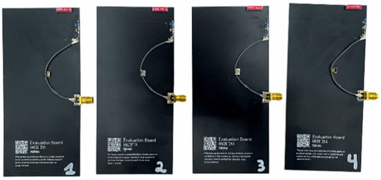
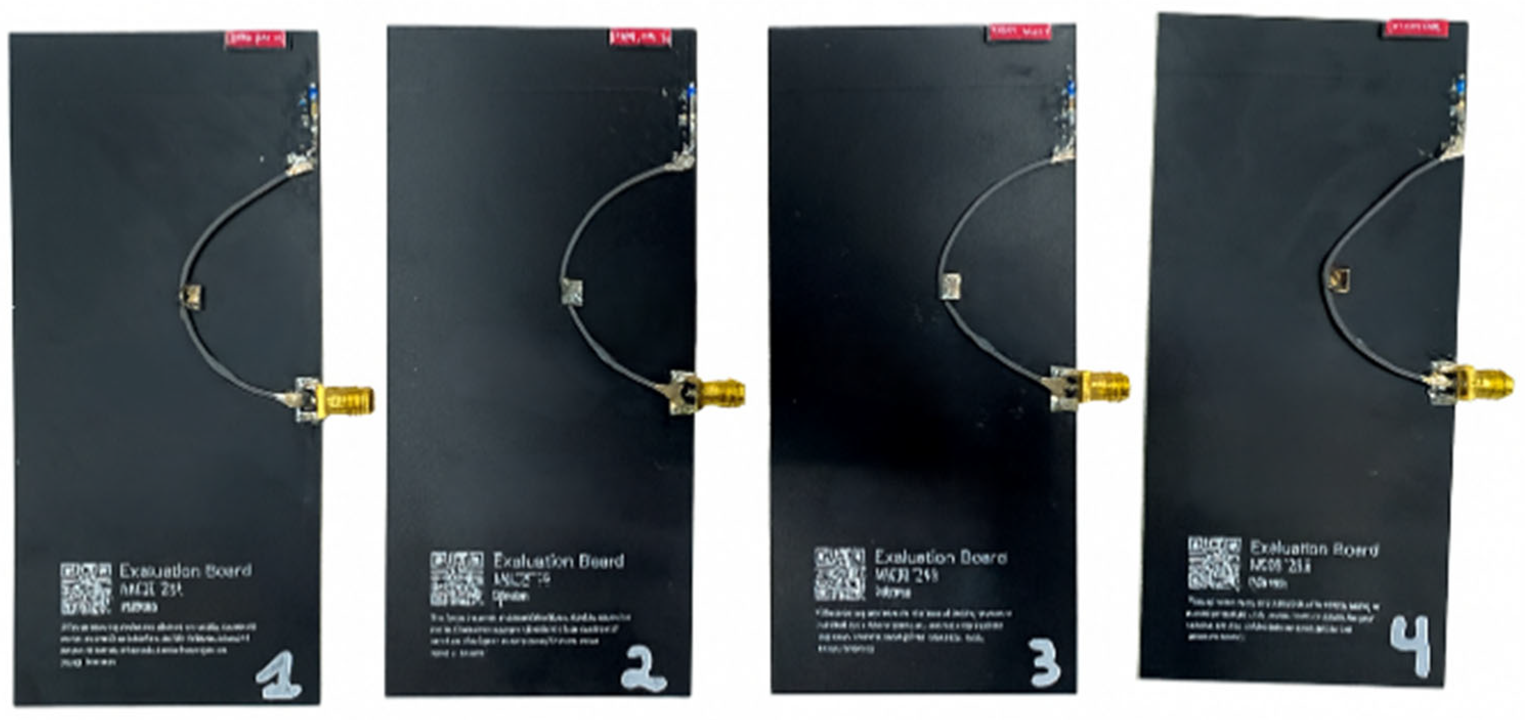
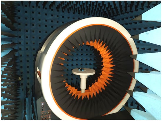
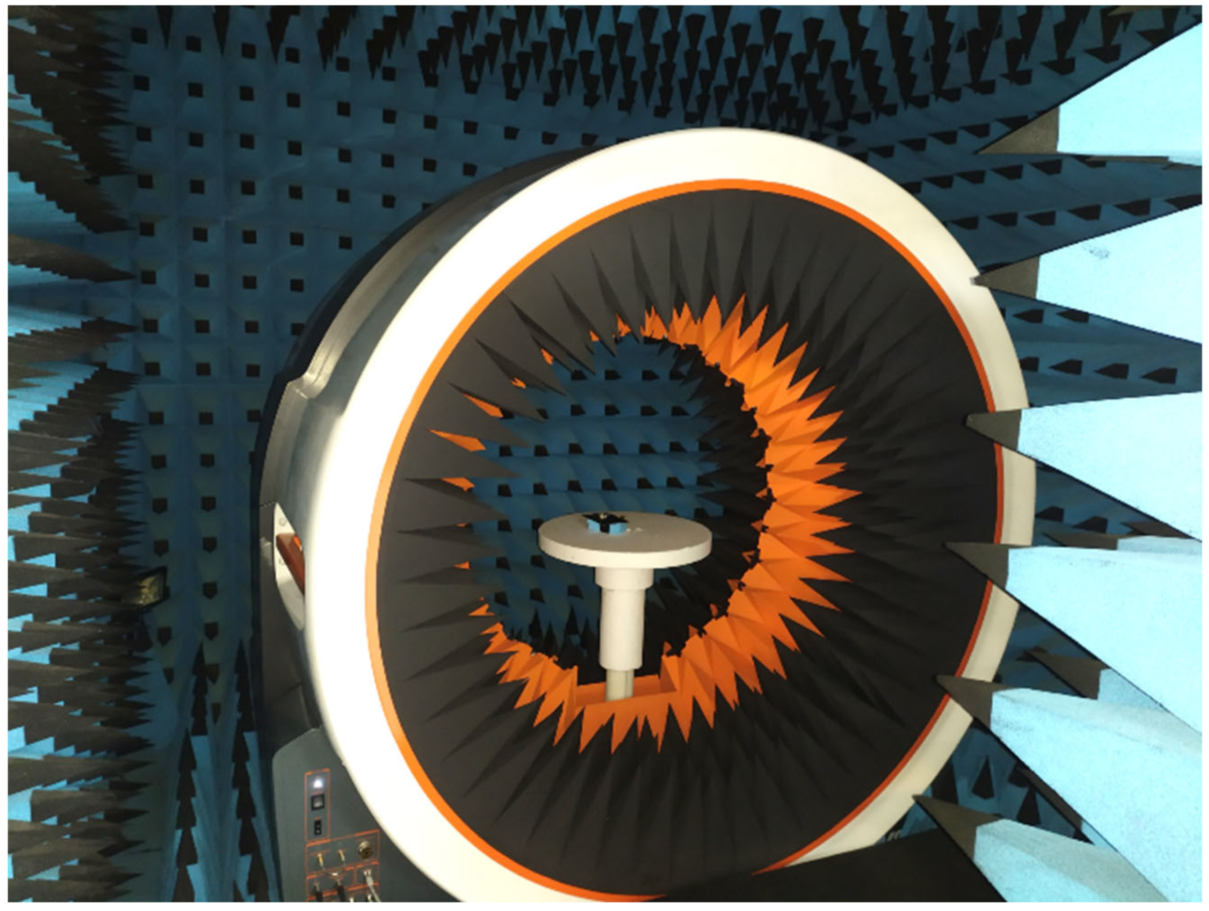
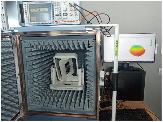
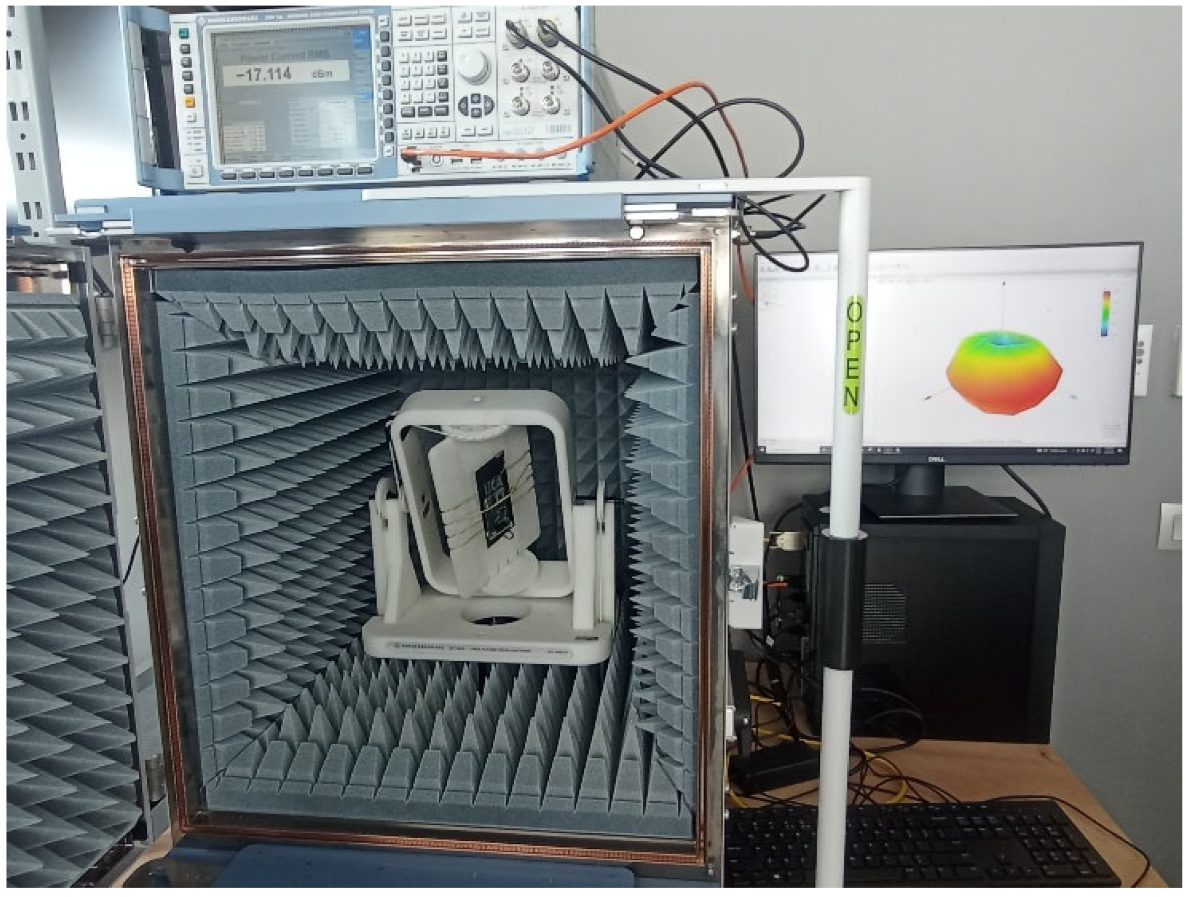
To validate the theoretical predictions presented in Section 2, the four PCB configurations were fabricated (Figure 8) and measured under controlled, idealised conditions using a Satimo StarLab [18] near-field measurement system (Figure 9). This experimental setup allows for precise characterisation of the total efficiency, minimising the influence of environmental factors and external perturbations [16,17].
Figure 8.
Fabricated PCB prototypes (1–4) employing identical antenna boosters but distinct impedance matching networks to evaluate mismatch effects on radiated performance.
Figure 9.
A near-field measurement system is used for antenna characterisation under controlled conditions.
To emulate impedance mismatch in the wireless device embedding the antenna due to external effects, each PCB integrates a distinct matching network designed to progressively degrade the impedance adaptation between the transmitter and the antenna booster element.
All four configurations share the same antenna booster PCB layout, including a 120 mm 60 mm ground plane, differing only in the values of the lumped components Z1–Z3 that define the impedance transformation, as summarised in Table 1. High-Q, tight-tolerance, surface-mount (SMD) components are employed in all networks to minimise parasitic effects and ensure consistent impedance behaviour across prototypes [20]. PCB#1 represents the optimally matched case, while PCBs 2–4 introduce increasing levels of mismatch by systematically modifying the inductance and capacitance of the matching network. This controlled variation allows for the impact of mismatch severity on the total radiated power and efficiency to be isolated, while keeping the radiating structure and feed conditions identical across all cases.
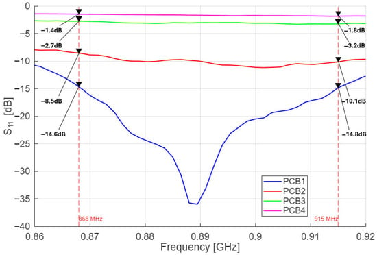
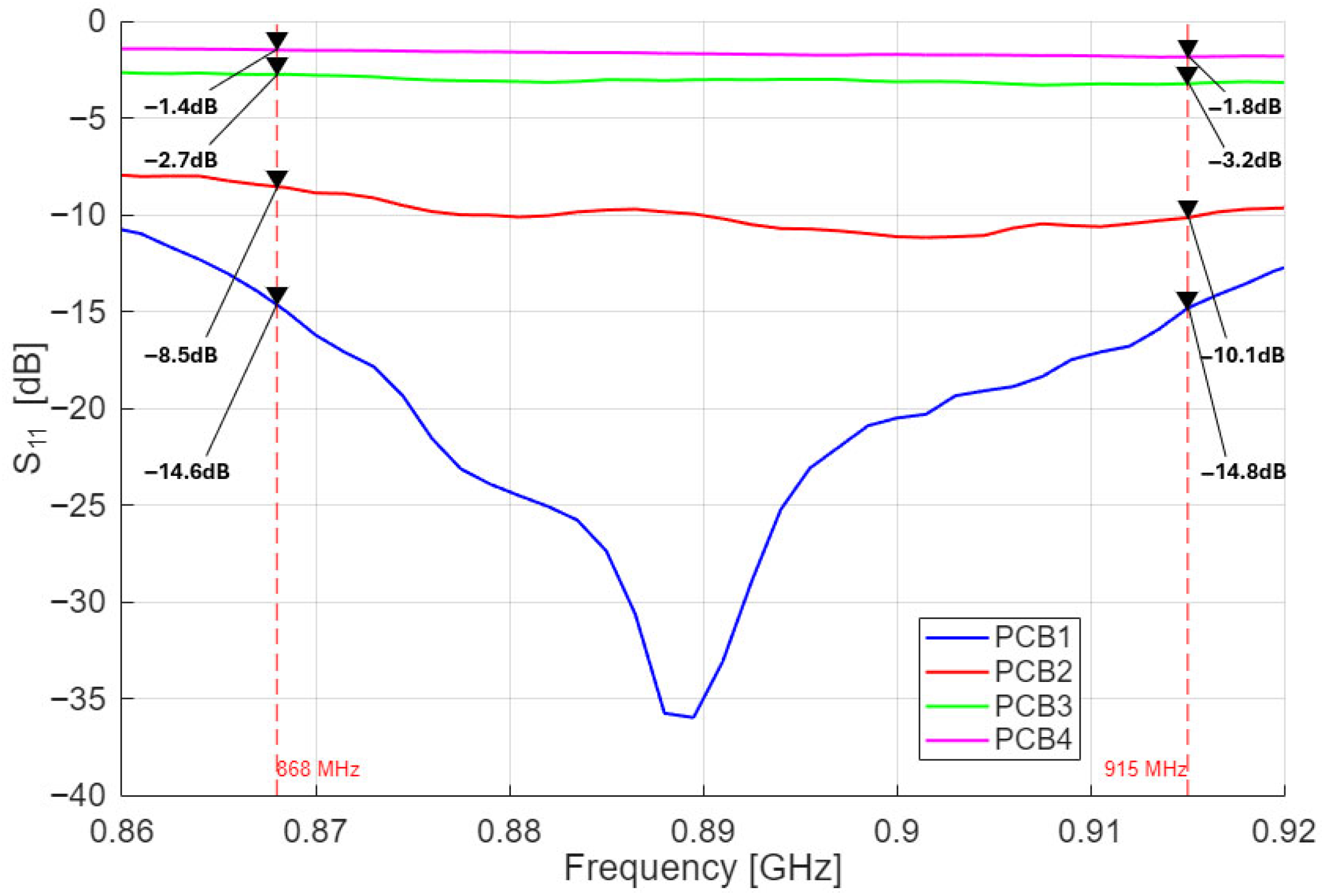
As expected, PCB#1 exhibits the best impedance matching across the 868–915 MHz band, with values consistently below −10 dB, confirming the effectiveness of the optimised matching network (Figure 10). PCB#2 maintains a moderate matching level, with varying between −7 dB and −11 dB over the same frequency range. PCB#3 presents a clearly degraded impedance adaptation, with remaining around −3 dB, indicating substantial reflection and limited power transfer to the antenna. Finally, PCB#4 corresponds to the most severe mismatch condition, with values close to −1.5 dB across the band, evidencing minimal power acceptance and dominant reflection at the input port. Note that the matching levels were intentionally adjusted to be the same as the simulated cases to be consistent with the comparison.
Figure 10.
Measured S11 for the four PCB configurations under ideal conditions.
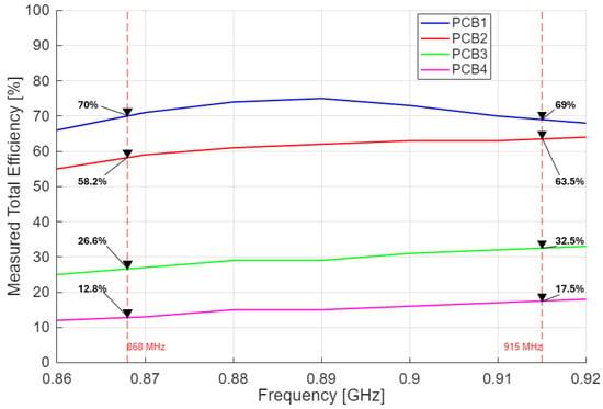
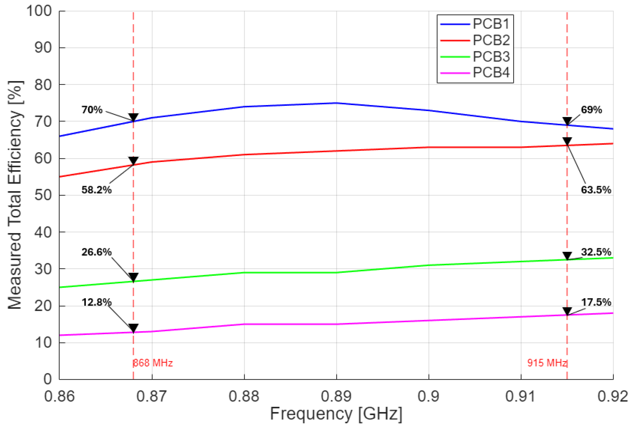
The total efficiency measured for each PCB is presented in Figure 11. The trends observed closely correlate with the behaviour. PCB#1 achieves the highest efficiency, ranging from 0.66 to 0.75 across the band, followed by PCB#2 (0.55–0.64), PCB#3 (0.25–0.33), and PCB#4 (0.12–0.18). These results confirm that even under ideal conditions, the quality of the matching network is a primary determinant of total radiated power. Minor discrepancies between theoretical predictions and measured data are attributed to fabrication tolerances, parasitic effects, and the intrinsic limitations of the measurement system.
Figure 11.
Measured total efficiency for the four PCB configurations under idealised conditions.
It is noteworthy that, in this controlled environment, the power amplifier used in an anechoic chamber system maintains a constant output power regardless of variations in antenna impedance. This is because the system is designed to operate with a variable load impedance, including the presence of a circulator, allowing the amplifier to maintain its output power by perceiving good matching regardless of the antenna impedance. This characteristic is critical for the accuracy of measurements conducted in the anechoic chamber, ensuring that the observed variations in radiated efficiency are primarily due to antenna characteristics and not fluctuations in amplifier output power [16].
Overall, these experimental results validate the theoretical framework introduced in Section 2. The correlation between and radiation efficiency is evident: as the improves, more input power is successfully radiated, while poor matching substantially reduces the effective radiated power. These findings emphasise the expected relationship between radiated power and impedance mismatch.
However, considering the practical case, in which the antenna is connected to a transceiver whose output impedance deviates from 50 Ω and no circulator is present to protect the power amplifier from load reflections, the following research questions arise: is the radiated power determined solely by the antenna impedance mismatch, or do additional mechanisms contribute? If additional losses are present, how significant are they? The following section addresses these questions.
4. Mismatch Effects in Realistic Environments
While Section 2 and Section 3 analysed antenna mismatch under simulated and controlled conditions, real-world operation introduces additional variables that can significantly modify the total radiated power. In practical scenarios, not only does the antenna experience impedance mismatch, but the power amplifier (PA) also suffers from gain degradation when operating with a non-ideal load. This combined effect leads to a further efficiency reduction beyond that predicted by simulations or passive measurements [5].
To investigate these effects, active measurements were conducted in a realistic test environment replicating the operational conditions of compact IoT devices. The same four PCB configurations described previously were evaluated. Each PCB included the same antenna booster and matching network topology, ensuring that performance variations were solely attributable to impedance mismatch and its impact on the PA [21]. The measurement setup is illustrated in Figure 12, showing the complete configuration used for active radiated power characterisation. Intentional antenna mismatch simulates real operating conditions, such as when the device is placed near a conductive object. For example, positioning the device on or close to a metallic surface can introduce impedance variations, with mismatch severity increasing as the distance decreases [22].
Figure 12.
Setup for active radiated power measurement using a Rohde & Schwarz DST200 anechoic chamber with a DST-8165 3D positioner.
Active measurements were performed using a compact anechoic test chamber (Rohde & Schwarz DST200), equipped with a fully automated 3D positioner (model DST-8165) that enables the characterisation of the TRP and then the extraction of the total efficiency of small wireless devices, since the injected power Pin is first measured in conductive mode. This setup provides a controlled electromagnetic environment with minimal reflections, ensuring accurate evaluation of the radiated performance. The chamber integrates a wideband measurement antenna and is connected to a vector signal analyser, which records the received power while the device under test (DUT) is automatically rotated in azimuth and elevation to obtain the full-sphere radiation pattern.
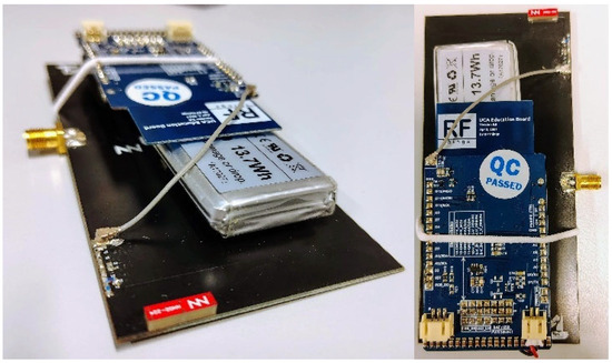
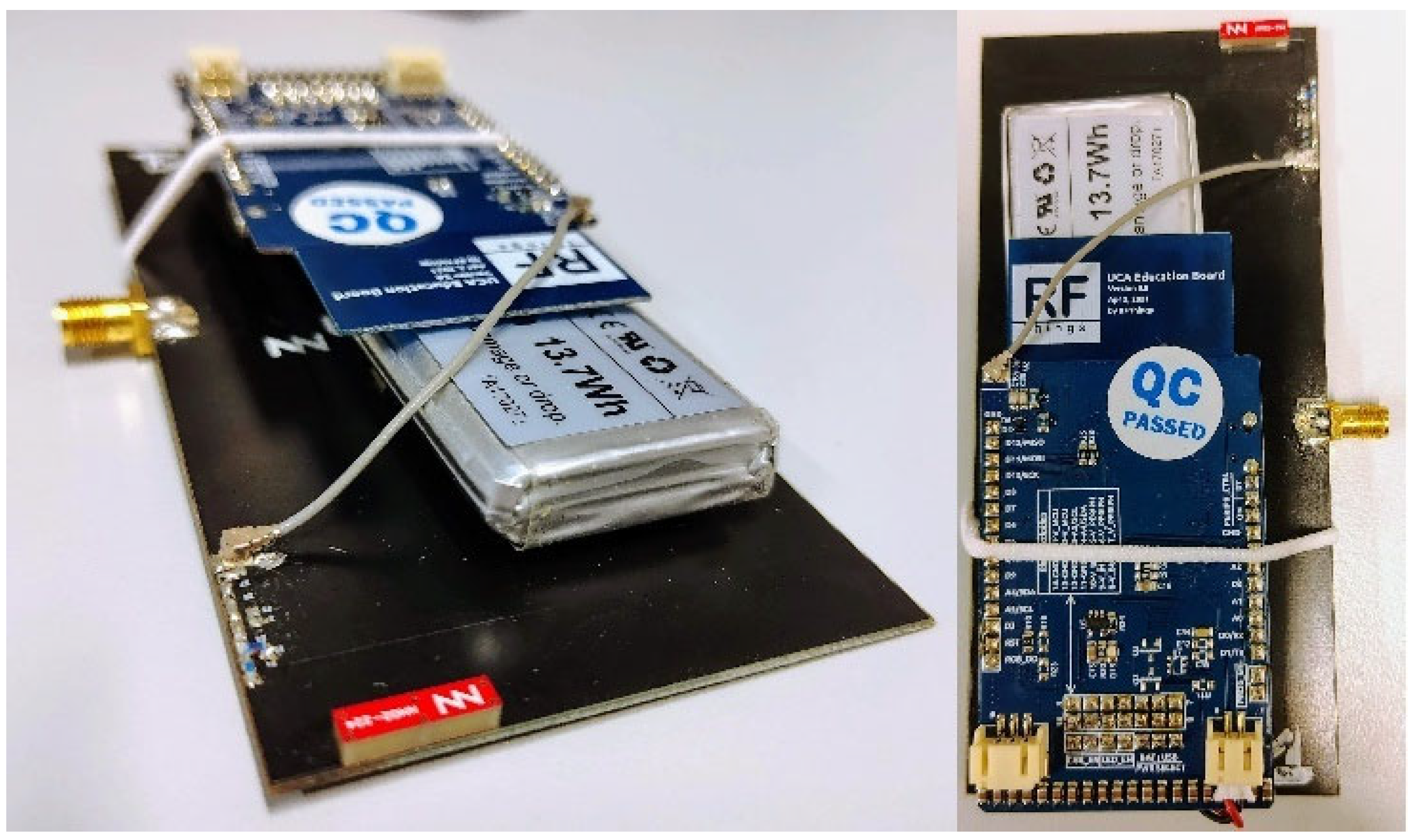
In these measurements, a UHF transceiver (SX1276) was configured to operate in continuous-wave (CW) transmit mode, thus enabling active characterisation. The transmitter was implemented on a separate PCB powered by a dedicated 13.7 Wh lithium battery, and it delivered the RF signal to the antenna booster through a UFL coaxial cable (Figure 13). The delivered power at the input of the matching network was measured (conductive mode). Since the input power is known, as well as the , the total efficiency is then calculated using (2).
Figure 13.
Prototype with an autonomous SX1276 transceiver and a Lithium battery.
Unlike passive measurements, which rely on network analyser-based S-parameter evaluation, active measurements capture the combined effects of antenna mismatch, power amplifier (PA) behaviour, and overall system losses. This methodology therefore provides a comprehensive and realistic assessment of how impedance mismatch impacts the effective radiated power of the complete transmitter system.
TRP and total efficiency were measured at two representative frequencies, 868 MHz and 915 MHz. The results are summarised in Table 2. For all active measurements, the battery voltage was monitored and verified to remain constant during the measurement procedure, thereby excluding supply voltage variations as a source of TRP degradation.
Table 2.
Active results.
These active measurements provide a complete characterisation of the radiated performance of the four PCB configurations under realistic excitation conditions. The obtained values of TRP and total efficiency incorporate not only the effects of antenna mismatch but also any variations in the effective gain of the transmitter chain when operating with non-ideal load impedances. Consequently, the results presented in this section constitute a comprehensive experimental baseline for evaluating how impedance mismatch affects the overall power transfer in practical wireless devices. The analysis and interpretation of these findings, as well as their implications for system design and performance optimisation, are discussed in detail in Section 5.
5. Discussion and Implications
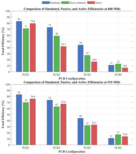
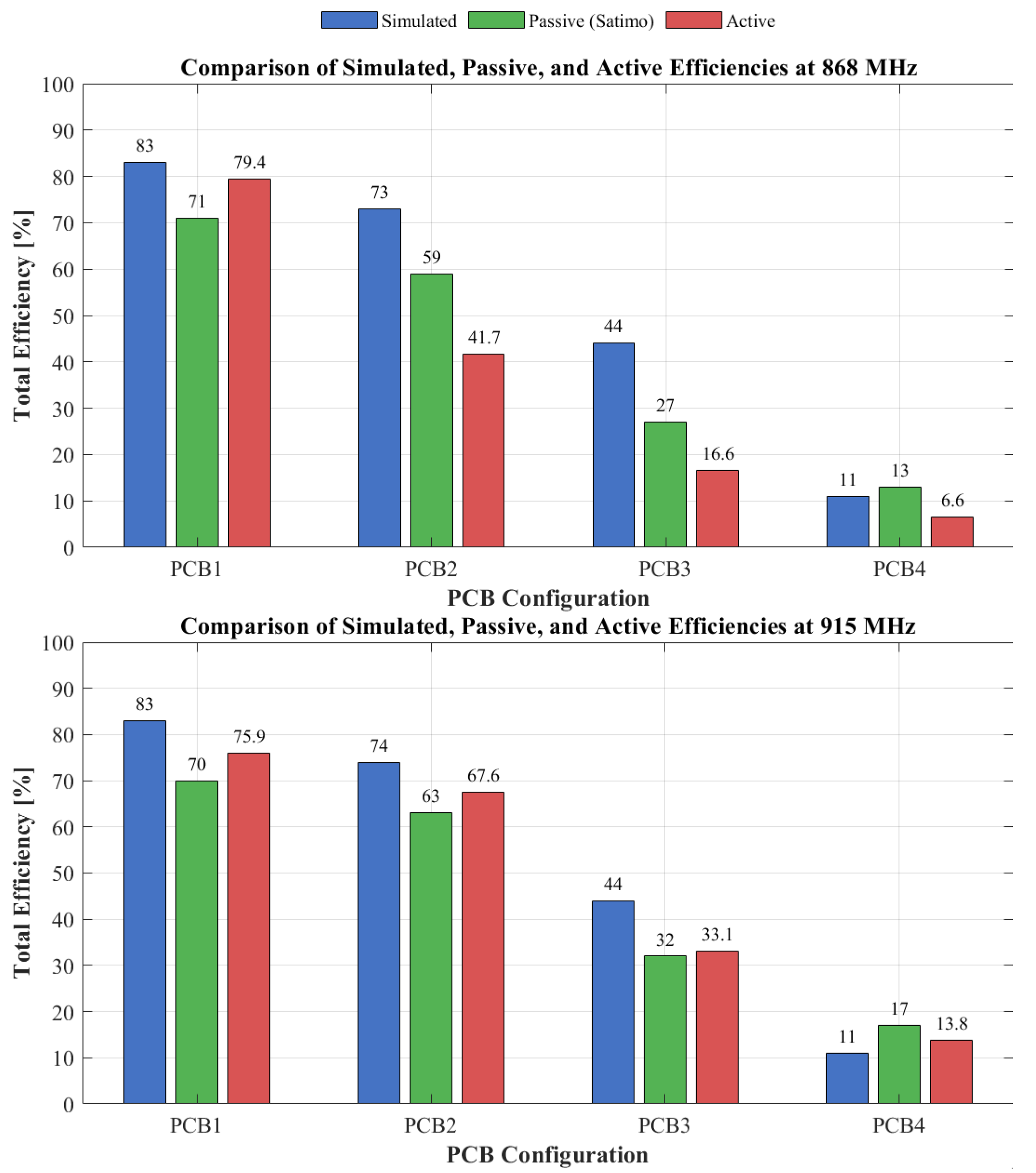
To better understand the combined influence of impedance mismatch and amplifier gain degradation, Figure 14 summarises the measured and simulated total efficiencies for the four PCB configurations at 868 MHz and 915 MHz. The figure compares the efficiencies obtained from full-wave simulations, passive measurements in the anechoic chamber, and active measurements performed under realistic excitation conditions. This representation highlights the progressive degradation in total efficiency as the impedance mismatch increases from PCB#1 to PCB#4.
Figure 14.
Simulated, passively measured, and actively measured total efficiencies for the four PCB configurations at 868 MHz and 915 MHz.
A closer inspection of Figure 14 reveals that while both simulated and passive results follow a consistent trend across the four configurations, a noticeable discrepancy appears for PCB#3 at 868 MHz. In this case, the efficiency measured in the anechoic chamber is significantly lower than the simulated (2.1 dB), even though the same matching network topology and component values were used.
At 915 MHz, however, the agreement between simulated and passive efficiency results is considerable, suggesting that the model accuracy increases as the antenna operates closer to its resonance. The active measurements, on the other hand, show a systematic reduction in efficiency for PCB#3 and PCB#4, consistent with the expected amplifier gain degradation under severe mismatch. This behaviour confirms that, beyond the electromagnetic mismatch alone, nonlinear effects in the power amplifier become dominant when the load impedance deviates significantly from the nominal value. These results underscore the importance of co-design approaches that jointly consider the antenna and the transceiver behaviour to ensure predictable performance across frequency and load variations.
The close agreement between simulation and passive measurements validates the theoretical framework established in Section 2, confirming that, under idealised excitation, the total radiated power is primarily governed by antenna mismatch and ohmic losses in the matching network.
A detailed comparison between passive and active total efficiencies is summarised in Table 3, which highlights the impact of amplifier loading under varying impedance mismatch conditions. The discrepancies are especially significant at 868 MHz, where the most severely mismatched configurations exhibit substantial degradation: PCB#3 loses 2.1 dB, while PCB#4 shows a nearly 3 dB reduction relative to their passive references. These results indicate that nonlinear PA loading becomes dominant under strong impedance mismatch at the lower operating frequency. In contrast, at 915 MHz, the active–passive deviations are generally smaller, reflecting the reduced sensitivity of the transmitter to mismatch closer to the antenna’s resonance. Across both frequencies, the trend clearly confirms that the deviation systematically increases with mismatch severity, whereas well-adapted configurations (PCB#1–PCB#2) maintain close agreement. This behaviour underscores the combined influence of electromagnetic mismatch and PA nonlinearities on the radiated performance. As previously documented in the literature [13,22], such deviations arise from the sensitivity of PA gain to highly reflective loads, a mechanism consistent with the degradation observed in the most mismatched configurations.
Table 3.
Active/Passive Total Efficiency () Deviation.
The additional efficiency reduction observed in the active measurements (see Table 3) originates from the nonlinear response of the power amplifier to the mismatched load. When a high reflection coefficient || is presented to the PA output, the reflected power alters the effective load impedance seen by the final stage, shifting the dynamic load line away from the optimum power match. This load-pull effect causes gains in compression, increased internal power dissipation, and a reduction in the effective RF power delivered by the amplifier, . In the present study, these mechanisms produce extra efficiency drops of up to 2.9 dB at 868 MHz for the most severely mismatched case (PCB#4), which cannot be explained by radiative mismatch alone. Such behaviour is consistent with the load-pull results reported for similar low-power CMOS PAs [8,13,22], where gain reductions of 2–4 dB are typically observed for VSWR values between 3:1 and 10:1.
When the antenna presents a severe mismatch, the reflected power returning to the amplifier alters its load line, modifying the effective output impedance and shifting the operating point away from the region of optimal efficiency and linearity. This interaction causes a reduction in available gain and an increase in internal power dissipation, resulting in a lower effective radiated power. This effect is particularly pronounced in compact transmitter architectures, where thermal management and bias stabilisation are limited. Consequently, the observed loss of total efficiency in PCB#3 and PCB#4 during active operation results from the combined effects of radiative mismatch and amplifier gain compression [13,15,16].
These results provide direct experimental evidence that, in practical devices, the total radiated power cannot be accurately predicted from passive antenna measurements alone. Even if the reflection coefficient and passive efficiency are known, the active behaviour of the power amplifier under non-ideal loading introduces an additional and often dominant loss mechanism. This observation has important implications for the design and characterisation of low-power wireless systems: both the antenna and the amplifier must be jointly optimised to ensure stable and efficient operation under varying impedance conditions [21,23].
Although the present study focuses on antenna booster technology with simple matching networks, the conclusions regarding the combined effect of radiative mismatch and PA gain degradation under realistic load conditions extend to other antenna technologies [24].
Accordingly, mitigation strategies include adaptive impedance tuning, reconfigurable antennas, fast VSWR protection loops, and robust PA architectures (balanced/quasi-balanced, Doherty variants) that improve mismatch resilience [15,16,17,25].
6. Conclusions
This work has quantitatively demonstrated the dual impact of antenna impedance mismatch and power amplifier gain degradation on the total radiated power of wireless devices. Through a combined theoretical, passive, and active experimental approach, it was shown that while simulations and anechoic measurements accurately predict the radiative mismatch losses, they fail to capture the additional degradation that occurs in real operating conditions when the amplifier interacts with a non-ideal load.
From a system-level perspective, the total radiated power of an active transmitter can be expressed as Equation (3), where denotes the effective RF power generated by the power amplifier when operating under a load characterised by the reflection coefficient . Importantly, unlike the classical assumption of a load-independent RF source, is not constant and deviates from its nominal value when due to load-line displacement, nonlinear operation, and internal loss mechanisms within the PA.
The active measurements revealed that, particularly for highly mismatched configurations, the effective efficiency and TRP deteriorate well beyond what can be explained by reflection losses alone. These results provide clear experimental evidence that amplifier gain compression under reflective loading constitutes a significant, often dominant, loss mechanism in compact wireless platforms. Consequently, evaluating only the antenna performance in isolation is insufficient for accurately predicting the radiated power of real devices.
For the IoT domain—where devices are typically small, cost-constrained, and energy-limited—these findings highlight the critical importance of implementing adaptive impedance management strategies. Techniques such as tuneable matching networks, reconfigurable antennas, and feedback-based amplifier control can dynamically maintain the optimal load conditions required for efficient power transfer. Additionally, system-level co-design approaches that jointly optimise the antenna and the PA are essential to ensure robustness against user interaction, environmental variation, and manufacturing tolerances.
The main contribution of this work lies in the quantitative separation and superposition of the two distinct mismatch mechanisms—radiative losses due to antenna and matching-network impedance mismatch, and the additional degradation of power amplifier gain under non-ideal load conditions—within the same unified experimental framework using identical antenna boosters. By comparing passive (ideal source) and active (real transceiver) measurements on the same prototypes, we demonstrate that passive antenna characterisation alone can underestimate the total efficiency loss by up to 2.9 dB in severely mismatched cases. This highlights that a realistic evaluation of radiated power in IoT devices must jointly consider both effects. Ultimately, achieving high radiated efficiency in real devices demands a holistic co-design perspective in which the antenna, matching network, and power amplifier are treated as an integrated system rather than independent components. Such an approach is essential for enabling energy-efficient, reliable, and scalable wireless communication in future IoT and low-power radio systems.
Author Contributions
Conceptualisation, A.O., J.A. and J.N.; Methodology, A.O., A.A. and J.A.; Writing—original draft, A.O. and F.F.; Writing—review and editing, A.O., J.N. and J.A.; Supervision, J.A., J.N. and F.F. Data curation, G.F. and F.F. All authors have read and agreed to the published version of the manuscript.
Funding
This work was partly supported by the Spanish Ministry of Science and Innovation under grant CPP 2022-010034.
Data Availability Statement
The original contributions presented in this study are included in the article. Further inquiries can be directed to the corresponding author.
Conflicts of Interest
Authors Gerard Fleta, Aurora Andújar and Jaume Anguera were employed by the company Ignion. The remaining authors declare that the research was conducted in the absence of any commercial or financial relationships that could be construed as a potential conflict of interest.
References
- Zanella, A.; Bui, N.; Castellani, A.; Vangelista, L.; Zorzi, M. Internet of Things for smart cities. IEEE Internet Things J. 2014, 1, 22–32. [Google Scholar] [CrossRef] [Scilit]
- Sharma, S.K.; Wang, X. Toward Massive Machine Type Communications in Ultra-Dense Cellular IoT Networks: Current Issues and Machine Learning-Assisted Solutions. IEEE Commun. Surv. Tutor. 2020, 22, 595–615. [Google Scholar] [CrossRef] [Scilit]
- Balanis, C.A. Antenna Theory: Analysis and Design, 4th ed.; John Wiley & Sons: Hoboken, NJ, USA, 2016. [Google Scholar]
- Raghunandan, K. Antennas, transmission lines, matching networks. In Introduction to Wireless Communications and Networks: A Practical Perspective; Springer International Publishing: Berlin/Heidelberg, Germany, 2022; pp. 339–377. [Google Scholar] [CrossRef] [Scilit]
- Anguera, J.; Andújar, A. Antenna Booster Technology for Wireless Communications; Institution of Engineering and Technology: Stevenage, UK, 2024; ISBN 978-1-83953-300-6. [Google Scholar] [CrossRef] [Scilit]
- Garg, R.; Bhartia, P.; Bahl, I.; Ittipiboon, A. Microstrip Antenna Design Handbook; Artech House: Norwood, MA, USA, 2001. [Google Scholar]
- Lizzi, L.; Ferrero, F.; Ribero, J.-M.; Staraj, R. Light and Low-Profile GSM Omnidirectional Antenna. IEEE Antennas Wirel. Propag. Lett. 2012, 11, 1146–1149. [Google Scholar] [CrossRef] [Scilit]
- Zenteno, E.; Isaksson, M.; Händel, P. Output impedance mismatch effects on the linearity performance of digitally predistorted power amplifiers. IEEE Trans. Microw. Theory Tech. 2015, 63, 754–765. [Google Scholar] [CrossRef] [Scilit]
- Ponte, J.; Ghahremani, A.; Huiskamp, M.; Annema, A.-J.; Nauta, B. Theory and Implementation of a Load-Mismatch Protective Class-E PA System. IEEE Trans. Circuits Syst. I Regul. Pap. 2020, 67, 369–377. [Google Scholar] [CrossRef] [Scilit]
- Fu, J.S.; Mortazawi, A. Improving power amplifier efficiency and linearity using a dynamically controlled tunable matching network. IEEE Trans. Microw. Theory Tech. 2008, 56, 3239–3244. [Google Scholar] [CrossRef] [Scilit]
- Liu, C.H.; Wang, R.L.; Su, Y.K.; Tu, C.H.; Juang, Y.Z. Performance degeneration of CMOS RF power cells after hot-carrier and load mismatch stresses. In Proceedings of the 2007 50th Midwest Symposium on Circuits and Systems, Montreal, QC, Canada, 5–8 August 2007; pp. 1062–1065. [Google Scholar] [CrossRef] [Scilit]
- Katz, A.; Wood, J.; Chokola, D. The evolution of PA linearization: From classic feedforward and feedback through analog and digital predistortion. IEEE Microw. Mag. 2016, 17, 32–40. [Google Scholar] [CrossRef] [Scilit]
- Quan, X.; Guo, Y.; Zhu, A. Effect and adaptive correction of impedance mismatch between antenna and power amplifier on digital predistortion. In Proceedings of the IEEE MTT-S International Microwave Symposium, Paris, France, 16–19 June 2013; pp. 1–3. [Google Scholar] [CrossRef] [Scilit]
- Carrara, F.; Presti, C.D.; Scuderi, A.; Santagati, C.; Palmisano, G. A methodology for fast VSWR protection implemented in a monolithic 3-W 55% PAE RF CMOS power amplifier. IEEE J. Solid-State Circuits 2008, 43, 2057–2066. [Google Scholar] [CrossRef] [Scilit]
- Sinha, S.S.; Rao, C.V.N.; Pujara, D. Balanced power amplifier protection against load mismatch. IEEE Microw. Wirel. Compon. Lett. 2018, 28, 693–695. [Google Scholar] [CrossRef] [Scilit]
- Lyu, H.; Chen, K. Wideband quasi-balanced Doherty power amplifier with reciprocal main/auxiliary setting and mismatch-resilient parallel/series reconfiguration. In Proceedings of the 2021 IEEE MTT-S International Microwave Symposium (IMS), Atlanta, GA, USA, 7–25 June 2021; pp. 736–739. [Google Scholar] [CrossRef] [Scilit]
- Pozar, D.M. Microwave Engineering: Theory and Techniques, 4th ed.; John Wiley & Sons: Hoboken, NJ, USA, 2021. [Google Scholar]
- Microwave Vision Group (MVG). STARLAB—The Scalable, Trusted Platform for What’s Next in Antenna Testing [Product Datasheet]. 2025. Available online: https://www.mvg-world.com/media/3034/download/reference (accessed on 5 November 2025).
- Gonzalez, G. Microwave Transistor Amplifiers: Analysis and Design, 2nd ed.; Prentice Hall: Hoboken, NJ, USA, 1997. [Google Scholar]
- Murata Manufacturing Co. Ltd. SimSurfing: Component Data and Simulation Tool. 2025. Available online: https://ds.murata.com/simsurfing/index.html?lcid=en-us (accessed on 8 November 2025).
- Argaez-Ramirez, R.; Perez-Cisneros, J.R.; Fager, C. Investigation of power amplifier performance under load mismatch conditions. In Proceedings of the 2021 IEEE Topical Conference on RF/Microwave Power Amplifiers for Radio and Wireless Applications (PAWR), San Diego, CA, USA, 17–20 January 2021; pp. 41–43. [Google Scholar] [CrossRef] [Scilit]
- Fernández, A.; Andújar, A.; Pijoan, J.L.; Anguera, J. Reconfigurable Multiband Antenna Booster Architecture for Different Environments. IEEE Access 2023, 11, 85537–85548. [Google Scholar] [CrossRef] [Scilit]
- Scuderi, A.; Greco, A.; Neri, B.; Rizzo, S.A. Active load–pull techniques for power amplifier characterization. In Proceedings of the IEEE MTT-S International Microwave Symposium, Philadelphia, PA, USA, 8–13 June 2003. [Google Scholar]
- Wang, S.; Wang, W.; Chung, K.L.; Zheng, Y. An Orthogonal Quad-Beam Scanning Antenna Using 1-Bit Dielectric Modulation in Plasmonic Metamaterial Transmission Line for Traffic Monitoring Applications. IEEE Trans. Veh. Technol. 2025, 75, 2159–2168. [Google Scholar] [CrossRef] [Scilit]
- Alibakhshikenari, M.; Virdee, B.S.; Azpilicueta, L.; See, C.H.; Abd-Alhameed, R.; Althuwayb, A.A.; Falcone, F.; Huynen, I.; Denidni, T.A.; Limiti, E. Optimum power transfer in RF front-end systems using automatically tuned LC impedance matching networks. Sci. Rep. 2021, 11, 11825. [Google Scholar] [CrossRef] [Scilit] [PubMed]

Disclaimer/Publisher’s Note: The statements, opinions and data contained in all publications are solely those of the individual author(s) and contributor(s) and not of MDPI and/or the editor(s). MDPI and/or the editor(s) disclaim responsibility for any injury to people or property resulting from any ideas, methods, instructions or products referred to in the content. |
© 2026 by the authors. Licensee MDPI, Basel, Switzerland. This article is an open access article distributed under the terms and conditions of the Creative Commons Attribution (CC BY) license.