


Abstract
This study introduces two compact wideband substrate-integrated waveguide (SIW) filters fabricated using thin-film technology. The wideband bandpass response is achieved by incorporating interdigital capacitor (IDC) structures into a half-mode SIW (HMSIW) transmission line. An equivalent LC circuit model is formulated to analyze the influence of IDC parameters on the generation of transmission zeros. For the first filter (BPF 1), a third-order IDC coupling configuration is employed, resulting in a 1 dB passband spanning 11 GHz to 18 GHz, a minimum insertion loss of 0.66 dB, three transmission zeros that enhance stopband performance, and a compact core dimension of . For further miniaturization, a modified HMSIW transmission line incorporating a metal-insulator-metal (MIM) capacitor at the equivalent magnetic wall is proposed. This design effectively reduces the transverse dimension of the waveguide while maintaining the original cutoff frequency. Utilizing this configuration, the second bandpass filter (BPF 2) was designed and fabricated employing double-layer ceramic thin-film technology. The resulting filter exhibits a 1 dB passband spanning 10 GHz to 18 GHz, a compact footprint measuring , a minimum insertion loss of 0.58 dB, and features three transmission zeros. The fabricated and measured results of both filters show good agreement with simulations. Compared with previously reported wideband SIW filters, the proposed designs demonstrate comprehensive advantages in fractional bandwidth, insertion loss, out-of-band suppression, and circuit size, providing effective filtering solutions for high-density integration of microwave and millimeter-wave RF systems.
1. Introduction
The rapid advancement of 5G and 6G mobile communication technologies, alongside satellite communications and millimeter-wave technologies, is driving the development of contemporary wireless communication systems toward wideband capabilities, higher frequency operation, and increased integration [1,2,3,4]. The continuous improvement of system transmission rates and channel capacities imposes more stringent requirements on core devices in radio frequency (RF) front-ends. As a key frequency-selective module, filters urgently need to achieve a wide operating bandwidth while maintaining compact structure, low loss, and high stability. Substrate-integrated waveguide (SIW) combines the advantages of traditional metallic waveguides and planar circuits, featuring high Q-factor, low insertion loss, excellent electromagnetic shielding, and easy integration with planar circuits, making it an ideal structure for constructing high-performance microwave and millimeter-wave devices [5]. In recent years, the requirements posed by next-generation communication systems have driven significant research interest toward the development of broadband and miniaturized SIW filters [6,7,8].
One effective method for achieving broadband performance in SIW filters involves leveraging the inherent high-pass properties of SIW transmission lines in conjunction with bandstop structures to design broadband filters. In reference [9], a broadband filter with a fractional bandwidth of 62% was achieved by etching a pair of T-shaped defected ground structures (DGSs) on an SIW transmission line, with a size of 0.248 (where is the guided wavelength at the filter center frequency in the substrate). Reference [10] presents a broadband bandpass filter that integrates the substrate-integrated waveguide technology with spoof surface plasmon polariton (SSPP) structures. The passband frequency can be flexibly tuned by modifying the geometric parameters of both the SIW and SSPP components. The designed filter demonstrates a 3 dB fractional bandwidth of approximately 45.8%, with a compact overall size measuring . In reference [11], a hybrid broadband filter based on dual-slot loaded half-mode folded ridge SIW was reported, featuring both wide bandwidth and high selectivity. In this design, the lowpass and highpass cutoff frequencies could be independently controlled by adjusting the quasi-periodic slots and half-mode substrate-integrated waveguide (HMSIW) dimensions, and the stopband was further extended by etching an I-shaped pattern on the bottom layer. The measured results showed a passband covering 3.86–8.3 GHz with a size of . Reference [12] presents a compact broadband bandpass filter characterized by high selectivity, which is designed utilizing substrate-integrated waveguide technology in conjunction with DGS techniques. The broadband filtering response is attained through the incorporation of two inverted tuning-fork-shaped DGS elements positioned at the base of the SIW cavity. These DGS components serve to improve the performance of the upper stopband. The proposed filter demonstrates a fractional bandwidth of 19% and an insertion loss of approximately 1.2 dB. However, the overall device occupies an area of 1.93 . Broadband substrate-integrated waveguide filters, which are realized by cascading SIW components with bandstop elements, can effectively attain wide bandwidths while maintaining relatively low insertion loss within the passband. Nevertheless, these broadband filters frequently exhibit limited out-of-band rejection and tend to have considerable physical dimensions.
The multimode resonator (MMR) approach applied to substrate-integrated waveguide technology employs several closely spaced resonant modes within a single resonant cavity to achieve broadband performance. By meticulously engineering the resonant cavity structure, the resonant frequencies of multiple modes can be aligned in close proximity, resulting in the overlap of their resonance curves and the formation of a continuous, flat, and wide passband. The critical aspect of this methodology is the precise regulation and optimization of the coupling among the various modes within the resonant cavity. Presently, this technique has emerged as a central area of research in the development of broadband filters and has been extensively utilized in filter design [13,14,15]. In reference [16], a fifth-order compact broadband filter based on a U-slotted SIW cavity was proposed, where multimode resonators were formed by etching U-shaped slots on the metal surface of the SIW cavity, achieving broadband characteristics while significantly reducing circuit size. Compared with traditional single-mode SIW filters, the designed fifth-order SIW filter achieved a size reduction of 2.5 times, with a 3 dB fractional bandwidth of 42%, minimum in-band insertion loss of 1.1 dB, and overall size of . In reference [17], a broadband bandpass filter based on a planar dual-mode SIW cavity loaded with perturbation slots was reported. This design employed the and modes within the substrate-integrated waveguide cavity. By introducing slots on the top metal plane, the resonant frequency of the mode was lowered to coincide with that of the mode, thereby creating a passband. Furthermore, the bandwidth of this passband could be flexibly tuned by varying the length of the slots. The filter demonstrated a center frequency of 12.9 GHz, with a minimum in-band insertion loss of 1.5 dB. Additionally, it exhibited a 3 dB fractional bandwidth greater than 20%, and its physical dimensions measured . In reference [18], five resonant modes were effectively excited through the incorporation of elliptical metallic posts within a rectangular substrate-integrated waveguide resonant cavity. These modes collectively produced a broadband response characterized by a center frequency of 15 GHz and a fractional bandwidth reaching up to 60%. In reference [19], a broadband bandpass filter for 5G millimeter-wave communication systems was developed by integrating a multimode resonator within a substrate-integrated waveguide cavity. This design leveraged the fundamental mode of the SIW in conjunction with the distinct odd and even modes of the MMR to realize an extended operational bandwidth. Experimental measurements demonstrated a fractional bandwidth of 34.8%, a minimum in-band insertion loss of 0.6 dB, and a compact footprint measuring merely .
This study presents the design and implementation of two compact wideband substrate-integrated waveguide filters, achieved through the incorporation of interdigital capacitors onto half-mode substrate-integrated waveguides. To elucidate the impact of interdigital capacitors on filtering performance, an equivalent LC circuit model is utilized to systematically investigate the transmission characteristics of the half-mode substrate-integrated waveguide following interdigital capacitor (IDC) integration. Additionally, the modulation of filter transmission zeros through the incorporation of multiple IDC loadings is examined. Utilizing this design methodology, the fabricated IDC-loaded HMSIW filter attains a fractional bandwidth of 48.3%, with physical dimensions measuring . To achieve further miniaturization of the IDC-loaded HMSIW filter, enhancements were made to the HMSIW transmission line configuration. By employing double-layer ceramic thin-film technology, the transverse dimension of the HMSIW is significantly decreased through the integration of a metal-insulator-metal (MIM) capacitor within the HMSIW transmission line. Utilizing the modified HMSIW transmission line, the developed wideband HMSIW filter attains a fractional bandwidth of 57.1% while maintaining a compact size of merely . This design effectively accomplishes both size reduction and enhancement of broadband performance concurrently.
2. Design of IDC-Loaded HMSIW Filter
2.1. Analysis of IDC Loading Principle
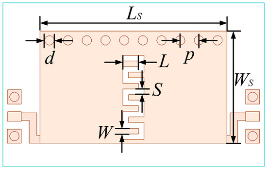
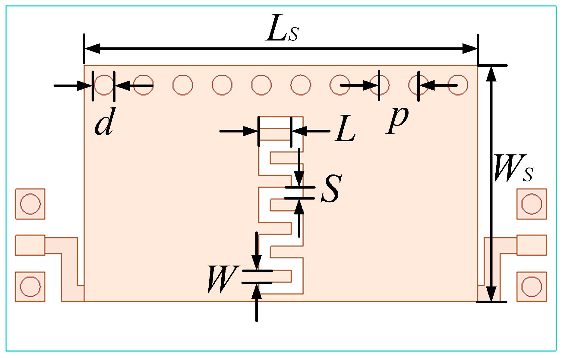
Figure 1 shows the schematic of an HMSIW filter loaded with a single IDC. This structure is realized by etching an IDC on the top metal layer of the HMSIW transmission line. The IDC has a bandstop characteristic, which, combined with the highpass characteristic of the HMSIW transmission line, can construct a wideband bandpass transmission characteristic. The primary structural characteristics of the interdigital capacitor are defined by four key geometric parameters: finger width (W), finger spacing (S), finger length (L), and the number of fingers (n). The finger width (W) refers to the width of the metallic fingers that compose the interdigital arrangement, directly affecting both the current-carrying capacity and the parasitic inductance associated with the fingers. Finger spacing (S) denotes the distance between adjacent metallic fingers and serves as a crucial factor in controlling the strength of the electric field coupling; a reduction in spacing results in an increase in the equivalent capacitance. Finger length (L) corresponds to the effective extension of the metallic fingers, determining the coupling area of the interdigital capacitor; longer fingers yield a larger coupling area and, consequently, a higher equivalent capacitance. Lastly, the number of fingers (n) represents the total count of metallic fingers in the interdigital structure, with an increase in this number significantly augmenting the overall capacitance. By precisely controlling these four parameters, the IDC can be flexibly adapted to different circuit capacitance and parasitic characteristic requirements. When the finger width W equals the finger spacing S, the maximum capacitance density can be obtained, and the capacitance value can be estimated by Equation (1) [20], where is the relative permittivity of the substrate, and L is the finger length of the IDC in micrometers (μm).
Figure 1.
HMSIW filter loaded with single IDC.
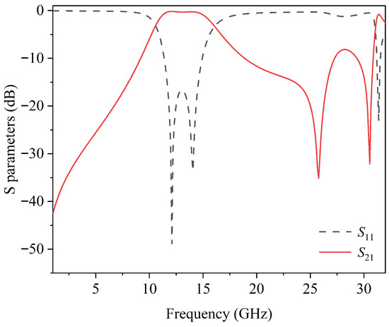
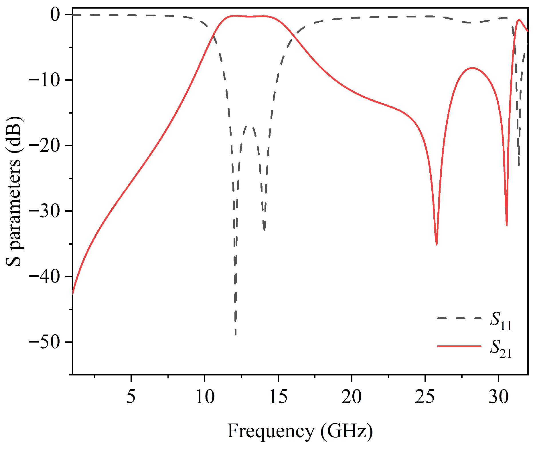
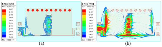
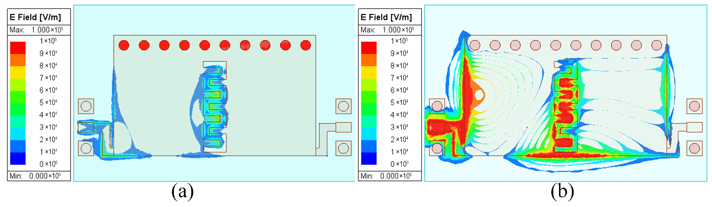
This paper first investigates the transmission characteristics of the IDC-loaded HMSIW using a single-layer alumina ceramic substrate with a thickness of 0.254 mm and a relative permittivity of 9.9. The HMSIW structure features a width () of 2.4 mm and a length of 4 mm along the transmission direction. The metallized via holes possess a diameter of 0.2 mm and are arranged with a pitch (p) of 0.4 mm. The interdigital capacitor integrated into the design exhibits finger widths (W) and finger spacings of 0.12 mm, with each finger having a length (L) of 0.33 mm. Electromagnetic simulations of the IDC-loaded HMSIW filter were conducted using high-frequency simulation software, and the corresponding results are presented in Figure 2. From the simulation results, the cutoff frequency of the HMSIW is 11 GHz. Additionally, two transmission zeros appear in the passband range of the HMSIW at 25.4 GHz and 30.5 GHz. These transmission zeros can create stopbands within the HMSIW passband, thereby achieving a wideband bandpass filtering response. The transmission zero observed at 25.4 GHz is attributed to the loaded interdigital capacitor, whereas the transmission zero occurring at 30.5 GHz results from the self-resonance phenomenon inherent to the half-mode substrate-integrated waveguide resonator. To elucidate the formation mechanism of the transmission zeros, a simulation analysis of the electric field distribution is conducted on the single-IDC-loaded HMSIW. Figure 3a illustrates the electric field distribution at the transmission zero frequency of 25.4 GHz. At this frequency, the electric field is entirely obstructed at the IDC, preventing transmission to the opposite port and thereby generating a transmission zero. This observation indicates that the transmission zero is primarily governed by the IDC. Figure 3b illustrates the electric field distribution at the transmission zero occurring at 30.5 GHz. It is evident that the interdigital capacitor does not obstruct the conduction of the electric field. However, at this specific frequency, the electric field resonates within the cavity formed by the half-mode substrate-integrated waveguide, preventing its propagation to the opposite port. Consequently, this transmission zero is attributed to the resonance of the HMSIW cavity.
Figure 2.
Response of HMSIW filter loaded with single IDC.
Figure 3.
Distribution of the electric field in the HMSIW filter incorporating a single IDC at transmission zero frequencies. (a) Electric field distribution at the transmission zero of 25.4 GHz. (b) Electric field distribution at the transmission zero of 30.5 GHz.
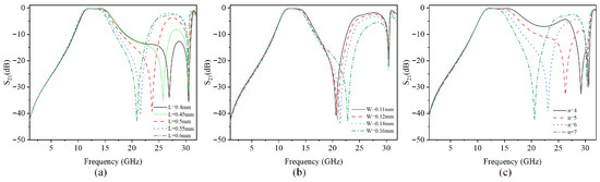
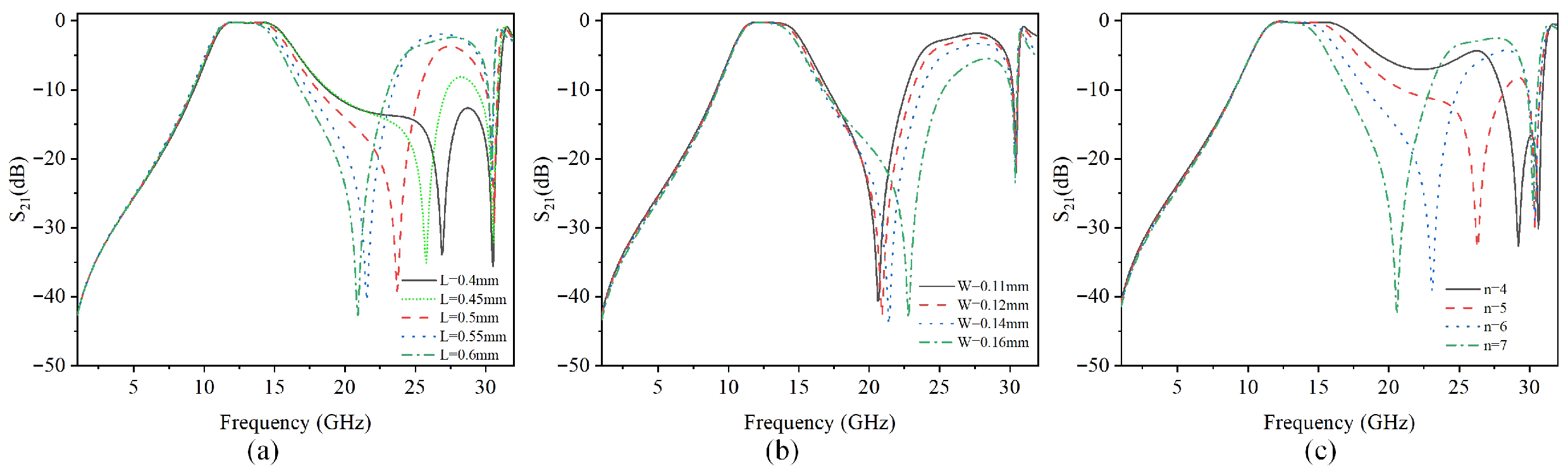
The impact of the structural parameters of the IDC on transmission zeros is examined in the following section. Figure 4a illustrates the effect of the IDC finger length (L) on the transmission zeros. Based on the preceding analysis, the HMSIW filter incorporating a single IDC exhibits two transmission zeros: the lower transmission zero arises from the IDC, while the higher transmission zero results from the resonant behavior of the HMSIW resonator. An increase in the IDC finger length (L) causes the lower transmission zero to shift toward lower frequencies. This phenomenon can be attributed to the fact that a longer finger length (L) increases the capacitance of the IDC, consequently lowering the frequency of the corresponding transmission zero. The transmission zero at the higher frequency of 30.5 GHz is not affected by the IDC finger length L, because this transmission zero originates from the resonance of the HMSIW resonator, and increasing the finger length L does not change the inherent characteristics of the HMSIW resonator. Figure 4b illustrates the effect of the interdigitated capacitor finger width, denoted as W, on the transmission zeros, with the finger spacing S maintained equal to W throughout the experiment. An increase in the finger width W results in a progressive shift of the lower transmission zero toward higher frequency values. From Equation (1), when the IDC finger width W equals the finger spacing S, the capacitance value of the IDC is only related to the finger length L; therefore, the increase in finger width W does not change the capacitance value of the IDC. The upward shift of the lower transmission zero frequency with increasing finger width (W) can be attributed to the reduction in parasitic inductance of the interdigital capacitor resulting from the wider fingers. This decrease in parasitic inductance leads to the observed frequency shift toward higher values. Furthermore, the higher transmission zero at 30.5 GHz remains unaffected by variations in finger width, which corroborates that this transmission zero originates from the resonance phenomenon within the HMSIW cavity. Figure 4c depicts the influence of the number of IDC fingers (n) on the transmission zeros. The simulation results indicate that an increase in the number of fingers leads to a higher equivalent capacitance of the IDC, thereby causing the transmission zero governed by the IDC to shift toward a lower frequency. This observation aligns with the theoretical predictions.
Figure 4.
Effect of interdigital capacitor structural parameters on transmission zeros. (a) Impact of varying IDC finger lengths (L) on the transmission zeros. (b) Impact of varying IDC finger widths (W) on the transmission zero. (c) Impact of varying number of IDC fingers (n) on the transmission zero.
The equivalent LC circuit of the HMSIW filter loaded with a single IDC is shown in Figure 5. In this circuit, represents the capacitance value of the loaded IDC, is the parasitic inductance of the IDC, is the MIM capacitance formed between the upper and lower plates of the HMSIW, is the inductance formed by the HMSIW metallized via holes, and is the parasitic inductance of the HMSIW transmission line. The capacitance value of can be derived using the IDC capacitance calculation in Formula (1). Meanwhile, the capacitance value of is influenced by the geometric dimensions of the upper and lower metal plates of the HMSIW, as well as the properties and thickness of the substrate material. When the parameters of the single interdigital capacitor depicted in Figure 1 are defined as follows: finger length , finger width , finger spacing , and number of fingers , the equivalent circuit capacitance can be derived using the IDC calculation formula. The capacitance is determined by Equation (2), where represents the relative permittivity of the substrate, denotes the vacuum permittivity (), S corresponds to the area of the capacitor plates, and d is the thickness of the dielectric substrate. By applying the dimensions of the HMSIW plates, excluding the region etched by the IDC, into the equation, the value of is calculated to be . The remaining parameters of the equivalent LC circuit are specified as follows: , , and . Figure 6 presents a comparison between the results obtained from electromagnetic simulations and those derived from the equivalent LC circuit model of the HMSIW filter incorporating a single IDC. Given that the transmission zero observed at the higher frequency of 30.5 GHz is unrelated to the IDC, the equivalent circuit analysis focuses exclusively on the transmission zero occurring at the lower frequency. Electromagnetic (EM) simulations and equivalent LC circuit simulations of the HMSIW filter incorporating a single IDC demonstrate strong concordance within the passband and the lower stopband regions. However, discrepancies arise in the attenuation levels observed in the higher stopband between the EM and LC circuit simulation results. These deviations primarily stem from the idealized representation of lumped elements in the LC model, which fails to account for substrate and conductor losses, as well as parasitic effects inherent to the physical structure. Furthermore, the EM simulation reveals an additional transmission zero at 30.5 GHz, attributed to the self-resonance phenomenon of the HMSIW resonant cavity, which further contributes to the attenuation differences observed in the high stopband between the two simulation approaches.
Figure 5.
Equivalent LC circuit model of HMSIW filter loaded with single IDC.
Figure 6.
Comparison between electromagnetic simulation and equivalent LC circuit simulation of HMSIW filter loaded with single IDC.
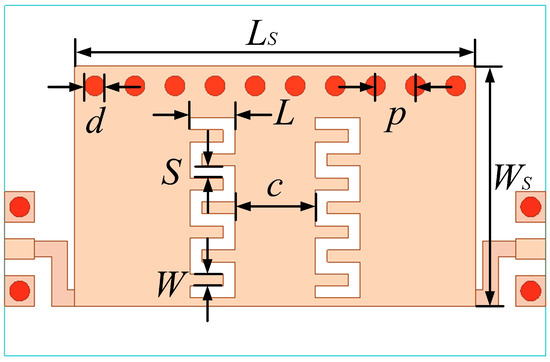
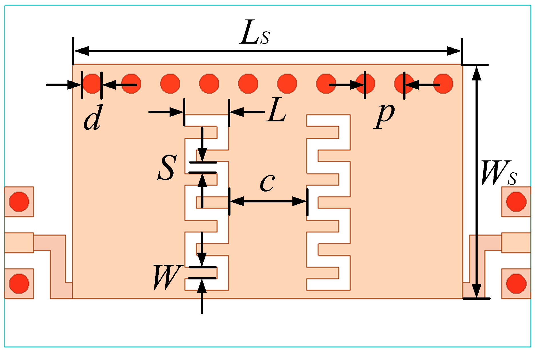
To enhance the stopband bandwidth and achieve greater stopband attenuation, thereby overcoming the limitation of narrow stopband width inherent in single-resonator bandstop filters, the following analysis explores a dual-resonator coupling configuration utilizing interdigital capacitors. The presented configuration incorporates two interdigital capacitor bandstop resonators, possessing identical geometrical parameters, etched onto a half-mode substrate-integrated waveguide transmission line. By varying the spacing between these resonators, the coupling strength can be controlled, thereby facilitating an effective extension of the stopband. Figure 7 illustrates the schematic diagram of the HMSIW filter integrated with the dual-IDC resonators. In this dual-resonator coupling arrangement, the HMSIW transmission line serves as the signal propagation medium, while the principal functional components consist of the two IDC bandstop resonators. The IDC adopts a symmetrical design, with its metal fingers uniformly arranged along the HMSIW transmission line direction. This design facilitates a pronounced concentration of the electric field, thereby establishing a basis for energy coupling between the two resonators. The spacing between resonators, denoted as c, serves as a critical parameter for modulating the coupling strength. As previously analyzed, a structure incorporating a single IDC can be modeled as an equivalent parallel LC resonator, where represents the capacitance of the IDC and corresponds to its parasitic inductance. The intrinsic resonant frequency of this configuration is governed by the parallel LC resonance properties, with the precise resonant frequency expressed by Equation (3).
Figure 7.
HMSIW filter loaded with dual IDCs.
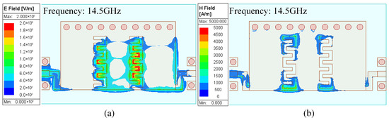
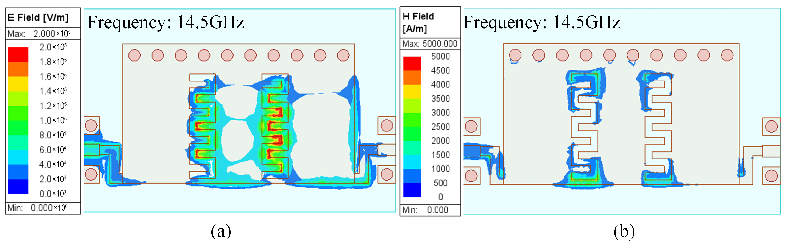
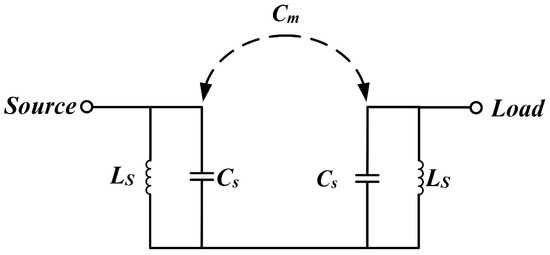
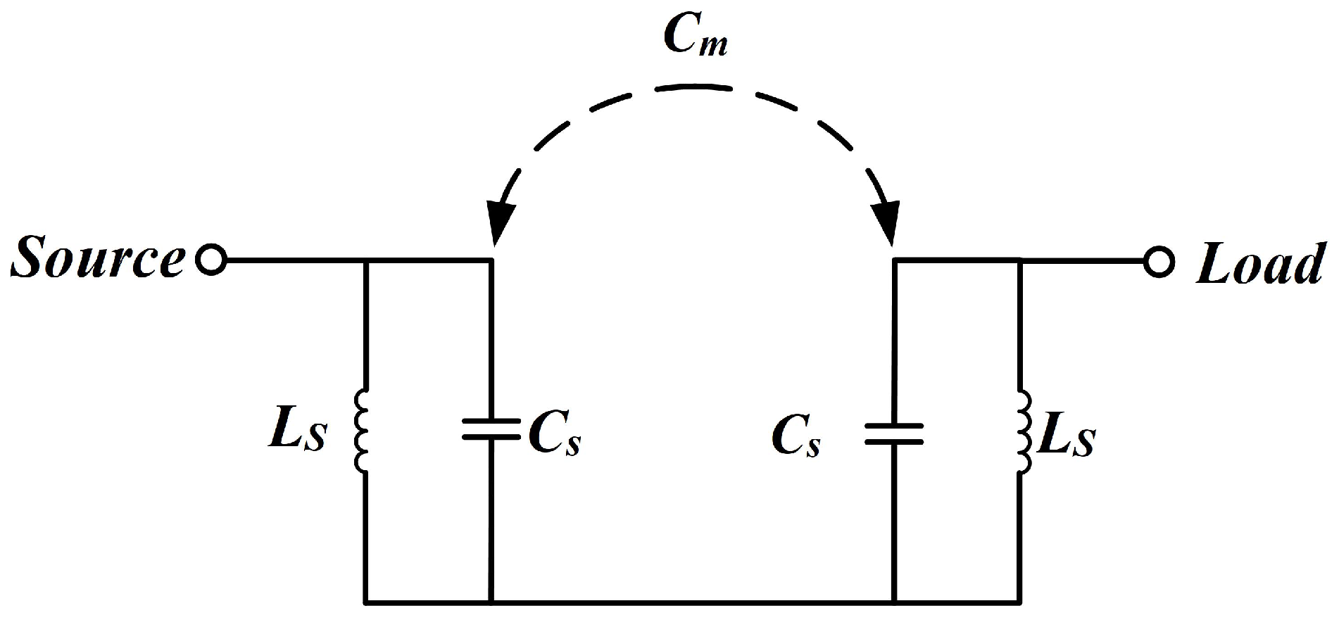
To elucidate the coupling mechanism between the dual interdigital capacitors, an analysis of the electromagnetic field distribution was conducted through simulation on the two IDCs. Figure 8 depicts the distribution of the electromagnetic field within the HMSIW filter incorporating dual IDCs at the frequency of 14.5 GHz. The simulation results indicate that the coupling between the two IDCs predominantly occurs via the electric field, thereby identifying electric coupling as the principal coupling mechanism in the dual-IDC-loaded configuration. Given that the research primarily concentrates on the location of transmission zeros, the electric coupling between the two interdigital capacitors within the narrowband region surrounding these transmission zeros can be effectively modeled by a coupling capacitance, denoted as . The corresponding equivalent LC circuit representing the electric coupling between the two IDCs is illustrated in Figure 9. In this circuit, denotes the parasitic inductance associated with a single IDC, represents the capacitance of an individual IDC, and signifies the coupling capacitance that characterizes the electric interaction between the two IDCs.
Figure 8.
Electromagnetic field distribution of HMSIW filter loaded with dual IDCs. (a) Electric field distribution. (b) Magnetic field distribution.
Figure 9.
Equivalent LC circuit of electric coupling between dual IDCs.
Owing to the complete symmetry of the parameters of the two resonators, the coupling interaction induces a splitting of the originally degenerate intrinsic resonant modes, resulting in the formation of two distinct transmission zeros corresponding to the lower frequency and the higher frequency , respectively. The quantitative relationships between these transmission zeros and the equivalent circuit parameters , , and are expressed by Equations (4) and (5). These equations elucidate the intrinsic connection between the transmission zeros and the equivalent circuit parameters: the mutual capacitance enables precise modulation of the transmission zero positions by altering the effective capacitance of the resonant units. Specifically, for the lower transmission zero , the mutual capacitance combines additively with the interdigital capacitor , thereby increasing the equivalent capacitance () and consequently lowering the resonant frequency. Conversely, for the higher transmission zero , the mutual capacitance exerts a subtractive effect, decreasing the equivalent capacitance () and thus elevating the resonant frequency. Furthermore, the capacitive coupling coefficient between the two resonators is defined as .
Since the mutual capacitance is much smaller than the IDC capacitance , the relationship between the lower transmission zero , the higher transmission zero fm, and the single-resonator inherent frequency can be approximately related by Equation (6). This expression explicitly demonstrates that the product of the two transmission zero frequencies in the dual-resonator coupling system is equal to the square of the single-resonator inherent frequency, a relationship that remains invariant with respect to the coupling strength. The stopband width is defined as the difference between and (), and its magnitude is directly influenced by the value of the mutual capacitance . Specifically, an increase in results in a more pronounced splitting of the two transmission zeros, thereby broadening the corresponding stopband width.
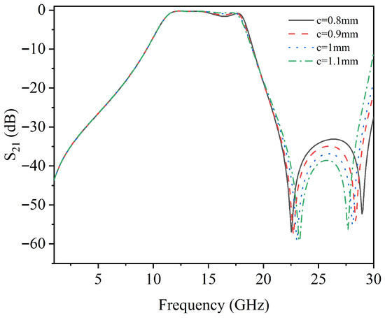
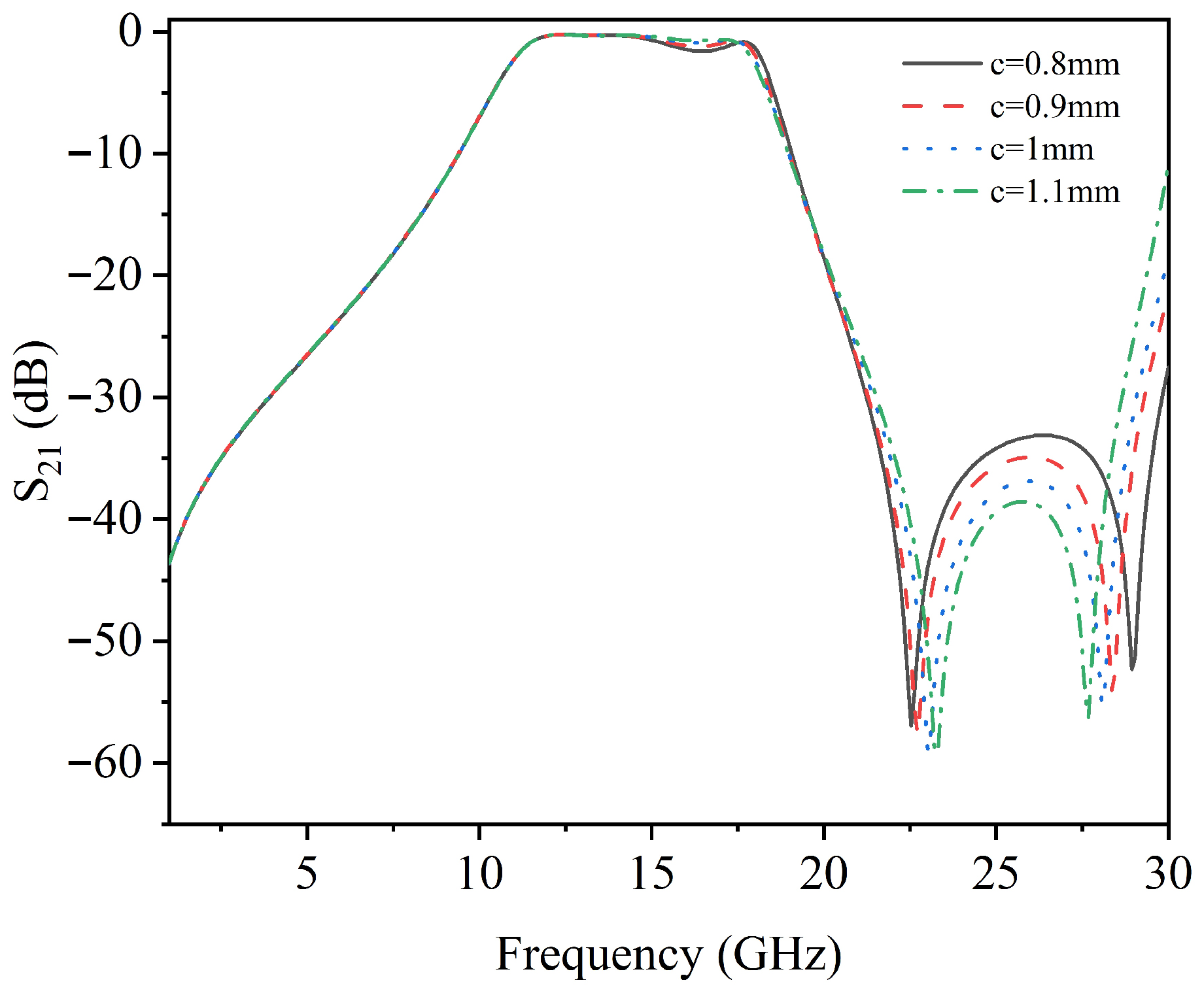
Full-wave simulations of the dual-IDC resonator coupling structure with varying coupling spacings were conducted utilizing the high-frequency electromagnetic simulation software HFSS. The transmission zero characteristics were subsequently analyzed through the extraction of S parameters. Figure 10 shows the transmission characteristics of the HMSIW filter loaded with dual IDCs under different coupling spacings c from full-wave simulation. In this full-wave simulation model, the parameters of an individual interdigital capacitor are defined as follows: the finger length (L) is 0.33 mm, the finger width (W) and the finger spacing are both 0.12 mm, and the number of fingers (n) is set to seven. The transmission zero produced solely by a single IDC is observed at a frequency of 25.4 GHz. Table 1 shows the distribution of transmission zeros for the HMSIW filter loaded with dual IDCs under different coupling spacings c. From the data in the table, it can be seen that under different coupling spacings c, the product of the two split transmission zeros and fm is approximately equal to the square of the single-IDC transmission zero position , which is consistent with the theoretical criterion derived above. At the same time, as the coupling spacing c decreases, the coupling strength between the two resonators gradually increases, causing the difference between the two transmission zeros fm and to increase, thereby effectively extending the stopband width of the filter.
Figure 10.
Effect of varying the spacing between dual interdigitated capacitors on transmission zeros as determined by full-wave simulation.
Table 1.
Distribution of transmission zeros under different spacings c between dual IDCs.
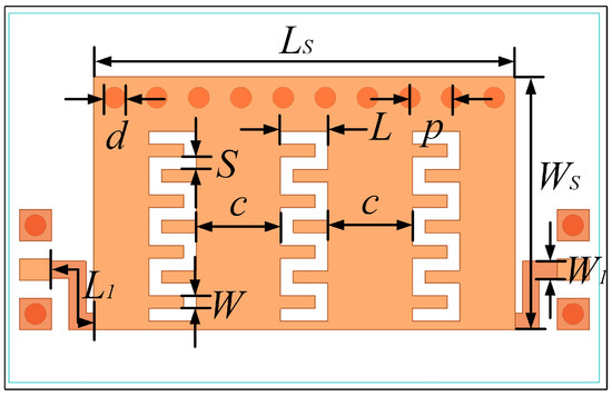
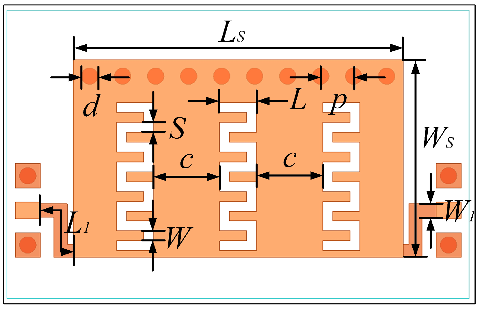
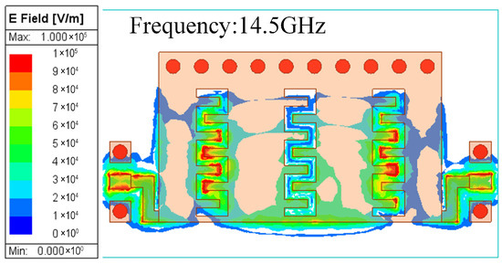
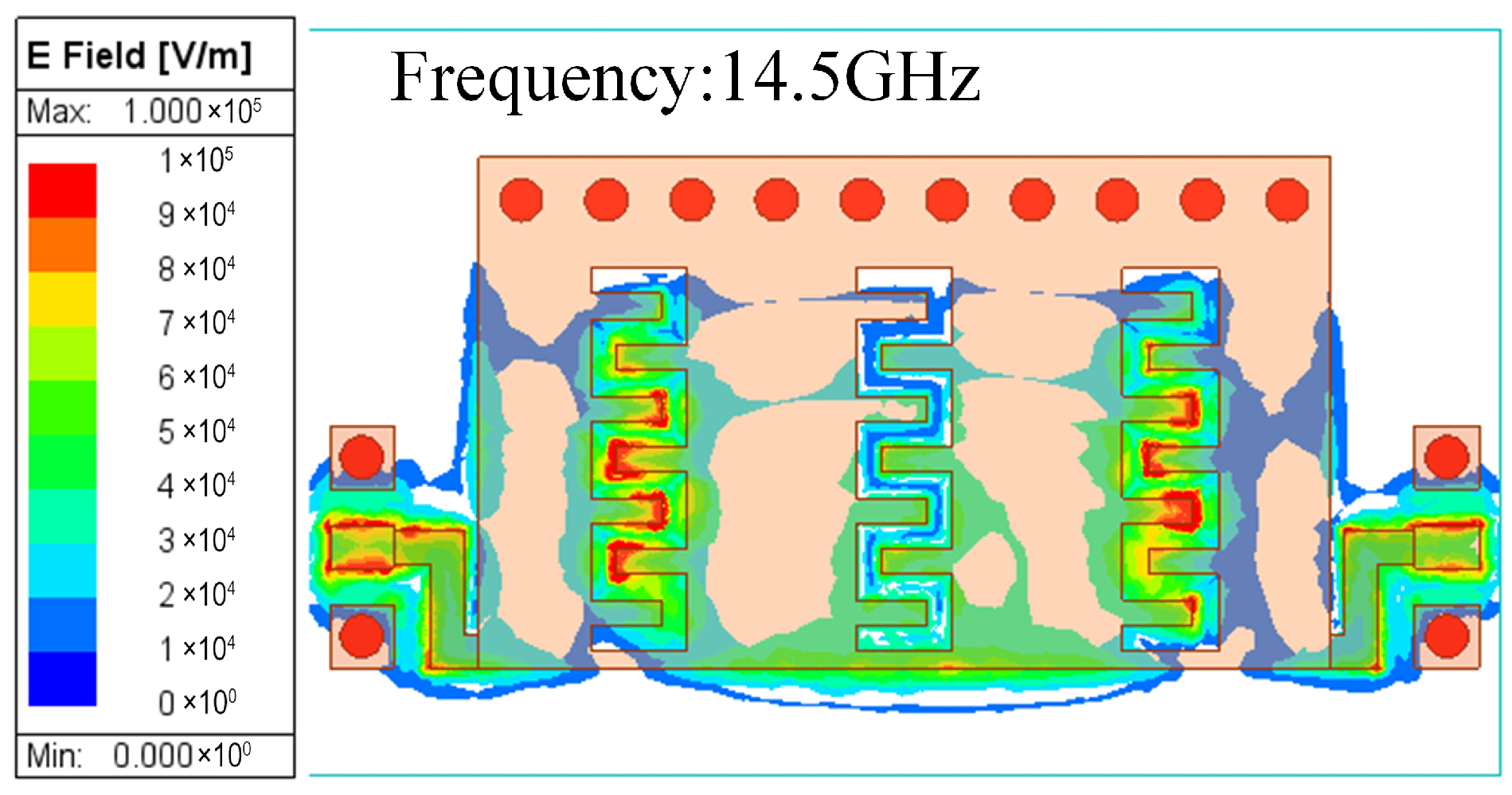
To further improve the stopband bandwidth and attenuation performance of the IDC-loaded configuration, this study builds upon prior investigations of single- and dual-IDC loading by introducing a HMSIW filter incorporating triple-IDC elements. Figure 11 illustrates the configuration of the wideband half-mode substrate-integrated waveguide filter incorporating three interdigital capacitors. The integration of these three IDCs onto the HMSIW transmission line facilitates the realization of a wide passband without necessitating an increase in the overall filter dimensions. The filter substrate remains based on the HMSIW structure, with the following geometric parameters preserved: a width () of 2.4 mm, a transmission direction length of 4 mm, metallized via holes with a diameter of 0.2 mm, a hole pitch (p) of 0.4 mm, and a compact core dimension of 4 mm × 2.4 mm. The three IDCs are evenly distributed along the axis of the HMSIW transmission line, maintaining an inter-capacitor spacing (c) of 0.8 mm, consistent with the spacing employed in configurations featuring strongly coupled dual IDCs. The IDC structural parameters are consistent with those previously described, specifically: finger width (W) of 0.12 mm, finger spacing (S) of 0.12 mm—optimized to achieve maximum capacitance density—finger length () of 0.33 mm, and a total of seven fingers (). The bent feeding structure employed in this design prioritizes two principal objectives: the miniaturization of the feeding port and the achievement of impedance matching, with a fixed bending angle of 90°. Through the implementation of a folded feeding path, the physical dimensions of the feeding port are significantly reduced, thereby enhancing compatibility with the overall compact configuration of the capacitance-loaded HMSIW filter. The primary function of this feeding structure is to facilitate efficient impedance matching between the capacitance-loaded HMSIW and the standard port. Theoretically, the feeding line length required for impedance matching corresponds to one-quarter of the wavelength at the filter’s center frequency. However, due to the combined influence of parasitic electromagnetic effects introduced by the 90° bend and the intrinsic electromagnetic coupling between the feeding line and the capacitance-loaded HMSIW, the optimized feeding line length deviates from the ideal quarter-wavelength during high-frequency electromagnetic simulation and optimization. Consequently, this design treats the feeding line’s width and length as critical optimization parameters, which are finely tuned through iterative high-frequency electromagnetic simulations. This approach effectively mitigates impedance discontinuities caused by structural bending and parasitic phenomena, ensures that the filter’s input and output impedances maintain good matching with across the entire operating passband, and prevents degradation in insertion loss and return loss resulting from impedance mismatches at the feeding port. The detailed structural parameters of the filter are listed in Table 2. Figure 12 shows the coupling electric field distribution of the wideband miniaturized HMSIW filter loaded with IDCs at the central frequency of 14.5 GHz. Similar to the dual-IDC coupling mechanism discussed above, the IDCs in the HMSIW filter loaded with triple IDCs still dominate in electric coupling.
Figure 11.
Schematic of wideband miniaturized HMSIW filter loaded with three IDCs.
Table 2.
Structural parameters of wideband miniaturized HMSIW filter loaded with IDCs (unit: mm).
Figure 12.
Coupling electric field distribution of wideband miniaturized HMSIW filter loaded with three IDCs.
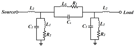
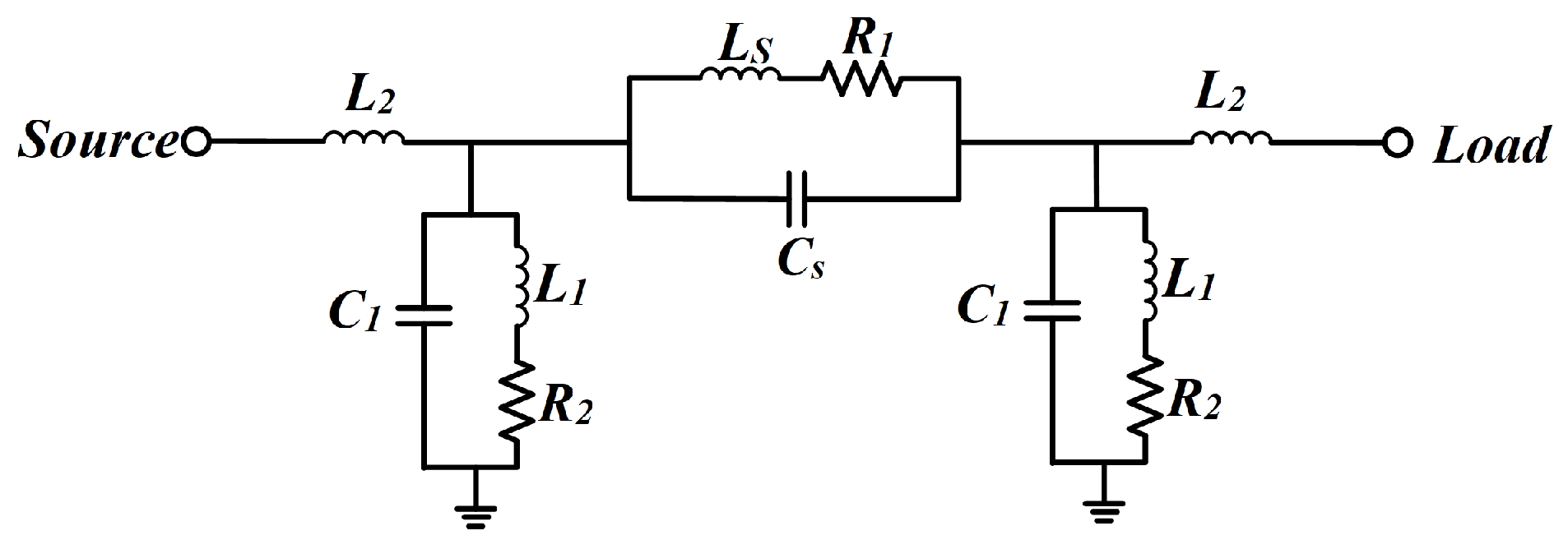
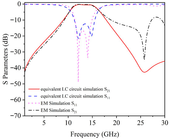
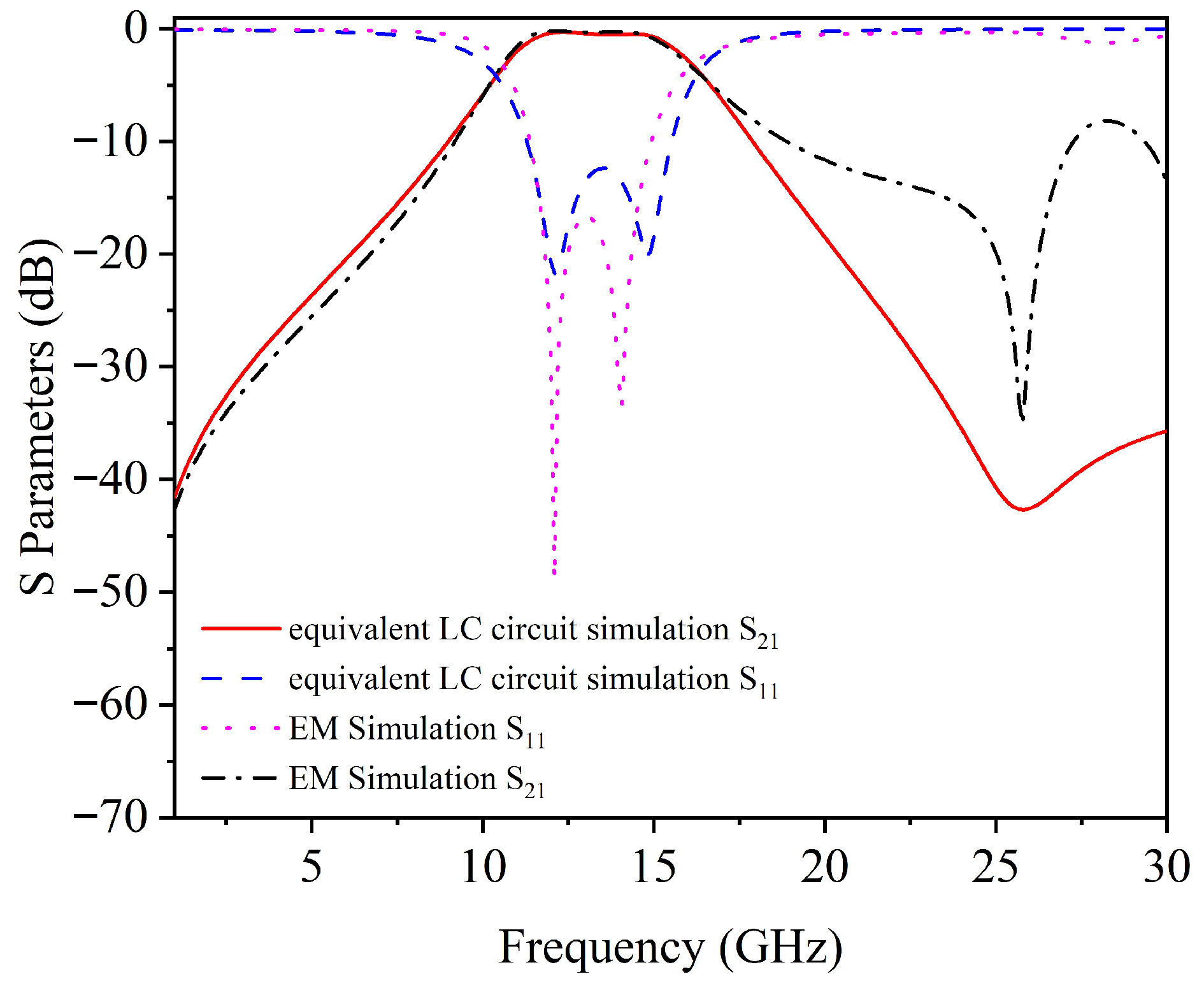
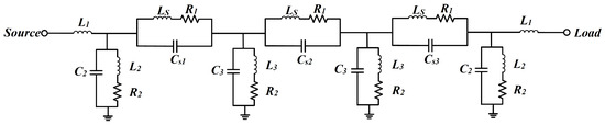
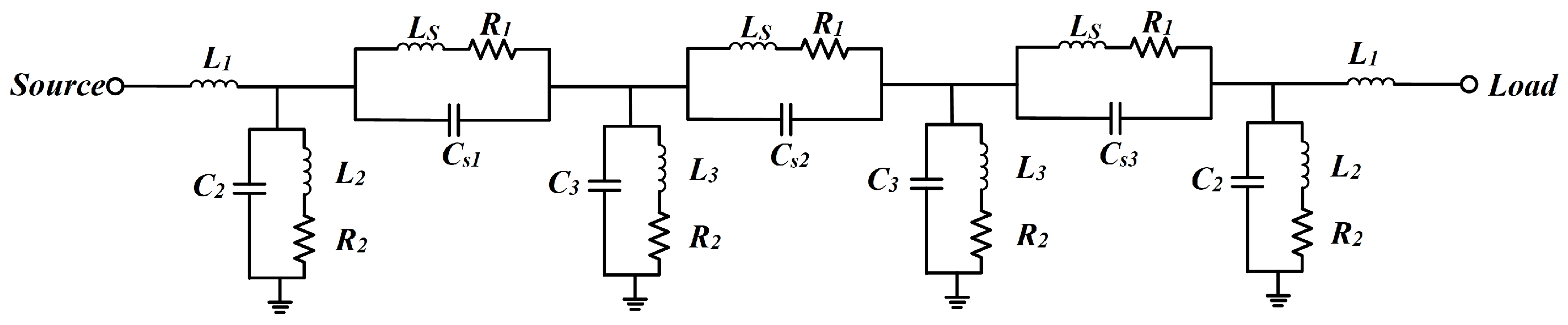
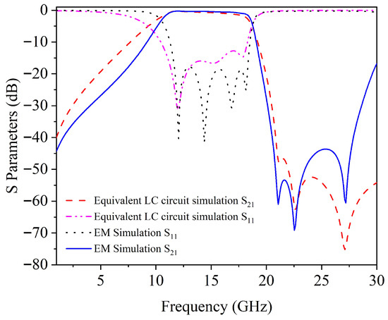
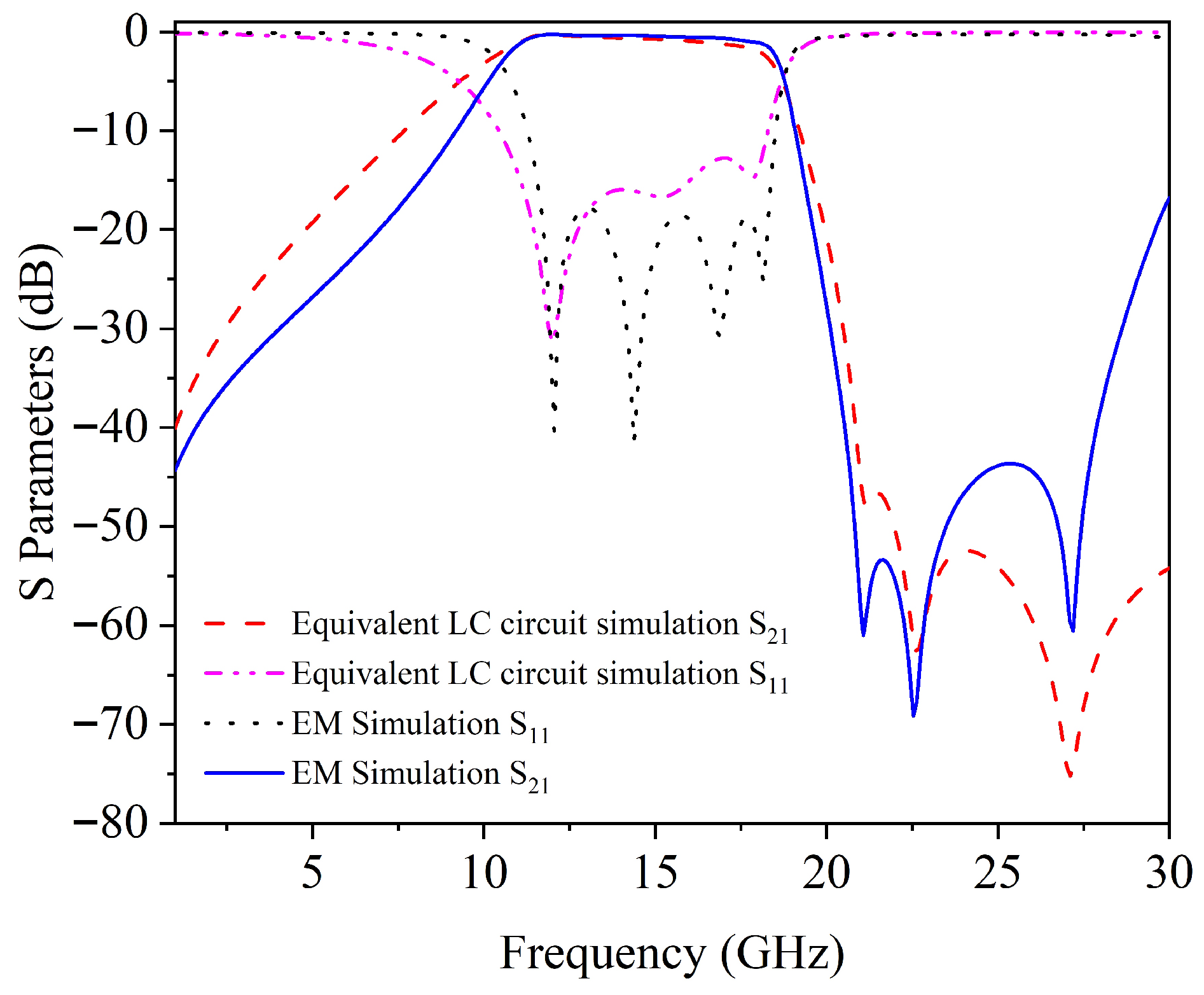
To further validate the theoretical analysis and elucidate the electromagnetic coupling mechanism of the proposed third-order IDC-loaded HMSIW filter, an equivalent LC circuit model of the filter was developed, as illustrated in Figure 13. This model facilitates an accurate physical representation of the fundamental electromagnetic behaviors inherent to the filter. Initially, three sets of parallel LC resonant units, connected in series along the main transmission path, were employed to characterize the bandstop properties of the three IDC loading elements. The inductance parameter for each unit was uniformly assigned as to account for the parasitic inductance associated with the metal fingers of the IDCs. Due to the electrical coupling between IDC units, the equivalent capacitance parameters exhibited a non-uniform distribution, with values of , , and , respectively. This capacitance differentiation constitutes the principal physical mechanism enabling the filter to regulate multiple transmission zeros. Additionally, the resistor was introduced to model the intrinsic loss characteristics of the IDCs. Subsequently, four sets of parallel LC resonant branches, symmetrically arranged around the main transmission path, were utilized to represent the inherent resonant features of the HMSIW main cavity. Specifically, the pairs with and with form the fundamental resonant units of the HMSIW, which critically determine the passband center frequency of the filter. Their respective values were assigned as , , , and . The resistor was incorporated to equivalently represent conductor, dielectric, and radiation losses within the HMSIW cavity, thereby ensuring that the model’s quality factor aligns with that of the actual device. In addition, denotes the coupling between the feeding port and the filter. Figure 14 presents a comparative analysis of the S parameters obtained from this equivalent circuit model and full-wave EM simulations. The results demonstrate a high degree of concordance between the transmission characteristics of the equivalent circuit and the EM simulations, with exact alignment of transmission zero positions within the stopband and closely matching attenuation trends. Collectively, these findings substantiate that the proposed equivalent LC circuit model accurately captures the bandstop behavior induced by third-order IDC coupling as well as the resonant characteristics of the HMSIW cavity, thereby providing robust circuit-level validation for the theoretical framework presented herein.
Figure 13.
Equivalent LC circuit of HMSIW filter loaded with three IDCs.
Figure 14.
Comparison of simulation results between equivalent LC circuit and EM for HMSIW filter loaded with three IDCs.
The results indicate that the filter exhibits a 1 dB passband spanning from 11 GHz to 18 GHz, corresponding to a fractional bandwidth of 48.3%. Regarding passband performance, the filter achieves a minimum in-band insertion loss of merely 0.28 dB, alongside an in-band return loss below −17.8 dB, thereby demonstrating superior passband transmission characteristics. Concerning out-of-band suppression, the filter generates transmission zeros at frequencies of 21.1 GHz, 22.5 GHz, and 27.2 GHz. These transmission zeros significantly enhance the filter’s out-of-band rejection and effectively broaden the stopband, extending the suppression level of −40 dB up to 27.9 GHz. In terms of physical dimensions, the core size of this wideband filter measures only 4 mm by 2.4 mm, which corresponds to in guided wavelength units, thereby clearly illustrating the advantages of the miniaturized design.
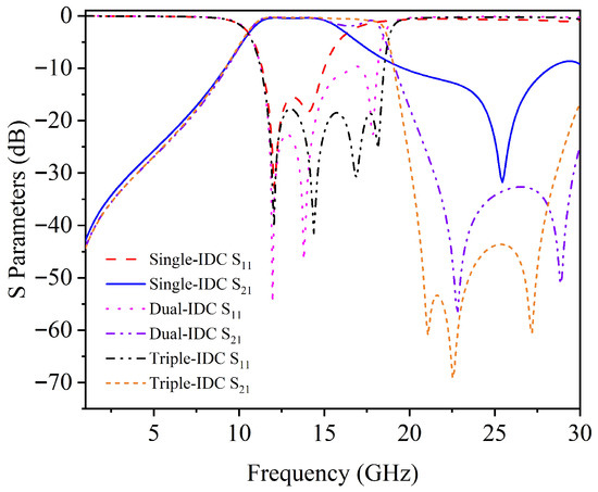
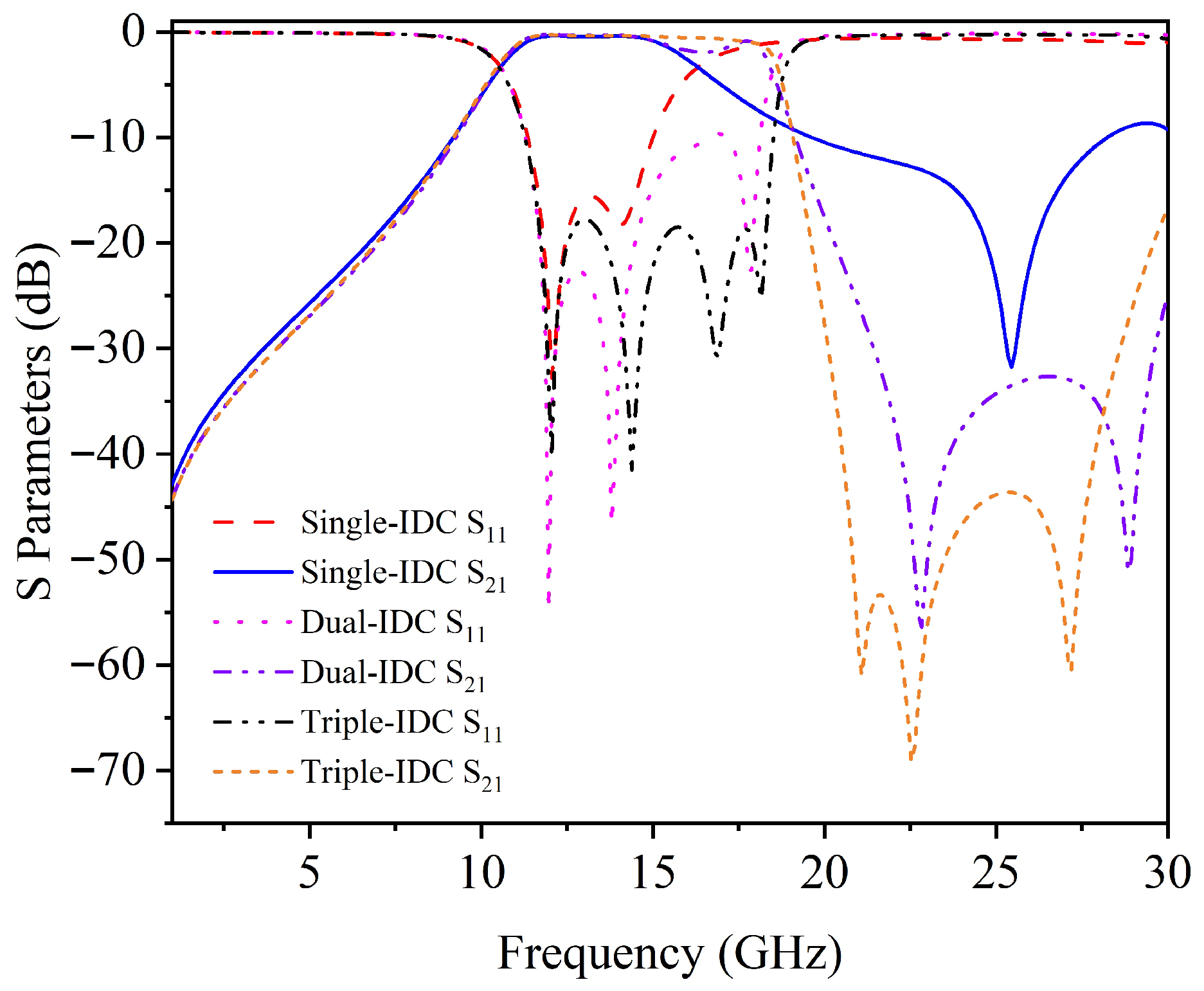
To examine the influence of the number of IDCs on the filtering performance of HMSIW filters, a comparative study was conducted involving filters loaded with one, two, and three IDCs. The differences in their performance and the distribution of transmission zeros are illustrated in Figure 15. The findings reveal a pronounced positive correlation between the quantity of loaded IDCs and the number of transmission zeros present in the filter’s stopband. Specifically, the HMSIW filter with a single IDC exhibits only one transmission zero at 25.4 GHz; the dual-IDC configuration produces two distinct transmission zeros at 22.5 GHz and 29.0 GHz, attributed to resonator coupling; the triple-IDC arrangement generates three transmission zeros at 21.1 GHz, 22.5 GHz, and 27.2 GHz. The increase in transmission zeros substantially enhances the filter’s ability to suppress undesired signals within the stopband, thereby significantly improving its frequency selectivity. Conversely, the single-IDC design, limited by the presence of only one transmission zero, fails to establish an effective and broad stopband, rendering it inadequate for wideband bandpass filtering requirements. In contrast, the dual-IDC and triple-IDC configurations leverage the combined effect of multiple transmission zeros to create an effective stopband spanning a wide frequency range, thereby facilitating wideband filtering performance.
Figure 15.
Comparison of simulation results for HMSIW filters loaded with single IDC, dual IDCs and triple IDCs.
2.2. Modified HMSIW Transmission Line Analysis and Its Filter Application
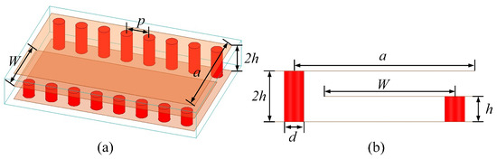
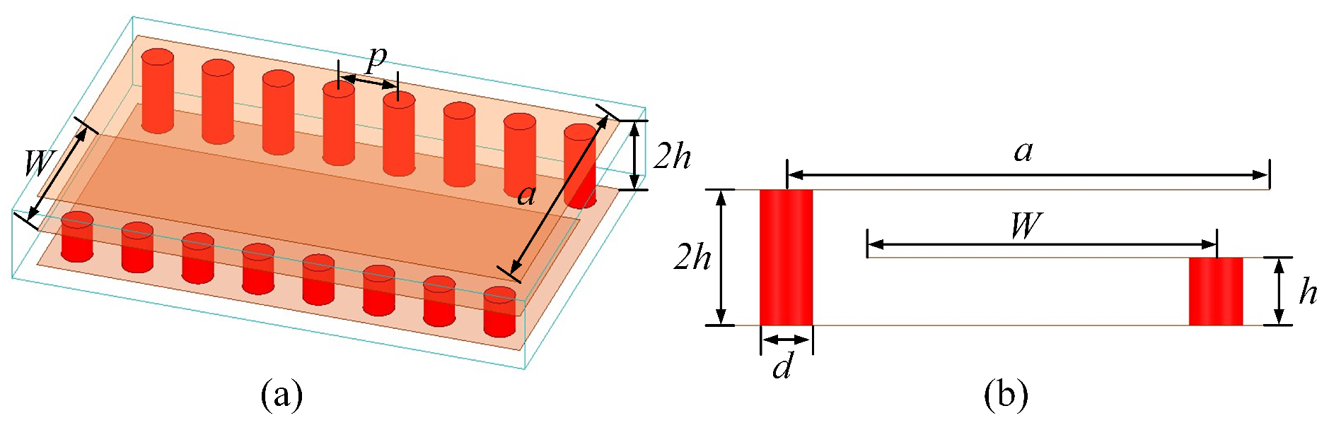
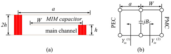
To achieve a further reduction in the size of the IDC-loaded wideband HMSIW filter, an effective and practical approach involves decreasing the transverse width of the HMSIW transmission line while maintaining its cutoff frequency. Figure 16 shows the schematic of a modified HMSIW transmission line loaded with a MIM capacitor, fabricated via double-layer ceramic thin-film technology. The MIM capacitor is integrated at the equivalent magnetic wall on the cross-section of the HMSIW. The fundamental waveguide width, denoted as a, is characterized as the distance between the metallic via-fence electric wall and the open boundary. The MIM capacitor is integrated at the intrinsic open boundary of the HMSIW. Specifically, its upper plate, possessing a transverse width W, extends into the HMSIW and establishes a vertical capacitor configuration with the top metal layer, separated by a plate spacing h. Meanwhile, the lower plate is electrically connected to the bottom ground plane via metallized vias. The incorporation of a capacitor-loaded configuration effectively lowers the cutoff frequency of the structure while maintaining minimal transmission loss.
Figure 16.
Schematic of modified HMSIW transmission line structure. (a) 3D view. (b) Cross-section view.
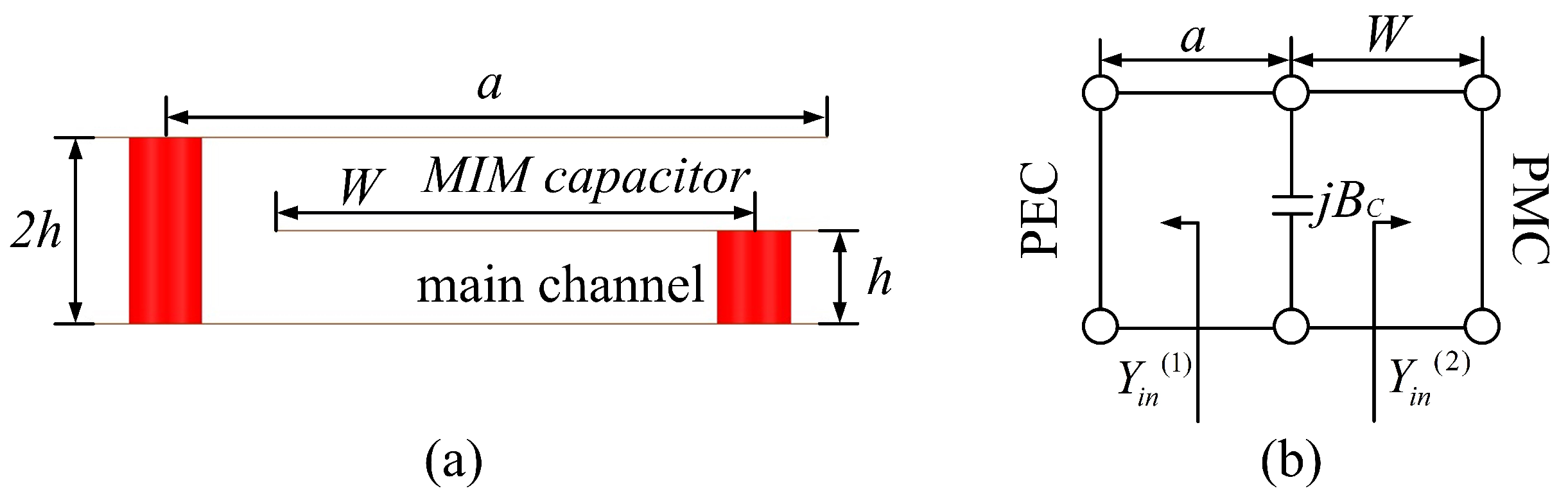
In this study, the transverse resonance method is utilized to investigate the cutoff characteristics of the capacitor-loaded HMSIW structure. The fundamental concept underlying this approach involves selecting a reference plane along the transverse (x) direction of the waveguide and imposing the condition that the sum of the input admittances observed from both the left and right sides of this reference plane equals zero. This condition facilitates the derivation of the eigenvalue equation corresponding to the mode under consideration. Specifically, for the capacitor-loaded HMSIW structure examined here, the reference plane is positioned at the location of the capacitor loading, defined as in the transverse direction of the waveguide. Figure 17 illustrates the cross-sectional view of this capacitor-loaded HMSIW transmission line configuration and its associated transverse equivalent circuit model.
Figure 17.
Cross-section view and transverse equivalent circuit of capacitor-loaded HMSIW transmission line. (a) Cross-section view. (b) Transverse equivalent circuit.
The transverse equivalent circuit can be represented as a transmission line characterized by an admittance , a length denoted by a, and terminated by a short circuit when observed from the equivalent electric wall. The input admittance of this configuration is given by:
where is the characteristic admittance of the corresponding transmission line, a is the width of the HMSIW, and is the transverse propagation constant. Looking from the reference plane toward the capacitor plate region is a transmission line with characteristic admittance , length W, and open-circuited termination, with input admittance:
where W is the width of the loaded MIM capacitor plate. In addition, a shunt-lumped capacitor is connected at the reference plane in the transverse equivalent circuit diagram to characterize the loading effect of the MIM capacitor. To correctly reflect the physical fact that the cutoff frequency is an eigenattribute of the waveguide transverse mode (independent of the length in the longitudinal transmission direction), this shunt element should be the susceptance introduced by the unit-length capacitance. The unit-length capacitance value of the MIM capacitor is:
The susceptance normalized to unit length is given by:
The relationship between the transverse propagation constant and the transverse characteristic admittance is determined by the following equation:
Thus, the transverse resonance equation is established:
Deriving the fundamental equation for the transverse propagation constant :
At the cutoff frequency , the longitudinal propagation constant = 0; hence,
Based on the above equations, the equation about the cutoff frequency can be obtained:
where c is the speed of light in a vacuum, and is the relative permittivity of the substrate.
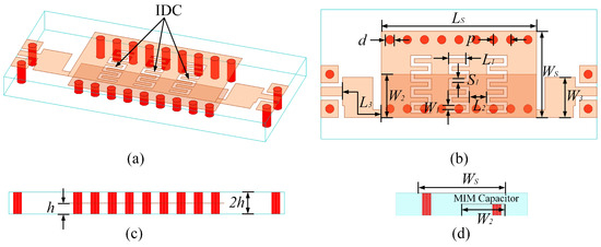
The modified HMSIW introduced in this study and the folded half-mode substrate-integrated waveguide (FHMSIW) described in reference [21] both originate from the conventional HMSIW configuration, with waveguide miniaturization as their fundamental design objective. Nonetheless, they exhibit notable differences in terms of application contexts, theoretical analysis approaches, and primary performance targets. The modified HMSIW presented herein is specifically tailored for wideband microwave filtering applications. Employing the transverse resonance method, a comprehensive theoretical derivation and analysis are conducted, resulting in the establishment of a quantitative theoretical model that correlates the cutoff frequency with structural parameters. This model effectively facilitates the dual design objectives of reducing the transverse waveguide dimensions while ensuring wideband, low-loss transmission. Conversely, the FHMSIW is predominantly designed for frequency beam-scanning antenna applications. Prior studies have primarily focused on simulation-based analyses of its dispersion characteristics and slow-wave phenomena, without developing a complete quantitative theoretical model for the cutoff frequency or constructing a systematic framework for parameter optimization. Considering that MIM capacitor-loaded modified HMSIW transmission lines can substantially lower the cutoff frequency, thereby enabling a reduction in the transverse width of HMSIW transmission lines at an equivalent cutoff frequency, this study presents the design and implementation of a compact wideband SIW bandpass filter. This is achieved by etching interdigital capacitor structures onto the modified HMSIW transmission line. Figure 18 illustrates the IDC-loaded wideband bandpass filter based on the modified HMSIW transmission line. The filter is composed of two alumina ceramic substrates, each with a thickness of 0.254 mm, which are stacked via anodic bonding to form a double-layer ceramic structure. Within the filter, MIM capacitor loading is implemented by incorporating a metal plane of width and length in the intermediate layer, effectively reducing the cutoff frequency of the HMSIW transmission line. The introduction of third-order IDCs etched on the top metal layer creates a bandstop region within the passband of the HMSIW transmission line, thereby enabling wideband bandpass filter functionality. The characteristics of this bandstop region depend on the IDC parameters, including finger length (), finger width (), finger spacing (), and the spacing () between adjacent IDCs. Detailed structural dimensions of the IDC-loaded wideband miniaturized filter based on the modified HMSIW transmission line are provided in Table 3.
Figure 18.
Schematic of IDC-loaded wideband miniaturized filter based on MIM capacitor-loaded HMSIW transmission line. (a) 3D view. (b) Top view. (c) Front view. (d) Side view.
Table 3.
Structural dimensions of IDC-loaded wideband filter based on MIM capacitor-loaded HMSIW transmission line (unit: mm).
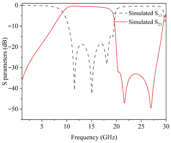
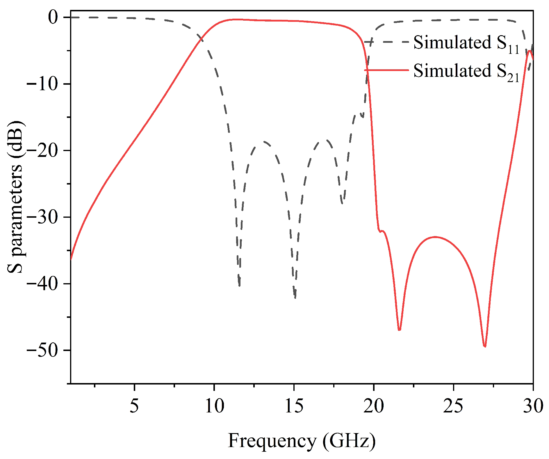
The high-frequency electromagnetic simulation software HFSS was employed to model the aforementioned filter, and the simulation outcomes for the IDC-loaded wideband miniaturized filter, which is based on a MIM capacitor-loaded HMSIW transmission line, are presented in Figure 19. The simulation results indicate that the filter exhibits a 1 dB passband spanning from 10 GHz to 18 GHz, corresponding to a fractional bandwidth of 57.1%. The minimum insertion loss within the passband is simulated at 0.33 dB, while the return loss remains below −18.3 dB, demonstrating superior transmission performance within the operational frequency range. Outside the passband, the filter generates transmission zeros at frequencies of 20.4 GHz, 21.7 GHz, and 27 GHz. These transmission zeros substantially enhance the out-of-band rejection characteristics and effectively widen the stopband, extending the suppression level to −40 dB up to 27.4 GHz. Furthermore, the compact core dimensions of the wideband filter are 3.6 mm × 1.9 mm (), thereby fulfilling the design objective of miniaturization.
Figure 19.
Simulated results of IDC-loaded wideband HMSIW filter with MIM capacitor.
3. Fabrication and Measurement
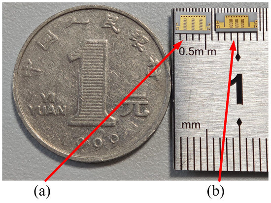
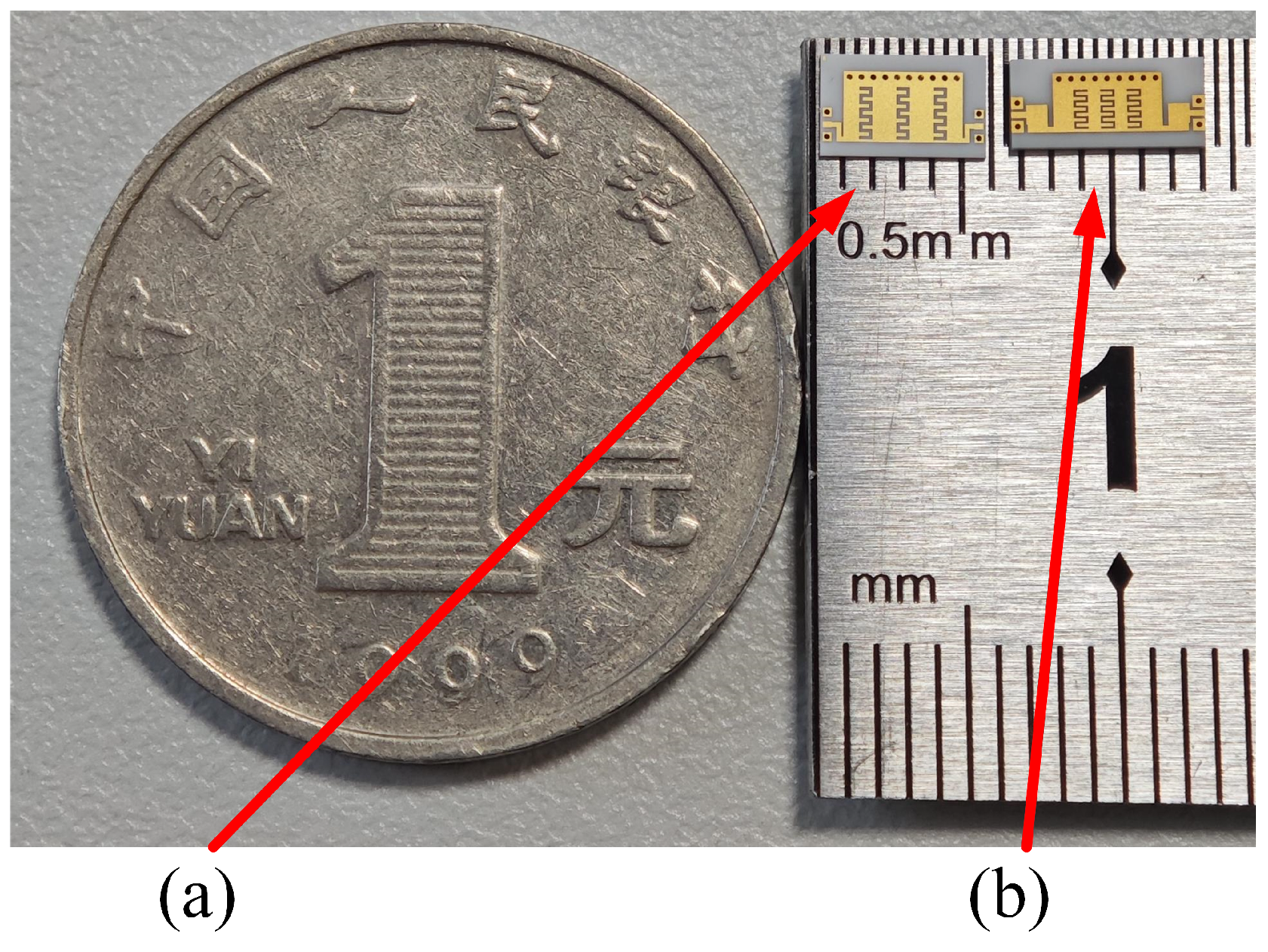
To evaluate the practical performance of the two proposed IDC-loaded wideband HMSIW filters, they were fabricated using their respective manufacturing methods. The IDC-loaded wideband SIW filter, based on the conventional HMSIW transmission line, was produced via single-layer ceramic thin-film technology. In contrast, the IDC-loaded wideband SIW filter employing the modified HMSIW transmission line was fabricated using double-layer ceramic thin-film technology. Both filters were constructed on alumina ceramic substrates with a thickness of 0.254 mm, a relative permittivity of 9.9, and a loss tangent of 0.0002. Figure 20a presents a photograph of the IDC-loaded SIW filter based on the traditional HMSIW transmission line, featuring a compact core dimension of 4 mm × 2.4 mm (). Figure 20b depicts the IDC-loaded SIW filter based on the improved HMSIW transmission line, with an even smaller size of 3.6 mm × 1.9 mm (), thereby illustrating notable miniaturization benefits. The performance of both filters was evaluated using a vector network analyzer in conjunction with a probe station measurement system.
Figure 20.
Images of wideband substrate-integrated waveguide filters incorporating interdigital capacitors. (a) BPF 1. (b) BPF 2.
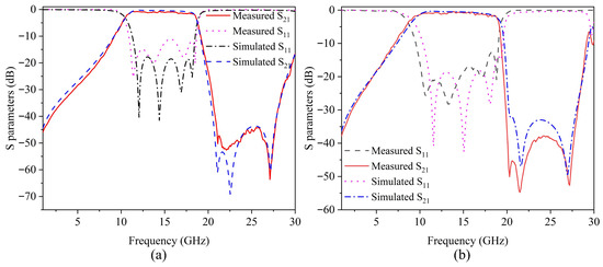
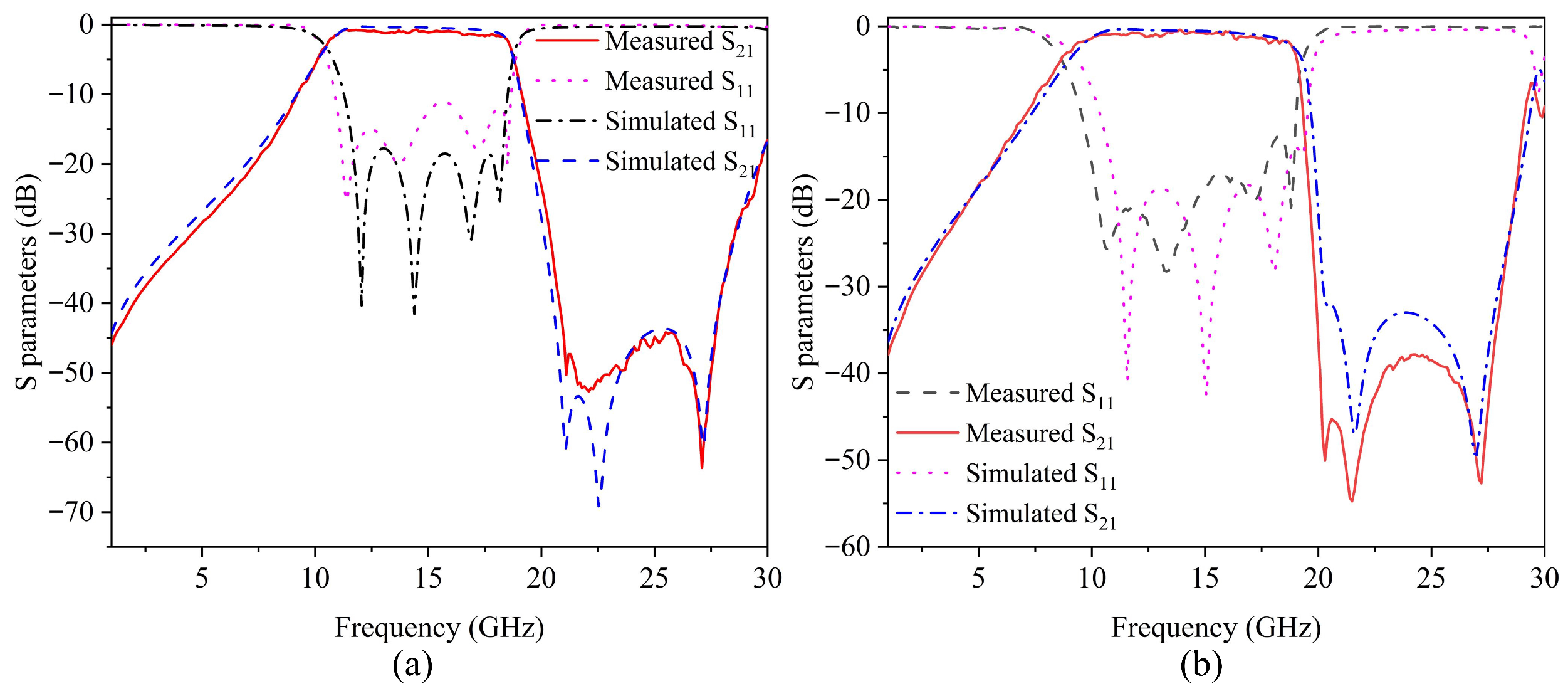
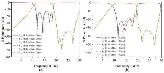
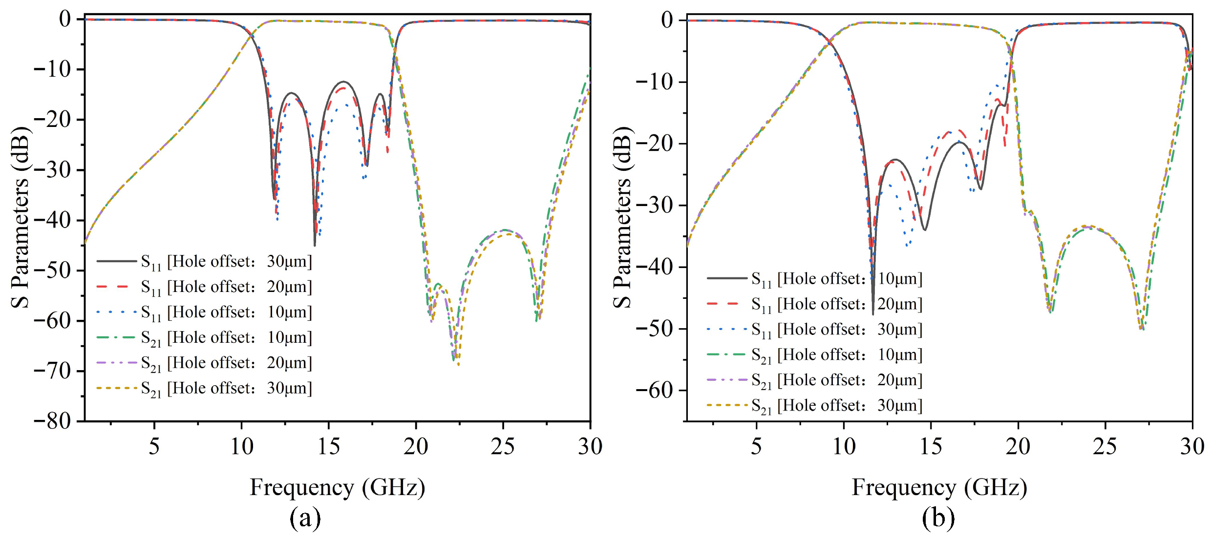
Figure 21a presents a comparison between the simulated and measured results of the IDC-loaded wideband HMSIW filter. The data indicate a strong correlation between the measured and simulated outcomes. The filter demonstrates a passband spanning from 11 to 18 GHz, with a minimum insertion loss within the passband of 0.66 dB and an in-band return loss below −10 dB. Furthermore, the measured response reveals two distinct transmission zeros at 21.1 GHz and 27.1 GHz. The transmission zero around 22.2 GHz is attenuated, likely as a result of fabrication tolerances and measurement losses. These characteristics significantly improve the filter’s out-of-band rejection performance. Figure 21b illustrates the comparison between simulated and measured results for the IDC-loaded SIW filter based on the improved HMSIW transmission line. Similarly, the measured results closely align with the simulations. This filter exhibits a passband range of 10 to 18 GHz, with a minimum in-band insertion loss of 0.58 dB and an in-band return loss better than −13 dB. Furthermore, three transmission zeros located at 20.3 GHz, 21.5 GHz, and 27.1 GHz in the out-of-band region contribute to a marked improvement in the filter’s out-of-band suppression performance. Figure 21 illustrates that the measured S parameters of the filter exhibit a strong overall correspondence with the simulated data; however, the measured in-band return loss demonstrates a slight degradation relative to the simulation results. Both filters developed in this study were fabricated utilizing thin-film technology, which enables pattern fabrication with an accuracy of ±2 μm, a precision level that minimally impacts the overall device performance. In contrast, the positional accuracy of metal vias within the thin-film process is limited to ±30 μm, and deviations in the placement of internal metal vias may negatively influence the in-band return loss of the filter. To elucidate the underlying cause of the observed return loss degradation between experimental measurements and simulations, a simulation-based analysis was conducted to assess the impact of via positional deviations on filter performance. As depicted in Figure 22a, varying degrees of metal via an offset substantially impair the in-band return loss of BPF 1. Similarly, Figure 22b demonstrates that positional deviations of vias also degrade the in-band return loss of BPF 2, although these deviations exert minimal influence on its out-of-band transmission characteristics.
Figure 21.
Comparison between measured and simulated results. (a) Measured and simulated results of IDC-loaded SIW filter based on traditional HMSIW transmission line. (b) Measured and simulated results of IDC-loaded SIW filter based on improved HMSIW transmission line.
Figure 22.
Effect of metal via positioning errors in thin-film process on filter performance. (a) BPF 1. (b) BPF 2.
Table 4 presents a comprehensive comparison of performance metrics and structural dimensions between the IDC-loaded miniaturized wideband HMSIW filters introduced in this study and previously reported wideband SIW filters. The data indicate that the proposed wideband filters exhibit notable improvements in three critical areas: insertion loss, out-of-band suppression, and physical size. To establish a more rigorous and equitable technical benchmark comparison, this study incorporates a manufacturing process dimension alongside the conventional RF performance metrics. Integrating the fundamental preparation steps of thin-film technology, a comprehensive comparative analysis is performed between the proposed filters and other wideband SIW filters fabricated via PCB, redistribution layer (RDL), and through-glass via (TGV) processes. This comparison is conducted across three key aspects: manufacturing complexity, production cost, and process robustness. The bandpass filters (BPF 1 and BPF 2) introduced herein are fabricated using single-layer and double-layer ceramic thin-film processes, respectively. The single-layer process encompasses core steps such as substrate cleaning, magnetron sputtering, photolithography, etching, photoresist removal, metallized via formation, and performance testing. The double-layer process extends this sequence by incorporating anodic bonding. Relative to the three-dimensional packaging inherent in TGV and the wafer-level fine processing characteristic of RDL, the thin-film process presented eliminates the necessity for complex three-dimensional structure fabrication and advanced fine manufacturing techniques, thereby substantially reducing manufacturing complexity. Regarding cost considerations, the process employs alumina ceramic substrates and utilizes conventional RF micro-nano fabrication equipment as its foundation. This results in significantly lower investments in raw materials and equipment compared to TGV and RDL methods. The unit manufacturing cost is situated between those of PCB and RDL processes, offering notable advantages for mass production. In terms of process robustness, the thin-film technique demonstrates considerable tolerance to manufacturing deviations. Furthermore, the alumina ceramic substrate exhibits low dielectric loss and excellent thermal stability, enabling the filter to sustain stable RF performance across a broad temperature range. This environmental adaptability surpasses that of TGV and RDL processes and compensates for the performance stability degradation observed in PCB processes at high frequencies. In summary, the filters introduced in this study preserve the fundamental RF performance benefits, including wide bandwidth, low insertion loss, and compact size. Additionally, they exhibit favorable engineering attributes such as reduced manufacturing complexity, moderate production costs, and enhanced process robustness through the utilization of thin-film technology. These characteristics render the filters highly suitable for integration into high-performance, miniaturized, and mass-producible RF front-end components applicable to 5G/6G networks, satellite communications, and related fields.
Table 4.
Comparison of proposed filters with other wideband SIW filters.
4. Conclusions
This study introduces two compact wideband half-mode substrate-integrated waveguide filters incorporating interdigital capacitor loading. The design and validation processes are conducted in conjunction with ceramic thin-film technology. Initially, the interaction between the IDC bandstop characteristics and the HMSIW highpass properties is examined, leading to the development and verification of an equivalent LC circuit model. Utilizing a multi-resonator electric coupling approach, a triple-IDC-loaded filter (BPF 1) is realized, achieving a fractional bandwidth of 48.3%, a core dimension of , and a measured insertion loss of 0.66 dB. To further enhance miniaturization, a MIM capacitor is integrated at the HMSIW equivalent magnetic wall based on double-layer ceramic thin-film technology. The cutoff frequency equation is derived, and the scaling effect is experimentally confirmed. The resulting improved HMSIW filter (BPF 2) exhibits an increased fractional bandwidth of 57.1%, a reduced size of , a measured insertion loss of 0.58 dB, and three transmission zeros in the out-of-band region to enhance suppression. Fabricated prototypes and measured data for both filters demonstrate strong agreement with simulation results. Compared to existing substrate-integrated waveguide filters reported in the literature, the proposed designs offer notable improvements in bandwidth, compactness, and insertion loss. The broadband SIW filter designs discussed in this study offer efficient approaches for the compact integration of microwave and millimeter-wave radio frequency front-end modules. These configurations are particularly relevant for applications in 5G and 6G wireless networks, satellite communication systems, and other associated domains.
Author Contributions
Conceptualization, L.T.; methodology, L.T. and W.H.; software, L.T. and Q.Z.; validation, L.T. and W.H.; formal analysis, L.T., Q.Z., H.W. (Hao Wei) and Y.L.; investigation, L.T. and W.H.; resources, H.W. (Heng Wei); data curation, L.T. and Q.Z.; writing—original draft preparation, L.T.; writing—review and editing, L.T., W.H. and Q.Z.; visualization, H.W. (Hao Wei), and L.T.; supervision, Y.L.; project administration, H.W. (Heng Wei), and Y.L.; funding acquisition, H.W. (Hao Wei). All authors have read and agreed to the published version of this manuscript.
Funding
This research received no external funding.
Data Availability Statement
We confirm that the data are contained within the article.
Conflicts of Interest
All authors were employed by the company The 54th Research Institute of China Electronics Technology Group Corporation. All authors declare that the research was conducted in the absence of any commercial or financial relationships that could be construed as a potential conflict of interest.
References
- Zhou, T.; Guo, G.; Yang, Z.; Wang, H.; Wang, Z.; Yan, B.; Wei, Y. A Wideband and High-Density Integration Microwave Transceiver Component for Tile-Style Phased Array with SiP Technology. IEEE Microw. Wirel. Technol. Lett. 2025, 1, 1–4. [Google Scholar] [CrossRef] [Scilit]
- Xu, S.; Jin, G.; Lu, D.; Liao, S. Millimeter-wave wideband high-gain LTCC phased array antenna based on ridged substrate integrated waveguide. Int. J. Microw. Wirel. Technol. 2025, 17, 642–652. [Google Scholar] [CrossRef] [Scilit]
- Chen, K.; Xu, J.; Tang, S.Y.; Wang, Y.; Hong, W. Millimeter-wave active beam-tilted phased array modules and seamless integration design with ultrawideband sub-6 GHz antenna for future V2X applications. IEEE Trans. Antennas Propag. 2024, 73, 2737–2753. [Google Scholar] [CrossRef] [Scilit]
- Duraisamy, T.; Kamakshy, S.; Karthikeyan, S.S.; Barik, R.K.; Cheng, Q.S. Compact Wideband SIW Based Bandpass Filter for X, Ku and K Band Applications. Radioengineering 2021, 30, 288–295. [Google Scholar] [CrossRef] [Scilit]
- Nwajana, A.O.; Obi, E.R. A review on SIW and its applications to microwave components. Electronics 2022, 11, 1160. [Google Scholar] [CrossRef] [Scilit]
- Udhayanan, S.; Shambavi, K. Compact single notch UWB bandpass filter with metamaterial and SIW technique. PIER Lett. 2024, 117, 41–46. [Google Scholar] [CrossRef] [Scilit]
- Qiu, L.; Zhu, X.W.; Yang, X.L. Compact multilayer SIW bandpass filter with cross coupling and source-to-multiresonator coupling. IEEE Trans. Compon. Packag. Manuf. Technol. 2024, 14, 2331–2338. [Google Scholar] [CrossRef] [Scilit]
- Fan, G.; He, X.; Ding, D. Dual-Wideband Bandpass Filter in Single SIW Cavity for 5G mmWave Systems. IEEE Trans. Compon. Packag. Manuf. Technol. 2025, 15, 2793–2796. [Google Scholar] [CrossRef] [Scilit]
- Bhardwaj, P.; Deivalakshmi, S.; Pandeeswari, R. Compact wideband substrate integrated waveguide bandpass filter for X/Kuband application. Int. J. RF Microw. Comput. Eng. 2021, 31, 1–10. [Google Scholar]
- Pan, D.; You, B.; Wen, X.; Li, X. Wideband substrate integrated waveguide chip filter using spoof surface plasmon polariton. Micromachines 2022, 13, 1195. [Google Scholar] [CrossRef] [Scilit]
- Tian, H.; Dong, Y. Wideband low-loss filter with compact size and wide stopband based on folded planar waveguide. IEEE Microw. Wirel. Technol. Lett. 2023, 33, 651–654. [Google Scholar] [CrossRef] [Scilit]
- Soundarya, G.; Gunavathi, N. Wideband and highly selective bandpass filter using substrate integrated waveguide technology for ku-band applications. IETE J. Res. 2024, 70, 3476–3482. [Google Scholar] [CrossRef] [Scilit]
- Zhang, W.; Ding, S.; Huang, Y.; Zhu, Z.; He, W.; Bozzi, M. Planar single-/dual-band bandpass filters based on new perturbed multi-mode SIW circular cavity. J. Electromagn. Waves Appl. 2023, 37, 323–334. [Google Scholar] [CrossRef] [Scilit]
- Lu, Q.; Sun, J.; Zhang, H.; Zhang, T.; Zhu, Z. W-band compact triple-mode bandpass filter using multistub resonator in 65-nm CMOS technology. IEEE Microw. Wirel. Technol. Lett. 2024, 34, 1319–1322. [Google Scholar] [CrossRef] [Scilit]
- Wu, L.; Zhang, B.; Li, D.; Niu, Z.; Liu, Y.; He, Z. Single-Cavity Multi-Mode SIW Single/Dual-Band Filter Based on Via-hole Perturbation. In 2024 IEEE MTT-SInternational Microwave Workshop Series on Advanced Materials and Processes for RF and THz Applications (IMWS-AMP); IEEE: Piscataway, NJ, USA, 2024; Volume 1, pp. 1–3. [Google Scholar]
- Chen, R.S.; Wong, S.W.; Zhu, L.; Chu, Q.X. Wideband bandpass filter using U-slotted substrate integrated waveguide (SIW) cavities. IEEE Microw. Wirel. Compon. Lett. 2015, 25, 1–3. [Google Scholar] [CrossRef] [Scilit]
- Azad, A.R.; Kumar, A.; Jhariya, D.K.; Mohan, A. Dual-Mode Wideband Bandpass Filter using Single SIW Cavity with Perturbation Slot. In 2022 8th International Conference on Signal Processing and Communication (ICSC); IEEE: Piscataway, NJ, USA, 2022; Volume 1, pp. 108–111. [Google Scholar]
- Ammari, H.; Riabi, M.L.; Grine, F.; Benhabiles, M.T.; Khalef, R.; Erredir, C. Novel quintuple-mode wideband filter based on substrate integrated waveguide using an elliptic metallic post. In 2018 International Symposium on Antennas and Propagation (ISAP); IEEE: Piscataway, NJ, USA, 2018; Volume 1, pp. 1–2. [Google Scholar]
- He, X.; Ding, D.; Zhang, X.Y. An SIW-based wideband 5G mmWave bandpass filter by using multimode resonator. In 2018 International Symposium on Antennas and Propagation (ISAP); IEEE: New York, NY, USA, 2025; Volume 35, pp. 412–415. [Google Scholar]
- Hong, J.S.; Lancaster, M.J. Transmission Lines and Components. In Microstrip Filters for RF/Microwave Applications; Kai, C., Ed.; John Wiley & Sons: Hoboken, NJ, USA, 2011; pp. 94–95. [Google Scholar]
- Wang, S.; Chung, K.L.; Du, L.; Kong, F.; Li, K. Design and analysis of a compact frequency beam-scanning antenna based on composite FHMSIW/SSPP waveguide. IEEE Antennas Wirel. Propag. Lett. 2022, 21, 546–550. [Google Scholar] [CrossRef] [Scilit]
- Soundarya, G.; Gunavathi, N. Ku-Band SIW filter with high fractional bandwidth optimized using feed forward back propagation ANN. IETE J. Res. 2024, 70, 1272–1282. [Google Scholar] [CrossRef] [Scilit]
- Wang, N.N.; Zhang, D.W.; Liu, Q.; Qian, H.; Qu, W.Z. A compact half-mode substrate integrated waveguide bandpass filter based on highly confined slow waves with loading capacitive patches. IET Microw. Antennas Propag. 2024, 18, 771–778. [Google Scholar] [CrossRef] [Scilit]
- Máximo-Gutiérrez, C.; Hinojosa, J.; Alvarez-Melcon, A. Narrowband and wideband bandpass filters based on empty substrate integrated waveguide loaded with dielectric elements. IEEE Access 2021, 9, 32094–32105. [Google Scholar] [CrossRef] [Scilit]
- Yang, Z.B.; Guan, D.F.; Huang, X.; Zhang, H.C.; You, P.; Xu, S.D.; Liu, L.; Yong, S.W. Compact and wideband octuple-mode filter based on hybrid substrate integrated waveguide and spoof localized surface plasmon structure. IEEE Trans. Circuits Syst. II Express Briefs 2020, 67, 2377–2381. [Google Scholar] [CrossRef] [Scilit]
- Liu, X.; Zhang, Q.; Zhang, T.; Zhang, L.; Liu, N.; Zhu, Z. High Selectivity BPF with Wide-Band and Stopband Exploiting 3D CRLH-SIW in Through Glass Via (TGV)-Based Package. IEEE Trans. Compon. Packag. Manuf. Technol. 2026, 16, 451–454. [Google Scholar] [CrossRef] [Scilit]

Disclaimer/Publisher’s Note: The statements, opinions and data contained in all publications are solely those of the individual author(s) and contributor(s) and not of MDPI and/or the editor(s). MDPI and/or the editor(s) disclaim responsibility for any injury to people or property resulting from any ideas, methods, instructions or products referred to in the content. |
© 2026 by the authors. Licensee MDPI, Basel, Switzerland. This article is an open access article distributed under the terms and conditions of the Creative Commons Attribution (CC BY) license.