


Abstract
This study presents a TCAD model of a SiGe HBT designed for high-speed data transfer, with a cutoff frequency of 246.5 GHz and a β-value up to 416.7. Comprehensive single-event transient (SET) irradiation simulations were performed by injecting charges at different junctions with various angles. The influence of SET on data transfer was further evaluated at circuit level by loading the SET model from TCAD simulation into a high-speed laser diode driver circuit. Hence, this work employed a collector dummy structure in the designed HBT to build radiation-hardened devices. Simulation results indicate significant mitigation of the single-event transient current, which could be reduced to 10%, compared with non-hardened devices.
1. Introduction
Driven by the advancement of artificial intelligence (AI) technology, optical fiber communication offers advantages such as large bandwidth, low power consumption, light weight and anti-interference capability, making it an ideal data transmission approach for data rates over 100 Gbps [1]. As the bandwidth and data rate increase to tens or hundreds of GHz, mixed-signal processing devices, like laser diode drivers (LDDs) and transimpedance amplifiers (TIAs), require transistors to have extremely high cutoff frequencies, which may exceed 300 GHz. A SiGe heterojunction bipolar transistor (HBT) is an ideal device in such applications, capable of providing a cutoff frequency over 350 GHz [2]. Benefiting from the compatibility with traditional CMOS fabrication platforms, SiGe BiCMOS technology has been widely used in the design of RF and optical communication ICs.
In recent years, optical fiber communication devices have also been employed in space payload networking such as high-throughput satellites and communication networks [3,4]. It is noteworthy that in aerospace applications, radiation effects can be harmful to integrated circuits. The presence of single-event effect in a radiation environment, such as digital register upsets and transient currents, can affect the signal quality or even cause the failure of the device. Many investigations have been performed to study the radiation effects on CMOS devices [5,6,7]. Radiation hardening approaches and radiation-hardened device libraries are proposed based on a good understanding of the radiation damage mechanisms, including total ionizing dose (TID) and single-event effect (SEE) [8]. As for the radiation effect on SiGe HBTs, simulation indicates that a SiGe HBT is less sensitive to the TID effect compared to CMOS devices, and the SEE tends to be the major source of damage to SiGe HBTs [9,10,11]. In particular, the single-event transient (SET) effect seems to be critical, as the transient current pulse excited by high-energy particles would mask the data, causing the occurrence of error bits [12]. As the bandwidth of integrated circuits keeps increasing, it is vital to understand the impact of the SET effect on high-frequency SiGe HBTs and explore radiation hardening approaches.
Yet, few studies have been performed to systematically investigate the SET effect for integrated optical communication circuits. A main challenge is to build an HBT model that can accurately describe the behavior of the devices while transferring high-speed data. This is due to the lack of comprehensive modeling information from the manufacturer. Also, it is important to evaluate the SET effects at the circuit level to also illustrate how the SET effect affects the data transfer quality under different ion injection energies and data rates. Such a system, which includes the modeling of an HBT and circuit-level simulation, would also support the evaluation of radiation hardening approaches that are applied to the SiGe HBT, paving the way for designing high-speed data communication ICs for aerospace applications.
In this work, as it is hard to fabricate a proper integrated circuit merely with a physically grown HBT device, a TCAD model of a SiGe HBT is systematically optimized by manipulating the SiGe component, doping concentration and junction depth. The I–V characteristic and frequency performance are studied so as to predict a SiGe HBT device model that works at high cutoff frequencies. A peak frequency of 246.5 GHz and a β-value up to 416.7 are obtained by optimizing a 2D SiGe HBT model, which could well support the design of high-speed laser diode driver circuits with data rate increases over 25 Gbps. Moreover, the single-event transient (SET) response of a SiGe HBT is simulated with frequency dependency which indicates the sensitive area of the SiGe HBT. Building upon this, the impact of the SET effect on high-speed data transfer for the laser driver circuit constructed with SiGe HBT devices is observed. This work also proposes a SiGe HBT hardening approach using a dummy collector. Validation results show that the transient current after hardening is reduced by over 90%, while maintaining the original DC and AC characteristics.
2. Design of Device Structure and Laser Driver Circuit
2.1. The Design of SiGe HBT Device with TCAD
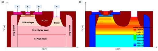
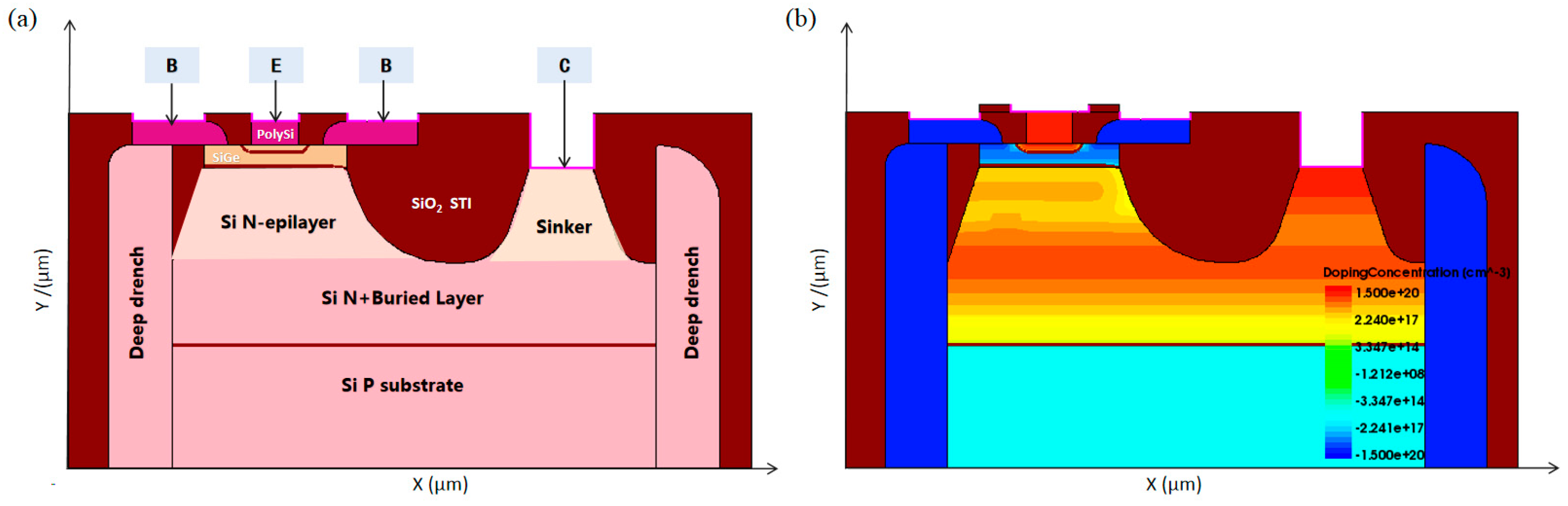
The 2D structural model of the SiGe HBT, constructed using the TCAD simulation tool, is shown in Figure 1. A 0.18 μm double-base SiGe HBT device model is built with a composition-graded Si1−xGex layer, and the active area dimensions are 6 μm × 3.5 μm. Herein, boron is selected as the doping material for the base region and substrate, while arsenic is chosen as the doping material for the emitter and collector regions. The Gaussian doping is applied to all active regions. The emitter-centered doping concentration is set to 5.19 × 1019 cm−3, and the base-centered doping concentration to 4 × 1018 cm−3, in order to reduce parasitic resistances between the base–collector and base–emitter junctions. The collector region can be divided into a collector contact region and a buried layer region. The doping concentration decreases gradually from 1019 cm−3 at the collector center to 7 × 1016 cm−3 at the substrate edge. The peak doping concentration in the external collector region’s contact layer reaches 1.1 × 1020 cm−3.
Figure 1.
(a) 2D structural model of the device constructed by the TCAD simulation tool; (b) doping profile of the HBT model.
All active regions are grown on a P-type substrate, and polysilicon is used to cover the top of the emitter and base regions for electrode contact extraction. The composition percentage of SiGe is given as Si0.75Ge0.25 so as to achieve the optimized AC characteristics and noise characteristics [13]. Following conventional SiGe HBT fabrication processes, a deep trench isolation (DTI) layer and a shallow trench isolation (STI) layer are designed for isolation.
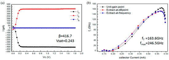
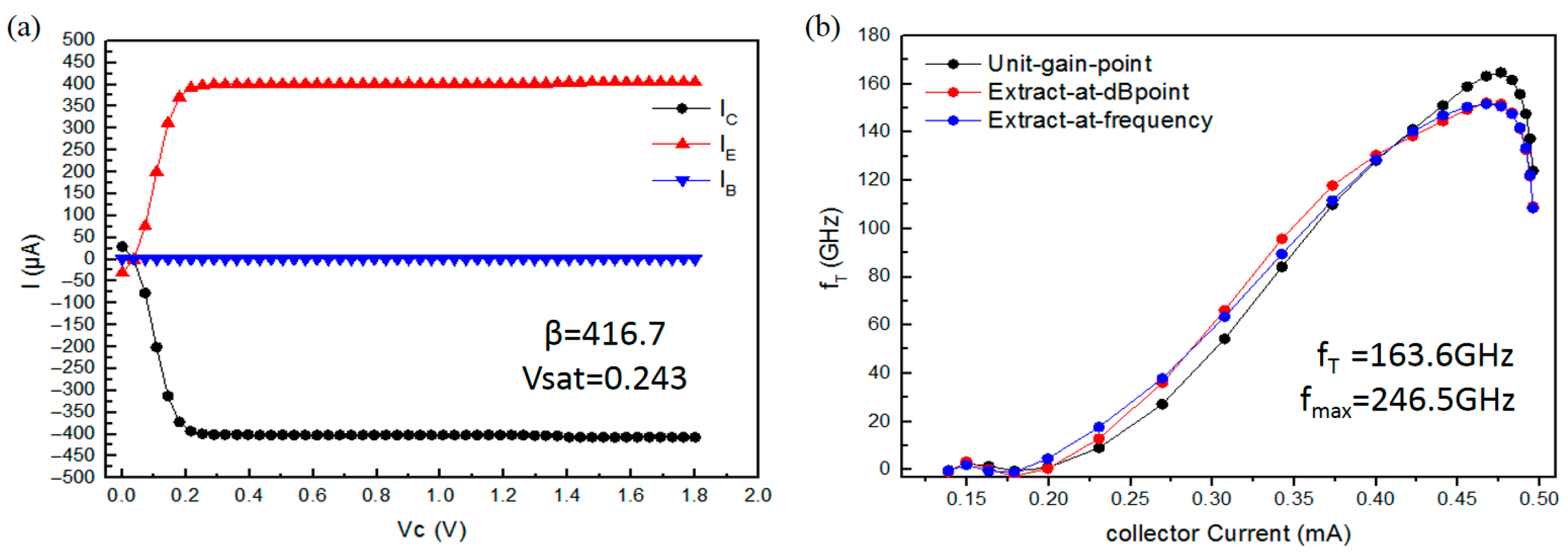
The drift-diffusion model and the Auger and SRH (Shockley–Read–Hall) recombination models are employed in this study [14]. The velocity saturation model and Slotboom bandgap narrowing model are also considered during the simulation. The simulation conditions for the electrical characteristics were set as follows: VCE = 1.8 V, Ib = 1 μA. For the DC and AC simulation, as shown in Figure 2, the HBT model exhibits a current gain (β) of 416.7, with a transition frequency (fT) of 163.6 GHz, and a cutoff frequency (fMAX) of 246.5 GHz.
Figure 2.
(a) Gummel characteristics of HBT model; (b) frequency characteristics of HBT model.
2.2. The Design of Laser Driver Circuit
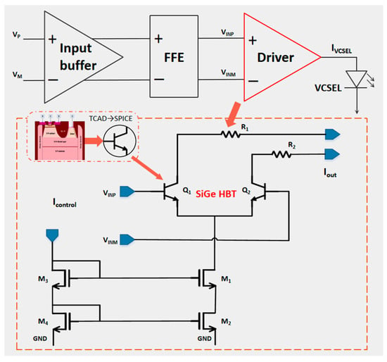
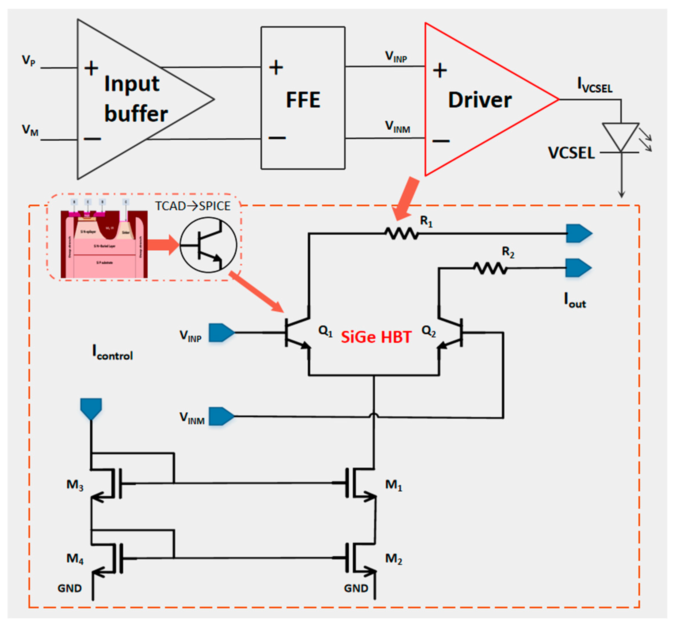
In the area of optical communication, SiGe BiCMOS technology has been widely used for its high frequency performance. Herein a VCSEL driver circuit is designed with the designed SiGe HBT shown in Figure 1. The driver circuit primarily consists of four main components: an input buffer, a Feed-Forward Equalizer (FFE), an output current drive circuit, and an effective vertical cavity surface emitting laser (VCSEL). The functional circuit block for front-end channel signal equalization is not considered in this paper so as to simplify the data transfer process. The reason for choosing VCSEL is its compact size, low cost, and ease of integration, which make it popular in aerospace fiber optic communication systems.
In the driver circuit, 25 Gbps differential CML (Current Mode Logic) signals with a peak-to-peak amplitude of 200 mV are sent to an input buffer and a Feed-Forward Equalizer (FFE) module to compensate for the loss of high-frequency signals. Subsequently, the output stage injects modulation current into the VCSEL by converting the tail current with the high-speed differential voltage signals.
The driver circuit provides the laser diode with bias and modulation currents, the current of the VCSEL is shown in Formula (1) [15],
The output stage of the driver should satisfy the requirements of high gain, wide bandwidth and good linearity. The Current Mode Logic (CML) structure is commonly used in the output drive stage of optical modulators [16]. Figure 3 illustrates the output current drive circuit employs a two-stage CML differential architecture with AC-coupled modulation; the input signals steer the tail current by switching the SiGe HBT differential pair, enabling 25 Gbps current modulation.
Figure 3.
Driver circuit implemented with SiGe HBT model.
To substitute the designed TCAD SiGe HBT device into a laser driver circuit, a parameter extraction method was employed to obtain the key electrical parameters of the established SiGe HBT model. A compact model was then utilized to construct the corresponding SPICE equivalent circuit, thereby enabling the translation from the TCAD device model to the Virtuoso circuit platform. Initially, in the Sentaurus TCAD software 2016, the DC, AC, and transient self-heating characteristics of the device were simulated over typical bias points and frequency ranges. From these simulations, characteristic parameters including the transfer current parameters, internal and external resistances of each region, junction capacitances, grading factors, built-in potentials, and small-signal transconductance were extracted. Subsequently, to meet the performance requirements of hundred-gigabit-per-second SiGe HBT devices, the HICUM model, which offers the highest physical scalability and superior high-frequency accuracy, was selected as the compact model template for the SPICE equivalent implementation of the device [17]. Finally, the established TCAD SiGe HBT device model was equivalently converted into a SPICE model and integrated as a circuit component into the laser driver circuit, as illustrated in Figure 3.
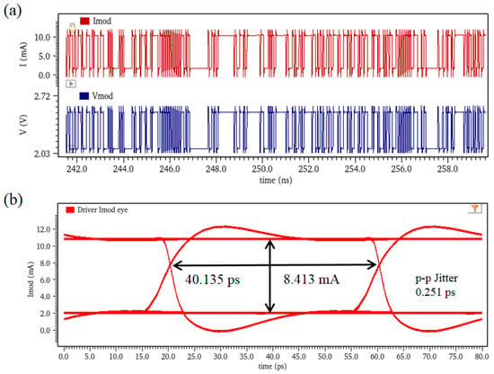
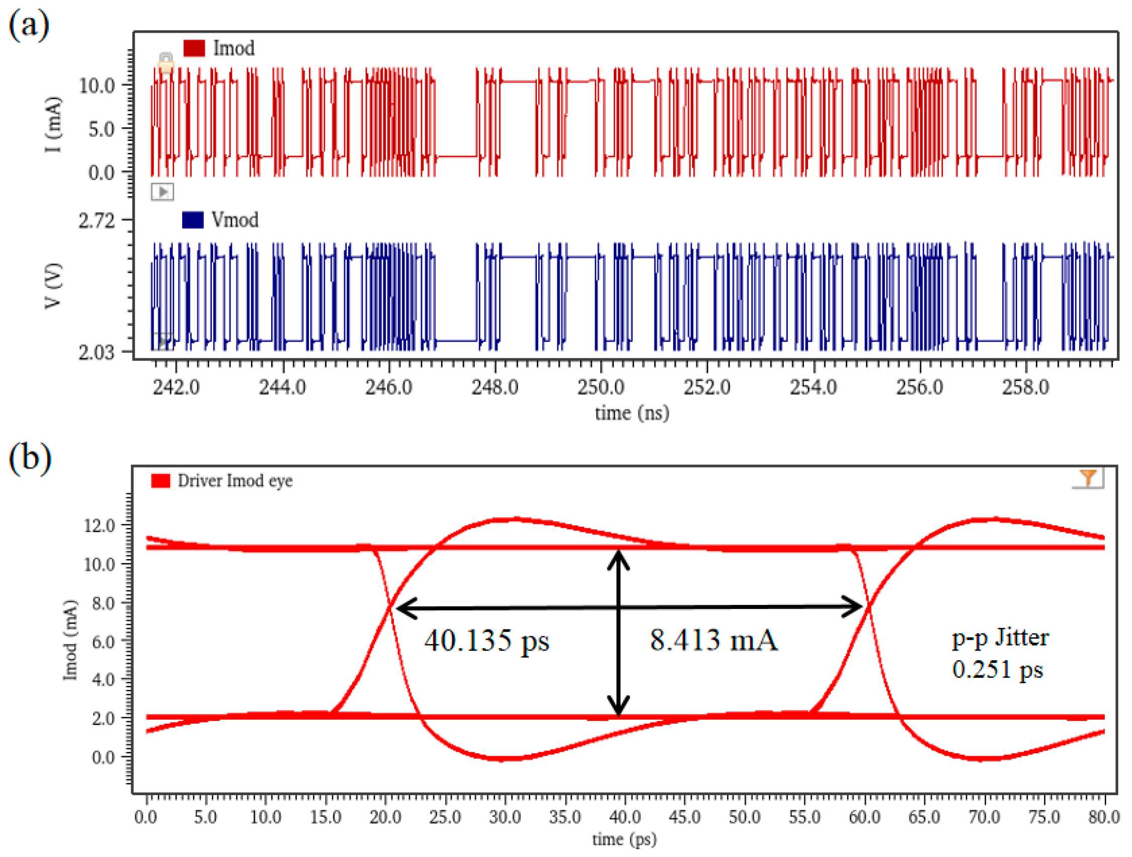
The performance of the driver circuit was simulated through Virtuoso software 2016, using an output load impedance of 80 Ω. Differential 25 Gbps NRZ signals with 0.25 Vpp were input to VP and VM. Under the TT corner and a temperature of 27 °C, the simulation results of the waveforms at IOUT and VOUT are shown in Figure 4a, while the eye diagram of the modulation current appears in Figure 4b. The eye diagram exhibits a clear opening with an 8.413 mA eye height and 0.251 ps peak-to-peak jitter. The total bias current of 6.6 mA is suitable for driving VCSEL diodes.
Figure 4.
(a) Transient response of modulation current output; (b) corresponding eye diagram.
3. Radiation Simulation of Device and High-Speed Mixed Signal
3.1. Radiation Simulation of SiGe HBT
For laser diode driver circuits, the response characteristics of SiGe HBT devices under irradiation are of critical importance to their overall reliability. In the complex space radiation environment, various functional modules of the circuit are threatened by random single-event effects. To deeply investigate the damage mechanisms of devices and circuits under single-event irradiation, this paper systematically studies the influence of key parameters such as incident location, incident angle, and linear energy transfer (LET) on the single-event effects in SiGe HBTs.
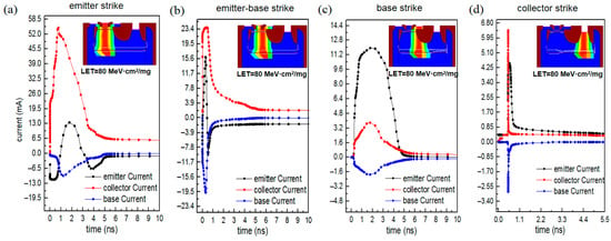
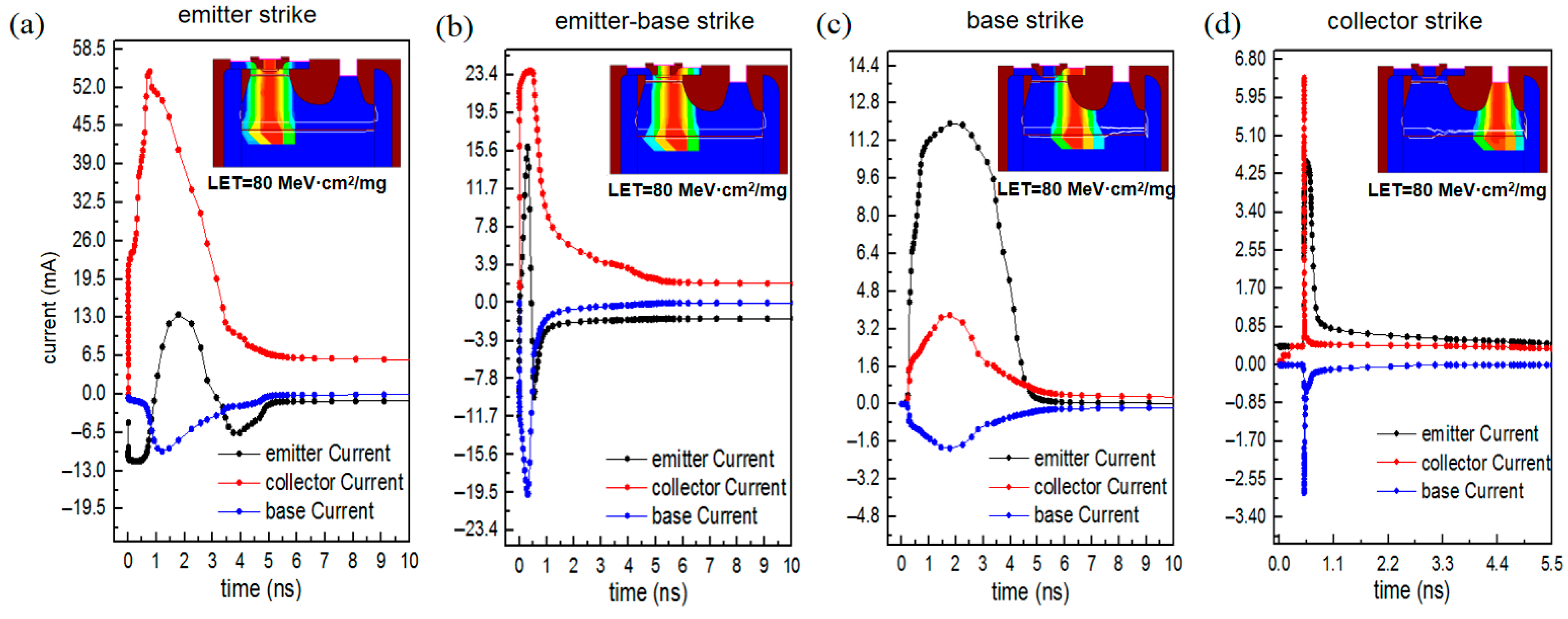
The analysis begins with the impact of the incident location. Considering that the emitter, base–emitter junction region, base, and collector are the most sensitive structural regions of the SiGe HBT device to single-event effects [18], these four typical locations were selected as the vertical incidence points for heavy ions to comprehensively evaluate the evolution of the single-event response with varying incident positions. To simulate the extreme ionization damage potentially induced by heavy ions in space, and thereby assess the saturation characteristics of single-event effects in SiGe HBT devices under the most severe irradiation conditions, the LET value of the incident particles was set to the typical value for high-energy heavy ions of 80 MeV·cm2/mg [19]. In the simulation, the characteristic radius of the incident track was set to 0.1 μm, the incident duration was 0.1 ns, and a Gaussian distribution model was adopted to describe the radial distribution of charge deposition. A series of simulations shows that the injection of heavy ions would induce a transient current with a different response time, pulse width, and recovery time, which are shown in Figure 5a–d.
Figure 5.
Transient currents of different terminals which strike (a) the emitter; (b) the middle of the emitter and base; (c) the base; and (d) the collector.
For the particles that strike the emitter of the HBT, they could create a strong current pulse at the collector, with a peak current of 54.3 mA, which occurs 100 ps after the ions are injected and recovered in 4.95 ns. Similarly, particles striking between the emitter and base induce a transient pulse with a 23.4 mA peak current and recovers within ~7 ns. This is due to the fact that particles striking around the emitter travel through a long electric field that includes the EB junction, BC junction, buried layer and substrate [20].
While particles strike the base, the transient current seems to be less sensitive, since some of the injected particles are blocked by the deep trench [21]. It is noteworthy that the base current is larger than the collector and emitter currents in the base strike situation. This is because the transient current at the emitter is much greater than that at the collector which forward biases the EB junction [22]. Moreover, due to the fact that the penetration path from collector injection only passes through the collector and the substrate, the collector of the SiGe HBT is less sensitive to the strike of heavy ions [23]. As shown in Figure 5d, heavy ions with an LET of 80 MeV cm2/mg induce a transient peak current of only 5 mA and recover immediately in 258 ps.
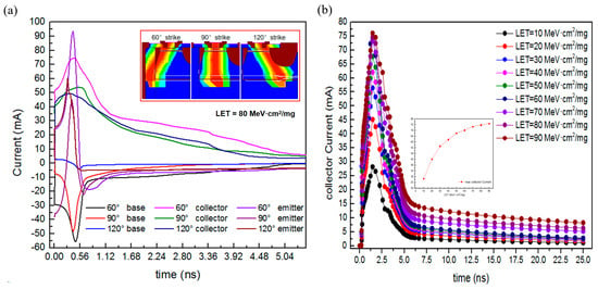
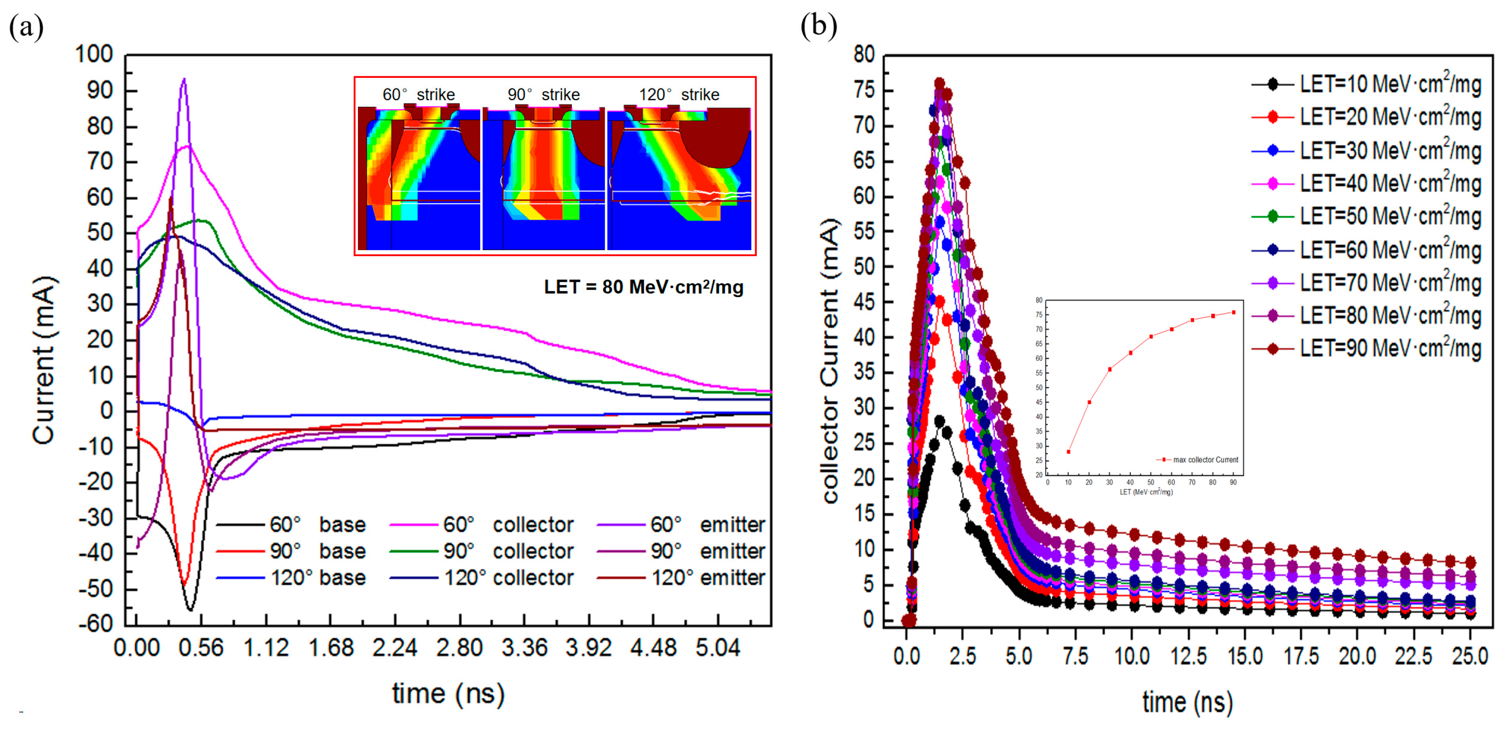
Herein, we choose the most sensitive area, the emitter of the HBT, as the striking position and investigate the influence of the striking angle. According to the insertion in Figure 6a, angles of 60°, 90°, and 120° are simulated. The pink curve in Figure 6a indicates that a 60° striking angle could produce the largest emitter transient current of 95 mA. This simulation result is in good consistency with the assumption in previous discussions. Changing the striking angle to 60° further increases the travel path of the heavy ions, covering nearly the whole EB and BC junction, which enhances the interaction between heavy ions and the electrical field at these two junctions. Although a striking angle of 120° also increases the particle travel length, most of the particles only pass through the substrate, producing a less transient current than that with the 60° striking angle.
Figure 6.
(a) Transient currents of different terminals at different strike angles; (b) the transient current of the collector under different LET values.
To comprehensively cover the space radiation environment, multiple LET values were set for simulation validation. When the LET value falls below a certain threshold, the charge deposited by the incident particle in the sensitive volume is insufficient to induce single-event effects. Therefore, a typical LET value of 10 MeV cm2/mg, corresponding to lighter heavy ions such as neon [24], was selected as the lower limit for the simulation parameters. One of the most damaging particles in space is the gold (Au) ions present in galactic cosmic rays, which have typical LET values of approximately 90 MeV cm2/mg [25]. Choosing 90 MeV cm2/mg as the upper limit ensures that the simulation can account for the potential extreme damage caused to the device by high-LET ions.
Given an emitter striking angle of 60°, we scan the LET value from 10 to 90 MeV cm2/mg, and plot the transient collector current in Figure 6b. The peak current and recovery time both increase as the LET value rises, which is due to the fact that higher LET enhances the interaction between the injected ions and the electrical field. The transient current tends to saturate at higher LET, since the number of electron-hole pairs at the depletion region is saturated, limiting the increase in current density [26].
To validate the credibility of the simulation results, typical SiGe HBT SET simulation and measurement results published within the past two years are summarized in Table 1 and compared with the findings of this work.
Table 1.
Comparison of SiGe HBT SET characteristics between published data and this study.
3.2. Radiation Simulation of Laser Driver Circuit
The SET effect is also demonstrated at the circuit level with the same laser driver circuit by replacing the HBT models with the SPICE model obtained after SET simulation. Three radiation mechanisms are extracted into the SPICE model, which are high-energy particles injected at the emitter at a 60° injection angle, between the emitter and the base at a 90° injection angle, and at the base at a 90° injection angle.
To simulate the intensity of single-particle beams in a space environment, ground tests and existing research conclusions generally select particle injection frequencies ranging from 105/cm2/s to 108/cm2/s [31]. In order to obtain valid statistical data within an acceptable timeframe while ensuring the physical authenticity of the experiment, the pulse rate is set to 107/cm2/s to be equivalent to the cosmic rays in the space environment. The effective transient current at each junction is approximated by a set of individual current sources that are added to the emitter, collector and base of the designed HBT at the circuit level.
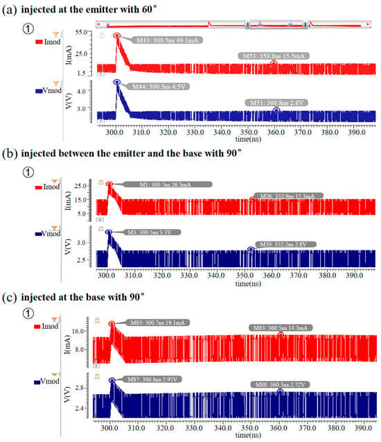
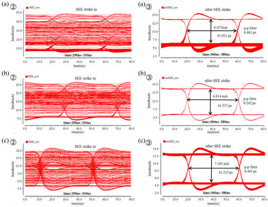
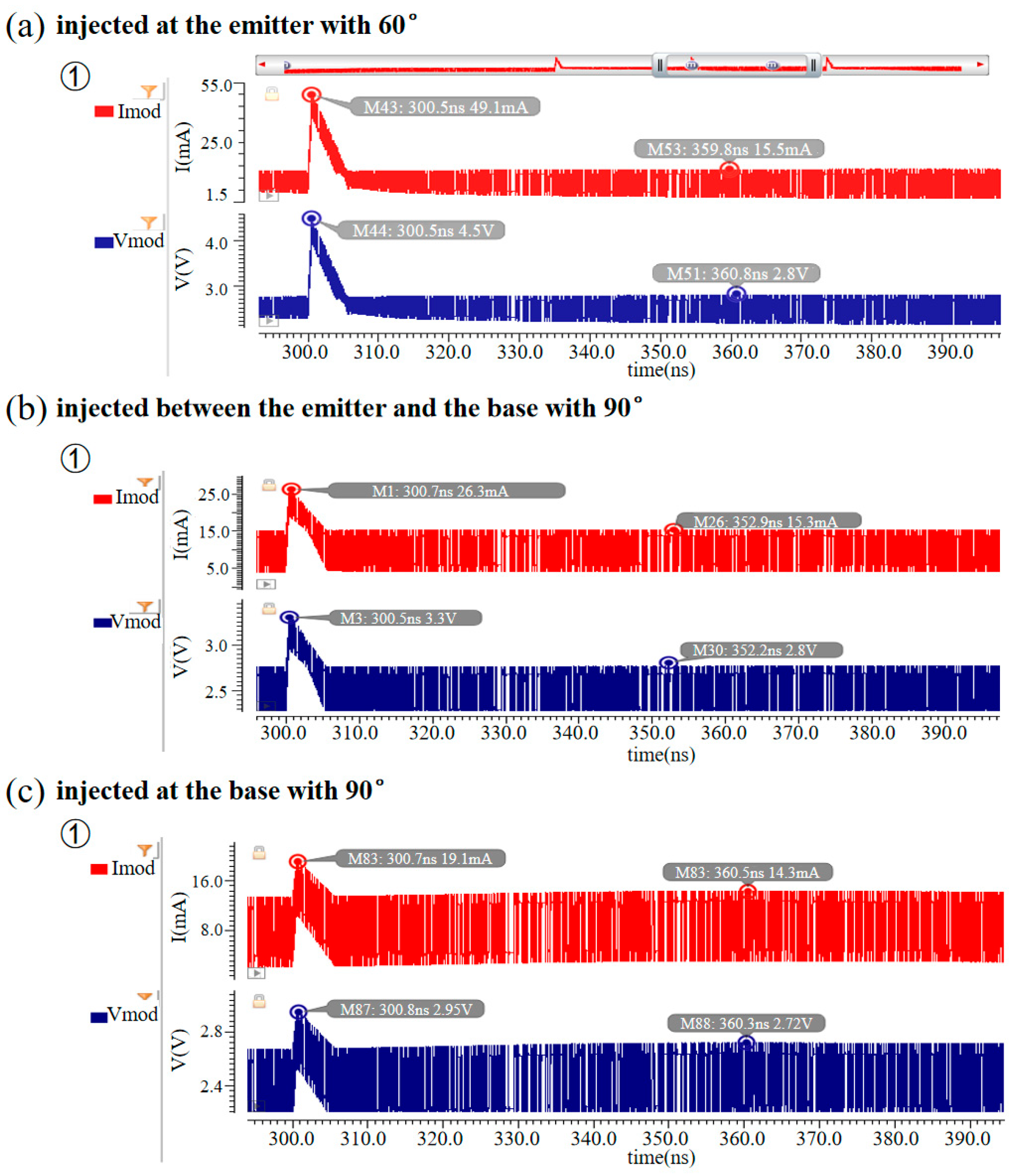
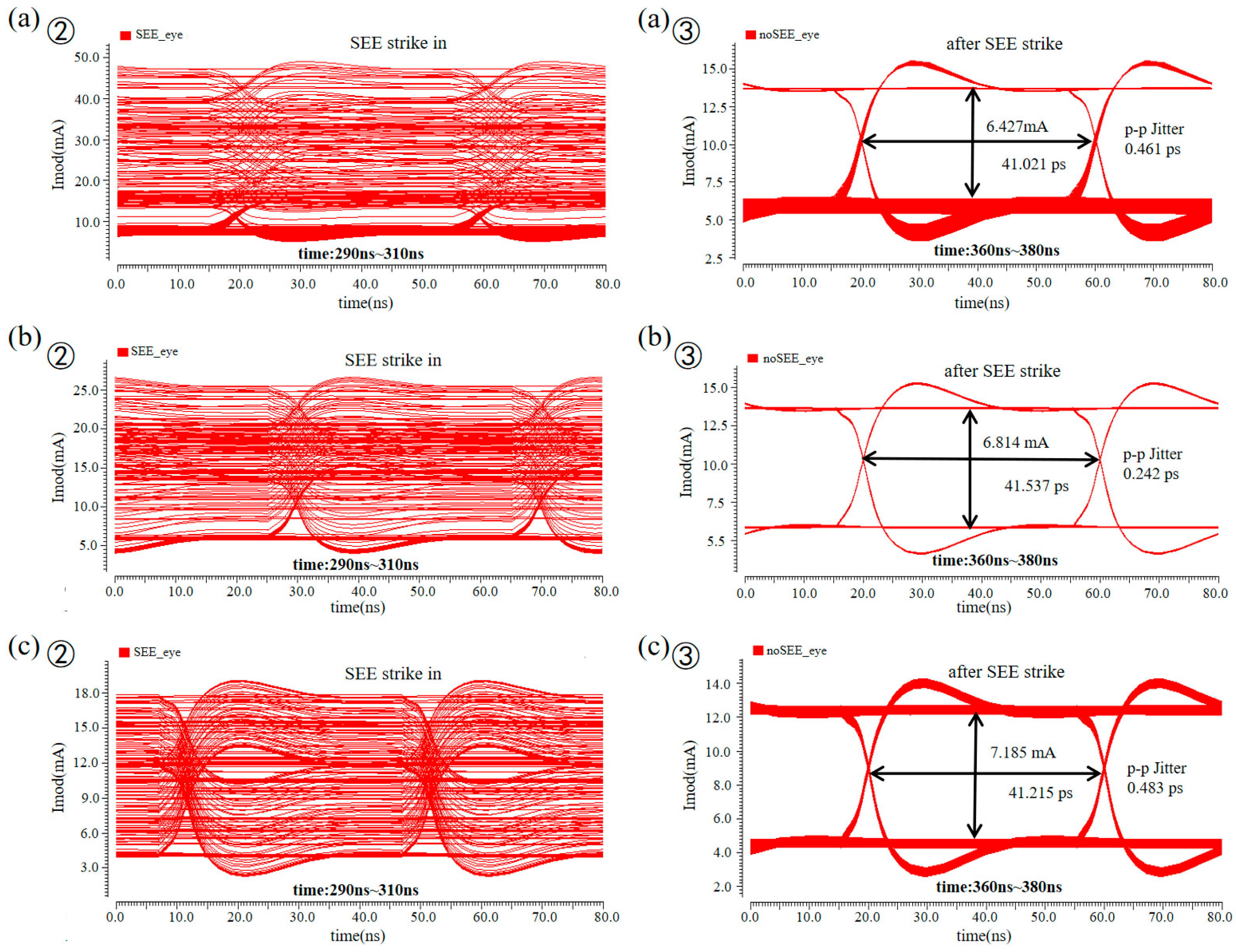
Figure 7 illustrates the transient waveform of the modulation current while a SET excitation is given at 300 ns. Figure 7(a)①, (b)①, and (c)① show the modulation current transient waveform during a single-particle strike event and the subsequent circuit recovery sequence. Since the injection of heavy ions induces a large transient current at the collector, the modulation current from the tail current source is added to such a transient current before it flows into the laser diode. For different injection mechanisms, the transient pulses produce various intensities and recovery times. That is in good agreement with the SET simulation result at the device level. It is worth noting that any SET process could cause a strong perturbation to the quality of the eye diagram. The eye diagram’s quality is also collected after the SET pulse is recovered in Figure 7(a)③, (b)③, and (c)③. The circuit functions in the three experimental groups gradually stabilized. Based on the simulation, we can observe that single-event effects cause a significant degradation in signal integrity for the laser driver circuit, substantially compromising its performance. According to those simulation results above, the recovery time and SET intensity determine the quantity of data are masked by the transient pulse, which means the SET effect is rather harmful for circuits with high data rates.
Figure 7.
Modulation current transient waveform and eye diagram of the laser driver circuit. Injected (a) at the emitter with 60° injection angle; (b) between the emitter and base with 90° injection angle; (c) at the base with 90° injection angle.
4. Hardening the Device
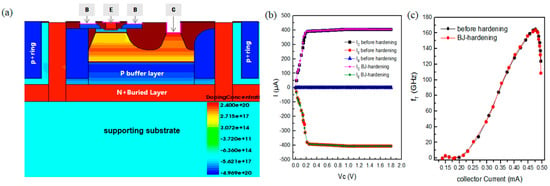
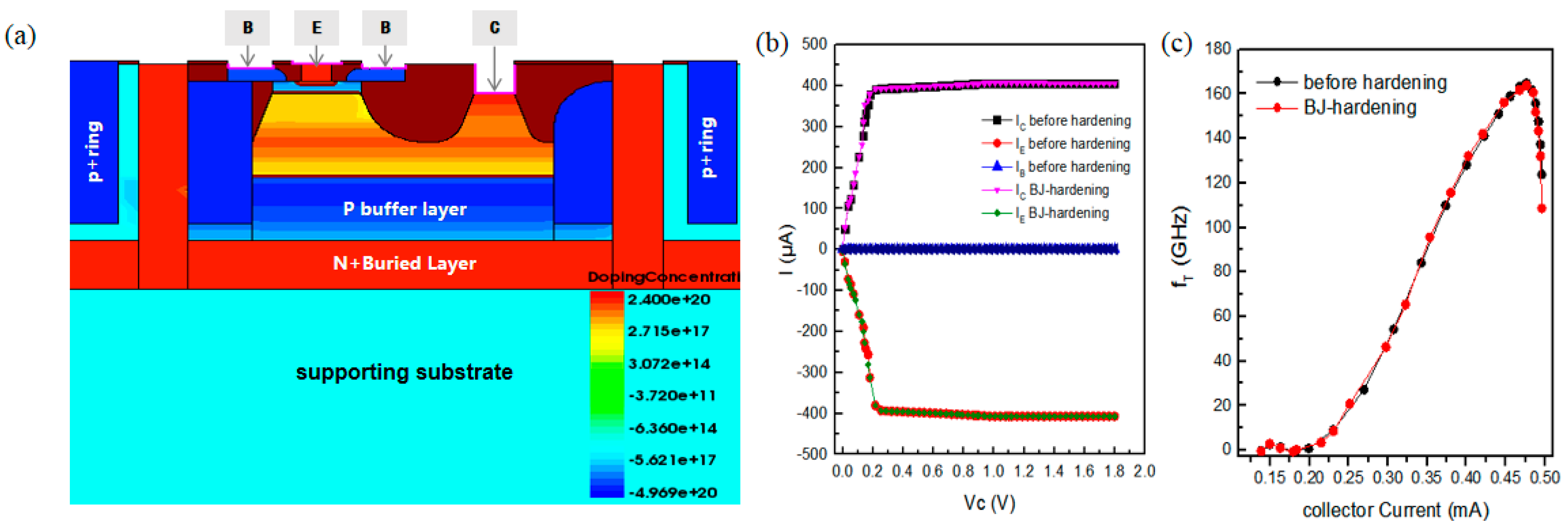
As the SET effect mainly occurs at the collector–substrate junction, an effective way of radiation hardening is to introduce an additional reverse-biased p-n junction with the p-substrate and an n+ guard ring to absorb the unwanted transient current [32]. The biased p-n junction designed in this work, the namely dummy collector, is shown in Figure 8a. The high-frequency characteristic of the SiGe HBT device model is again simulated to prove that the dummy collector does not affect the cutoff frequency (fT) and Gummel behavior, as shown in Figure 8b,c.
Figure 8.
(a) Cross-section view of the dummy collector; (b) frequency characteristics of the dummy collector HBT; and (c) HBT Gummel characteristics.
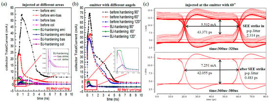
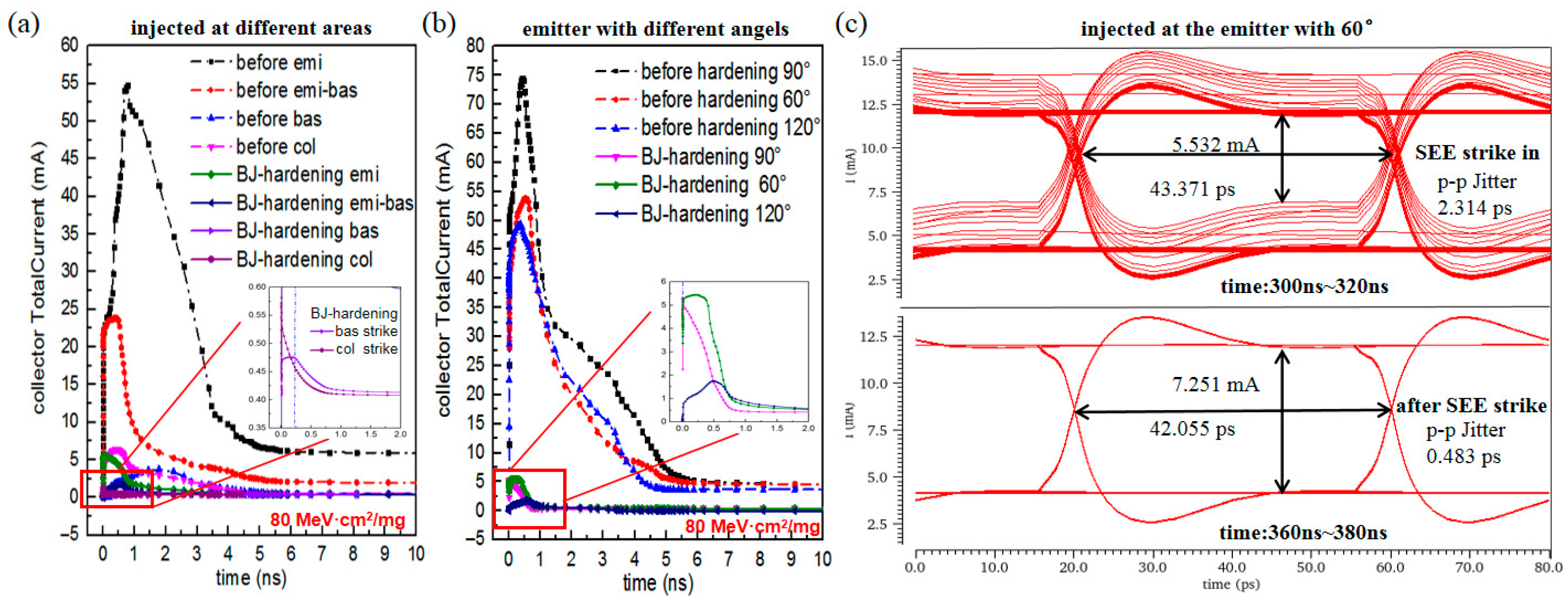
Figure 9a shows the variations in transient current at different ion strike positions with time dependence. The LET is set to 80 MeV cm2/mg to maintain consistency. The transient current under emitter striking mode decreases from 54.3 mA to 5.52 mA, and recovers 1 ns after the ion strikes. Also, the transient current of base and collector striking decreases to 0.45 mA with the dummy collector, hardly affecting the circuit. We also analyzed the effects of striking angles, including 60°, 90°, and 120°. According to the inset in Figure 9b, for the emitter striking angle of 60°, the most sensitive injection, the transient current is reduced by 92.66% compared to the device without the hardening.
Figure 9.
(a) Transient currents of the collector for different ion incident positions; (b) transient currents of the collector for different ion incident angles at the emitter; (c) the eye diagram of emissions striking at 60° and after the SEE pulse.
To compare the post-irradiation response performance of devices after hardening the laser driver circuits, the SPICE model of the hardened device is extracted to simulate the high-speed signal circuit. The eye diagram with an emitter striking angle of 60° is illustrated in Figure 9c. A significant improvement in eye quality is observed, indicating that signal integrity is much better with the radiation-hardened SiGe HBT.
5. Conclusions
This paper presents a systematic study of the radiation effect on high-speed SiGe HBT devices, as most of the radiation effect simulation and hardening work on SiGe HBTs focuses on the device level. It is worth investigating the impact of radiation from the perspective of the circuit level to illustrate the signal integrity degradation mechanism. In this work, a SiGe HBT model is built with Sentaurus TCAD in the first place to simulate a typical high-speed SiGe HBT. The high-speed data transfer capability is validated via a 25 Gbps differential laser diode driver circuit in which SiGe HBT is utilized to convert tail current. Furthermore, the single-event transient effect under high-energy particle radiation is investigated, and different striking mechanisms are simulated with various LET values. Simulation results demonstrate that the emitter of the designed HBT is the area most sensitive to radiation, which is because the particles have the longest interaction path with the electric field of the HBT junctions. Moreover, this work performs a circuit-level simulation to demonstrate the influence of the SET effect on a high-speed digital data transfer circuit. The SPICE models after radiation are extracted and loaded back to the laser diode driver circuit. The transient waveform of the modulation current indicates that the occurrence of a SET pulse would mask part of the data to be transferred which will result in a chain of error bits. Although some error correction algorithm could correct the error, the random appearance of a SET pulse could still severely affect the quality of data transfer in the aerospace environment. This work implemented dummy collector structures onto the SiGe HBT to mitigate the impact of the SET process, which effectively reduces the transient pulse. Further efforts will focus on experimental validation of the hardened design and thus validate the effectiveness of different radiation hardening approaches.
Author Contributions
Conceptualization, Z.Q. and C.L.; methodology, Z.Q., C.F., F.Z., C.L.; software, Z.Q. and J.Z.; validation, Z.Q., C.F., Y.Z., F.Z., C.L., S.S.; formal analysis, Z.Q., Y.Z., F.Z., C.F.; investigation, Z.Q., C.F., Y.Z., F.Z., S.S., J.Z.; resources, Z.Q.; data curation, Z.Q.; writing—original draft preparation, Z.Q., C.F., C.L.; writing—review and editing, Z.Q., Y.Z., C.L. All authors have read and agreed to the published version of the manuscript.
Funding
This research received no external funding.
Data Availability Statement
The original contributions presented in this study are included in the article. Further inquiries can be directed to the corresponding author.
Acknowledgments
The authors would like to express their gratitude to the Beijing Microelectronic Technology Institute and Beihang University for providing the research conditions.
Conflicts of Interest
The authors declare no conflicts of interest.
References
- Wang, Z.; Choi, M.; Lee, K.; Park, K.; Liu, Z.; Biswas, A.; Han, J.; Du, S.; Alon, E. An Output Bandwidth Optimized 200-Gb/s PAM-4 100-Gb/s NRZ Transmitter with 5-Tap FFE in 28-nm CMOS. IEEE J. Solid-State Circuits 2022, 57, 21–31. [Google Scholar] [CrossRef] [Scilit]
- Pekarik, J.; Jain, V.; Kenney, C.; Holt, J.; Khokale, S.; Saroop, S.; Johnson, J.B.; Stein, K.; Ontalus, V.; Durcan, C.; et al. SiGe HBTs with fT/fmax~375/510 GHz integrated in 45nm PDSOI CMOS. In Proceedings of the IEEE BCICTS, Monterey, CA, USA, 5–8 December 2021; pp. 1–4. [Google Scholar]
- Giannakopoulos, S.; Schmitz, A.; Liero, A.; Bielik, M.; Rödiger, J.; Fraschke, M.; Borngräber, J.; Sperling, M.; Plettemeier, D.; Heinrich, W.; et al. A 112 Gb/s Radiation-Hardened Mid-Board Optical Transceiver in 130-nm SiGe BiCMOS for Intra-Satellite Links. Front. Phys. 2021, 9, 672941. [Google Scholar] [CrossRef] [Scilit]
- Tee, C.A.T.; Majlis, B.Y.; Li, S.; Sun, H.B.; Buyong, M.R.; Song, L.; Yeo, W.P.; Zain, A.R.M.; Zheng, Y. VCSELs-based optoelectronics transceiver for free space photonics packet switching network. In Proceedings of the IEEE ICSE, Kuala Lumpur, Malaysia, 19–21 August 2024; pp. 52–55. [Google Scholar]
- Chen, Q.; Sun, Q.; Zhao, C.; Guo, D.; Gong, D.; Liu, C.; Liu, T.; Sun, X.; Xiao, L.; Ye, J. A 14-Gbps VCSEL driver in 65 nm CMOS with a power-efficient driving structure for particle physics experiments. IEEE Trans. Nucl. Sci. 2023, 70, 1065–1073. [Google Scholar] [CrossRef] [Scilit]
- Borghello, G.; Ceresa, D.; Peja, R.; Diaz, F.P.; Bergamin, G.; Kloukinas, K. Single event effects characterization of a commercial 28 nm CMOS technology. In Proceedings of the TWEPP 2023 Topical Workshop on Electronics for Particle Physics (TWEPP), Geremeas, Italy, 1–6 October 2023; pp. 28–31. [Google Scholar]
- Zhang, C.M.; Jazaeri, F.; Pezzotta, A.; Bruschini, C.; Borghello, G.; Faccio, F.; Mattiazzo, S.; Baschirotto, A.; Enz, C. GigaRad total ionizing dose and postirradiation effects on 28 nm bulk MOSFETs. In Proceedings of the 2016 IEEE Nuclear Science Symposium, Medical Imaging Conference and Room-Temperature Semiconductor Detector Workshop (NSS/MIC/RTSD), Strasbourg, France, 29 October 2016–6 November 2016; pp. 1–4. [Google Scholar]
- Liang, B.; Chen, J.; Chi, Y.; Yuan, H.; Wen, Y.; Yao, X.; Sun, H. SEE and TID characterization of an 8 Gbps SST transmitter in a 28 nm bulk CMOS technology. Microelectron. Rel. 2023, 142, 114909. [Google Scholar] [CrossRef] [Scilit]
- Boulgheb, A.; Lakhdara, M.; Latreche, S. Improvement of the self-heating performance of an advanced SiGe HBT transistor through the Peltier effect. IEEE Trans. Electron Devices 2021, 68, 479–484. [Google Scholar] [CrossRef] [Scilit]
- Li, P.; He, C.; Guo, H.; Li, Y.; Wei, J. Synergistic effects of ionizing dose and displacement damage on SiGe heterojunction bipolar transistors. IEEE Trans. Nucl. Sci. 2022, 69, 1051–1056. [Google Scholar] [CrossRef] [Scilit]
- Baszczyk, M.; Biereigel, S.; Klekotko, A.; Kulis, S.; Martina, F.; Moreira, P. Dual use driver for high speed links transmitters in the future high energy physics experiments. J. Instrum. 2024, 19, C03013. [Google Scholar] [CrossRef] [Scilit]
- Ildefonso, A.; Fleetwood, Z.E.; Tzintzarov, G.N.; Hales, J.M.; Nergui, D.; Frounchi, M.; Khachatrian, A.; Buchner, S.P.; Mcmorrow, D.; Warner, J.H.; et al. Optimizing optical parameters to facilitate correlation of laser- and heavy-ion-induced single-event transients in SiGe HBTs. IEEE Trans. Nucl. Sci. 2019, 66, 359–367. [Google Scholar] [CrossRef] [Scilit]
- Wei, J.; Li, Y.; Yang, W.; He, C.; Li, Y.; Zang, H.; Li, P.; Zhang, J.; Guo, G. Proton-induced current transient in SiGe HBT and charge collection model based on Monte Carlo simulation. Sci. China Technol. Sci. 2020, 63, 851–858. [Google Scholar] [CrossRef] [Scilit]
- Petrosyants, K.; Torgovnikov, R. Electro-thermal modeling of trench-isolated SiGe HBTs using TCAD. In Proceedings of the 2015 31st Thermal Measurement, Modeling & Management Symposium (SEMI-THERM), San Jose, CA, USA, 15–19 March 2015; pp. 172–175. [Google Scholar]
- Wu, T.Y.; Jou, J.J.; Shih, T.T.; Chiang, P.J.; Wu, Y.D. Design of a 25-Gb/s PAM-4 VCSEL Diode Driver with an Equalizer in 90-nm CMOS Technology. In Proceedings of the 2019 IEEE International Symposium on Circuits and Systems (ISCAS), Sapporo, Japan, 26–29 May 2019; pp. 1–4. [Google Scholar]
- Mansuri, M.; Inti, R.; Kennedy, J.; Qiu, C.; Hsu, M.H.; Shama, J.; Li, H.; Casper, B.; Jaussi, J. A Scalable 32–56 Gb/s 0.56–1.28 pJ/b Voltage-Mode VCSEL-Based Optical Transmitter in 28-nm CMOS. IEEE J. Solid-State Circuits 2022, 57, 757–766. [Google Scholar] [CrossRef] [Scilit]
- Schröter, M. Recent Topics in HBT Compact Modeling for RF Applications. In Proceedings of the 2025 International Compact Modeling Conference (ICMC), San Francisco Bay Area, CA, USA, 26–27 June 2025; pp. 1–4. [Google Scholar]
- Fleetwood, Z.E.; Lourenco, N.E.; Ildefonso, A.; Warner, J.H.; Wachter, M.T.; Hales, J.M.; Tzintzarov, G.N.; Roche, N.J.-H.; Khachatrian, A.; Buchner, S.P.; et al. Using TCAD Modeling to Compare Heavy-Ion and Laser-Induced Single Event Transients in SiGe HBTs. IEEE Trans. Nucl. Sci. 2017, 64, 398–405. [Google Scholar] [CrossRef] [Scilit]
- King, M.P.; Reed, R.A.; Weller, R.A.; Mendenhall, M.H.; Schrimpf, R.D.; Sierawski, B.D.; Sternberg, A.L.; Narasimham, B.; Wang, J.K.; Pitta, E.; et al. Electron-Induced Single-Event Upsets in Static Random Access Memory. IEEE Trans. Nucl. Sci. 2013, 60, 4122–4129. [Google Scholar] [CrossRef] [Scilit]
- Tzintzarov, G.N.; Teng, J.W.; Bozovich, A.N.; Allen, G.R.; Nergui, D.; Mensah, Y.A.; Cressler, J.D. Single-event transients in a commercially available, integrated germanium photodiode for silicon photonic systems. IEEE Trans. Nucl. Sci. 2022, 69, 526–533. [Google Scholar] [CrossRef] [Scilit]
- McPherson, J.A.; Kowal, P.J.; Pandey, G.K.; Chow, T.P.; Ji, W.; Woodworth, A.A. Heavy Ion Transport Modeling for Single-Event Burnout in SiC-Based Power Devices. IEEE Trans. Nucl. Sci. 2019, 66, 474–481. [Google Scholar] [CrossRef] [Scilit]
- Pan, X.; Guo, H.; Feng, Y.; Liu, Y.; Zhang, J.; Li, Z.; Luo, Y.; Zhang, F.; Wang, T.; Zhao, W.; et al. Single event transient characterization of SiGe HBT by SPA experiment and 3-D process simulation. Sci. China Technol. Sci. 2022, 65, 1193–1205. [Google Scholar] [CrossRef] [Scilit]
- Ildefonso, A.; Lourenco, N.E.; Fleetwood, Z.E.; Wachter, M.T.; Tzintzarov, G.N.; Cardoso, A.S.; Roche, N.J.H.; Khachatrian, A.; McMorrow, D.; Buchner, S.P.; et al. Single-Event Transient Response of Comparator Pre-Amplifiers in a Complementary SiGe Technology. IEEE Trans. Nucl. Sci. 2017, 64, 89–96. [Google Scholar] [CrossRef] [Scilit]
- Wyrwoll, V.; Alia, R.G.; Roed, K.; Fernandez-Martinez, P.; Kastriotou, M.; Cecchetto, M.; Kerboub, N.; Tali, M.; Cerutti, F. Heavy Ion Nuclear Reaction Impact on SEE Testing: From Standard to Ultra-high Energies. IEEE Trans. Nucl. Sci. 2020, 67, 1590–1598. [Google Scholar] [CrossRef] [Scilit]
- Kastriotou, M.; Fernandez-Martinez, P.; Alia, R.G.; Cazzaniga, C.; Cecchetto, M.; Coronetti, A.; Lerner, G.; Tali, M.; Kerboub, N.; Wyrwoll, V.; et al. Single event effect testing with ultrahigh energy heavy ion beams. IEEE Trans. Nucl. Sci. 2020, 67, 63–70. [Google Scholar] [CrossRef] [Scilit]
- Lucsányi, D.; Alía, R.G.; Biłko, K.; Cecchetto, M.; Fiore, S.; Pirovano, E. G4SEE: A Geant4-Based Single Event Effect Simulation Toolkit and Its Validation through Monoenergetic Neutron Measurements. IEEE Trans. Nucl. Sci. 2022, 69, 273–281. [Google Scholar] [CrossRef] [Scilit]
- Adekoya, M.A.; Liu, S.; Wang, C.; Du, X.; Xing, T.; Wang, X.; Li, H.; Guo, Y.; Zhou, J.; Zhang, X. Simulation and Analysis of the Single Event Transient Characteristics of SiGe HBT at Low-Temperature Environment; IOP Publishing Ltd. and Sissa Medialab: London, UK, 2024; Volume 19. [Google Scholar]
- Brumbach, Z.R.; Nergui, D.; Teng, J.W.; Mensah, Y.A.; Sam, D.G.; Ildefonso, A.; Khachatrian, A.; McMorrow, D.; Cressler, J.D. Effects of Collector Profile on the SET Response of 130-nm High-Speed and High-Breakdown SiGe HBTs. IEEE Trans. Nucl. Sci. 2023, 71, 816–822. [Google Scholar] [CrossRef] [Scilit]
- Zhang, J.X.; Huang, X.Y.; Wang, H. Modeling Single-Event Transients in SiGe HBT Low-Noise Amplifiers Incorporating a Look-Up Table Approach. ChinaXiv:202511.00092. Available online: https://chinarxiv.org/items/chinaxiv-202511.00092 (accessed on 28 March 2026).
- De Bruyn, K.; Karmakar, A.; Geeroms, W.; Vanhoecke, M.; Bogaert, L.; Roelkens, G.; Naughton, A.; Mackey, D.; Prinzie, J.; Leroux, P.; et al. Radiation Assessment of a 56-Gb/s Electro-Absorption Modulator Driver for Optical Intrasatellite Links. IEEE Trans. Nucl. Sci. 2025, 72, 1228–1236. [Google Scholar] [CrossRef] [Scilit]
- Alia, R.G.; Bilko, K.; Cerutti, F.; Coronetti, A.; Emriskova, N.; Esposito, L.; Pujol, F.S.; Waets, A.; Girard, S.; Saigné, F.; et al. Fragmented High-Energy Heavy-Ion Beams for Electronics Testing. IEEE Trans. Nucl. Sci. 2023, 70, 486–495. [Google Scholar] [CrossRef] [Scilit]
- Al Seragi, E.M.; Dash, S.; Muthuseenu, K.; Cressler, J.D.; Barnaby, H.J.; Khachatrian, A. Radiation Hardened Millimeter-Wave Receiver Implemented in 90-nm, SiGe HBT Technology. IEEE Trans. Nucl. Sci. 2022, 69, 2413–2421. [Google Scholar] [CrossRef] [Scilit]

Disclaimer/Publisher’s Note: The statements, opinions and data contained in all publications are solely those of the individual author(s) and contributor(s) and not of MDPI and/or the editor(s). MDPI and/or the editor(s) disclaim responsibility for any injury to people or property resulting from any ideas, methods, instructions or products referred to in the content. |
© 2026 by the authors. Licensee MDPI, Basel, Switzerland. This article is an open access article distributed under the terms and conditions of the Creative Commons Attribution (CC BY) license.