


Abstract
High-precision Doppler measurement is essential for deep-space Unified X-band (UXB) tracking systems, yet digital implementations suffer from finite word-length quantization errors that degrade performance. This study analyzes frequency offset errors in UXB transponder systems, focusing on the phase-locked loop (PLL) and system-level digital processing. A digital system model is presented, featuring an FFT-based coarse acquisition and a digital Costas loop for carrier synchronization. The simulation results reveal that 32-bit quantization yields unacceptable frequency offset errors. By extending critical paths to 48 bits, the system reduces frequency offset error by approximately 216 and achieves sub-0.01 mm/s velocity accuracy, significantly improving coherence and meeting deep-space measurement requirements.
1. Introduction
The rapid development of deep-space exploration has placed unprecedented demands on the performance of Tracking, Telemetry, and Command (TT&C) systems. As exploration missions extend to Mars and beyond, the significant link loss and complex dynamic environments pose severe challenges to using traditional tracking methods. The Unified X-Band (UXB) system, capable of integrating ranging, velocity measurement, telemetry, and telecommand, has become the standard deep-space TT&C architecture recommended by the Consultative Committee for Space Data Systems (CCSDS) [1]. In this system, precise velocity measurement based on Doppler shift serves as a critical observation for orbit determination and navigation, with its accuracy directly dictating the landing precision and orbital control capabilities of spacecraft [2]. Consequently, the analysis and mitigation of various error sources in deep-space measurements have garnered significant attention. For instance, Han et al. provided a detailed decomposition of error sources in atmospheric occultation sounding systems [3], while Ding et al. conducted an in-depth analysis of line-of-sight measurement errors for satellite-borne observation platforms [4]. For a comprehensive overview of satellite TT&C technologies and related signal processing methods, readers are referred to [5,6,7,8,9,10,11,12,13,14,15,16,17,18,19,20].
The cornerstone of high-precision Doppler tracking lies in maintaining strict frequency coherence between the onboard transponder’s downlink signal and the ground uplink signal. This requires the transponder to accurately acquire the uplink frequency and phase and to map them to the downlink signal via a fixed turnaround ratio. In contemporary engineering, FPGA-based digital implementation is widely favored for its high integration and flexibility. However, digitization introduces “finite word-length effects”, which are absent in analog systems [21]. Wang et al. highlighted that biases in parameter estimators are often closely related to the numerical precision of algorithmic implementation, particularly in high-dynamic positioning scenarios [22]. In UXB transponders, these errors are pervasive in core modules such as the carrier synchronization phase-locked loop (PLL), turnaround ratio calculation, and Direct Digital Synthesis (DDS).
Although existing studies have made significant progress in optimizing digital PLL parameters, systematic modeling of full-link quantization errors specific to the UXB architecture remains insufficient. Recent research indicates that, as deep-space navigation requirements for velocity measurement accuracy approach the order of 0.1 mm/s or better, the frequency truncation error introduced by standard 32-bit quantization—often reaching the Hertz level—has become a bottleneck limiting system performance [23]. Previous studies on UXB transponders have primarily focused on individual subsystem design or algorithm-level improvements, yet a systematic analysis of how quantization errors propagate through the entire digital link—from carrier synchronization to Doppler forwarding—remains lacking. In particular, the coupling effects between PLL-induced phase noise and finite bit-width quantization have not been fully characterized in the context of deep-space coherent transponders. Addressing this critical issue, this study establishes a full-link digital model of the UXB system and deeply analyzes the micro-frequency offsets induced by phase truncation, amplitude quantization, and turnaround ratio multiplication. Based on full-link simulations, we quantitatively compare the performance of 32- and 48-bit quantization schemes. The results demonstrate that extending the bit width to 48 bits can drastically reduce the theoretical system frequency error from approximately 0.96 Hz to the nano-Hertz (nHz) level, thereby significantly enhancing velocity measurement accuracy. This study provides a vital reference for the development of next-generation high-precision deep-space TT&C equipment.
The contributions and innovations of this article are as follows.
- (1)
- A coherent UXB transponder architecture is described, in which both the spacecraft and the ground station utilize a shared onboard reference frequency source, providing a unified timing reference for the entire transmit–receive chain. The carrier synchronization scheme combines FFT-based coarse acquisition with a digital Costas loop for fine tracking, enabling reliable Doppler estimation under deep-space signal conditions. While the individual techniques are well established, the engineering contribution lies in their integrated implementation within a unified digital framework and the quantitative characterization of how design parameters—such as loop bandwidth and filter coefficients—affect overall system performance and stability.
- (2)
- A comprehensive end-to-end digital model is established to analyze how quantization errors accumulate and propagate through the entire transponder chain. Unlike prior work that treats error sources in isolation, this analysis reveals the coupling and amplification effects between seemingly minor per-stage errors. Based on these findings, a 48-bit optimization scheme for critical data paths is proposed, which reduces systematic frequency offset errors by approximately seven orders of magnitude compared with conventional 32-bit implementations. A key finding is that, after suppressing quantization errors through 48-bit optimization, the dominant error source shifts to PLL-induced random phase jitter, indicating that further performance improvements must target the PLL’s noise characteristics. The engineering feasibility of this 48-bit scheme is demonstrated through resource utilization analysis on modern space-qualified FPGA platforms (e.g., Xilinx Virtex UltraScale+ and Microchip RTG4), showing that the 45–55% increase in logic resources is fully acceptable for deep-space missions while delivering sub-0.01 mm/s Doppler accuracy.
The rest of this paper is organized as follows. Section 2 introduces the UXB transponder system. Section 3 delves into the frequency offset errors in the system and establishes the error model. Section 4 analyses the errors in PLL and the whole system in detail, supported by simulations. Finally, this paper concludes with Section 5.
2. System Model
In this section, we design a communication system based on the UXB TT&C system. The transponder’s signal processing chain is described in detail, with a focus on the carrier synchronization module design, operating principles, and system coherence analysis.
2.1. Structure of the Receiver
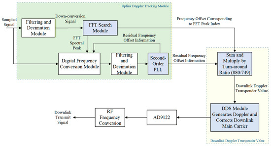
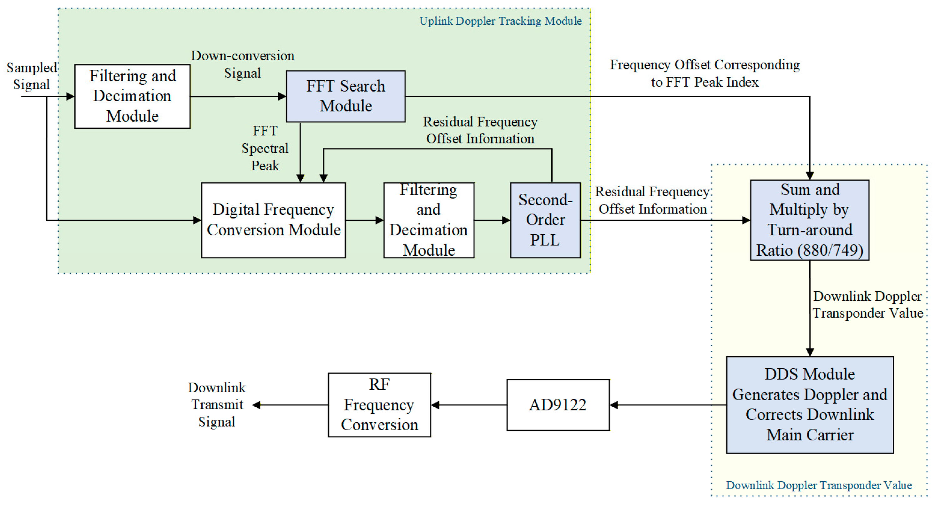
The UXB transponder system is primarily divided into two modules: the uplink Doppler tracking module and the downlink Doppler forwarding module. The overall signal processing flow is illustrated in Figure 1.
Figure 1.
UXB transponder signal processing flow.
As shown in Figure 1, the received ADC output signal undergoes an additional down-conversion stage to prevent aliasing before being fed into the carrier acquisition module. Prior to carrier acquisition, a coarse estimation is performed to locate the approximate spectral peak of the main carrier signal, which is then passed to the carrier tracking loop for precise acquisition.
The uplink output Doppler frequency word is then directly fed into the downlink Doppler forwarding module. The frequency word is multiplied by the turnaround ratio and integrated to convert the frequency information into phase information. Following compensation for frequency offset errors introduced by components such as the hardware imperfections of the AD9122, the resulting signal is input into a DDS to generate a signal at the corresponding frequency. This signal is then sent to a DA converter; undergoes frequency conversion, specifically RF frequency conversion; and is transmitted as the downlink signal. This downlink signal is used to verify the frequency offset error generated by the receiver’s signal processing chain.
2.2. Coherence Analysis
Prior to establishing a two-way communication link, it is essential to ensure frequency and phase coherence between the transmitter and receiver. This coherence is fundamental to achieving high-precision Doppler velocity measurement and reliable data transmission. Consequently, a system-level coherence analysis is a prerequisite.
Specifically, the system utilizes a shared onboard master oscillator (e.g., a 10 MHz crystal oscillator) to provide a unified timing reference for the entire transceiver signal chain. The Doppler frequency offset estimated in the uplink is not simply canceled; instead, it serves as a critical observation and is precisely mapped to the downlink transmission frequency via a fixed turnaround ratio. This coherent architecture enables the ground station to accurately derive the spacecraft’s radial velocity by comparing the frequencies of the up- and downlink signals.
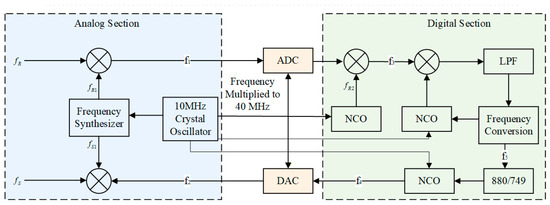
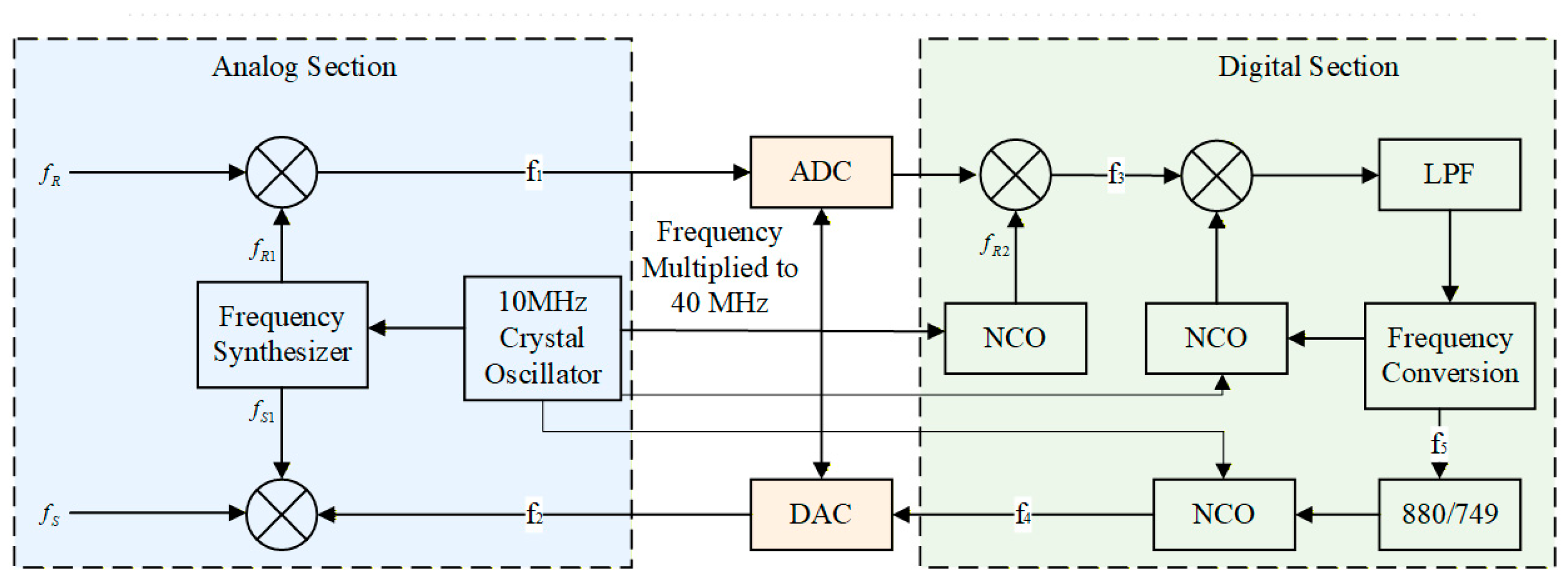
The proposed system employs rigorous clock synchronization and high-resolution phase accumulation to ensure that the locally generated compensation signal remains strictly coherent with the received signal. A schematic diagram illustrating the frequency flow throughout the up- and downlink carrier processing is presented in Figure 2.
Figure 2.
Transponder frequency plan.
The ground station’s base clock frequency is denoted as , and the frequency unit for Doppler measurement as . Then, the uplink frequency can be expressed as , and the ideal downlink transmission frequency is .
Taking into account the analog-to-digital conversion in the transponder, to simplify the analysis, the onboard clock is assumed to be accurate. The satellite’s base clock frequency is given by (generated equivalently from a 10 MHz crystal oscillator). The clock offset between the satellite and ground is denoted as .
The uplink signal received by the transponder first undergoes analog down-conversion with a conversion frequency of
The signal is then down-converted to an intermediate frequency (IF), followed by IF sampling to obtain a baseband digital signal for subsequent digital processing. First, a fixed down-conversion with frequency is applied, yielding a residual frequency that includes both Doppler shift and clock offset information. This residual frequency is then transformed according to the uplink–downlink frequency ratio to derive the downlink Doppler shift. After digital-to-analog conversion (DAC) to frequency , the signal is up-converted to the desired transmission frequency (up-conversion frequency ).
Throughout this process, the transponder’s frequency source consistently originates from a single 10 MHz crystal oscillator. The two up-conversion stages in the uplink receiver, and , are designed such that their nominal combined frequency is 0. In the downlink transmitter, the RF up-converter and the post-DAC frequency jointly ensure that the nominal output frequency is . Thus, the frequencies and are, respectively,
The recovered uplink carrier frequency is directly multiplied by the transponder ratio to obtain the downlink forwarding frequency, as follows:
The final output signal frequency is
Thus, the system design ensures coherence between the transmitted and received carrier frequencies.
Because the transceiver carriers are generated using carrier frequency words and scaling factors to maintain coherence, and considering the free-running phase of the digital-domain transceiver NCOs, the initial phase of the up- and downlink carriers in the transponder remains constant within each uplink synchronization cycle. However, the initial phase may vary across different synchronization cycles.
2.3. Carrier Synchronization Scheme
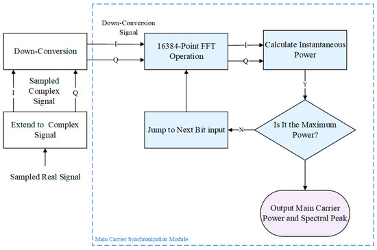
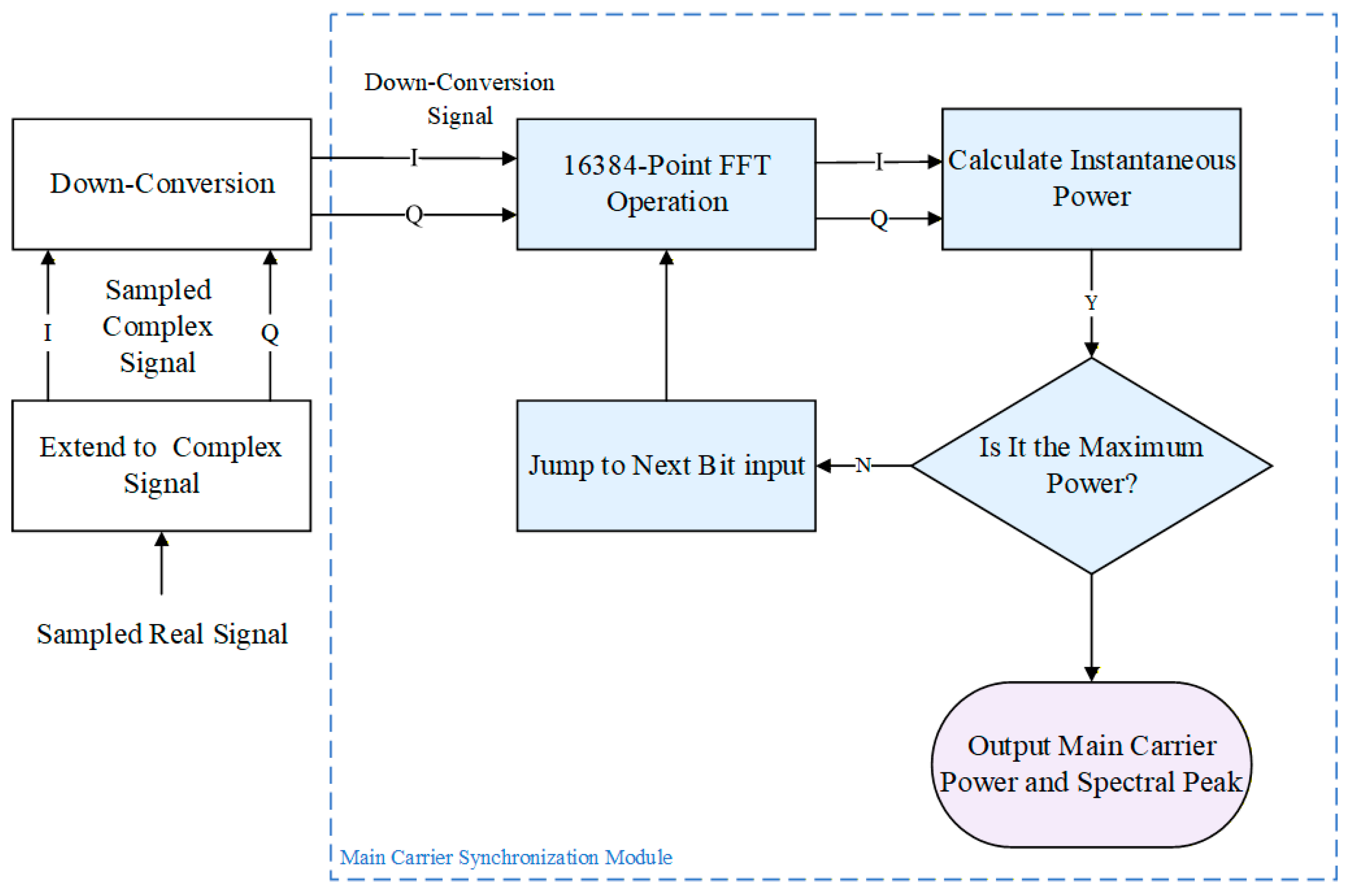
To ensure coherent demodulation and forwarding while meeting acceptable error limits, the receiver must perform carrier synchronization. The initial step in carrier synchronization involves coarse Doppler carrier tracking using FFT to locate the approximate position of the main carrier. The main process flow is illustrated in Figure 3.
Figure 3.
FFT-based carrier acquisition flow.
Prior to acquisition, carrier pre-estimation is performed to define the tracking range and improve system efficiency. The spectral bin containing the Doppler frequency offset can be determined based on detection and estimation theory. The system requires a tracking range of ±450 kHz. Therefore, the signal bandwidth configured in the FFT coarse acquisition module is approximately 900 kHz. After down-conversion, the input signal is fed into the FFT, which has a frequency resolution of 76.28 Hz. Consequently, the search range spans from approximately −625 kHz to +625 kHz, centered on the nominal received frequency ().
Considering frequency drift rates of 3 kHz/s and 15 kHz/s, the FFT point size is set to 16,384. Thus, the acquisition window of the FFT-based coarse frequency estimator is approximately 13 ms. Within this extremely short duration, the Doppler variation is negligible—remaining less than 0.2 Hz even at the maximum drift rate of 15 kHz/s. Consequently, the received signal can be treated as having a static Doppler shift during acquisition. This aligns with the fundamental design principle of carrier synchronization receivers, where the acquisition stage must operate under quasi-static conditions to ensure reliable frequency estimation before fine tracking.
Once the FFT index is obtained, the corresponding frequency offset value is latched and passed to the carrier tracking unit. A control signal is then generated to indicate the completion of coarse frequency offset estimation, initiating the carrier tracking loop for closed-loop tracking.
Following coarse acquisition, a PLL is employed to achieve more precise synchronization and tracking of the carrier frequency and phase, thereby enabling coherent demodulation of the main carrier. The system designed in this study utilizes a digital Costas loop for fine acquisition and tracking of the carrier frequency offset.
In the analog domain, an ideal integrator-based active filter serves as the loop filter, forming a Type II second-order analog loop. We define the natural angular frequency and the damping ratio as follows:
where is the loop gain, and and are time constants related to resistance and inductance. The closed-loop transfer function of the loop can then be expressed as
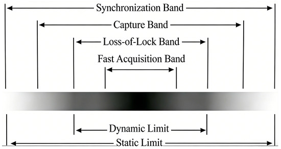
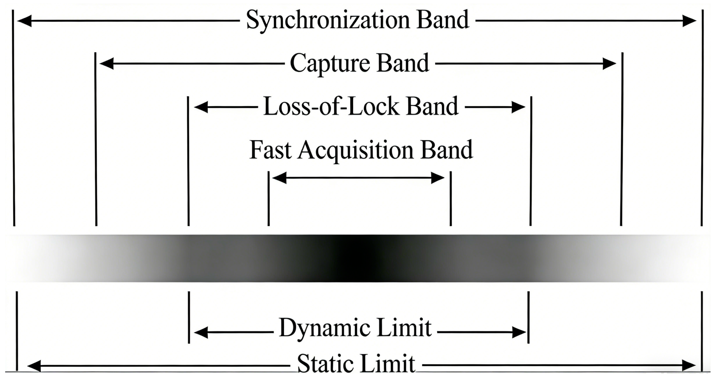
Another critical characteristic of the loop is its frequency band characteristics. The relationship for the PLL acquisition range is illustrated in Figure 4. Since the coarse FFT frequency offset estimation is already close to the actual offset, the initial frequency difference between the PLL designed in this study and the input signal can be assumed to fall within the fast acquisition range when phase tracking begins.
Figure 4.
Schematic of PLL frequency band characteristics.
After completing the parameter design in the analog domain, it is necessary to convert these parameters into their digital-domain equivalents suitable for the corresponding digital circuit architecture. The system can be transformed from the analog to the digital domain using the following bilinear transformation:
where .Evidently, the z-domain transfer function expressed above can be implemented digitally using scaling and integrator elements.
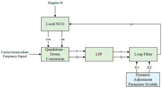
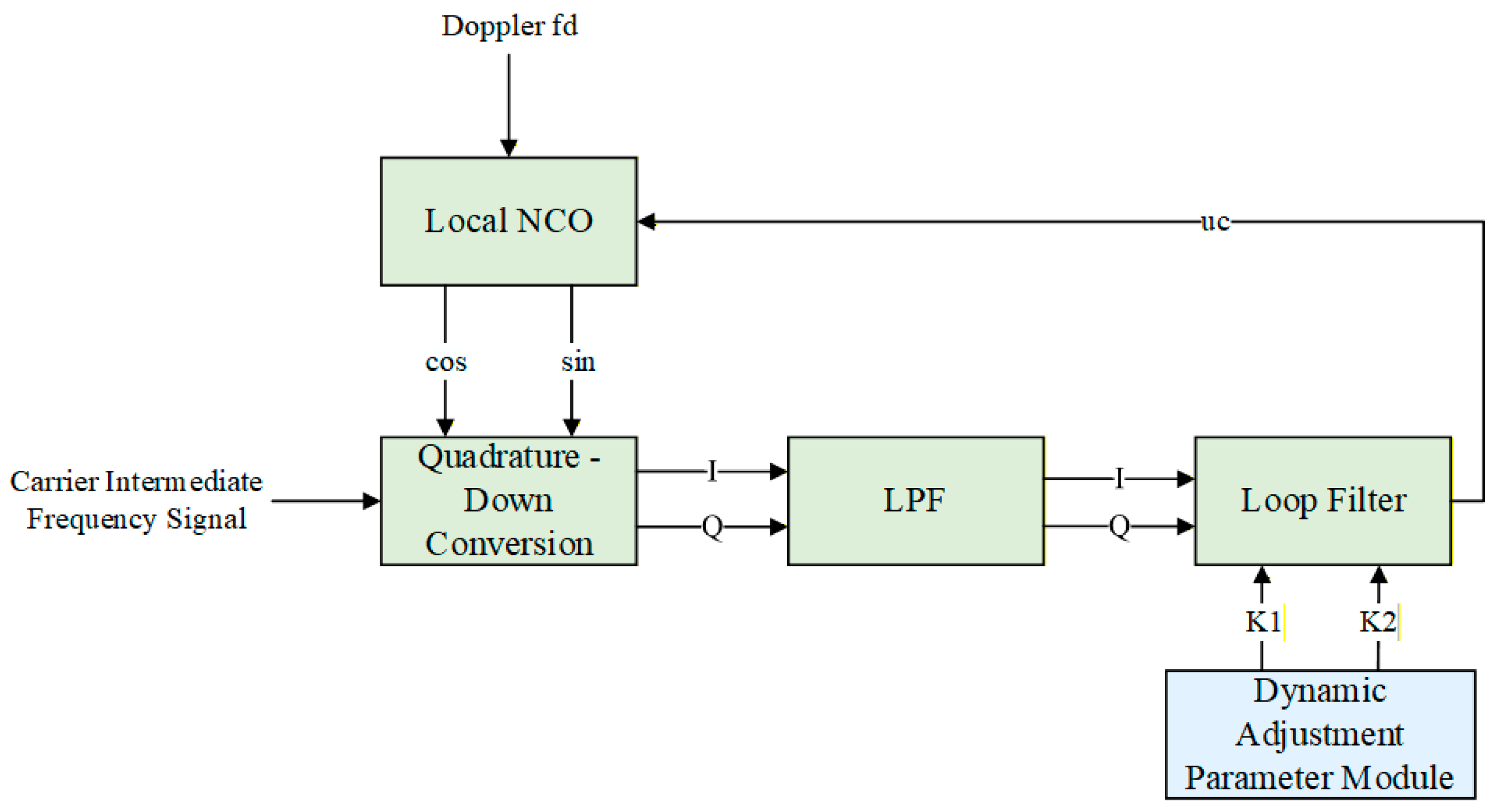
Figure 5 illustrates the internal operating structure of the PLL. The carrier tracking loop first performs quadrature down-conversion on the input signal. The resulting complex signal is then low-pass-filtered, isolating the near-DC baseband components. Concurrently, a dynamic parameter adjustment module is designed outside the main PLL block. This module dynamically adjusts the loop filter parameters and based on the signal state and SNR. The system identifies varying SNR conditions and adapts; in particular, under low SNR, the PLL parameters are reduced to narrow the loop bandwidth, thereby enhancing noise immunity and ensuring stable operation within the convergence region without loss of lock.
Figure 5.
Carrier tracking PLL structure.
Since PM is employed, the spectrum of the modulated signal contains a discrete carrier component (also known as a residual carrier). This allows the quadrature (Q) channel of the carrier to be sampled directly, yielding a sinusoidal phase detector characteristic. However, a loop with a sinusoidal phase detector is susceptible to the “hang-up” phenomenon, which can prolong acquisition time and theoretically lead to infinite acquisition in certain cases. To mitigate this, an FFT module is introduced to provide a coarse estimate of the Doppler frequency offset . This estimate, combined with the phase error output from the loop filter, serves as the frequency word input to the local NCO.
With the assistance of this frequency offset pre-estimation, the carrier frequency difference entering the loop filter becomes very small, ensuring it falls directly within the PLL’s fast acquisition range. This enables the PLL to rapidly complete both frequency and phase acquisition, thereby effectively avoiding the hang-up phenomenon.
3. Error Analysis
In this section, we establish the overall error model for the system, analyzing the sources that contribute to frequency offset error within the transponder in detail.
3.1. System Digitalization Errors
In FPGA-based digital processing, the system inherently carries a series of deviations caused by quantization and phase jitter. These errors introduce slight nonlinear biases into the frequency/phase information transmission chain and disrupt the strict proportional frequency relationship between the downlink and uplink signals, thereby compromising coherence and ultimately degrading velocity measurement accuracy.
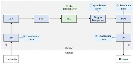
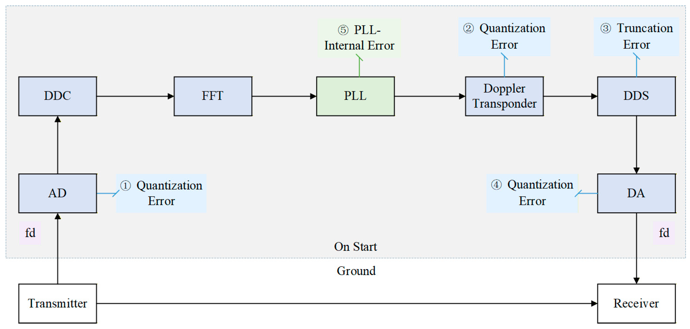
Figure 6 shows the error model, which essentially quantifies the degree to which quantization errors impair system coherence. We can analyze these errors individually as follows:
Figure 6.
System error sources.
- Quantization Error in the Down-Conversion Stage (Error ①):In Doppler compensation systems, DDS is often used to generate the required carrier for down-conversion. The core of a DDS is the phase accumulator. Its frequency resolution is given bywhere is the sampling frequency and is the bit width of the frequency control word (FCW). Since the actual down-conversion frequency required for communication is arbitrary and rarely an integer multiple of this resolution, quantization error is introduced:The quantization error is an absolute error that causes a deviation between the DDS-generated carrier frequency and the ideal down-conversion frequency, leading to an offset in the down-converted signal’s frequency and affecting the accuracy of subsequent signal processing.
- Turnaround Ratio Quantization Error (Error ②):During downlink Doppler forwarding, multiplication by the fixed UXB turnaround ratio is required. Since an FPGA can only accept integer inputs, quantization (truncation) of this turnaround ratio introduces an error:where denotes the floor function, bringing about truncation errors, and represents the clock multiplier ratio between the carrier synchronization module and the Doppler forwarding module. The magnitude of this error in typical engineering applications is approximately . From a communication system performance perspective, an error of this negligible magnitude can be approximately ignored.
- Frequency Resolution Error in Phase Accumulation (Error ③):The n-th cycle phase signal in the phase accumulation stage iswhere is the accumulated frequency. When the frequency word is accumulated to form a phase, precision errors may arise. If the actual Doppler frequency cannot be precisely represented as an integer multiple of the resolution, a residual frequency bias of exists with each accumulation. Over time, these residual biases accumulate, leading to a deviation in the total accumulated phase.
- Quantization Error in the DA Internal Frequency Conversion (Error ④):Similarly to Error ①, Equation (10) shows the quantization error in the DA stage. This error is deterministic and can be calculated and compensated for before the forwarding stage.
3.2. PLL Errors
Since the sources of error within the PLL differ from those above, particularly with more quantization error, we conduct an in-depth analysis of the impact of the loop filter parameters on the dynamic performance and steady-state error of the loop, based on the digital PLL model established in Section 2.
By controlling the coupling relationship through and , Equation (7) can be rewritten as
Then, the error transfer function for this system is given by
Given that the PLL input-modulated signal input into the PLL from the receiver is , the final value theorem yields that the phase error is
where , which contains both the main carrier frequency component and each subcarrier frequency component. Substituting this expression into the final one yields that the system’s steady-state phase error is . Preliminary derivation indicates that, for signals under BPSK-PM modulation, the static error of this loop is zero. However, in practical signal acquisition, issues such as dynamic error and mean jitter can arise due to dynamic frequency offsets. We now proceed to analyze the internal dynamic error of the PLL in detail.
First, within the loop model, analyzing the dynamic frequency problem requires a key parameter: the loop bandwidth. The loop bandwidth, defined as the equivalent noise bandwidth of the system function, is expressed as [24]
The loop equivalent bandwidth describes the loop’s ability to filter out noise, and the loop is directly related to , expressed as
where and represent the front-end bandwidth and input signal-to-noise ratio of the input signal, respectively. This formula indicates that by designing a loop bandwidth significantly smaller than the front-end bandwidth, the internal signal-to-noise ratio of the loop can be substantially enhanced, meaning its noise suppression capability becomes stronger.
As shown, the phase noise generated within the PLL is directly related to the loop bandwidth. Specifically, when Gaussian white noise with a constant power spectral density of is applied as an equivalent input phase noise and filtered by a loop with a power response of , the output phase noise power equals the phase noise power output from a rectangular filter with a bandwidth of and a power response of . This relationship is given by [25]
When the white noise power spectral density is
Equation (19) can be rewritten as
where . It can be observed that a smaller results in stronger suppression of white noise passing through the loop. However, is also related to the system’s dynamic tracking capability. The steady-state error due to a frequency ramp is inversely proportional to . Therefore, a narrower bandwidth leads to poorer dynamic tracking performance. In the UXB system, the Doppler shift is static, allowing the PLL to operate effectively with a narrow bandwidth.
Furthermore, for BPSK-PM signals, in addition to additive white Gaussian noise in the channel, there exists an inherent source of interference: modulation self-noise. Random transitions of the data bits generate noise at the phase detector output, which is correlated with the signal power and has a broadband power spectrum. The relationship between this type of noise and the loop bandwidth is expressed as
In addition to the phase noise errors primarily governed by the loop bandwidth mentioned above, finite word-length effects in digital systems also introduce low-level truncation errors and quantization noise. In the NCO phase accumulator, when using the higher-order M bits from an N-bit width for look-up table addressing, a step size of bits is discarded, resulting in phase truncation. The quantized phase step can be expressed as
The variance of the truncation error over one phase period can be written as
Since this noise is generated internally within the loop, according to [26], the variance of the final output truncation error is approximately
where represents the proportion of power within the loop bandwidth. This noise may result in a periodic sawtooth-shaped error between the ideal phase value and the actual generated phase value.
Simultaneously, quantization error also exists within the loop filter, as the loop filter executes the operation
where the control parameters and are on the order of approximately 0.0001, and the FPGA’s quantization leads to parameter errors, causing rounding errors around 0.1 mHz. This affects the loop filter’s damping ratio and oscillation frequency. Therefore, integrator rounding errors may prevent the loop from becoming completely stationary when locked, instead inducing sustained low-level periodic jitter around the equilibrium point, known as limit cycle oscillation. This phenomenon can cause the calculated average phase error of the PLL to shift.
4. Simulation Results
In this section, based on the analysis of the error model presented above, we conduct practical modeling and simulations to accurately assess the impact of these errors.
4.1. Full-Link Simulation
In the actual system, we input a signal sampled at 40 MHz, using clock frequencies of 40 MHz and 120 MHz to control the receiver. Initially, a 32-bit quantization scheme was employed for processing. However, repeated tests revealed that it failed to meet the high-precision velocity measurement requirements. Consequently, an optimized scheme using 48-bit quantization was proposed. To validate the theoretical model and assess the effectiveness of this optimization, a complete MATLAB simulation system (R2024b, MathWorks, Inc., Natick, MA, USA) was constructed, encompassing ground uplink signal transmission, onboard satellite reception and processing, and downlink retransmission.
The detailed simulation parameters are listed in Table 1.
Table 1.
Simulation parameters and conditions.
The simulation strictly adheres to the architecture shown in Figure 1 and employs the carrier synchronization scheme described in Section 2.
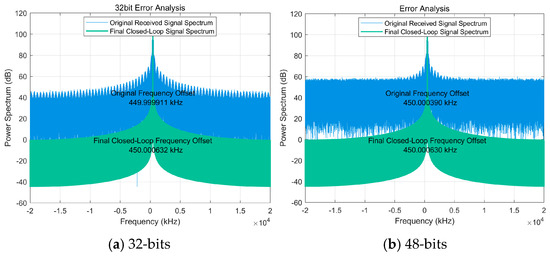
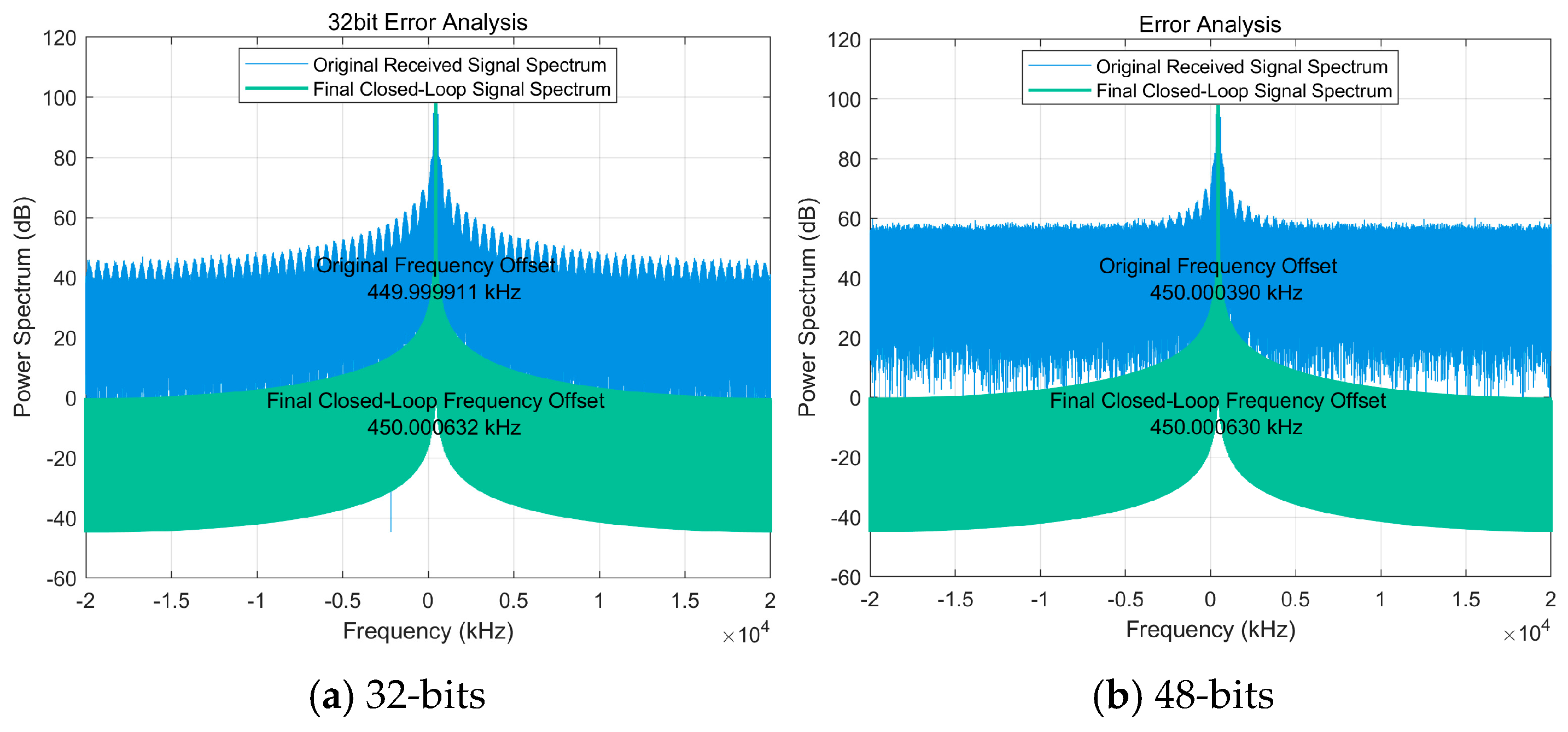
Figure 7 presents the frequency offset output from the system under the 32- and 48-bit quantization schemes for a single run. It can be observed that, with 32-bit quantization, the frequency offset error is 0.7201 Hz. In contrast, under the 48-bit quantization scheme, the error is reduced to 0.0073 Hz. It shows that the error magnitude for the 48-bit scheme is significantly smaller, indicating preliminarily superior system performance.
Figure 7.
Frequency offset error output from the system.
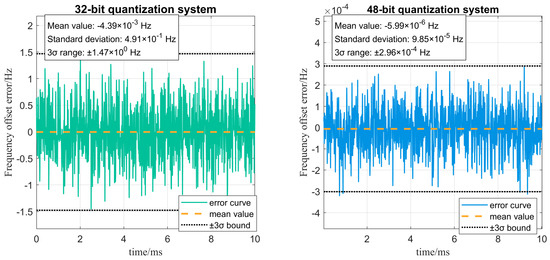
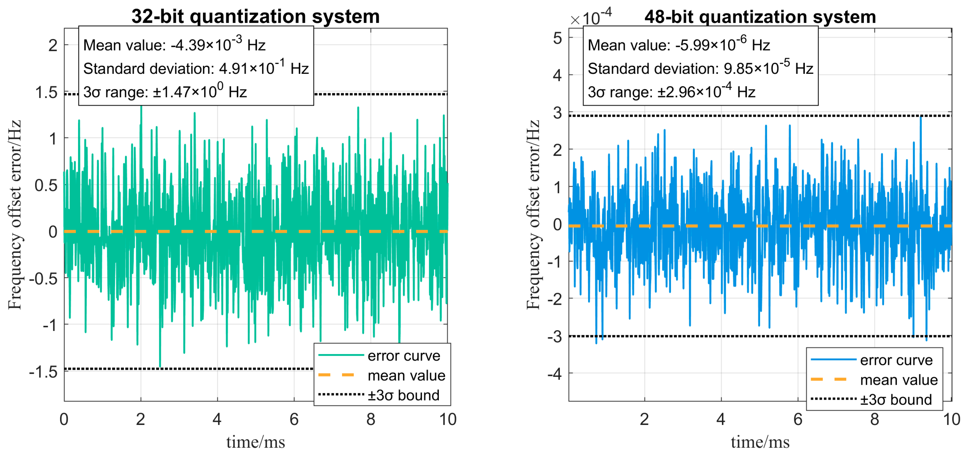
Figure 8 presents a time-domain comparison of the frequency offset error output from the system under the 32- and 48-bit quantization schemes. Visually, the frequency offset error of the 32-bit system fluctuates within a range of approximately ±1.5 Hz and exhibits a noticeable steady-state bias. In contrast, the error amplitude of the optimized 48-bit system is compressed to within ±0.000001 Hz, showing significantly reduced fluctuations. A quantitative comparison reveals that the 48-bit optimization scheme reduces the system’s frequency offset error by approximately six orders of magnitude, providing preliminary validation of the significant effectiveness of bit-width extension in enhancing system coherence.
Figure 8.
Statistical comparison.
4.2. PLL Performance Simulation
As the core of carrier synchronization, the parameter settings of the PLL directly affect the system’s error characteristics. To determine the optimal operating point, the system was tested with multiple sets of and .
As can be observed from Table 2, when is reduced from 25 to the sub- level, the standard deviation sharply decreases from 330.38 to below approximately 10. This demonstrates that reducing can effectively minimize phase jitter error. When , the standard deviation stabilizes within the relatively low range of 6.32 to 12.56. However, when becomes excessively small, dropping to the level, the standard deviation approaches zero, yet the mean error stabilizes at −18.8 Hz.
Table 2.
System error statistics.
We can summarize the dynamic balance performance of the PLL as follows: when is relatively large and is substantial, the system exhibits strong dynamic tracking capability (small steady-state error) but poor noise performance (large variance). Conversely, when both and are relatively small, the system’s dynamic tracking capability weakens (larger steady-state error), but it becomes more effective at suppressing jitter (small variance).
As a result, the total error caused by internal phase jitter in the PLL can be expressed as
Based on the data presented in Table 1, we selected the parameters , which demonstrate favorable loop performance. This yields the loop phase noise for , as summarized in Table 3.
Table 3.
PLL Phase Error Analysis.
The conversion formula between phase variance and frequency variance is
Typically, the boundary is taken as the peak frequency deviation range:
Therefore, the dynamic error caused by phase jitter within the PLL translates to an error range of approximately ±1.23 × 10⁻⁵ Hz.
4.3. Validation of the Optimization Scheme
To further conduct a system-level assessment, the frequency offset error was mapped to the velocity measurement error. Under the 48-bit quantization scheme, the standard deviation of the system’s velocity measurement error is below 0.01 mm/s, significantly superior to the several mm/s observed with the 32-bit quantization. This demonstrates that the proposed optimization scheme not only enhances frequency coherence but also directly ensures the system’s high-precision requirements for Doppler-based velocity measurement.
Table 4 presents the overall performance metrics. The significant systematic frequency offset error in the 32-bit system severely degrades the frequency coherence between the transmitted and received signals. In contrast, the 48-bit system suppresses this type of error to a negligible level, with all metrics meeting the design requirements derived from the CCSDS [1] standards and established engineering practices. Although the 48-bit scheme increases logic resource consumption by approximately 45–55%—primarily affecting registers, lookup tables, and DSP blocks—this overhead is fully acceptable on modern space-qualified FPGA platforms such as Xilinx Virtex UltraScale+ or Microchip RTG4, ensuring excellent engineering feasibility while effectively safeguarding the coherent retransmission mechanism of the UXB system.
Table 4.
32-Bit vs. 48-Bit System Performance.
In summary, the 48-bit optimization scheme theoretically enhances system performance to over five times the required specifications. Practical simulations also demonstrate an order-of-magnitude improvement, validating its effectiveness and necessity for high-precision deep-space telemetry, tracking, and command applications.
4.4. Systematic Error Decomposition
Based on the preceding error analysis and simulation results, to gain a deeper understanding of the optimization mechanism, we begin with a theoretical analysis. According to the analysis in Section 2.3, the Doppler shifts captured by the system can all be considered static. Assuming the Doppler frequency offset input into the receiver is , the quantized frequency word output by the PLL is
According to the UXB system specification, the transceiver frequency ratio is . Consequently, the onboard retransmission ratio is , and the ground retransmission ratio is . The quantized onboard retransmission ratio is given by
To verify the closed-loop frequency offset, we directly feed the quantized frequency word, after PLL compensation, into the retransmission module. It is then multiplied by the quantized retransmission ratio, yielding the updated retransmission frequency word:
Finally, this frequency word is input into the DDS. Based on the DDS frequency formula, the signal frequency retransmitted to the ground station in the downlink is
Substituting the 32-bit quantization parameters yields a systematic theoretical error of 0.96000074 Hz. In contrast, employing 48-bit quantization reduces the systematic theoretical error to merely 0.00000083 Hz.
Table 5 presents the system-level quantization error budget. In the 32-bit system, the phase accumulator frequency resolution error (0.011 Hz), the internal DAC DDS quantization error, and the down-conversion DDS error (7.451 × 10⁻⁴ Hz) are evidently the primary contributors, with magnitudes of the same order, while the retransmission quantization error is negligible. After extending the bit width to 48 bits, all frequency-resolution-based errors are reduced.
Table 5.
Systematic Error Decomposition Budget.
The actual reduction magnitude reaches an order of 105. For example, the phase accumulator error decreases from 0.011 Hz to 1.68 × 10⁻⁷ Hz.
Comparing the budget in the table with the result given by Equation (32), it can be seen that the theoretical error is larger than the decomposed budget. This is because the theoretical calculation represents the theoretical worst-case scenario, encompassing all possible error amplification mechanisms. In contrast, the value of 1.25 × 10⁻² Hz in Table 5 is a simple sum of the independent worst-case values for each component, without considering error propagation. From the perspective of design margin, the more conservative theoretical value should be adopted as the system specification. The actual simulation result (±0.5 Hz) lies between these two values, validating the reasonableness of the theoretical model. It also indicates that the actual system performance is better than the theoretical worst-case scenario, retaining sufficient design margin.
Following the 48-bit optimization, the primary limitation to system accuracy shifts from quantization-induced systematic errors to the stochastic phase jitter governed by the PLL bandwidth. This indicates that, for future performance gains beyond the achieved level, research should focus on optimizing the PLL’s noise performance, for instance, through adaptive loop bandwidth control strategies.
5. Conclusions
In this paper, we focus on the UXB satellite telemetry, tracking, and command (TT&C) system, conducting an in-depth analysis and optimization of the system performance limitations caused by quantization errors in its digital implementation. The research identifies that the finite word-length effect is the core factor degrading the coherence between transmitted and received signals and constraining the Doppler velocity measurement accuracy within the carrier synchronization and Doppler retransmission link.
Through theoretical modeling, this work systematically analyzes the sources of error and their magnitude of impact. The primary analysis covers both stochastic and systematic errors related to the PLL bandwidth. The phase accumulator resolution error and the internal DDS quantization error of the digital-to-analog converter are identified as the main contributors, with comparable magnitudes. The down-conversion DDS error follows in significance, while the retransmission ratio quantization error is negligible. The random jitter within the PLL is categorized as a stochastic error, independent of bit width and solely governed by the loop bandwidth.
The analysis demonstrates that when employing the conventional 32-bit quantization scheme, the system incurs a frequency offset error of approximately 0.96 Hz, which fails to meet the requirements for high-precision velocity measurement. Therefore, extending the bit width to 48 bits reduces all frequency-resolution-based errors by a factor of approximately 216, with the actual reduction magnitude reaching an order of 108. The corresponding velocity measurement error is better than 0.01 mm/s. This result significantly exceeds the system specifications, strongly validating the effectiveness and necessity of the proposed scheme for high-precision deep-space TT&C applications.
Future work may focus on investigating adaptive loop bandwidth control strategies to optimize the PLL’s tracking performance and noise suppression capability under dynamic channel conditions, thereby enhancing the system’s robustness in complex environments.
Author Contributions
Conceptualization, J.Z.; methodology, H.Z. and Z.S.; software, M.W.; validation, G.L., W.Z. and J.Z.; formal analysis, H.Z.; investigation, Z.S.; writing—original draft preparation, H.Z.; writing—review and editing, Z.S.; supervision, G.L. and J.Z. All authors have read and agreed to the published version of the manuscript.
Funding
This research received no external funding.
Data Availability Statement
Data is contained within the article.
Acknowledgments
The authors thank the Editors and the anonymous Referees for their instructive comments.
Conflicts of Interest
The authors declare no conflicts of interest.
References
- CCSDS. Radio Frequency and Modulation Systems—Part 1: Earth Stations and Spacecraft. In CCSDS 401.0-B-32 (Blue Book); CCSDS: Washington, DC, USA, 2021. [Google Scholar]
- Li, M.; Zhang, Y.; Kong, J.; Huang, X.; Shi, K.; Guo, G.; Xue, N. Delay-Adaptive Federated Filtering with Online Model Calibration for Deep-Space Multi-Spacecraft Orbit Determination. Aerospace 2026, 13, 160. [Google Scholar] [CrossRef] [Scilit]
- Han, Y.; Fu, Y.; Bai, W.; Gong, X. Error Source Analysis of Atmospheric Occultation Sounding System. Chin. J. Space Sci. 2017, 37, 724–728. [Google Scholar] [CrossRef] [Scilit]
- Ding, W.; Zhang, Z.; Yang, H.; Chen, F. Analysis of Line-of-sight Measurement Error for Satellite-borne Observation Platform. Chin. J. Space Sci. 2017, 37, 238–248. [Google Scholar] [CrossRef] [Scilit]
- Li, L. Safety assessment of satellite communication links for large fixed-wing UAS. In Proceedings of the 2024 IEEE 6th International Conference on Civil Aviation Safety and Information Technology (ICCASIT), Hangzhou, China, 23–25 October 2024; pp. 487–490. [Google Scholar]
- Shi, L.; Luo, Q.; Dou, J.; Li, Q. Research on Adaptive Communication Method of Inter-satellite Link in Satellite Group System. In Proceedings of the 2024 7th International Conference on Electronics Technology (ICET), Chengdu, China, 17–20 May 2024; pp. 822–827. [Google Scholar]
- Ekici, E.; Akyildiz, I.F.; Bender, M.D. A distributed routing algorithm for datagram traffic in LEO satellite networks. IEEE/ACM Trans. Netw. 2001, 9, 137–147. [Google Scholar] [CrossRef] [Scilit]
- Maurice, M.; Stallard, M. Distributed satellite missions and technologies—The TechSat 21 program. In Proceedings of the Space Technology Conference and Exposition, Albuquerque, NM, USA, 28–30 September 1999; pp. 1–8. [Google Scholar]
- Gopalam, S.; Collings, I.B.; Hanly, S.V.; Inaltekin, H.; Pillai, S.R.B.; Whiting, P. Zak-otfs implementation via time and frequency windowing. IEEE Trans. Commun. 2024, 72, 3873–3889. [Google Scholar] [CrossRef] [Scilit]
- Lin, H.; Yuan, J. Orthogonal delay-doppler division multiplexing modulation. IEEE Trans. Wirel. Commun. 2022, 21, 11024–11037. [Google Scholar] [CrossRef] [Scilit]
- Liu, Y.; Pan, C.; Gong, T.; Wang, Y.; Chen, M. Delay-Doppler Diversity Analysis of Oddm Modulation in Satellite Communication Systems. 2025. Available online: https://arxiv.org/abs/2506.19688 (accessed on 24 March 2026).
- Tong, J.; Yuan, J.; Lin, H.; Xi, J. Orthogonal delay-doppler division multiplexing (oddm) over general physical channels. IEEE Trans. Commun. 2024, 72, 7938–7953. [Google Scholar] [CrossRef] [Scilit]
- Berner, J.B.; Kayalar, S.; Perret, J.D. The NASA spacecraft transponding modem. In Proceedings of the IEEE Aerospace Conference, Big Sky, MT, USA, 19–25 March 2000; Volume 7, pp. 195–209. [Google Scholar]
- Ren, B.; Liu, J.; Li, Z.; Wu, J.; Yao, Z. Satellite requirement preference driven TT&C resources scheduling algorithm for time sensitive missions. In Proceedings of the IEEE 3rd International Conference on Electronic Information and Communication Technology (ICEICT), Shenzhen, China, 13–15 November 2020; pp. 15–19. [Google Scholar]
- Preetha, S.B.K.; Sai, J.V.M.; Raj, V.S.; Sekhar, M.J.; Lavanya, R. Anomaly Detection in Satellite Power System using Deep Learning. In Proceedings of the 2024 IEEE International Conference on Electronics, Computing and Communication Technologies (CONECCT), Bangalore, India, 12–14 July 2024; pp. 1–5. [Google Scholar]
- Salim, S.; Moustafa, N.; Reisslein, M. Cybersecurity of Satellite Communications Systems: A Comprehensive Survey of the Space, Ground, and Links Segments. IEEE Commun. Surv. Tutor. 2025, 27, 372–425. [Google Scholar] [CrossRef] [Scilit]
- Werner, L.; Liman, C.; Gardill, M. High-Fidelity Simulation of a Pico Satellite Link. In Proceedings of the 2022 IEEE Space Hardware and Radio Conference (SHaRC), Las Vegas, NV, USA, 16–19 January 2022; pp. 7–10. [Google Scholar]
- Langton, M.T.; Yang, Z.; Pan, G.; Zhang, H.; Luo, G.; Yang, H. Security Challenges in Satellite Ground Stations and their Risk Mitigation Techniques. In Proceedings of the 2024 13th International Conference on Communications, Circuits and Systems (ICCCAS), Xiamen, China, 10–12 May 2024; pp. 508–513. [Google Scholar]
- Xu, Y.; Jiao, Y.; Pan, X.; Wang, J.; Zhou, H.; Cao, J. An efficient scheduling method for satellite TT&C resources. In Proceedings of the 7th International Conference on Big Data and Information Analytics (BigDIA), Chongqing, China, 29–31 October 2021; pp. 340–349. [Google Scholar]
- Yang, Y.; Han, M.; Feng, Z.; Fan, H.; Bai, J. Design and realization of a novel multitask TT&C operation pattern. J. Syst. Eng. Electron. 2008, 19, 1243–1249. [Google Scholar] [CrossRef] [Scilit]
- Smith, S.W. Digital Signal Processing: A Practical Guide for Engineers and Scientists, 1st ed.; Newnes: Burlington, MA, USA, 2003. [Google Scholar]
- Wang, C.; Yu, H.; Wang, J.; Liu, T. Bias Analysis of Parameter Estimator Based on Gauss-Newton Method Applied to Ultra-Wideband Positioning. Appl. Sci. 2020, 10, 273. [Google Scholar] [CrossRef] [Scilit]
- Karlgaard, C.D.; Lugo, R.A.; Shidner, J.D.; Hines, G.D.; Amzajerdian, F.; Gragossian, A.; Litton, D.K.; Angster, S.R. Navigation Doppler Lidar Performance Assessment and Trajectory Reconstruction of the Intuitive Machines IM-1 Lunar Landing. In Proceedings of the AAS Guidance, Navigation and Control Conference, AAS 25-036, Breckenridge, CO, USA, 31 January–5 February 2025. [Google Scholar]
- Best, R.E. Phase-Locked Loops: Design, Simulation, and Applications, 6th ed.; McGraw-Hill: Columbus, OH, USA, 2007. [Google Scholar]
- Gardner, F.M. Phaselock Techniques, 3rd ed.; Wiley-Interscience: Hoboken, NJ, USA, 2005. [Google Scholar]
- Staszewski, R.B.; Balsara, P.T. All-Digital Frequency Synthesizer in Deep-Submicron CMOS; Wiley-Interscience: Hoboken, NJ, USA, 2006. [Google Scholar]

Disclaimer/Publisher’s Note: The statements, opinions and data contained in all publications are solely those of the individual author(s) and contributor(s) and not of MDPI and/or the editor(s). MDPI and/or the editor(s) disclaim responsibility for any injury to people or property resulting from any ideas, methods, instructions or products referred to in the content. |
© 2026 by the authors. Licensee MDPI, Basel, Switzerland. This article is an open access article distributed under the terms and conditions of the Creative Commons Attribution (CC BY) license.