


Abstract
This paper presents an ultra-miniaturized and high-quality factor embedded loaded coaxial substrate integrated waveguide (ELCSIW) filter. Integrating a substrate-integrated coaxial resonator with a capacitively loaded air cavity achieves a 99% reduction in size compared to a conventional SIW cavity. Incorporating an air gap in the capacitive loading structure significantly enhances the resonator’s quality factor. A comprehensive analysis of the miniaturization factor and quality factor in relation to cavity structure dimensions is performed. Guidelines for fabricating the highly loaded cavity are presented. To demonstrate the benefits of this technique, a two-pole band-pass filter with a 6.3% bandwidth at 1.1 GHz is designed, fabricated, and measured. The overall footprint of the filter is 10.5 mm × 20.5 mm, which is comparable to 0.07 × 0.14 . The measured insertion loss is 0.54 dB, and the upper band is spurious-free up to 7 times the resonant frequency. The exceptional performance and compactness of the loaded coaxial substrate integrated waveguide cavities highlight their immense potential for compact advanced wireless systems.
1. Introduction
Compact, high-performance, and cost-effective filters are becoming increasingly desirable due to advancements in wireless communication systems. Among the various technologies available, substrate integrated waveguide (SIW) has gained attention for its planar structure and relatively high-quality factor [1,2]. However, SIW filters typically occupy a larger footprint compared to coplanar waveguides and microstrip lines [3].
Various techniques have been developed to reduce the footprint of SIW filters, especially those operating at low microwave frequencies, to realize a more compact structure of SIW technology. Sub-mode techniques of SIW resonators have been proposed to minimize SIW cavities by cutting the cavity of the dominant mode at its symmetric imaginary magnetic walls [4,5,6,7,8,9,10,11]. For instance, half-mode and quarter-mode SIW resonators can achieve 50% and 75% size reduction, respectively [4,5]. In [9], sixteenth-mode and thirty-second mode cavities can achieve miniaturization of 93% and 96.8%, respectively. The drawback of this technology is that the unloaded quality factor () of these sub-modes is low due to increased radiation loss at the open edges. An alternative method for achieving miniaturization in SIW structures is through the folded waveguides technique [12,13,14,15]. In [14], a compact resonator with more than 70% footprint reduction and improved quality factor is achieved using a double-folded SIW technique. Similarly, the authors in [15] propose a quadruple-folded SIW cavity, demonstrating an 89% reduction in footprint for an SIW resonator. Unlike sub-modes, the folding waveguides technique offers an advantage in terms of quality factors due to the absence of open edges. However, this technique has limitations in terms of the number of folds and the achievable quality factors, due to additional losses introduced with each fold. Composite right/left handed (CRLH) resonators have been proposed in SIW technology to reduce the size of the SIW structure [16,17,18]. The CRLH structure is realized by series and shunt capacitance and inductance that exhibit a negative refractive index, allowing resonance below the cavity’s cutoff frequency [16]. In [16,17], SIW resonators based on CRLH loading achieve miniaturization factors of 45% and 80%, respectively, with the higher reduction obtained by combining CRLH loading with a folded SIW cavity. These designs exhibit lower than conventional SIW resonators due to the additional loading elements and discontinuities required for the CRLH response, which increase dielectric and conductor losses.
In [19,20,21,22,23,24], a highly capacitive loading technique for SIW resonators based on a coaxial SIW resonator was introduced. According to [19], a highly loaded evanescent-mode cavity is fabricated using Low-Temperature Co-fired Ceramics (LTCC). The evanescent-mode cavity is constructed by a single square post in the cavity’s center, where capacitive loading is established between the post’s upper surface and the top metallic layer. This structure achieves a of 700 with 89% miniaturization. The post structure, however, restricts the effective loading range that can be attained. In [20], an embedded coaxial SIW cavity is implemented using a multilayer LTCC structure. The inductive section of the coaxial resonator is created by central vias short-circuited to the ground plane, forming the inner conductor. A circular metal patch is placed under the top metal layer and electrically connected to the ground through the inner via, creating a capacitive gap characteristic of a combline configuration. This topology enables strong capacitive loading by increasing the patch diameter or reducing the dielectric substrate thickness between the patch and the top conductor. As a result, the loading capacitance is formed across a thin dielectric-filled substrate where the electric field is highly concentrated. This allows for a miniaturization factor of approximately 96.8%. However, the concentration of strong electric fields within a thin dielectric gap increases both dielectric and conductor losses, limiting the unloaded quality factor to 209. In [21], the authors introduce an evanescent-mode SIW cavity composed of two dielectric substrates and three metal layers with a circular metal patch embedded between the top and bottom cavity metal layers. The patch is short-circuited to the bottom wall through a central via ring forming a coaxial resonator that operates along the substrate normal direction. The resonance frequency is determined by the characteristic admittance of the short-circuited transmission line formed by the via ring fence and the capacitance between the patch and the cavity walls. Increasing the patch diameter, reducing the spacing between the patch and the top metal layer, or decreasing the via ring diameter increases the capacitive loading and enables a miniaturization factor of up to 96.4%. However, as the capacitive loading increases, both dielectric and conductor losses rise due to the strong electric field across the dielectric-filled gap, resulting in an unloaded quality factor of 325. The work in [22,23] present substrate-integrated evanescent-mode cavity filters based on heavily loaded cavities combined with piezoelectric actuation to enable frequency tuning. The resonator consists of a central capacitive ring-fence post located under a thin piezoelectric disc actuator, with the resonant frequency is controlled by varying the air gap capacitance through actuator deflection. This approach achieves a compact resonator with a high quality factor. However, the reliance on movable membranes and piezoelectric actuators introduces additional mechanical and packaging complexity, making the structure less attractive for passive, fully integrated, or large-scale RF filter implementations. In [24], the authors propose an ultra-miniaturized substrate-integrated coaxial cavity (SICC) coupled to an embedded coplanar waveguide (CPW) split ring, forming a strongly loaded resonant structure. The structure is realized using two dielectric substrates and three metal layers. A top and bottom metal layers serve as the cavity walls, and a circular middle patch is short-circuited to the bottom metal layer through a blind-via ring. The patch is connected via blind vias to a split-open-ended CPW ring (SCR) etched on the bottom metal layer. The SCR and the patch form a highly capacitive network. Similar to the coaxial SIW configurations in [20,21], the resonant frequency is reduced by minimizing the coaxial characteristic admittance and maximizing the effective capacitance, which comprises the patch to top metal capacitance and the additional SCR capacitance. The SCR capacitance is controlled by adjusting the subtended angle, which determines the ring’s effective length. This approach enables an extreme miniaturization factor of up to 98.81%, but at the expense of a reduced quality factor. Increasing the subtended angle widens the SCR opening in the bottom metal layer, resulting in higher radiation loss. Also, the high electric-field concentration within the dielectric-filled patch and SCR regions increases both dielectric and conductor losses.
In this paper, an ultra-miniaturized, high-quality factor ELCSIW resonator and filter are presented. The proposed approach introduces a static embedded air cavity in the region of maximum electric field concentration within the loaded SIW resonator. This topology significantly reduces dielectric loss while maintaining a high capacitive loading. The design integrates this static air cavity into a multilayer PCB process using low-flow prepreg to realize a fully passive embedded coaxial SIW resonator without a movable membrane. A robust and repeatable fabrication process based on standard commercial PCB technology is employed. By introducing an air gap in the highly capacitive loading region, an unloaded quality factor of approximately 500 is achieved, with an exceptional 99% miniaturization. The structure and design characteristics of the proposed resonator are comprehensively investigated and discussed. A compact, low-insertion-loss SIW filter operating at 1.1 GHz is designed and fabricated using this technique. A summary of the current state of work in miniaturization techniques is provided.
2. SIW Loaded Cavity Design and Analysis
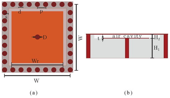
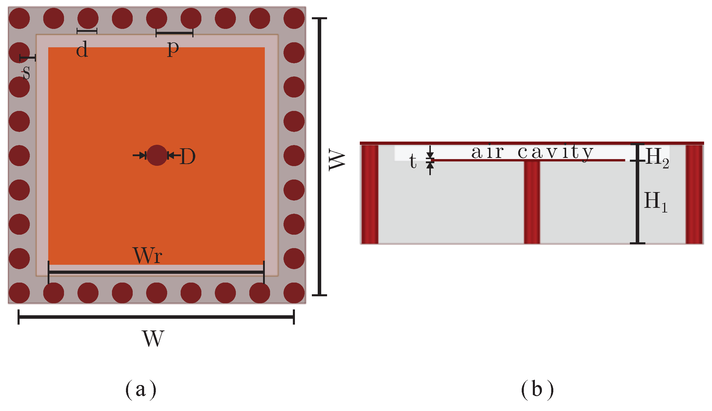
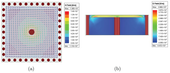
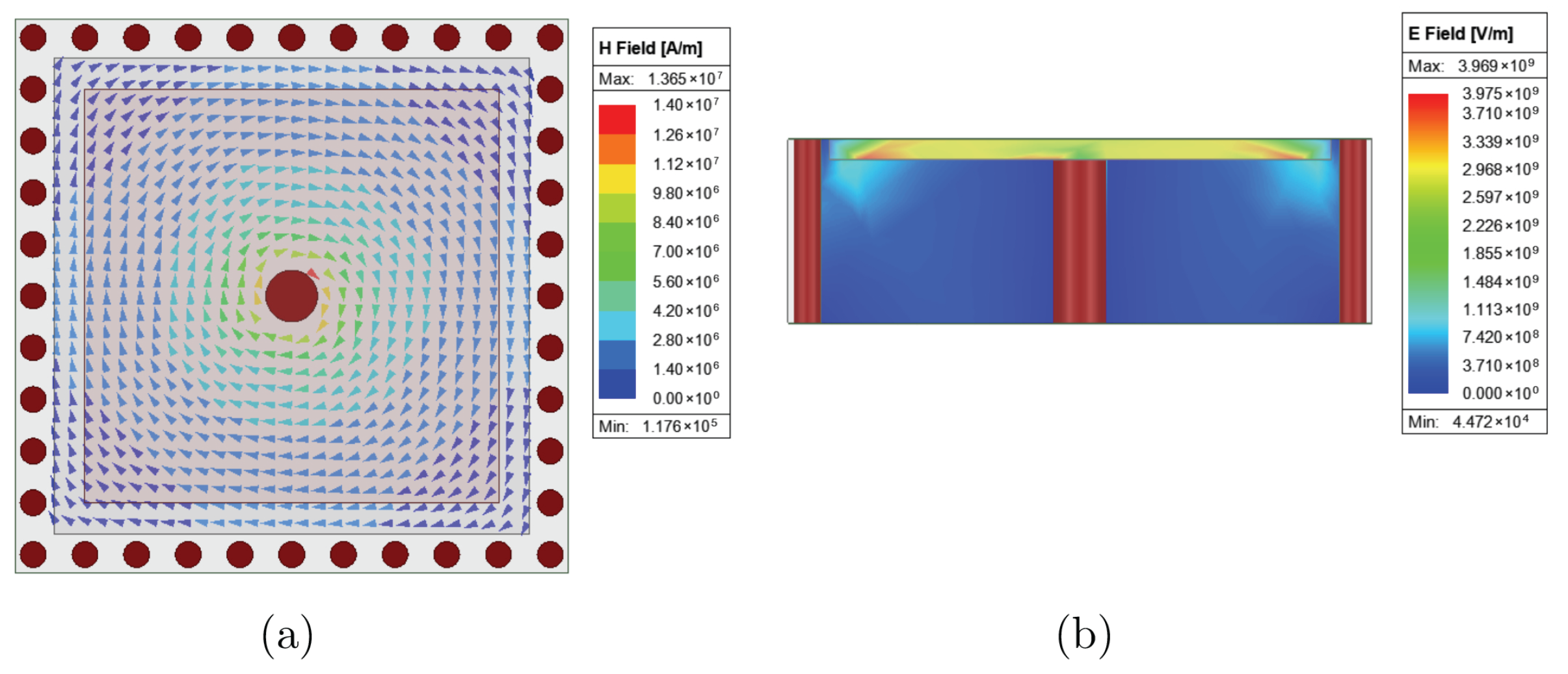
The proposed loaded SIW cavity is depicted in Figure 1. It is composed of a 3.378 mm TMM3 substrate (), a 0.0685 mm Isola prepreg (), and three metallic layers. TMM3 substrate has a dielectric constant of 3.55 and a loss tangent of 0.0021. The middle metallic patch is connected to the bottom layer through a metalized via of diameter (D) to form a highly capacitive loading embedded coaxial line cavity. On top of the patch, the prepreg is cut to remove the dielectric layer and create an air gap. The effective air gap above the patch is defined as the difference between the prepreg thickness used to form the air cavity and the copper thickness (t) of the metal patch. Consequently, the dielectric loss between the patch and the top layer, where the strongest electric fields exist, is eliminated. The electric and magnetic fields of the proposed cavity are demonstrated in Figure 2. The magnetic field around the post has a uniform ring-shaped distribution, and the electric field is strong and uniformly distributed between the patch and the cavity top. Thus, the resonator can be modeled as a short-circuited coaxial line and parallel plate capacitor [21].
Figure 1.
Proposed ELCSIW resonator (a) top view, and (b) cross-section view. The image is not drawn to scale, and dimensions are in mm (W = 10, = 7.5, s = 0.75, = 3.378, = 0.0685, D = 0.5, t = 0.0175, d = 0.5, p = 1).
Figure 2.
The ELCSIW resonator fields distribution (a) magnetic field, and (b) electric field.
The resonant frequency of the loaded coaxial cavity shown in Figure 1 can be determined by [21]
where c is the speed of light in free space, and is the characteristic admittance of the coaxial line formed by the loading patch, the post, and the outer square via walls. and denote the capacitance of the loading patch and the dielectric constant of the substrate, respectively. The capacitance has two components: a capacitance between the patch and the top layer () and the bottom layer (), and can be written as = + . When the perpendicular fields and fringe fields are included, and can be determined by [25]
where is the patch width, and g is the spacing between the capacitor walls. In this design, g corresponds to the thicknesses and .
The characteristic admittance of the coaxial line can be written as [26]
where D is the diameter of the coaxial inner conductor. is the effective width of the SIW cavity and can be written as [27]
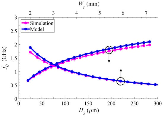
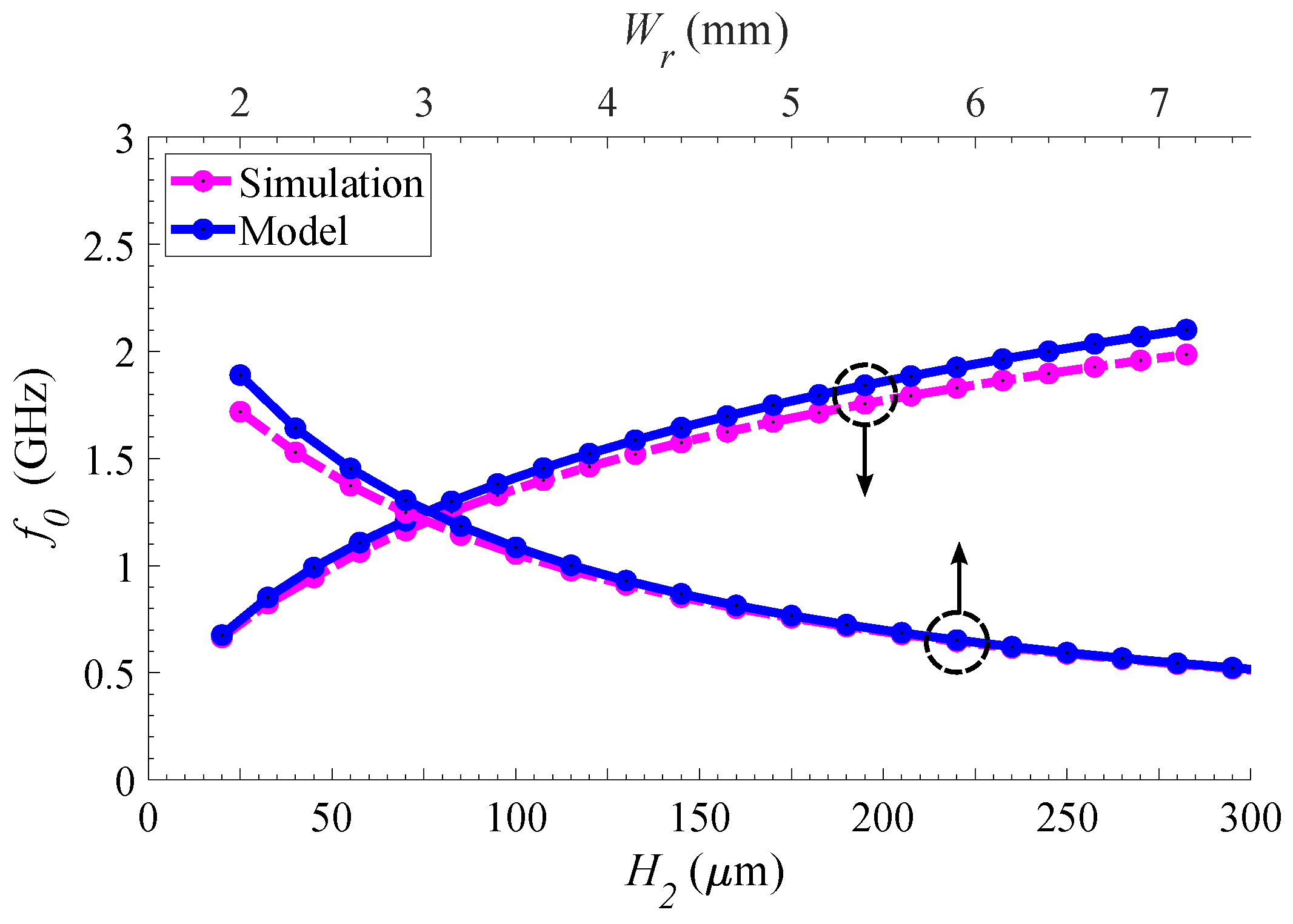
where W is the width of the SIW cavity, d is the diameter of the wall vias, and p is the spacing between vias. A comparison between the resonant frequency given by (1) and the simulation results using HFSS eigenmode of the loaded cavity is presented in Figure 3, showing good agreement.
Figure 3.
A comparison of the resonant frequency versus Isola prepreg thickness and patch width for the ELCSIW resonator shown in Figure 1. The arrows denote the associated horizontal axis (top or bottom). Simulation: eigenmode ANSYS HFSS 2022 R2 solver solution, Model: Loaded coaxial line model from (1).
The quality and miniaturization factors of the proposed ELCSIW cavity are primarily determined by , D, , and . The unloaded quality factor of the ELCSIW cavity resonator can be expressed as [28]
where , , and denote the dielectric, conductor, and radiation quality factors, respectively. determines the resonator’s internal losses and directly affects the filter’s overall insertion loss. characterizes the loss associated with the dielectric material, while accounts for ohmic losses associated with current flow in the cavity. These losses include losses along the central post, the surrounding via walls, and the three metal layers. Radiation loss is considered negligible because the structure is fully enclosed by SIW via walls and does not include open radiating edges [2]. Thus, the main loss contributions to the ELCISW resonator are dielectric and conductor losses. To quantify each loss, two eigenmode simulations at 1.1 GHz were performed for the resonator shown in Figure 1. The dielectric quality factor was extracted by enabling only dielectric loss and modeling all metallic layers as perfect electric conductors (PEC), which results in = 4780. This relatively high value is due to the fact that the electric field is concentrated in the dielectric-free air gap between the patch and the top layer, while only a small portion of the field exists in the dielectric region between the patch, the via walls, and the bottom layer. The conductor quality factor was obtained by assuming a lossless dielectric material with finite metal surface conductivity, resulting in = 570. In the proposed ELCSIW resonator, conductor loss is therefore the limiting factor. As the air gap thickness decreases, the capacitive loading increases, resulting in higher surface current density on the metallic layers. This effect increases ohmic losses and reduces the overall unloaded quality factor.
The miniaturization factor can be determined by
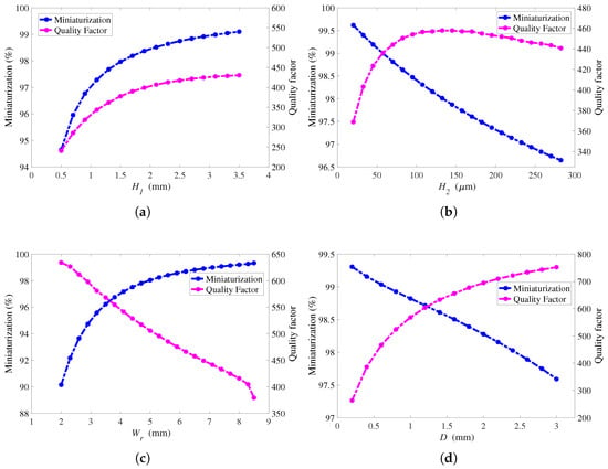
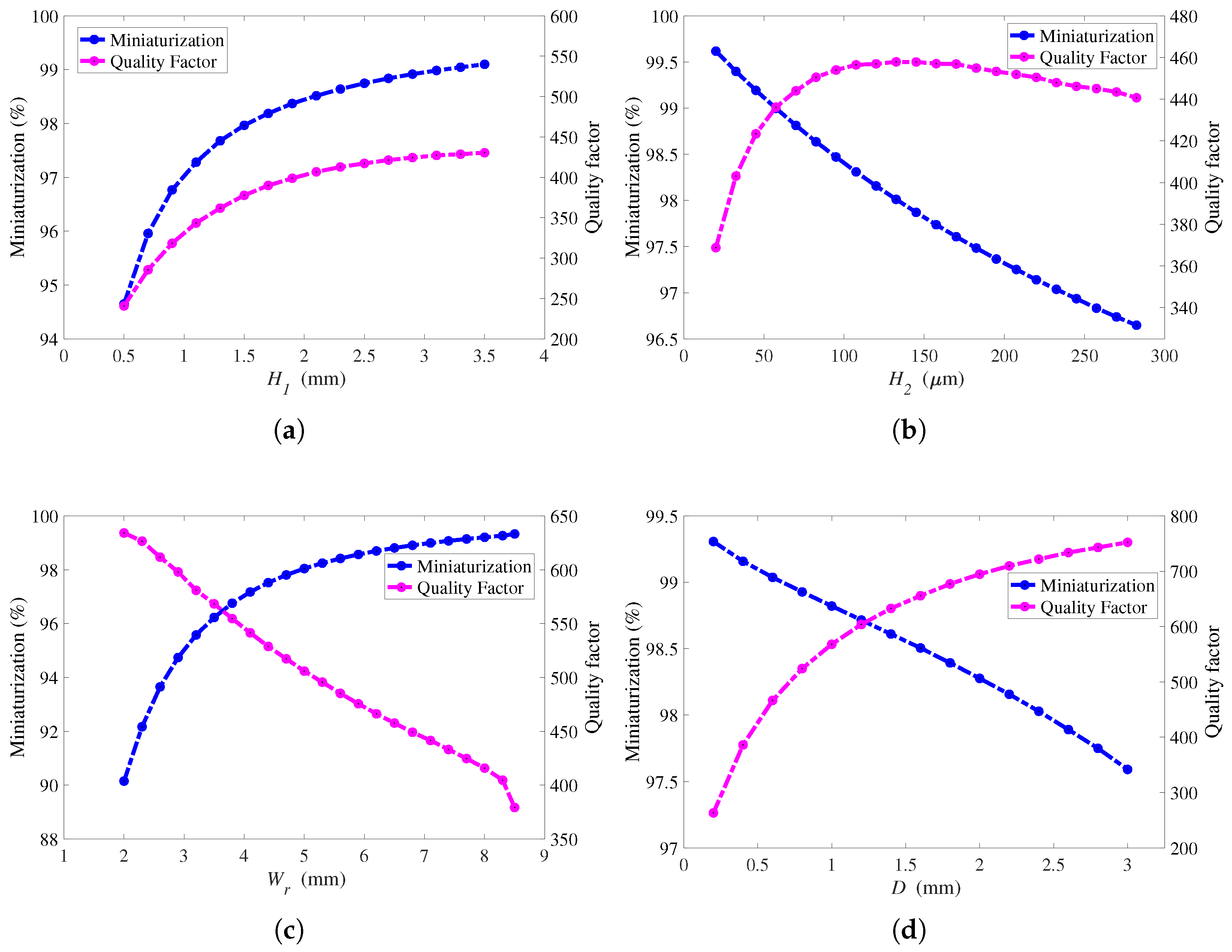
where is the physical area of the proposed ELCSIW cavity, and is the area of a conventional SIW cavity operating in the dominant mode at the same resonant frequency and implemented using the same dielectric substrate material. For instance, the reported miniaturization factor of 99% means that the ELCSIW resonator occupies only about 1% of the area of the equivalent conventional SIW cavity. To analyze the effects of the abovementioned parameters on the ELCSIW resonator, eigenmode simulations using the Ansys HFSS solver are performed for the cavity in Figure 1 and presented in Figure 4. Note that a finite copper conductivity (5.7 S/m) and a smooth metal surface (surface roughness set to 0 µm) were assumed, and the dielectric loss tangent of the substrate material was enabled in these simulations.
Figure 4.
Effects of key geometrical and substrate parameters on the miniaturization and quality factor of the ELCSIW resonator. (a) Dielectric substrate thickness , (b) Isola prepreg thickness , (c) patch width , and (d) post diameter D.
The miniaturization of the cavity size can be achieved through several approaches, including increased capacitive loading, reduced coaxial characteristic admittance, or increased substrate thickness . It is observed in Figure 4a that an increase in leads to a rise in inductance and a significant decrease in size. Similarly, a reduction in or an increase in results in increased loading capacitance, enabling higher degrees of miniaturization as presented in Figure 4b,c. However, it should be noted that increasing the capacitive loading reduces the overall quality factor due to increased parallel-plate losses between the middle patch and the top metallic layer. Thus, a trade-off between miniaturization and quality must be carefully examined and balanced to achieve optimal performance.
3. Filter Implementation
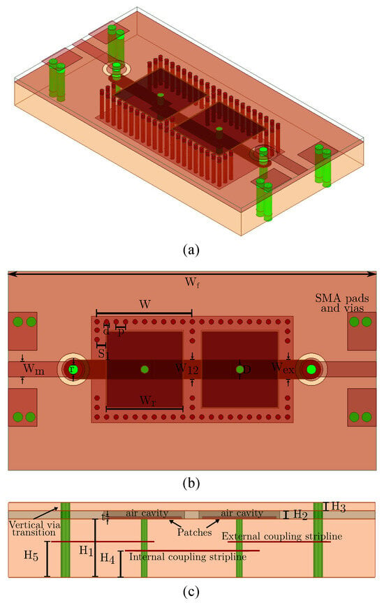
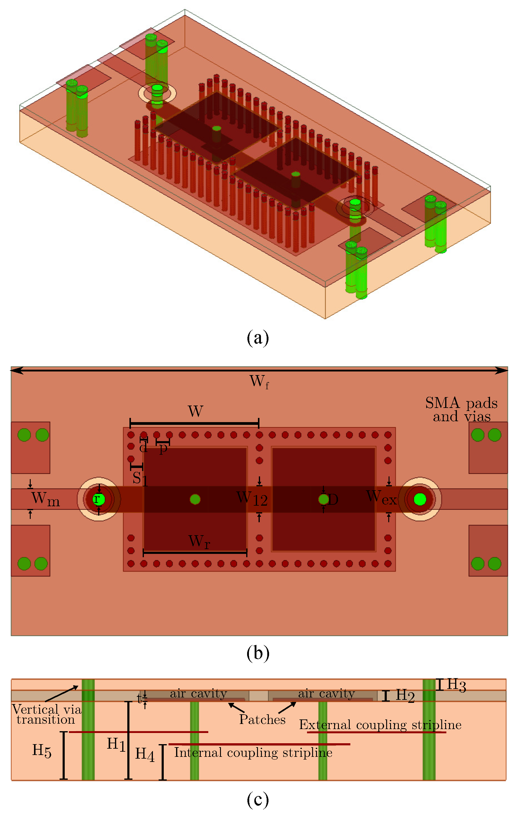
As depicted in Figure 5, the proposed ELCSIW resonator is employed to build a two-pole filter. The ELCSIW filter has a center frequency of 1.1 GHz, a fractional bandwidth of 6.3%, and an equi-ripple of 20 dB. To develop the two-pole filter, the generalized coupling matrix that meets the above requirements is generated and given as follows [29]:
Figure 5.
Proposed ELCSIW filter: (a) 3D view, (b) top view, and (c) cross-section view. The image is not drawn to scale.
Using the generalized coupling matrix, the inter-resonator coupling coefficients and the external quality factor () are then denormalized and determined by
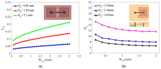
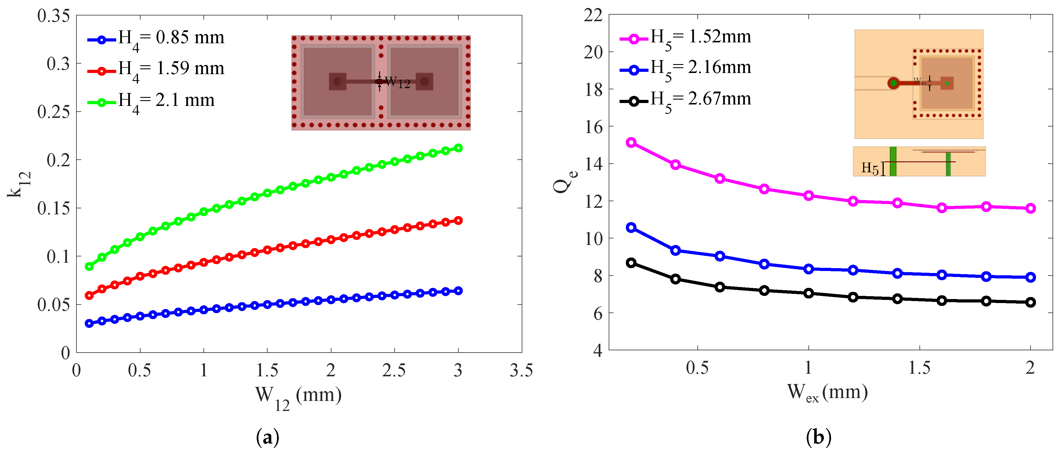
where is the coupling coefficient between two loaded SIW cavities, and FBW is the fractional bandwidth. The inter-resonator coupling coefficient () quantifies the strength of coupling between adjacent resonators, while the external quality factor () determines how strongly the feed line is coupled to the resonator. These two parameters determine the required filter bandwidth. The design procedure results in an inter-resonator coupling coefficient of 0.1045 and an external quality factor of 10.58. Due to the field distribution within the structure, where strong electric fields are concentrated in the air gap region, conventional inductive iris coupling provides insufficient coupling. Therefore, a direct magnetic coupling mechanism is employed using embedded striplines tap that connect the inner conductors of adjacent resonators. As illustrated in Figure 5, the inter-resonator coupling mechanism of the proposed filter is constructed by connecting neighboring resonators with an embedded stripline at the height of . This configuration creates a magnetic coupling that can be adjusted by the stripline’s height and width [20]. Inter-resonator coupling coefficient extraction is performed using weakly coupled resonators to obtain the height and width of the coupling stripline, and can be determined by [28]
where and are the coupled resonators’ split resonant-mode frequencies. Figure 6a shows that the stripline height and width are proportional to the inter-resonator coupling coefficient.
Figure 6.
(a) Inter-resonator coupling coefficient and (b) external quality factor as functions of stripline widths for different coupling stripline heights. The inset images are not drawn to scale.
For the external coupling configuration, the filter is fed by a 50 microstrip line and magnetically coupled through a vertical via that directly taps into the resonator post. The height and width of the striplines connecting to the posts determine the coupling intensity. The external quality factor is extracted using a single-loaded resonator, as determined by [28]
where denotes the angular resonant frequency and denotes the group delay at the angular resonant frequency. Figure 6 shows the extracted inter-resonator coupling coefficients and external quality factor for different stripline heights and widths. The observed trends indicate that the inter-resonator coupling coefficient () and the external quality factor () can be tuned by adjusting the geometric parameters , , and . The extracted coupling coefficients demonstrate the capability to synthesize both narrowband and wideband responses by properly adjusting the heights and widths of the embedded tapping striplines.
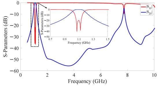
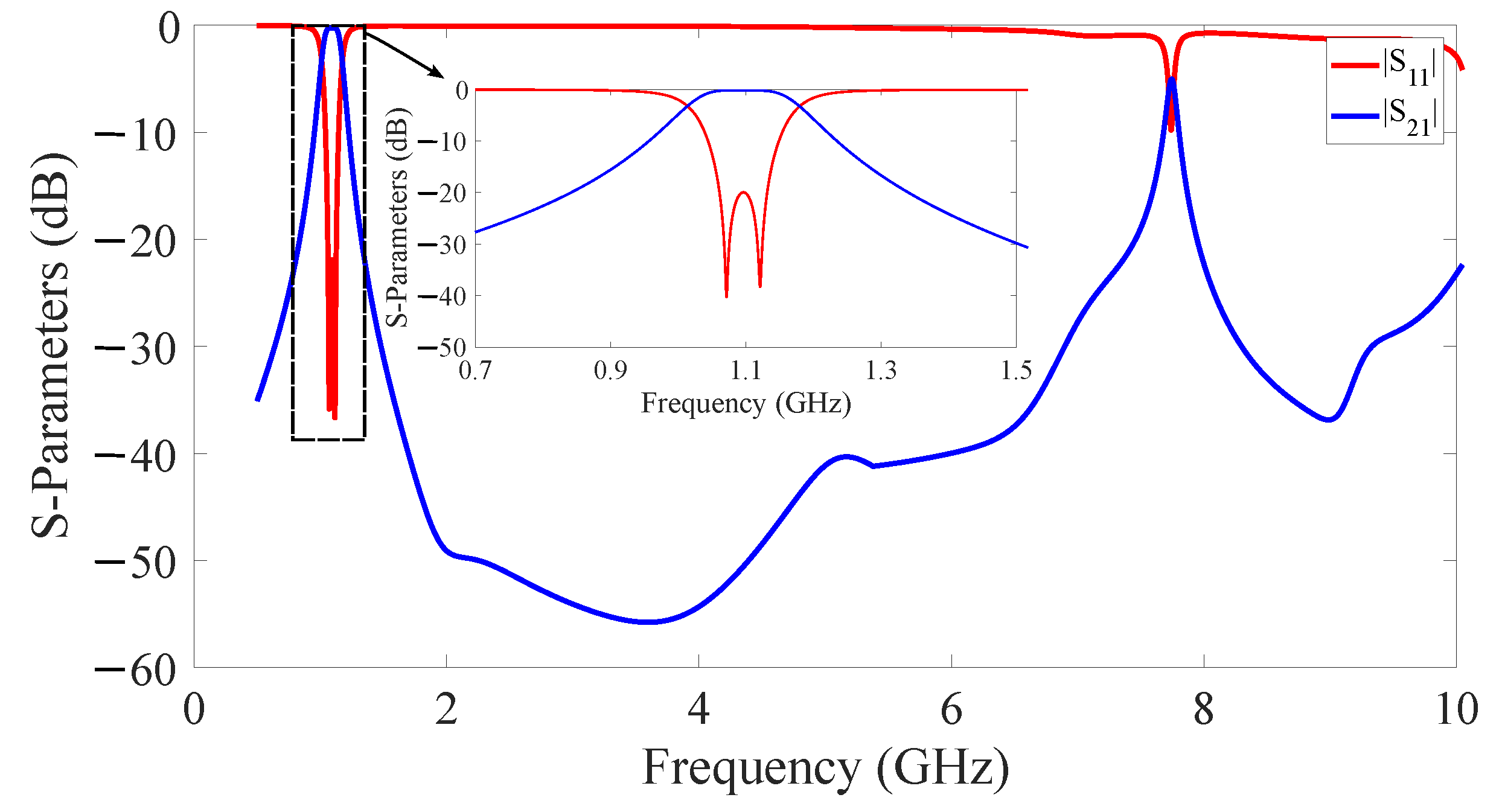
The filter’s dimensions and coupling coefficients are listed in Table 1. A full-wave HFSS solver is used to implement and simulate the proposed filter. In the simulations, copper conductivity is set to the value of 5.8 × S/m, and the copper clad surface roughness is modeled according to the manufacturer’s specification using the Groiss model. The S-parameters for the filter are presented in Figure 7, demonstrating a wide spurious-free upper band. This extended spurious-free response is attributed to the resonator’s modal properties. The proposed resonator operates in a loaded quasi-TEM mode. In this mode, the magnetic field circulates around the central post, while the electric field is strongly concentrated in the gap between the patch and the top metal layer. The first higher-order resonance corresponds to a cavity mode of the SIW structure. The central post and capacitive loading alter the field distribution in the SIW cavity, shifting the higher-order modes to higher frequencies [20]. This shift increases the separation between the fundamental quasi-TEM resonance and the first spurious response, allowing the filter to exhibit a wide spurious-free upper band. The full-wave simulation estimates a total insertion loss of 0.28 dB within the passband. This loss includes the coplanar waveguide (CPW) feeding lines and the microstrip-to-CPW transition losses. To extract the intrinsic filter performance, the transition losses were de-embedded by simulating back-to-back transitions. The additional loss caused by the two transitions was found to be 0.065 dB. Thus, the intrinsic simulated insertion loss of the filter is 0.215 dB. This loss is primarily attributed to the conductor loss, which results from the high surface current density concentrated along the capacitive patch, the top metal layer, and the inner coaxial conductor, as discussed above in Section 2. Further reduction in this loss can be achieved by employing higher-conductivity metallization for the cavity surfaces.
Table 1.
Dimensions of ELCSIW filter and its coupling coefficients. All dimensions in mm.
Figure 7.
Simulated S-parameters of the second-order ELCSIW filter showing the achieved wide spurious-free stopband. The inset figure shows a closer view of the filter passband.
4. Fabrication Process and Results
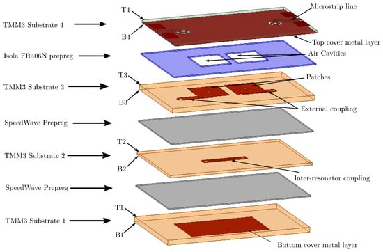
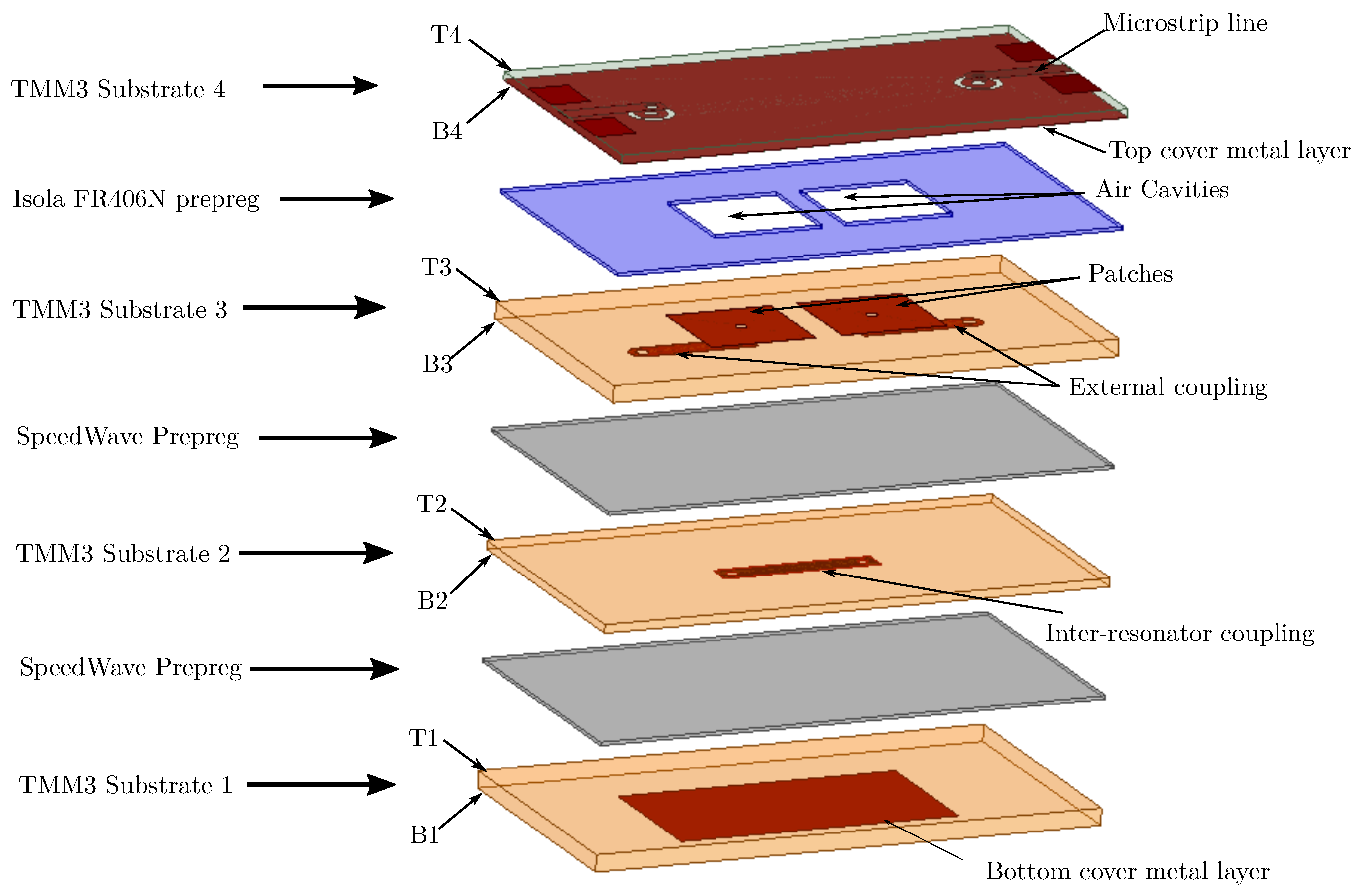
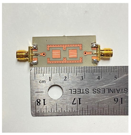
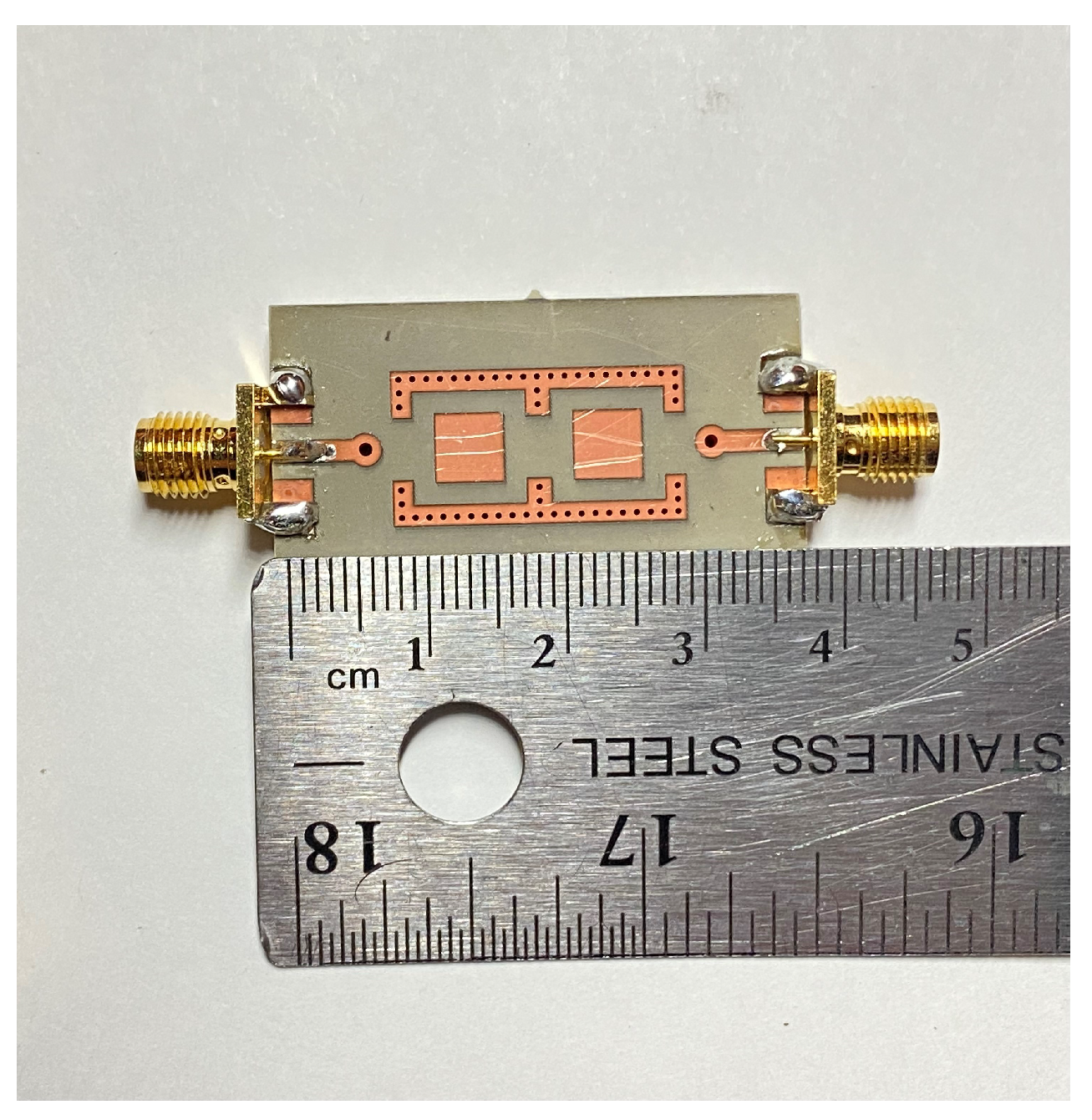
The proposed ELCSIW filter is fabricated using a multilayer printed circuit board (PCB) process. The stacked-up layers of the second-order ELCSIW filter are shown in Figure 8. The structure consists of a capacitively loaded SIW cavity with an embedded metallic patch connected to the cavity bottom through a plated-via post, forming a coaxial resonator. The high capacitive loading occurs between the patch and the top metallic layer. To eliminate dielectric loss in this high-field region, an embedded air cavity is introduced above the patch using a thin prepreg layer during lamination. Microstrip feed lines are designed on the top copper surface of Substrate 4 with a pair of copper pads on both sides that are short-circuited to the ground plane through plated vias. The microstrip lines are connected to the external tap striplines through plated vertical transition vias. The external coupling tap striplines are shorted to the posts on the bottom side of Substrate 3 (B3) at the height of , while the inter-resonator coupling tap stripline is placed on the bottom side of Substrate 2 (B2) at the height of . The metal patches are located on the top side of Substrate 3 (T3). The inter-resonator and external coupling taps are implemented on different substrate layers to control the filter coupling coefficients, which depend on the height and width of each tap line. Since dielectric loss directly impacts the unloaded quality factor , the primary substrate material must exhibit a low loss tangent and sufficient thickness to support high capacitive loading. Based on the design analysis in Figure 4, a cavity substrate thickness of 3 mm or more is preferred to achieve both high miniaturization and high quality factor. This thickness is achieved by stacking multiple dielectric layers bonded with prepreg sheets. Also, this multiple-layer stacking allows the coupling structures to be implemented at different vertical heights. Material selection is critical to ensure fabrication reliability, dimensional stability, and accurate control of resonant frequency variations caused by dimensional tolerances. The dielectric substrates need to have a high flexural strength to avoid bending during lamination. The coefficient of thermal expansion (CTE) of the dielectric substrate should match that of copper to minimize stress in plated vias, which may lead to current path discontinuities. Sufficient mechanical stiffness of the top substrate layer is required to prevent deformation into the cavity during lamination, which could reduce the air-gap height and alter the resonant frequency. Thus, thermoset microwave material (TMM3) is selected for the substrate layers because it offers a suitable combination of low dielectric loss, a relatively low CTE, and high mechanical stiffness. Standard 0.5-oz copper cladding (17.5 µm) is used, which is significantly larger than the copper skin depth at the operating frequency (2 µm at 1.1 GHz), ensuring negligible additional conductor loss. A key aspect of the fabrication is the formation of the air cavity using a low-flow prepreg material. Conventional prepregs exhibit significant resin flow during lamination. This resin can partially fill the air-gap region, affecting the loading capacitance and shifting the resonant frequency. Therefore, a low-flow prepreg (Isola FR406N) is used to maintain a uniform air-gap thickness. The filter is fabricated using multilayer PCB processes, including copper patterning, layer stacking, lamination, via drilling, and copper electroplating. A photograph of the assembled prototype is shown in Figure 9. Using this multilayer PCB process, the ELCSIW second-order filter prototype is fabricated with an embedded air-gap capacitive region. This approach enables the realization of an ultra-miniaturized loaded coaxial SIW resonator with significantly reduced dielectric loss, allowing for extreme miniaturization and a high unloaded quality factor.
Figure 8.
A 3D view of the stack-up layers of the second-order ELCSIW filter. Note that the vias of the ELCSIW cavity are not shown for clarity.
Figure 9.
Photograph of the fabricated second-order filter.
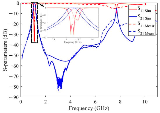
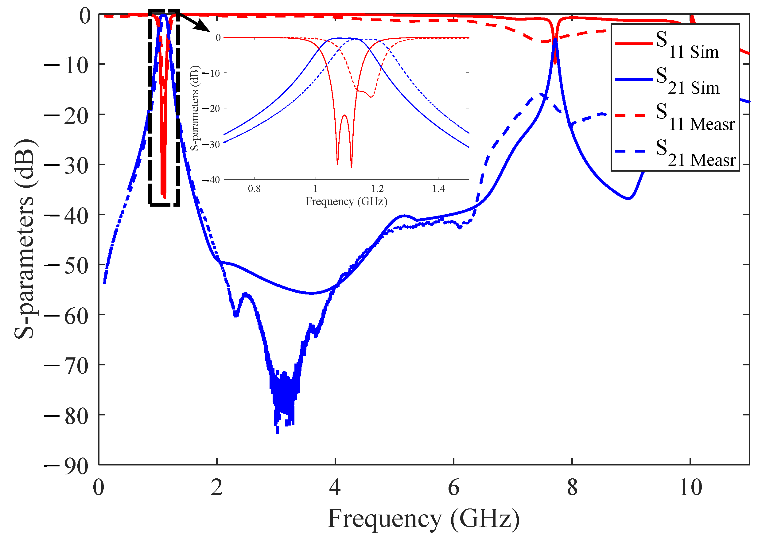
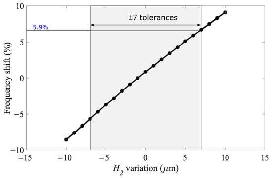
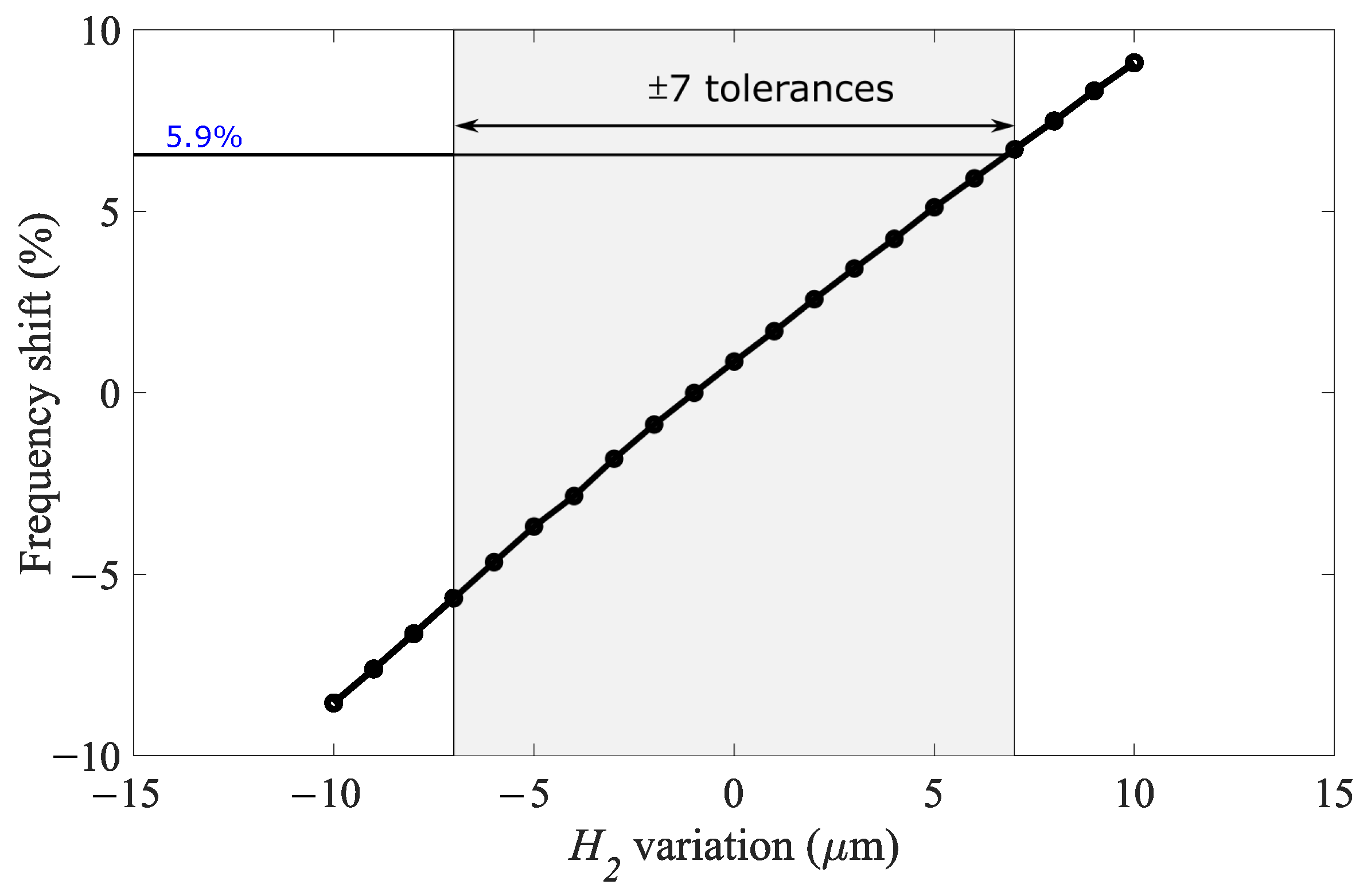
The filter’s simulated and measured results are compared in Figure 10. The measured in-band return loss is greater than 15 dB, and the upper filter stopband is free of spurious modes up to 7.5 GHz. The fractional bandwidth and insertion loss are measured to be 5.5% and 0.54 dB, respectively. The footprint of the filter excluding the feeding lines is 10.5 mm × 20.5 mm, which is equivalent to 0.07 × 0.14. A discrepancy between the simulated and measured results in terms of center frequency, return loss, and bandwidth is observed. This effect is attributed to the sensitivity of the proposed multilayer structure to vertical spacing tolerances. The Isola prepreg layer forming the highly capacitively loaded air gap region has a nominal thickness tolerance of ±7 µm [30]. Variations in this prepreg thickness can significantly affect the center frequency, contributing to the upward frequency shift as observed in the measured results. To validate this effect, a quantitative sensitivity analysis based on eigenmode simulations was conducted to evaluate the impact of Isola prepreg thickness () on the center frequency. The nominal value of is 68.5 µm with a manufacturing tolerance of ±7 µm. The results are presented in Figure 11 and show that ±7 µm thickness variations can cause up to a 5.9% shift in the resonant frequency. This analysis shows how critical thickness is to fabrication tolerance and explains the measured frequency shift. Variations in the prepreg and substrate thickness also affect the total stack-up height . The characteristic admittance of the coaxial line () depends on , as expressed in (3). Therefore, a reduction in results in a shift toward a higher resonant frequency, as expressed in (1). In addition, during lamination, the prepreg experiences resin flow and compression at high temperature and pressure, reducing the stack’s total thickness . Also, the filter’s inter-resonator and external stripline coupling depend on the vertical spacing between layers. The striplines heights directly determine the filter’s bandwidth and return loss through their control of the coupling strength, as shown in Figure 6. The external and inter-resonator coupling striplines are distributed across multiple TMM3 substrates and prepreg layers, each with manufacturing tolerances. The combination of these variations can lead to discrepancies in return loss and bandwidth, as observed in the measured results. These thickness variations impact the return loss, fractional bandwidth, and resonant frequency. Therefore, tighter control of the lamination process and careful consideration of layer-stacking tolerances would improve agreement between measured and simulated responses.
Figure 10.
The simulated and measured S-parameters of the second-order ELCSIW filter.
Figure 11.
The shift in the resonant frequency of the proposed ELCSIW resonator versus the variation in the Isola prepreg thickness (). The gray shaded region represents the thickness tolerance range of the Isola prepreg.
Higher-order filter responses can be realized by cascading additional ELCSIW resonators and employing the same coupling mechanisms with proper geometric tuning of the inter-resonator and external coupling structures. The ELCSIW structure is scalable to millimeter-wave frequencies. This can be realized through state-of-the-art manufacturing facilities capable of achieving the required dimensional tolerances and multilayer stack-up precision at these frequency scales.
Various SIW miniaturization techniques have been reported in the literature, with trade-offs between footprint reduction and resonator performance presented in Table 2. The compact SIW cavities in [8,9] employ the sub-mode technique to achieve substantial footprint reduction. In [8], the cavity is further combined with ridge loading and folding to achieve a miniaturization factor of approximately 96.4%, while in [9], a thirty-second-mode SIW cavity representing only 1/32 of the original cavity resonates at the fundamental mode. Despite its extreme compactness, this technique introduces open cavity boundaries, with a strong electric field near the edges and increased radiation and conductor losses, which limit the unloaded quality factor to below 100. Another miniaturization approach utilizes a composite right/left-handed (CRLH) structure in a SIW cavity [18]. In this design, interdigital capacitive slots increase the effective loading capacitance and reduce the resonant frequency, achieving a miniaturization factor of 89.7% for a second-order filter with 3.4% fractional bandwidth. However, the high electric field in the interdigital regions increases conductor and radiation losses, resulting in a low of 96. In [15], a multilayer quadri-folded SIW cavity coupled through a C-type slot is proposed to achieve 89% miniaturization. However, the folding structure introduces high currents near the slot. This effect increases conductor and dielectric losses, limiting the quality factor to about 120. In [10], a compact filter based on a half-mode substrate integrated coaxial resonator (HMSICR) is proposed. The structure is obtained by bisecting a substrate-integrated coaxial cavity and vertically stacking the resonators, resulting in a miniaturization of approximately 97.2%. Despite the high level of miniaturization, the half-mode SICR configuration introduces an open boundary that increases field leakage and conductor loss. In addition, the capacitive loading across the dielectric-filled gap in the coaxial structure further increases dielectric loss. As a result, the unloaded quality factor is limited to approximately 217. Similarly, dielectric-loaded coaxial SIW cavities reported in [20,21,24] achieve miniaturization by a capacitive loading between a metal patch and the top cavity wall across a thin dielectric layer. In [20], this approach results in a miniaturization factor of approximately 96.8% and an unloaded quality factor of 165, while the design in [21] achieves of 325. In [24], the miniaturization is further increased to 98.81%. This is accomplished by introducing a coupled split-ring CPW structure, which increases the effective loading capacitance and reduces the cavity size at the operating frequency. However, the electric field concentration within the dielectric region results in an unloaded quality factor of about 177. In contrast to reported techniques, the proposed ELCSIW resonator achieves high miniaturization by a strong capacitive loading within a fully enclosed multilayer cavity. The capacitive loading is formed across an embedded air cavity where the maximum electric field is located. By removing dielectric material from the dominant capacitive region, the ELCSIW structure eliminates the dielectric loss in this region. Thus, the proposed resonator achieves 99% miniaturization while maintaining an unloaded quality factor of about 500. This exceeds the performance reported in the aforementioned works. This result highlights the capability of the ELCSIW configuration to achieve both extreme compactness and high intrinsic resonator performance.
Table 2.
Comparison between the related works in the literature and the proposed ELCSIW filter.
5. Conclusions
This paper proposes an ultra-miniaturized and high-Q embedded loaded coaxial SIW resonator. The ELCSIW resonator surpasses reported compact SIW resonators, achieving 99% miniaturization and a Q-factor of 500. An ultra-miniaturized and low-loss two-pole BPF is designed and fabricated to demonstrate the benefits of the proposed structure. The filter shows a low insertion loss of 0.54 dB and a wide spurious-free upper band up to 7 times the resonant frequency. The simulation and measurement results are in good agreement. The presented ultra-miniaturized filter is attractive for compact, advanced wireless systems due to its significantly reduced footprint, planar configuration, and low insertion loss.
Author Contributions
Conceptualization, N.R.A.; Methodology, N.R.A. and H.H.S.; Software, N.R.A.; Validation, N.R.A., G.A. and H.H.S.; Formal analysis, N.R.A. and H.H.S.; Investigation, N.R.A. and G.A.; Resources, H.H.S.; Writing—original draft, N.R.A., G.A. and H.H.S.; Writing—review & editing, N.R.A., G.A. and H.H.S.; Visualization, N.R.A.; Supervision, H.H.S.; Project administration, N.R.A.; Funding acquisition, N.R.A. All authors have read and agreed to the published version of the manuscript.
Funding
This research was funded by the Deanship of Scientific Research (DSR) at King Abdulaziz University, Jeddah, Saudi Arabia: (IPP:1083-829-2025).
Data Availability Statement
The original contributions presented in this study are included in the article. Further inquiries can be directed to the corresponding author.
Acknowledgments
The authors would like to acknowledge, with thanks, the Deanship of Scientific Research at King Abdulaziz University for its technical and financial support.
Conflicts of Interest
Author Gokhan Ariturk was employed by the company Texas Instruments. The remaining authors declare that the research was conducted in the absence of any commercial or financial relationships that could be construed as a potential conflict of interest.
References
- Deslandes, D.; Wu, K. Single-substrate integration technique of planar circuits and waveguide filters. IEEE Trans. Microw. Theory Tech. 2003, 51, 593–596. [Google Scholar] [CrossRef] [Scilit]
- Wu, K.; Bozzi, M.; Fonseca, N.J.G. Substrate integrated transmission lines: Review and applications. IEEE J. Microwaves 2021, 1, 345–363. [Google Scholar] [CrossRef] [Scilit]
- Chen, X.P.; Wu, K. Substrate Integrated Waveguide Filter: Basic Design Rules and Fundamental Structure Features. IEEE Microw. Mag. 2014, 15, 108–116. [Google Scholar] [CrossRef] [Scilit]
- Wu, L.; Izquierdo, B.S.; Young, P.R. Half-mode substrate integrated waveguide (HMSIW) bandpass filter. IEEE Antennas Propag. Soc.-Ap-S Int. Symp. (Digest) 2007, 17, 265–267. [Google Scholar] [CrossRef] [Scilit]
- Moscato, S.; Tomassoni, C.; Bozzi, M.; Perregrini, L. Quarter-Mode Cavity Filters in Substrate Integrated Waveguide Technology. IEEE Trans. Microw. Theory Tech. 2016, 64, 2538–2547. [Google Scholar] [CrossRef] [Scilit]
- Liu, D.; Dong, Y. Compact Low-Loss Half-Mode Substrate Integrated Waveguide Filter With Controllable Transmission Zeros. IEEE Trans. Circuits Syst. II Express Briefs 2022, 69, 4248–4252. [Google Scholar] [CrossRef] [Scilit]
- Almuqati, N.R.; Ariturk, G.; Sigmarsson, H.H. Empirical Quality Factor Prediction of Quarter-Mode Substrate Integrated Waveguide Resonators. IEEE J. Microwaves 2021, 1, 777–786. [Google Scholar] [CrossRef] [Scilit]
- Jones, T.R.; Daneshmand, M. Miniaturized Folded Ridged Half-Mode and Quarter-Mode Substrate Integrated Waveguides for Filter Design. IEEE Trans. Microw. Theory Tech. 2019, 67, 3414–3426. [Google Scholar] [CrossRef] [Scilit]
- Yang, Y.N.; Li, G.H.; Sun, L.; Yang, W.; Yang, X.X. Design of compact bandpass filters using sixteenth mode and thirty-second mode SIW cavities. Prog. Electromagn. Res. Lett. 2018, 75, 61–66. [Google Scholar] [CrossRef] [Scilit]
- Ho, M.H.; Hsu, C.I.G.; Tang, K.H.; Hong, W. Miniaturized Band Pass Filter Design Using Half Mode Substrate Integrated Coaxial Resonators. Micromachines 2022, 13, 389. [Google Scholar] [CrossRef] [Scilit] [PubMed]
- Li, P.; Chu, H.; Chen, R.S. Design of compact bandpass filters using quarter-mode and eighth-mode SIW cavities. IEEE Trans. Components Packag. Manuf. Technol. 2017, 7, 956–963. [Google Scholar] [CrossRef] [Scilit]
- Qian, L.; Zhu, L.; Xu, J.; Chen, W.; Yu, Z.; Zhou, J.; Hong, W. Manufacture-Friendly Millimeter-Wave Filter Based on Double-Folded SIW Resonators. IEEE Microw. Wirel. Technol. Lett. 2025, 35, 1296–1299. [Google Scholar] [CrossRef] [Scilit]
- Liu, Q.; Zhang, D.W.; Gong, K.; Qian, H.; Qu, W.Z.; An, N. Single- and Dual-Band Bandpass Filters Based on Multiple-Mode Folded Substrate-Integrated Waveguide Cavities. IEEE Trans. Microw. Theory Tech. 2023, 71, 5335–5345. [Google Scholar] [CrossRef] [Scilit]
- Chien, H.Y.; Shen, T.M.; Huang, T.Y.; Wang, W.H.; Wu, R.B. Miniaturized bandpass filters with double-folded substrate integrated waveguide resonators in LTCC. IEEE Trans. Microw. Theory Tech. 2009, 57, 1774–1782. [Google Scholar] [CrossRef] [Scilit]
- Zhang, C.A.; Cheng, Y.J.; Fan, Y. Quadri-folded Substrate Integrated Waveguide Cavity and its Miniaturized Bandpass Filter Applications. Prog. Electromagn. Res. 2011, 23, 1–14. [Google Scholar] [CrossRef] [Scilit]
- Dong, Y.; Itoh, T. Substrate integrated waveguide negative-order resonances and their applications. IET Microwaves Antennas Propag. 2010, 4, 1081–1091. [Google Scholar] [CrossRef] [Scilit]
- Yang, T.; Chi, P.L.; Xu, R.; Lin, W. Folded Substrate Integrated Waveguide Based Composite Right/Left-Handed Transmission Line and Its Application to Partial H -Plane Filters. IEEE Trans. Microw. Theory Tech. 2013, 61, 789–799. [Google Scholar] [CrossRef] [Scilit]
- Hu, S.; Gao, Y.; Zhang, X.; Zhou, B. Design of a Compact 5.7–5.9 GHz Filter Based on CRLH Resonator Units. Prog. Electromagn. Res. Lett. 2020, 89, 141–149. [Google Scholar] [CrossRef] [Scilit]
- Joshi, H.; Sigmarsson, H.H.; Peroulis, D.; Chappell, W.J. Highly loaded evanescent cavities for widely tunable high-Q filters. In Proceedings of the 2007 IEEE/MTT-S International Microwave Symposium, Honolulu, HI, USA, 3–8 June 2007; pp. 2133–2136. [Google Scholar] [CrossRef] [Scilit]
- Sirci, S.; Martínez, J.D.; Boria, V.E. A novel magnetic coupling for miniaturized bandpass filters in embedded coaxial SIW. Appl. Sci. 2019, 9, 394. [Google Scholar] [CrossRef] [Scilit]
- Ho, M.H.; Li, J.C.; Chen, Y.C. Miniaturized SIW cavity resonator and its application in filter design. IEEE Microw. Wirel. Components Lett. 2018, 28, 651–653. [Google Scholar] [CrossRef] [Scilit]
- Joshi, H.; Sigmarsson, H.H.; Moon, S.; Peroulis, D.; Chappell, W.J. High Q narrow-band tunable filters with controllable bandwidth. In Proceedings of the 2009 IEEE MTT-S International Microwave Symposium Digest, Boston, MA, USA, 7–12 June 2009; pp. 629–632. [Google Scholar] [CrossRef] [Scilit]
- Moon, S.; Sigmarsson, H.H.; Joshi, H.; Chappell, W.J. Substrate Integrated Evanescent-Mode Cavity Filter With a 3.5 to 1 Tuning Ratio. IEEE Microw. Wirel. Components Lett. 2010, 20, 450–452. [Google Scholar] [CrossRef] [Scilit]
- Ho, M.H.; Hung, C.M.; Hsu, C.I.G. Filter Design Using Ultra-Miniaturised Substrate-Integrated Coaxial Cavity. IET Microwaves Antennas Propag. 2025, 19, e70017. [Google Scholar] [CrossRef] [Scilit]
- Palmer, H.B. The capacitance of a parallel-plate capacitor by the Schwartz-Christoffel transformation. Trans. Am. Inst. Electr. Eng. 2009, 56, 363–366. [Google Scholar] [CrossRef] [Scilit]
- Martinez, J.D.; Sirci, S.; Taroncher, M.; Boria, V.E. Compact CPW-fed combline filter in substrate integrated waveguide technology. IEEE Microw. Wirel. Components Lett. 2012, 22, 7–9. [Google Scholar] [CrossRef] [Scilit]
- Lai, Q.; Fumeaux, C.; Hong, W.; Vahldieck, R. Characterization of the propagation properties of the half-mode substrate integrated waveguide. IEEE Trans. Microw. Theory Tech. 2009, 57, 1996–2004. [Google Scholar] [CrossRef] [Scilit]
- Hong, J.S. Microstrip Filters for RF/Microwave Applications; John Wiley & Sons, Ltd.: Hoboken, NJ, USA, 2001; Chapter 3; pp. 29–76. [Google Scholar]
- Cameron, R.J.; Kudsia, C.M.; Mansour, R.R. Microwave Filters for Communication Systems: Fundamentals, Design and Applications; John Wiley & Sons, Ltd.: Hoboken, NJ, USA, 2018; Chapter 8; pp. 247–294. [Google Scholar]
- Corporation, R. SpeedWave™ 300P Prepreg DataSheet. 2023. Available online: https://www.rogerscorp.com/advanced-electronics-solutions/prepregs-and-bondplys/speedwave-300p-prepreg (accessed on 1 January 2023).
- Cohn, S.B. Dissipation Loss in Multiple-Coupled-Resonator Filters. Proc. IRE 1959, 47, 1342–1348. [Google Scholar] [CrossRef] [Scilit]

Disclaimer/Publisher’s Note: The statements, opinions and data contained in all publications are solely those of the individual author(s) and contributor(s) and not of MDPI and/or the editor(s). MDPI and/or the editor(s) disclaim responsibility for any injury to people or property resulting from any ideas, methods, instructions or products referred to in the content. |
© 2026 by the authors. Licensee MDPI, Basel, Switzerland. This article is an open access article distributed under the terms and conditions of the Creative Commons Attribution (CC BY) license.