


Abstract
The three-phase line-voltage cascaded Boost high power factor rectifier topology has been extensively studied for front-end rectification in high-power charging equipment. However, obvious current distortion occurs near the input voltage zero-crossing point under high-power conditions, which introduces severe harmonics and degrades system stability. Conventional studies often attribute zero-crossing distortion to spike distortion and discontinuous inductor conduction, yet these explanations cannot fully account for the waveform distortion observed in practical engineering scenarios. Based on the one-cycle controlled three-phase Boost PFC converter, this paper establishes a dynamic model to analyze the evolution of distortion under power-frequency grid and various load conditions. The study reveals the key source of current zero-crossing distortion: the fundamental phase shift of input current induced by inductor inertia and digital control delay. Furthermore, a reference current phase-lead scheme is adopted to suppress current zero-crossing distortion. Simulation and experimental results demonstrate that the proposed model can accurately capture current distortion characteristics. This phase compensation strategy can effectively improve the input current waveform, reduce harmonic content and enhance system stability near the rated operating condition, providing theoretical basis and technical support for the optimal design of PFC systems in high-power DC charging piles.
1. Introduction
Unidirectional electric vehicle (EV) charging piles dominate practical applications owing to their lower implementation cost compared with bidirectional chargers [1,2]. Bidirectional chargers support both charging and discharging, which complicates topology, control and protection schemes. Additional functions including anti-reverse power feed, anti-islanding and overcurrent protection are mandatory, raising both hardware expense and software complexity.
By contrast, unidirectional chargers only transfer power from the grid to batteries. The front-end diode rectifier blocks reverse power flow inherently at the topological level. It prevents battery backfeeding under faults such as charging-port short circuits and improves operational reliability [3]. Since no active power is fed back to the grid, islanding risk is eliminated. The strict anti-islanding compliance for distributed energy resources is unnecessary, which simplifies safety logic and reduces overall system complexity and engineering cost.
However, conventional unidirectional charging piles employ a diode rectifier front-end with a large DC-side filter capacitor. Diodes conduct only when the instantaneous grid voltage exceeds the capacitor voltage, which narrows the conduction angle in each fundamental cycle. This yields discontinuous pulse-shaped grid current, deviating from the sinusoidal waveform synchronized with grid voltage. The resulting severe current distortion and harmonic pollution deteriorate grid power quality and violate grid-code requirements for high-power power-electronic equipment, forming a major bottleneck for power rating upgrading of charging piles [4].
With advances in power factor correction (PFC), AC/DC converters can operate at near-unity power factor to reshape grid-side current and suppress input distortion, matching the trend of power-electronic systems toward high efficiency, low harmonics and low electromagnetic interference. The front-end PFC rectifier dominates the overall efficiency, grid-tied power factor and grid compatibility of high-power charging piles, rendering it a critical component for charger design and optimization [5].
To fulfill the demand for high-power charging, the topology construction of current charging pile power systems mainly relies on modular rectifier units. Three-phase two-level or three-phase Vienna rectifiers are widely adopted as the core topological units, combined with modular architectures such as line-voltage cascading or interleaved parallel connection to achieve power expansion [6,7]. However, in conventional two-level and interleaved parallel architectures, the intensive deployment of a large number of active switching devices inevitably increases system hardware redundancy, significantly raising the complexity and optimization difficulty of control strategy design. In contrast, the line-voltage cascaded topology proposed in Ref. [8] can effectively reduce the number of power switching devices and fast recovery diodes under the same power transmission level. It not only lowers the voltage stress of each power device but also achieves dual optimization of control complexity and hardware cost, providing a new technical approach and solution for the design of high-performance PFC conversion units in high-power charging piles.
Although the three-phase line-voltage cascaded Boost high power factor rectifier topology offers many advantages, its inherent residual current distortion during operation is particularly prominent under high-power and wide-load conditions. Such distortions are mainly concentrated near the current zero-crossing points, forming typical zero-crossing distortion phenomena. This phenomenon can lead to excessive harmonic content and reduced system stability. In severe cases, it may even cause false protection actions, directly threatening the safe and stable operation of charging equipment and the power grid. It has become one of the key factors restricting the performance improvement of high-power charging piles.
Conventional research predominantly attributes zero-crossing distortion to spike distortion and the intermittent conduction of inductance discontinuous conduction [9], which makes it difficult to fully explain waveform distortion phenomena in practical engineering applications and also prevents the targeted proposal of effective suppression methods. Under conventional power frequency steady-state conditions, such distortions have small amplitudes and limited impact on overall system performance, so a systematic mechanism analysis and theoretical explanation framework has yet to be formed. However, in high-performance operation scenarios of large-power charging piles, the coupling effects of complex operating conditions such as strong interference, wide input voltage range and large-range dynamic load switching significantly exacerbate zero-crossing distortion. Therefore, there is an urgent need to conduct research on the mechanism revelation and suppression technologies for this type of distortion [10].
Refs. [11,12,13,14,15,16] conducted in-depth research on the PFC rectifier topology for unidirectional energy flow at the mechanism level, pointing out that the distortion of the grid voltage zero-crossing point is induced by the coupling of multiple factors, which can mainly be summarized into three aspects. Firstly, the instantaneous amplitude at grid voltage zero-crossing points nears zero, leading to an inadequate effective driving voltage for the inductance and significantly constraining the dynamic current tracking capability, consequently resulting in a lag in reference current tracking and directly inducing current distortion [11]. Secondly, the load fluctuation range of charging piles is wide. The equivalent gain of current loops varies dynamically with the load, leading to a decrease in system phase margin and deterioration of damping characteristics. This further affects the dynamic response in the zero-crossing region and exacerbates current distortion [12]. Thirdly, the inherent phase lead characteristics of the system’s input voltage and current, when combined with the aforementioned issues [13], cause the current to cut off prematurely before the voltage zero-crossing point. Additionally, influenced by the unidirectional clamping effect of the rectifier bridge [14], there is a significant current overshoot and oscillation after the zero-crossing point. The coupled effects of multiple mechanisms collectively exacerbate the current distortion problem in the zero-crossing region. However, the aforementioned studies predominantly concentrate on conventional PFC rectification topology and fail to provide an in-depth analysis and systematic exposition of the current distortion characteristics pertinent to the three-phase PFC converter discussed in this paper. Meanwhile, research on the multi-factor coupling mechanism of zero-crossing distortion in three-phase PFC converters under high-power and wide-load conditions remains insufficient. Existing theoretical models exhibit obvious limitations, failing to fully reveal the essence of distortion and thus unable to provide a solid theoretical basis for the design of distortion suppression schemes. Therefore, it is necessary to further deepen the modeling and analysis of the internal distortion mechanism. Notably, current zero-crossing distortion—especially the zero-crossing distortion dominated by odd harmonics with insignificant even harmonics—is a typical and widespread issue in high-power charging applications, and becomes particularly severe under wide-load and high-frequency ripple input conditions. As the power rating of charging piles increases and grid-side harmonic suppression requirements become stricter, the impacts of supply frequency fluctuations and ripple components on the converter are intensified. The rate of change of the input voltage at the zero crossing increases significantly, greatly increasing the difficulty of real-time current tracking [15]. The neural-network-based DC-bus voltage calibration method presented in [16] offers strong disturbance rejection capability, such adaptive neural schemes demand heavy online computation. Meanwhile, under high-frequency operation, magnetic saturation, high-frequency losses and stray leakage inductance effects of the power inductor further degrade the dynamic response performance of the current loop. Ultimately, the zero-crossing distortion problem is significantly amplified, becoming a core technical bottleneck that urgently needs to be addressed in high-power PFC converters. For modular cascaded and parallel AC-DC converters, parameter mismatch and unbalanced load distribution may induce inter-module circulating currents, which increase device current stress and power loss. Ref. [17] presents a scalable filter topology based on coupled inductors for multi-module parallel converters, which suppresses cross-module circulating current by introducing secondary series loops. Nevertheless, extra magnetic components and contactors are required, which increases volume and cost. Sun investigated the zero-crossing distortion problem of single-phase average-current-controlled Boost PFC converters in [18]. Different from the conventional understanding attributing distortion to cusp distortion or DCM effect, his work pointed out two essential origins: the inherent current leading-phase effect and insufficient damping of the current loop. On this basis, a reference current phase-delay compensation scheme was proposed to mitigate zero-crossing distortion for single-phase applications. Nevertheless, the above analysis and compensation method are oriented to single-phase diode-bridge PFC topology, which cannot be directly applied to the line-voltage cascaded three-phase Boost PFC with one-cycle control studied in this paper.
Nevertheless, existing investigations mostly focus on conventional PFC topologies. The zero-crossing distortion mechanism unique to the line-voltage cascaded Boost rectifier remains insufficiently understood, and dedicated suppression methods are lacking.
This paper investigates the input current phase lag and resultant severe zero-crossing distortion across wide load ranges for the line-voltage cascaded Boost PFC rectifier presented in [8]. Taking the single-cycle controlled three-phase line-voltage cascaded PFC converter as the research subject, this work develops its dynamic model and reveals the distortion mechanism arising jointly from current phase lag and underdamped current loops. On this basis, an improved single-cycle control scheme with reference-current phase-lead compensation is proposed. The scheme compensates the phase lag and mitigates zero-crossing distortion over wide load conditions, offering a feasible approach for harmonic reduction and dynamic performance optimization of high-power grid-tied PFC converters.
The rest of this paper is organized as follows. Section 2 establishes the steady-state and small-signal models of the rectifier based on single-cycle control principles and introduces the topology and inherent characteristics of the line-voltage cascaded rectifier. Section 3 analyzes the inherent fundamental phase-shift and the generation mechanism of input-current zero-crossing distortion using the developed models. Section 4 proposes the reference-current phase-lead compensation control strategy to mitigate phase shift and current distortion. Section 5 verifies the performance of the proposed control scheme by simulation results. Finally, Section 6 concludes this paper.
2. Topology and Inherent Characteristics of Line-Voltage Cascaded Boost Rectifier
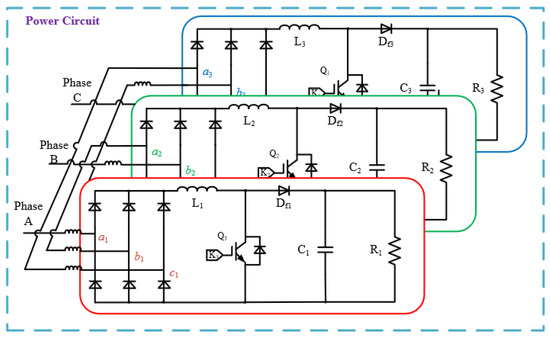
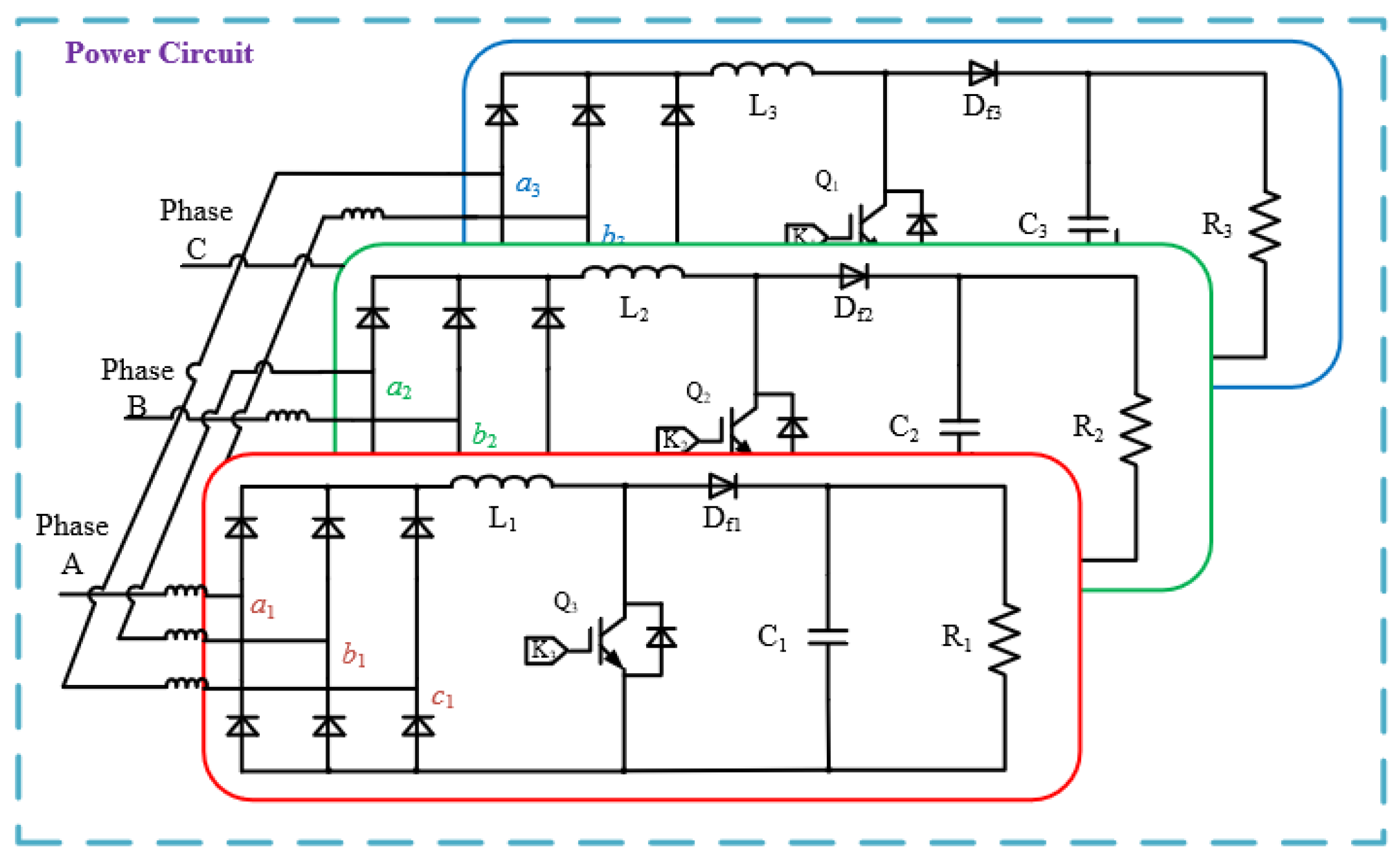
The topology and control strategy of the line-voltage-cascaded three-phase high power factor rectifier investigated in this paper are illustrated in Figure 1 [8]. Although numerous studies have expounded on the fundamental operational mechanism of the three-phase line-voltage-cascaded Boost converter utilizing a single-cycle approach, a concise overview of its topology and core operational principles remains essential to ensure the coherence and comprehensiveness of the theoretical analysis.
Figure 1.
Three-phase line voltage cascaded rectifier topology.
2.1. Topology Description and Basic Operating Principle
The topology is comprised of three independently cascaded three-phase diode rectifier plus Boost converter modules, each aligned with the A, B and C phases of the three-phase power grid in Figure 1.
Identical power circuit and control configurations are employed in each module, endowing the overall system with modularity and scalability. Within the power circuit, the three-phase input voltage is subjected to full-wave rectification via a three-phase diode rectifier bridge, thereby supplying power to the Boost module of each respective phase. The main circuit of every module encompasses input filter inductors L1, L2, L3, active power switches Q1, Q2, Q3, fast recovery diodes Df1, Df2, Df3, DC-side output capacitors C1, C2, C3, along with equivalent loads R1, R2, R3. Utilizing the natural commutation characteristics inherent in a three-phase diode bridge, each module is designed to operate solely during the intervals when the corresponding line voltage remains positive throughout the power frequency cycle.
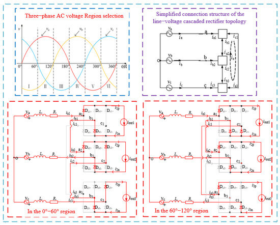
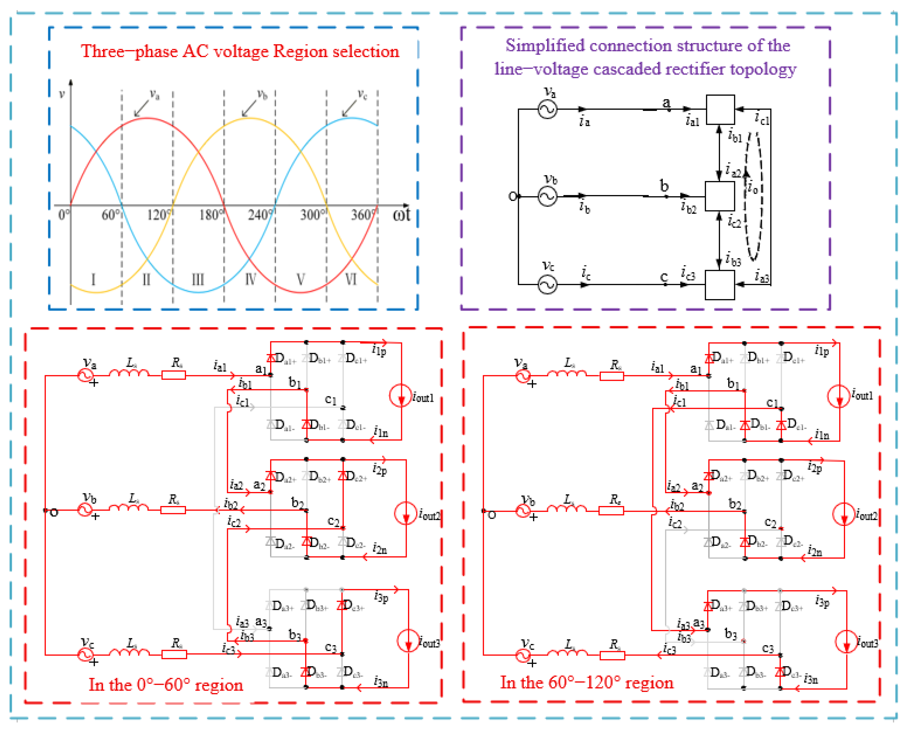
According to the polarity of three-phase voltages, the line-voltage cascaded rectifier is divided into six 60° electrical-angle regions within one power-frequency cycle, each corresponding to a distinct circuit operating mode, as shown in the top-left subgraph of Figure 2. These regions fall into two categories.
Figure 2.
Region division, simplified connection structure and operating modes of line-voltage cascaded rectifier.
In the 0–60°, 120–180° and 240–300° regions, two phases possess higher instantaneous voltages than the third. Taking the 0–60° region as an example, currents in the modules of the two high-voltage phases flow from the AC source to the rectifier, whereas the current of the low-voltage phase module flows back to the source. Reverse-biased diodes block current between the two high-voltage phases. Take the 0–60° region to analyze the conduction path of the proposed topology, as shown in the down-left subgraph of Figure 2. Here, va and vc are positive and vb is negative. Currents of Module 1 va and Module 3 vc flow toward Module 2 vb, with no current between Module 1 and Module 3.
In the 60–120°, 180–240° and 300–360° regions, two phases have lower instantaneous voltages than the third. For the 60–120° region, the module current of the single high-voltage phase flows from the AC source to the rectifier, and currents of the two low-voltage phase modules return to the source. No current conducts between these two low-voltage phases. In the 60–120° region, as illustrated in the down-right subgraph of Figure 2, vb and vc are negative while va is positive. The current of Module 1 va flows into both Module 2 and Module 3, and no current passes between Module 2 and Module 3.
2.2. Circulating-Current and Current-Sharing Characteristics
2.2.1. Derivation of Circulating Current Under Ideal Operating Conditions
Under ideal operating conditions, the three-phase input voltages are perfectly balanced sinusoids, all power modules feature identical circuit parameters and no parameter mismatch exists among the three parallel-connected phase modules. For the line-voltage cascaded rectifier, the phase currents of three modules are determined by the instantaneous line voltages and switching states. Since each phase module shares identical operating duty cycles and conduction sequences within every 60° electrical-angle sector, the currents of three modules can be evenly distributed.
For the simplified connection structure shown in Figure 2, balanced input voltages and loads are maintained among the three-phase modules, yielding identical phases referenced to the source neutral point O. The internal circulating-current loop equations are derived via Kirchhoff’s Voltage Law (KVL). Equation (2), derived from Equation (1), demonstrates zero loop voltage and zero loop current, implying the absence of inter-phase circulating current under ideal operating conditions.
vb1 = va2; vc1 = vb3; vc1 = va3;
ub1c1 = vb1 − vc1; ua3b3 = va3 − vb3; uc2a2 = vc2 − va2;
ub1c1 = vb1 − vc1; ua3b3 = va3 − vb3; uc2a2 = vc2 − va2;
ub1c1 + ua3b3 + uc2a2 = 0;
ia3 + ib1 + ic2 = ia2 + ib3 + ic1;
ia3 + ib1 + ic2 = ia2 + ib3 + ic1;
2.2.2. Zero-Sequence Circulating Current Under Non-Ideal Operating Conditions
In practical engineering applications, grid voltage unbalance and load imbalance originating from mismatched module parameters degrade the performance of the power electronic converter. To facilitate analysis, the non-ideal condition of unbalanced input currents induced by three-phase grid unbalance is equivalent to that caused by unbalanced three-phase loads. Detailed analysis of the branch currents in each module is carried out. Taking the intra-phase current ib1 of one phase as an example, its Fourier decomposition is expressed in Equation (3).
Apart from the fundamental component of ib1, a zero-sequence component exists within the delta loop. Nevertheless, the zero-sequence circulating current is confined to the delta loop and cannot flow into the grid.
2.3. Steady-State Analysis Under Ideal Operating Conditions
The foregoing analysis is carried out subject to the unity-power-factor constraint of input voltage and current.
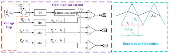
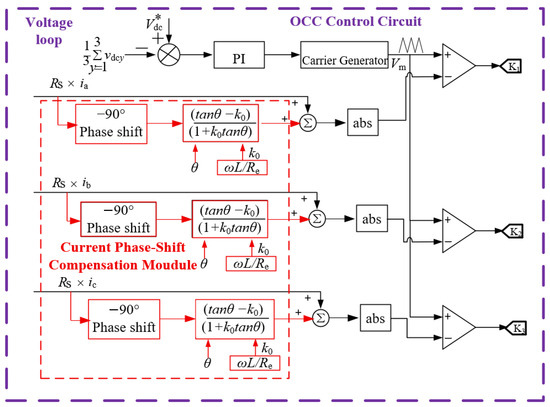
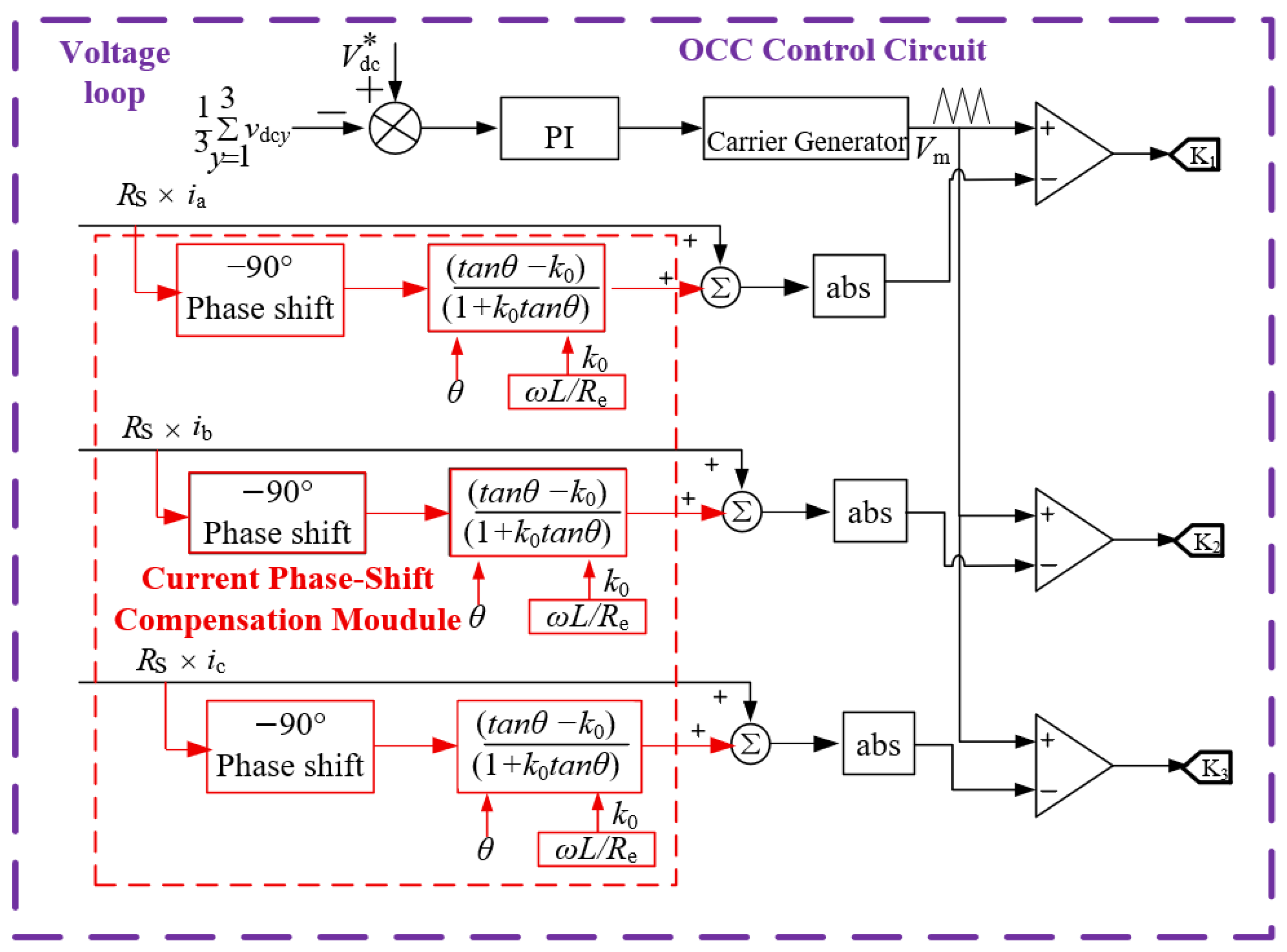
The control circuit section utilizes one-cycle control (OCC) for power factor correction and input current waveform correction, establishing a classic single-loop control configuration: the voltage outer loop computes the mean value of the DC-side output voltage from the three-phase module, compares this value with the reference voltage Vdc*, and subsequently generates a control signal via a PI controller on the left side of the Figure 3 This signal is then transmitted to a carrier generator to produce a triangular carrier signal with a fixed frequency, which serves as the basis for duty cycle modulation. Regarding current control (integrated within the one-cycle control law), the system captures the absolute values of the three-phase current sampling signals ix (where x = a, b, c), multiplies them by the sampling resistor Rs, and thereby derives control signals Rs*ix (where x = a, b, c) that are directly proportional to the current amplitudes. Within the one-cycle control framework, these current signals are directly juxtaposed with the triangular carrier signal to generate the driving pulses K1, K2 and K3 for the switching transistors in each module.
Figure 3.
OCC PFC converter of the one-cycle control strategy.
In contrast to traditional dual closed-loop control, OCC obviates the necessity for an independent current inner-loop controller. Instead, it directly facilitates synchronous tracking of the input current with respect to the grid voltage by ensuring that the average inductor current remains proportional to the input voltage throughout each switching cycle, thereby enabling the system to operate with an approximate unity power factor. Additionally, as demonstrated by the waveform on the right side of the Figure 3, Ref. [1] employs a double-edge modulation strategy. By symmetrically allocating the conduction and cutoff times within the switching cycle, this strategy effectively mitigates current ripple and electromagnetic interference, thereby further optimizing the system’s steady-state performance. This single-loop configuration is characterized by its simplicity in control, rapid dynamic response, and the absence of a requirement for additional voltage sensors, rendering it exceptionally well-suited for application scenarios involving line voltage cascaded three-phase Boost PFC topology.
This operational mode can be equated to a Boost converter subsequent to single-phase voltage rectification, facilitating the decomposition of the three-phase system into three distinct single-phase systems for analytical purposes, thereby markedly streamlining the processes of modeling and control design.
2.3.1. The Steady-State Modal of Novel Topology
The objective of OCC is that, under stable operating conditions of the system, the integral of the current sampling signal at the conclusion of each switching cycle is equivalent to the integral of the input voltage over the duration of the switch’s turn-off period, as shown in Equation (4).
where Rs represents the sampling resistor, Ts denotes the switching period and ton indicates the on-time of the switch. Neglecting the switching ripple effects, we approximate ix(t) as a constant value ix (n) within one switching period, and the variation of Vm(t) within the switching period is minimal, approximating it as Vm(n). Consequently, Equation (4) simplifies to Equation (5).
dx(n) = Ton/Ts indicates the on-duty ratio of the switching device during the nth switching cycle; the fundamental principle of single-cycle modulation is to enforce the fulfillment of the proportional relationship outlined in Equation (6) within every switching cycle.
|ix(t)|Ts = Vm(n)(Ts − Ton),(x = a,b,c)
To investigate the influence of the OCC strategy on the port characteristics of the Boost converter, it is imperative to integrate the control law with the physical constraints inherent in the power circuit. Under the continuous conduction mode of inductor current, the Boost converter adheres to the volt-second balance principle in a steady state, expressed as ux(n) = (1 − dx(n))udcy(n),(x = a,b,c;y = 1,2,3), ux(n), udcy(n), dx(n), which denote the rectifier bridge output voltage, the DC output terminal voltage and the duty cycle of the switch during the nth switching cycle, respectively. This equation elucidates the intrinsic relationship between voltage and duty cycle within the power circuit, which remains unaffected by the control methodology employed. Conversely, the OCC strategy directly establishes the relationship between the duty cycle, input voltage, and output voltage through modulation techniques, referred to as the control law. To reveal the port characteristics of the converter under control action, the control law is substituted into the volt-second balance relation, eliminating the intermediate variable dx(n), and yielding the relationship under the control strategy as shown in Equation (7).
The equation reveals that, under the influence of OCC, the input port of the Boost converter demonstrates purely resistive characteristics, with its equivalent resistance, Re, being dictated by the control parameters and the output voltage. Equation (7) delineates the steady-state model of a three-phase bridge combined with a Boost PFC rectifier operating under OCC. Here, Re signifies the equivalent resistance that mirrors the magnitude of the load power. Under steady-state conditions, provided that the capacitance is adequately large and the bandwidth of the PI controller is relatively constrained, Re maintains a constant value throughout a single power frequency cycle. The input characteristics of the converter inherently adjust the input current in response to variations in the grid voltage. Nevertheless, in practical engineering, to precisely capture the system’s characteristics, the voltage across the inductor must be taken into account when formulating the rectifier model. Consequently, the transfer function between the voltage and current at the input terminal is expressed as follows:
2.3.2. Small-Signal Model of Novel Topology
Drawing upon the derived large-signal state-space averaging model, a linearized small-signal model for the converter is constructed by introducing small-signal perturbations at the system’s steady-state operating point and subsequently applying linearization approximation to the nonlinear terms within the model, as presented below:
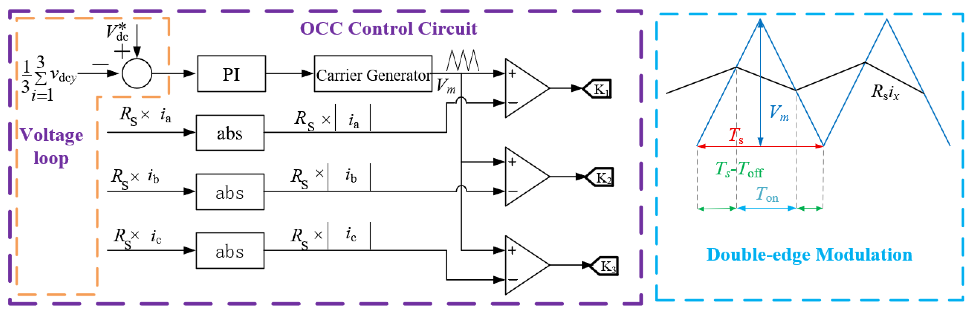
From Equation (9), the small-signal block diagram of the dual-loop structure for the proposed topology rectifier, consisting of an outer DC voltage control loop and an inner OCC current loop, can be derived as shown in Figure 2.
In Figure 4, the region enclosed by the red dashed box represents the equivalent current-loop model. By introducing the concept of current tracking control into the analysis, it reflects the dynamic relationship between the converter’s input voltage and inductor current under OCC, intuitively revealing its operating mechanism. This model maps the output of the voltage controller to the reference command of the input current, clearly demonstrating the current-following objective of OCC.
Figure 4.
Block diagram of small signal system.
Meanwhile, the equivalent current-loop adopts a proportional control structure, whose gain is determined by the equivalent resistance Re. Consequently, the dynamic performance of the current loop is directly related to the system load condition. Additionally, due to the existence of a load disturbance channel in the model, load power fluctuations directly impact the output voltage.
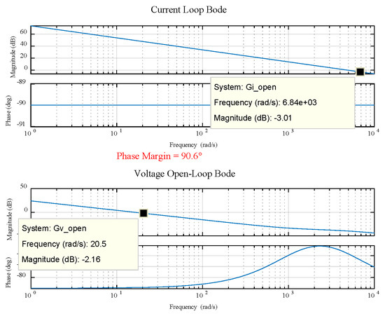
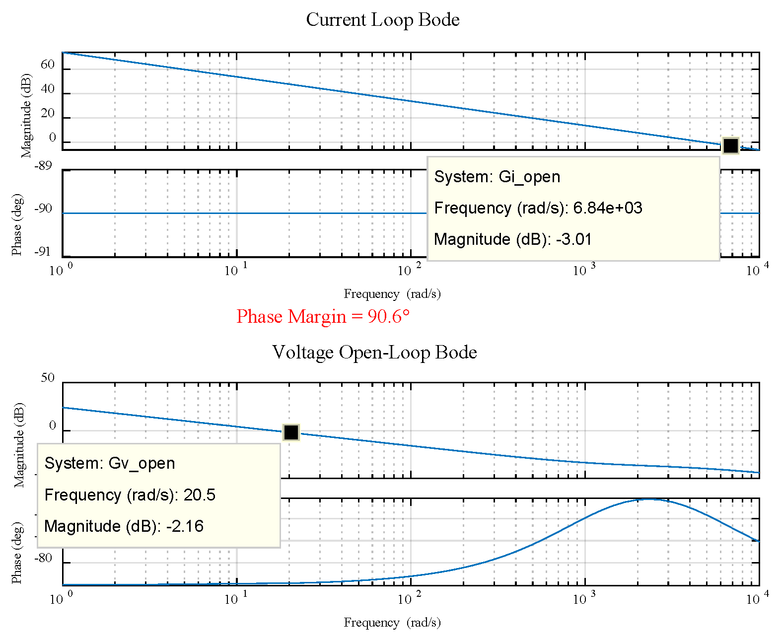
Figure 5 presents the open-loop loop gain Bode diagrams of the current loop and voltage loop derived from the established small-signal model, instead of the transfer function of the plant only. The upper subplot corresponds to the open-loop Bode characteristic of the current loop, while the lower subplot is for the voltage loop.
Figure 5.
Open-loop loop gain Bode diagrams of the current loop and voltage loop based on the small-signal model.
In the time domain, the time constant τ = L/Re indicates that the response of the inductor current to the input voltage represents a first-order inertial process without overshoot. The response speed is determined by L/Re. A heavier load (a smaller Re) leads to a smaller time constant and a faster response. It is a standard first-order inertial element, with a static gain K = 1/Re. Therefore, the system exhibits stronger current tracking capability under heavy-load conditions. In the frequency domain, the first-order inertial element acts as a low-pass filter, with a transition frequency ωc = 1/T = Re/L. Signals below this frequency can pass through with nearly no attenuation, while signals above this frequency experience an amplitude attenuation at a slope of −20 dB/dec, accompanied by a monotonic increase in phase lag from 0° to −90°. This characteristic limits the current tracking bandwidth of the system, which is the fundamental reason for the current phase lagging behind the voltage.
The open-loop Bode plots of the current loop and voltage loop based on the small-signal model are shown in Figure 5. The current loop demonstrates a first-order low-pass characteristic, but its crossover frequency is tracking high-frequency modulation signals. The current phase deviation at zero crossing mainly arises from the combined fundamental-frequency phase lag: the phase shift from the inductor inertial effect and the additional phase lag introduced by digital control delay, rather than insufficient bandwidth or insufficient dynamic response.
3. Current Phase Compensation Mechanism and Phasor Analysis Based on Single Cycle
In a three-phase line-voltage cascaded PFC converter, the existence of the boost inductor leads to the input current lagging behind the grid voltage, giving rise to an inherent phase-shift angle θzeroarctan(L/Re). This lag angle is determined by the fundamental frequency, the boost inductance and the equivalent load resistance, and it increases as the load power increases. This is also the fundamental cause for the converter to externally present inductive reactive characteristics. To realize controllable adjustment of the current phase, this paper puts forward an improved OCC strategy.
By adjusting the phase of the control voltage across the switch, the leading effect of the inductor voltage drop is eliminated, enabling dynamic adjustment from under compensation to full compensation.
3.1. Phasor Relationship Between Inductive Voltage Drop and Switch-Tube Voltage
Based on the inductance volt-ampere characteristic, the grid voltage, inductance current and equivalent control voltage across the switching transistor adhere to the following phasor relationship vx + uL + ut, where the inductance voltage drop leads the current by 90°. This phenomenon is the fundamental cause of the current lagging behind the grid. To counteract this leading component, the control voltage ut at the terminal of the switching transistor must lag behind the current by β. The inductance voltage drop can be partitioned into two parts: the part borne by the control side is and the part borne by the grid side is . Only through the superposition of these two parts can a grid voltage with a controllable phase relative to the current be acquired.
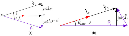
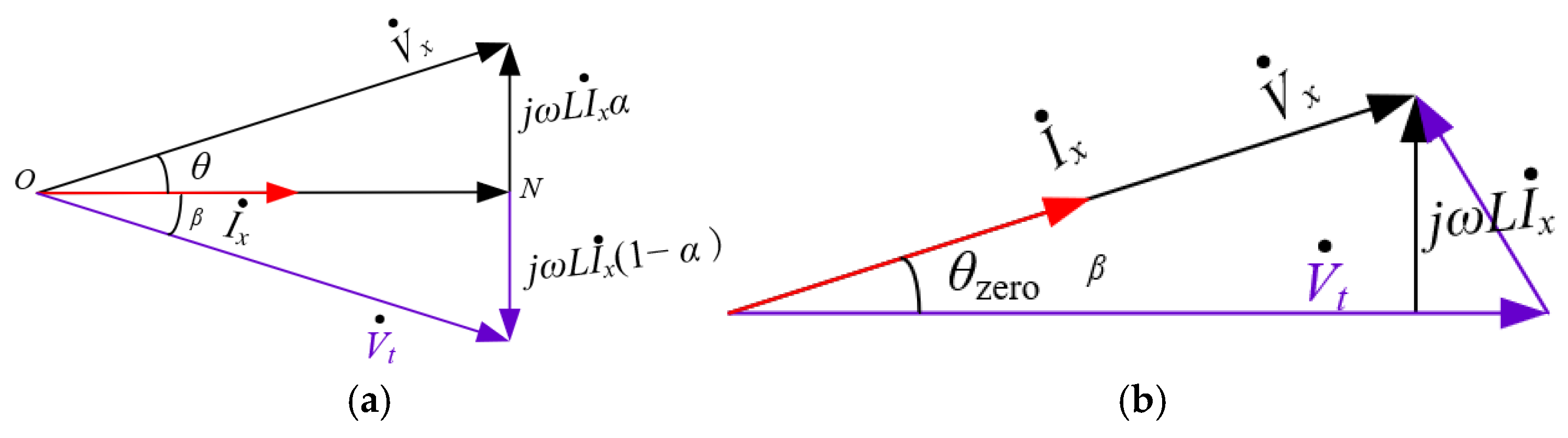
Figure 6 illustrates the phasor diagrams of the power supply voltage and current under various compensation states.
Figure 6.
Phasor diagram of compensated power voltage and current: (a) under-compensation condition; (b) full-compensation condition.
Under the under-compensation condition (Figure 6a), the lag angle of the switch voltage ut is relatively minor. The inductor voltage drop is not completely offset, and the input current still lags behind the grid voltage by an angle θ.
Under the full-compensation condition (Figure 6b), through the adjustment of the phase of the switch modulation signal, the angle by which the switch voltage lags behind the current is fully counteracted by the inductor voltage drop. At this juncture, the input current is in phase with the grid voltage, attaining unity power factor operation.
3.2. Implementation Logic of Current Phase Compensation
From the phasor relationship, it can be observed that the phase of the input current is not solely determined by the grid voltage, but it instead influenced by the combined effect of the grid voltage and the switch voltage. Assuming a specific input power, let θzero denote the inherent angle by which the current lags behind the grid voltage prior to compensation, and β represent the angle by which the switch modulation signal lags behind the current. Then, the lag angle of the compensated current is θ = θzero − β. Through dynamic adjustment of the phase β of the switch modulation signal, the phase of ut can be altered (ut = (1 − d)Udcy), thereby compensating for the current’s lag angle. When β = θzero, θ = 0, resulting in a unity power factor; when β < θzero, the current still lags behind the grid voltage, and the converter externally exhibits inductive characteristics, capable of absorbing reactive power.
To attain the control objective of unity power factor, the impedance equivalent to the voltage across the switching tube demonstrates capacitive characteristics, which counteract the characteristics of the boost inductor within the circuit. The simulated resistor in each phase is transformed from a pure resistor into a complex impedance composed of a resistor and a reactor connected in series, mirroring the reactance necessary for achieving unity power factor operation of the input voltage and current.
Under the premise of a certain input power Pin, let θzero be the angle at which vx lags before compensation ix, and β be the angle at which the control voltage across the switch lags behind ix. Then θ = θzero − β represents the angle at which ix lags behind vx after compensation.
By adjusting the amplitude and phase of ut (the control voltage across the switch), the angle at which ix lags behind vx is reduced, thereby improving the power factor. Figure 6 depicts the compensated power supply voltage and current phasor diagrams. After compensation, the angle at which ix lags behind vx is θ, and the angle at which ut lags behind ix is β. Combining this with Figure 6a, the amplitude and phase of ut can be derived as follows:
Based on Equation (10), it can be inferred that
When θ = 0, by substituting it into Equation (11), we derive β = arctan(ωL/Re) = θzero. This value fully compensates for the angle by which the input current lags behind the power-supply voltage, thereby attaining a unity power factor between the input power supply and the current, as depicted in Figure 6b. Here, β denotes the compensation quantity, and with the increase in β, θ gradually diminishes. When θ < 0, it is termed over-compensation, which may lead to significant distortion at the current zero-crossing point.
4. Improved Control Strategy
Disregarding the angle θ by which the input current lags behind the grid voltage, which is induced by the inductance voltage drop, the OCC system fails to attain unity power factor operation in a genuine sense. The core control equation of its improved OCC system is
In Equation (12), the first term on the right hand side denotes the active component consumed by the load, whereas the second term represents the reactive component consumed by the load. The second term will be employed to compute the phase shift angle of the input current. If Xe (equivalent reactance introduced by the phase compensation control term) in the second term equals zero, the voltage and current at the input terminal of the control system will attain true unity power factor operation. Consequently, Equation (13) can be equivalently presented as
Equation (12) is the general formula with configurable equivalent reactance Xe. Unity power factor can be achieved by setting Xe = −ωL to cancel the inductive term.
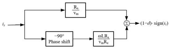
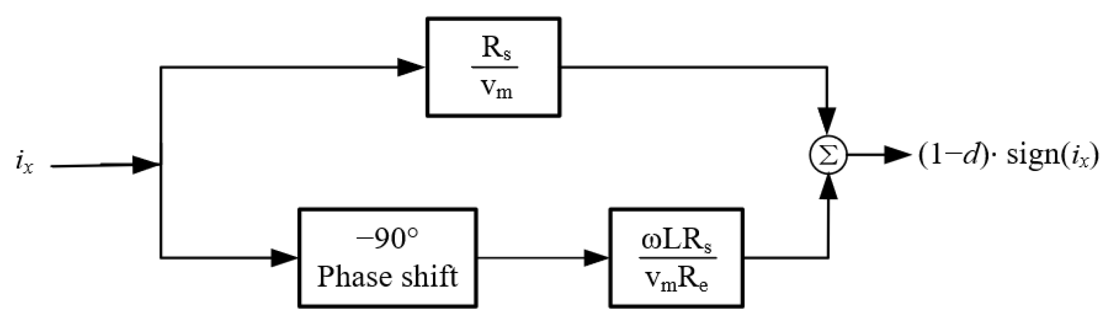
Equation (13) is the practical implementation case with Xe = 0. Instead of adding extra hardware reactance, a–j phase shift is introduced in control algorithm to compensate the current lag caused by filter inductor. Equation (12) serves for theoretical analysis, while Equation (13) is adopted for practical control realization. The signal-flow block diagram of the general control equation described by Equation (13) is shown in Figure 7.
Figure 7.
Signal flow block diagram of the control scheme in Equation (13).
Figure 8 illustrates the control block diagram for lagging phase shift. The sampled current undergoes a −90° phase shift, is multiplied by the reactive power compensation coefficient k and is then superimposed with the current sampling signal to generate the modulation signal for the switch. This allows the voltage across the switch to automatically track the synthesized current signal, thereby establishing the control strategy for the voltage lagging behind the current of the switch.
Figure 8.
Phase−shift control strategy for full compensation and under−compensation hysteresis angles.
The foregoing analysis is predicated on full compensation. However, in the actual design of compensation schemes, the minimum adjustment unit for compensation depth through digital control is typically 0.5Ts, which makes it arduous to guarantee full compensation. To mitigate the fundamental phase shift, it is generally operated in an under-compensation state, with the objective of approximating full compensation as closely as feasible. Consequently, the improved control strategy is devised based on the under compensation scheme. In conjunction with Figure 8, Equation (12) and Equation (13), the modulation signal of the switch transistor lags the sampled current by β, namely, β = θzero − θ. Subsequently, the reactive power compensation k is adjusted to
5. Simulation and Experiment
5.1. Simulation Waveform Under Under-Compensation State
Based on the simulation parameters from the previous section, with a rated load power Pin = 20 kW, Uin = 220 V, L = 2 mH, R1 = 20 and Udc1 = 365 V, the equivalent input impedance Re and the angle β at which the switch terminal voltage ut lags behind ix at unity power factor are respectively
By integrating Equation (15) with Equation (16), the delay time Δt corresponding to β can be computed, and the quantity of switching cycles n corresponding to the delay time is
Consequently, Δt = 3.11Ts, and complete compensation cannot be realized.
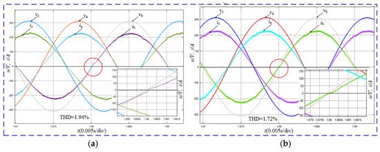
From the simulated experimental waveform of voltage and current in the under-compensation state presented in Figure 9, it can be discerned that the phase θ of the input current lagging behind the power supply voltage diminishes after compensation in comparison to that before compensation. This verifies the efficacy of the compensation method. The total harmonic distortion (THD) of the input current in Figure 9 is less than 5%, which satisfies the requirements of power grid quality.
Figure 9.
Simulation waveform of input voltage and current in lack compensation state (before and after compensation): (a) before compensation; (b) after compensation.
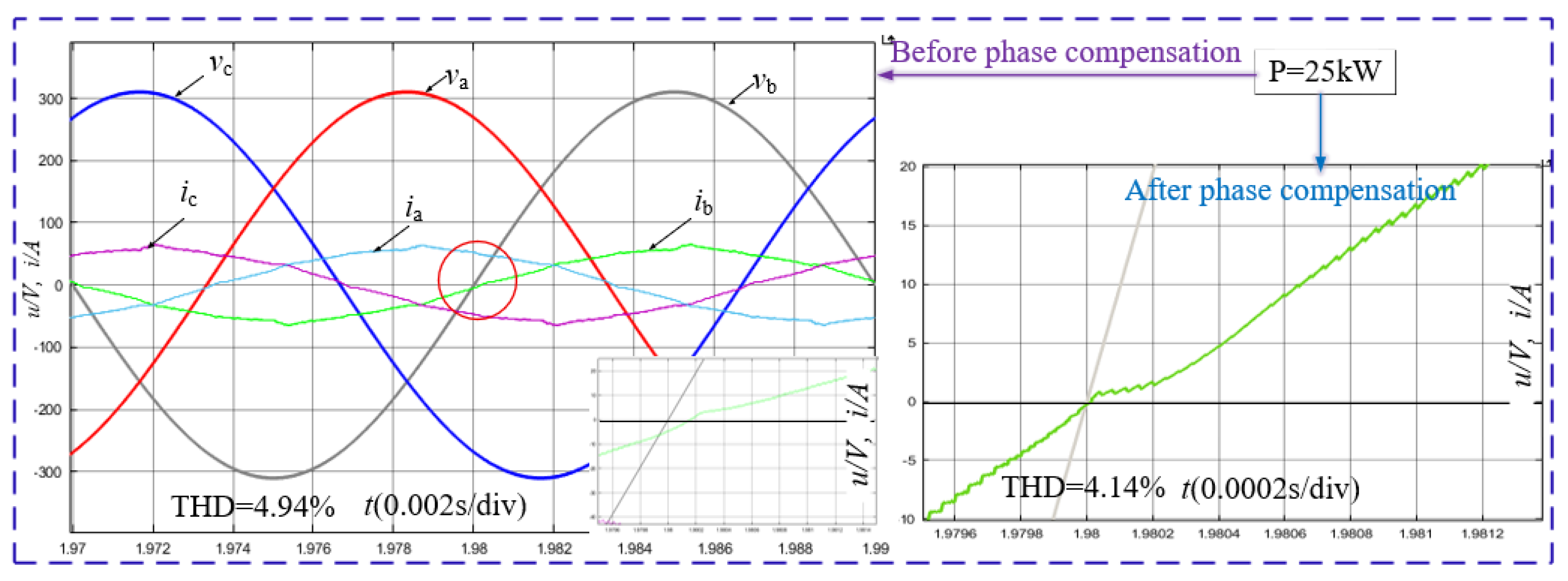
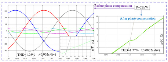
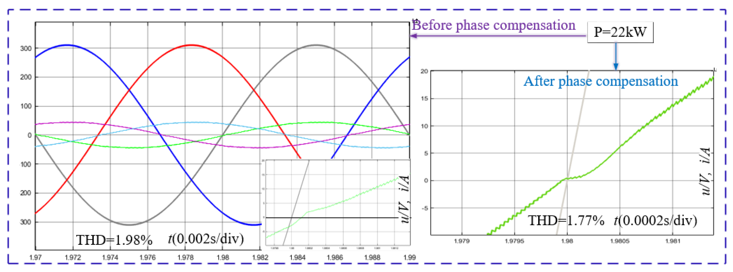
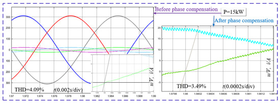
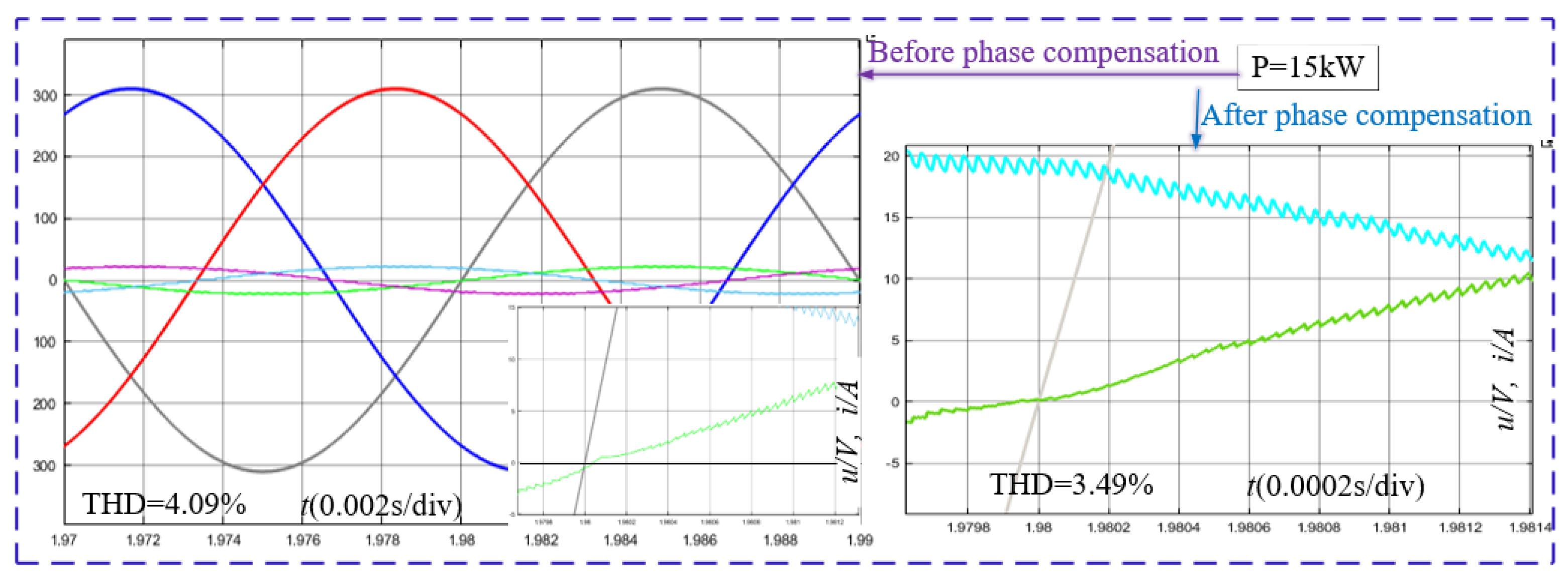
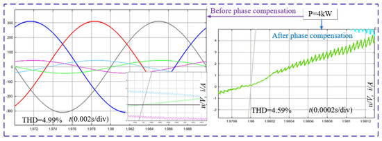
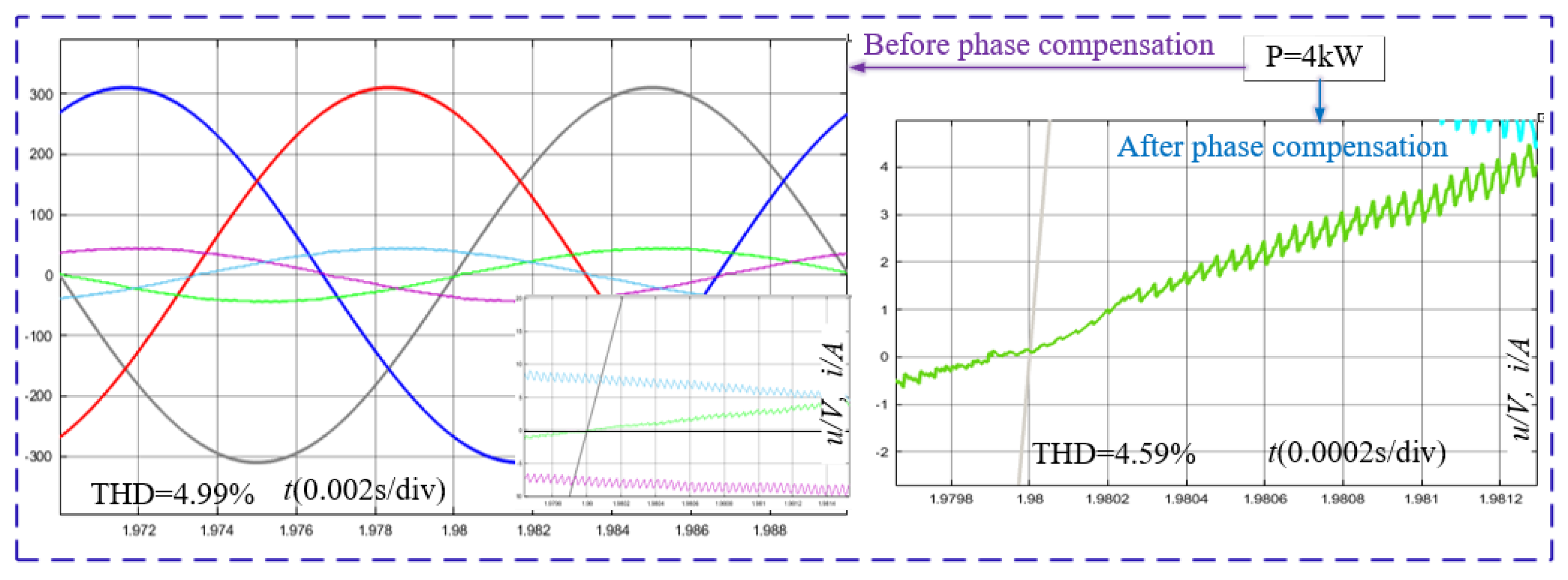
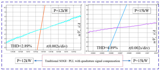
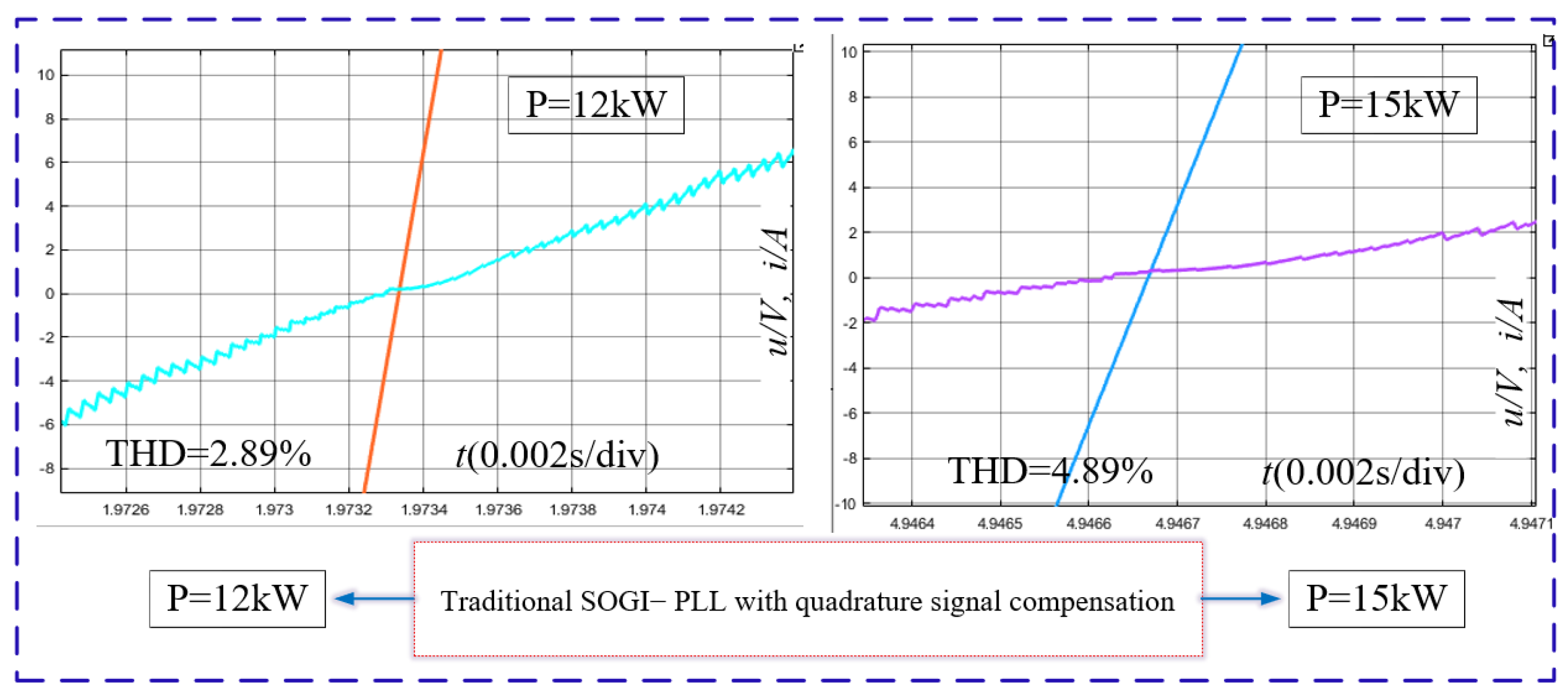
Following the rated-condition analysis above, Figure 10, Figure 11, Figure 12, Figure 13 and Figure 14 present quantitative results under light-load, half-load and heavy-load conditions, comparing the total harmonic distortion (THD) and zero-crossing phase error of three schemes: uncompensated one-cycle control (OCC), the proposed fixed phase compensation method and the conventional SOGI-FPLL quadrature signal compensation scheme as the benchmark. The zero-crossing phase error is defined as the phase difference between the fundamental grid-side current and grid voltage; a positive value means the current leads the grid voltage, and a negative value means the current lags the grid voltage.
Figure 10.
Waveforms before and after phase compensation for OCC under 25 kW condition.
Figure 11.
Waveforms before and after phase compensation for OCC under 22 kW condition.
Figure 12.
Waveforms before and after phase compensation for OCC under 15 kW condition.
Figure 13.
Waveforms before and after phase compensation for OCC under 4 kW condition.
Figure 14.
Waveforms of traditional SOGI-PLL with quadrature signal compensation under 12 kW (right) and 15 kW (left) operating conditions.
Following the rated-condition analysis above, the quantitative results under light-load, half-load and heavy-load conditions, including THD and zero-crossing phase error of the three schemes, are summarized in Table 1.
Table 1.
Comparison of grid-side performance among uncompensated OCC, the proposed fixed phase compensation method and SOGI-PLL orthogonal signal compensation under different load conditions.
5.2. Simulations and Experiments
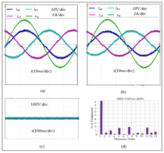
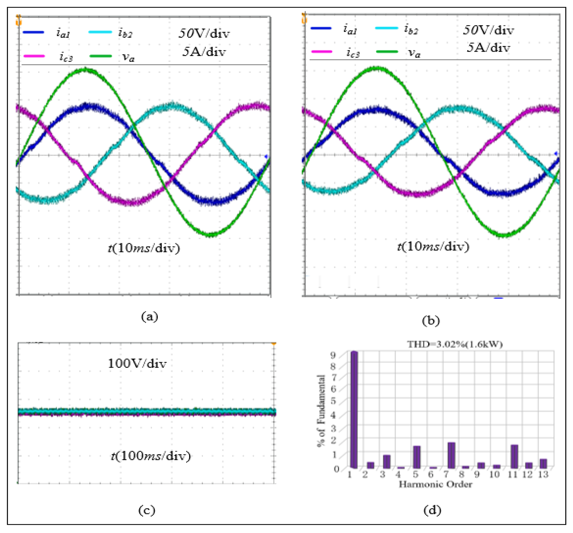
To verify the feasibility of the proposed topology, a 1.7 kW prototype was built, as depicted in Figure 15.
Figure 15.
Waveforms of grid voltage, grid-side current, output voltage and THD before and after phase compensation: (a) before phase compensation; (b) after phase compensation; (c) output voltage; (d) THD (3.02%).
The experimental parameters of the prototype listed as Uin = 110 V, L = 2 mH, R1 = 110 Ω, C = 2200 uF, fs = 10 kHz and Udc = 250 V, FQPF13N50C and Mur1660CD were chosen for the power-switch and fast-recovery diode. A TMS320F28335 DSP was used as the controller.
Figure 15 shows the steady-state waveforms and harmonic spectrum at light load (1.7 kW). Figure 15a,b illustrate the three module currents and phase-A grid voltage before and after the fixed-phase compensation. It can be observed that the zero-crossing distortion of currents is effectively mitigated after compensation, and the phase alignment between grid-side current and grid voltage is improved. Figure 15c depicts the output DC voltage with small ripple and stable magnitude. The harmonic spectrum of grid-side current is given in Figure 15d, where THD is 3.02%, indicating that the harmonic distortion of the rectifier meets relevant power-quality standards under rated operating conditions.
6. Conclusions
This paper investigates the coupling mechanism of zero-crossing distortion originating from input current phase lag and limited current-loop bandwidth under power-frequency grid operation. The input current phase lag leads to desynchronization between current tracking and grid voltage, while insufficient bandwidth fails to cope with fast-voltage transients at zero crossings and exacerbates waveform distortion. A phase compensation strategy is proposed by imposing phase lag on the switch-terminal voltage. By adding a 90° phase-shifted current component to the sampled current, the fundamental phase of the switch voltage is adjusted to produce a modulation signal lagging the input current. This scheme regulates the input current phase and reduces the fundamental phase difference between grid voltage and current to mitigate waveform distortion. The adopted reference current phase-lead method compensates the inherent current phase lag, enhances the tracking performance for zero-crossing transients and suppresses zero-crossing distortion effectively. Moreover, the studied topology inherently restricts zero-sequence circulating current within the delta loop and avoids injecting such circulating current into the grid under non-ideal operating conditions, and the proposed phase compensation scheme does not compromise this feature. Simulations and experiments validate the feasibility of the improved strategy.
Author Contributions
Conceptualization, X.L. (Xia Liu) and H.Y.; methodology, X.L. (Xia Liu), Y.X. and K.W.; validation, X.L. (Xia Liu), H.Y., J.D. and K.W.; formal analysis, X.L. (Xiujie Liu) and Y.X.; writing—original draft preparation, X.L. (Xia Liu); writing—review and editing, X.L. (Xia Liu) and H.Y.; visualization, Y.X. and J.D.; funding acquisition, Y.X., X.L. (Xiujie Liu) and K.W. All authors have read and agreed to the published version of the manuscript.
Funding
This work was supported by the Sailing program of Yibin University under project 2023QH24. This work was supported by the Sichuan Provincial Department of Science and Technology, Sichuan Provincial Key R&D Program, 2021YFG0199. This work was supported by the Tai’an Science and Technology Innovation Development Project, 2023GX069.
Data Availability Statement
All relevant simulation data are included within the article. Additional raw simulation files are available from the corresponding author on reasonable request.
Conflicts of Interest
The authors declare that the research was conducted in the absence of any commercial or financial relationships that could be construed as a potential conflict of interest.
References
- Eswaraiah, B.; Balakrishna, K. A novel on high voltage conversion ratio DC-DC converter for EV-fed fuel cell application with hybrid MPPT controller. Int. J. Circuit Theory Appl. 2023, 52, 1962–1993. [Google Scholar] [CrossRef] [Scilit]
- Farhadi-Kangarlu, M.; Khiavi, A.M.; Neyshabouri, Y. Analysis and suppression of switching-frequency harmonics in variable-output-voltage inverters. Int. J. Circuit Theory Appl. 2023, 52, 2403–2420. [Google Scholar] [CrossRef] [Scilit]
- Tong, M.; Cheng, M.; Hua, W.; Ding, S. A Single-Phase On-Board Two-Stage Integrated Battery Charger for EVs Based on a Five-Phase Hybrid-Excitation Flux-Switching Machine. IEEE Trans. Veh. Technol. 2020, 69, 3793–3804. [Google Scholar] [CrossRef] [Scilit]
- Wang, C.; Liu, X.; Li, Z.; Cheng, H.; Chen, T.; Kong, J. Novel high-power triple line-voltage cascaded unity power factor rectifier. J. Power Electron. 2023, 23, 89–101. [Google Scholar] [CrossRef] [Scilit]
- Wang, C.; Liu, X.; Cheng, H.; Kong, J.; Chen, T. Research on static characteristics and output voltage balance control of a novel line-voltage cascaded three-phase unity power factor (UPF) rectifier under unbalanced load. Trans. China Electrotech. Soc. 2024, 39, 525–540. [Google Scholar]
- Shan, L.; Wutong, H.; Qiang, G.; Wei, L. Sliding Mode Control Strategy for VIENNA Rectifier Under Unbalanced Grid Voltage Conditions. J. Power Supply 2020, 20, 52–61. [Google Scholar]
- Zou, Y.; Zhang, L.; Xing, Y.; Zhang, Z.; Zhao, H.; Ge, H. Generalized Clarke transformation and enhanced dual-loop control scheme for three-phase PWM converters under the unbalanced utility grid. IEEE Trans. Power Electron. 2022, 37, 8935–8947. [Google Scholar] [CrossRef] [Scilit]
- Fu, C.; Zhang, C.; Zhang, G.; Zhang, C.; Su, Q. Finite-Time Command Filtered Control of Three-Phase AC/DC Converter Under Unbalanced Grid Conditions. IEEE Trans. Ind. Electron. 2023, 70, 6876–6886. [Google Scholar] [CrossRef] [Scilit]
- Zhang, Y.; Wang, Z.; Jiao, J.; Liu, J. Grid-Voltage Sensorless Model Predictive Control of Three-Phase PWM Rectifier Under Unbalanced and Distorted Grid Voltages. IEEE Trans. Power Electron. 2020, 35, 8663–8672. [Google Scholar] [CrossRef] [Scilit]
- Song, J.; Duan, B.; Fu, C.; Ding, W.; Li, X.; Zhang, C. Nonlinear Backstepping Control Strategy for High-frequency Link Matrix Converter Under Unbalanced Grid Conditions. Proc. CSEE 2022, 23, 761–771. [Google Scholar]
- Panprasert, D.; Neammanee, B. The d and q Axes Technique for Suppression Zero-Sequence Circulating Current in Directly Parallel Three-Phase PWM Converters. IEEE Access 2021, 9, 52213–52224. [Google Scholar] [CrossRef] [Scilit]
- Pan, Z.; Yang, X.; Zhao, R.; Cui, C.; Zheng, T.Q. DC Circulating Current Balancing Control of Modular Multilevel Converter Under Unbalanced Power Grid. Trans. China Electrotech. Soc. 2024, 39, 514–553. [Google Scholar]
- Yue, Y.; Liu, F.; Jiang, W.; Wang, J.; Zhang, Q. The Control and Current Over-Zero Distortion Suppression Method for Vienna Rectifier Under Unbalanced Grid Voltage Condition. Proc. CSEE 2023, 43, 6395–6407. [Google Scholar]
- Cheng, H.; Kong, J.; Wang, X.; Wang, P.; Chen, T.; Wang, C. Power factor adjustment and input current distortion mitigation for three-phase unidirectional rectifier. IET Power Electron. 2019, 12, 1816–1824. [Google Scholar] [CrossRef] [Scilit]
- Jung, K.; Suh, Y. Analysis and Control of Neutral-Point Deviation in Three-Level NPC Converter Under Unbalanced Three-Phase AC Grid. IEEE Trans. Ind. Appl. 2019, 55, 4944–4955. [Google Scholar] [CrossRef] [Scilit]
- Lin, H.; Yan, Z.; Meng, X.; Xie, D. Detection-free neural DC-link voltage correction for cyber-resilient solid-state transformers: A dual-stream denoising scheme. IEEE Trans. Power Electron. 2026, early access. [Google Scholar] [CrossRef] [Scilit]
- Ohn, S.; Phukan, R.; Dong, D.; Burgos, R.; Boroyevich, D.; Gopal, M.; Nielebock, S. A Scalable Filter Topology for N-Parallel Modular Three-Phase AC–DC Converters by an Arrangement of Coupled Inductors. IEEE Trans. Power Electron. 2022, 37, 13358–13367. [Google Scholar] [CrossRef] [Scilit]
- Sun, J. On the zero-crossing distortion in single-phase PFC converters. IEEE Trans. Power Electron. 2004, 19, 685–692. [Google Scholar] [CrossRef] [Scilit]

Disclaimer/Publisher’s Note: The statements, opinions and data contained in all publications are solely those of the individual author(s) and contributor(s) and not of MDPI and/or the editor(s). MDPI and/or the editor(s) disclaim responsibility for any injury to people or property resulting from any ideas, methods, instructions or products referred to in the content. |
© 2026 by the authors. Licensee MDPI, Basel, Switzerland. This article is an open access article distributed under the terms and conditions of the Creative Commons Attribution (CC BY) license.