


Abstract
This paper proposes a double-corrugated waveguide with wide grating (DCWWG) slow-wave structure and applies it to the design of a low-voltage terahertz traveling-wave tube (TWT). To improve the TWT’s efficiency, a phase-tapered slow-wave structure is proposed. A response surface model is developed to identify the optimal tapering scheme, which is then further optimized using a genetic algorithm. Within the frequency range of 205–235 GHz, the phase-tapered DCWWG TWT exhibits significantly higher saturated output power and gain compared to the uniform DCWWG TWT. The maximum output power of the phase-tapered DCWWG TWT reaches approximately 26 W, representing an increase of about 47% over the 19 W maximum output power of the uniform DCWWG TWT. Overall, the phase taper technique substantially enhances the output performance of the DCWWG TWT.
1. Introduction
Terahertz traveling-wave tubes (TWTs) are vital vacuum electronic sources of terahertz radiation, offering both high power and broadband operational capabilities. They hold significant potential for applications in millimeter-wave radar systems, satellite communication systems, and other fields [1,2]. To meet these demands, the miniaturization of TWTs has become increasingly important. However, the excessively high operating voltage of TWTs remains a key factor limiting their miniaturization [3]. For instance, the typical operating parameters of the G-band folded waveguide TWT are 22.4 kV, 58 mA, and a maximum output power of 62.5 W [4], while the typical operating parameters of the Sine Waveguide TWT are 22.4 kV, 80 mA, and a maximum output power of 58 W [5]. Typical operating parameters for a staggered double-grating TWT are 20 kV, 100 mA, and 56 W. Such high voltage requires a power supply measuring about 1.5 m × 0.5 m × 0.5 m, which is considerably larger than the TWT itself [3]. The largest core component in a high-voltage power supply is the transformer, whose volume is proportional to the product of the core cross-sectional area and the window area. When the operating voltage is reduced by 50% from 15 kV, both the core cross-sectional area and the number of winding turns can be reduced to about 50% of their original values. Theoretically, the volume of the new transformer can be reduced to 25% of its original volume. Therefore, in scenarios such as satellites where installation space is strictly limited, reducing the power supply voltage is a core development requirement. Moreover, in slow-wave structures at the micrometer scale, high voltage can generate excessively strong local electric fields, leading to issues such as vacuum breakdown, surface discharge, and structural damage [6]. Therefore, developing low-voltage terahertz TWTs is crucial for achieving system miniaturization, enhancing engineering application capabilities, and improving competitiveness relative to solid-state terahertz sources.
As operating frequencies continue to advance into the terahertz band, the fabrication and assembly of slow-wave structures (SWSs) have become bottlenecks hindering the practical realization of terahertz devices [7]. Traditional helical SWSs and coupled-cavity SWSs are nearly impossible to fabricate and assemble at terahertz frequencies [2]. Staggered double-grating SWSs and other designs suitable for strip-beam electron beams often face technical challenges, including stringent assembly accuracy requirements and Diocotron instability [8,9]. Consequently, developing a terahertz SWS that combines the ease of fabrication and assembly with compatibility for low-voltage cylindrical electron beams is a research area warranting in-depth investigation.
Due to its convenient fabrication and assembly, as well as its excellent properties—such as its suitability for interaction with cylindrical electron beams—the double-corrugated waveguide slow-wave structure has been applied in plasma diagnostics and satellite communications [10,11,12,13,14]. This paper proposes a double-corrugated waveguide with a wide grating slow-wave structure based on the conventional double-corrugated waveguide slow-wave structure. This new structure retains the advantages of the DCW structure, including the ease of fabrication and assembly, and can operate at a lower voltage. Building on this structure, we designed a two-section TWT and introduced a phase taper structure to improve interaction efficiency.
This paper is organized as follows: Part 2 introduces the frequency characteristics of the slow-wave structure; Part 3 completes the design and optimization of two low-voltage TWTs based on DCWWG SWS; Part 4 constructs a quadratic polynomial response surface for output power, determines the phase taper scheme, and uses a genetic algorithm for further optimization, finally comparing the performance of the phase-tapered TWT and the uniform DCWWG TWT; Part 5 is the summary and research conclusions of the entire paper.
2. Double-Corrugated Waveguide with Wide Grating Slow-Wave Structure
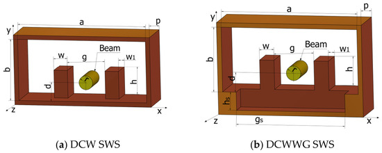
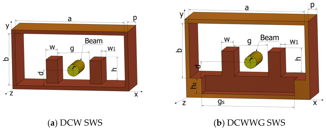
The double-corrugated waveguide slow-wave structure (DCW SWS) is illustrated in Figure 1a, and it comprises two main components: (1) a channel waveguide with two rows of pillars defining the beam channel, and (2) a lid that seals the structure [15]. The first component can be fabricated using deep X-ray LIGA technology. Notably, the waveguide’s length (a) and height (b) have minimal influence on the electromagnetic parameters, which significantly reduces the difficulty of fabrication and assembly. The all-metal construction further facilitates manufacturing, assembly, and heat dissipation, effectively addressing the stringent challenges associated with terahertz (THz) device production. A typical double-corrugated waveguide with a wide grating slow-wave structure (DCWWG SWS) is shown in Figure 1b. Integrating a wide-slot design into the double-corrugated waveguide enhances the longitudinal electric field within the central electron beam channel. Thanks to its excellent electromagnetic properties—such as its high interaction impedance and a more uniform longitudinal electric field—this structure has been utilized in the design of backward-wave oscillators [16]. Additionally, it maintains the advantages of the standard DCW SWS, including insensitivity to dimensional variations and assembly misalignments, which are critical for terahertz frequency applications. This paper optimizes the structural parameters to enable the application of this structure in the design of low-voltage traveling-wave tubes (TWTs).
Figure 1.
Slow- wave structure and electron beam.
In the DCWWG SWS, parameters such as the height (h) and period (p) of the bimetallic pillars play a crucial role in determining core performance metrics, including the operating frequency. Once the operating frequency and voltage are set, the allowable ranges for (h) and (p) become largely fixed, leaving little room for significant adjustment. However, by incorporating a wide-slot design, the DCW SWS achieves increased interaction impedance and a substantially reduced phase velocity, which in turn enables a significant reduction in operating voltage.
Ignoring the role of the two rows of metal posts for the moment, the base of the DCW can be treated as an ideal conducting plane. On the surface of an ideal conductor, the tangential electric field is zero and the surface impedance Zs is 0; consequently, the surface cannot support tightly bound TM surface waves. Therefore, electromagnetic waves propagating along a smooth metal surface behave essentially like free-space waves, with a phase velocity approaching the speed of light. When periodic grooves are etched into the metal surface, TM-polarized waves propagating along the surface—with their magnetic fields aligned with the grooves—encounter a structure where each groove acts as a short-circuited, sub-wavelength parallel-plate transmission line. The field within the groove is shorted at the bottom, creating an input impedance at the aperture. For a one-dimensional array of rectangular grooves, the following approximation holds:
where gs is the slot width, p is the period, hs is the slot depth, and η0 is the free-space wave impedance, . When , , so Zs is inductive. The current path along the groove walls is lengthened, and the magnetic energy stored within the groove increases, which is equivalent to an additional inductance. Inductive surfaces support TM surface waves, and their dispersion relation is approximately given by:
When electromagnetic waves propagate along a metal surface, a portion of the energy enters the periodic grooves and reflects back and forth within them, effectively lengthening the propagation path. Simultaneously, the magnetic energy storage within the grooves increases, manifesting as inductive loading. Consequently, the electromagnetic waves are confined near the surface; the external field decays exponentially, and phase accumulation along the surface accelerates—meaning the wavenumber component kx increases and the phase velocity decreases.
Similar to the operating principle of “spoof surface plasmon slow-wave structures (SSP SWSs)” [17], the introduction of periodic grooves into the bottom metal plane modifies the electromagnetic boundary conditions at the surface. This geometric modification induces surface electromagnetic modes analogous to SSP. The presence of these slots significantly lowers both phase and group velocities; deeper grooves lead to stronger confinement of electromagnetic waves, a more pronounced slow-wave effect, and consequently, a lower operating voltage for the traveling-wave tube. At the same time, this enhances the surface wave effect near the bottom region, thereby increasing the interaction impedance there. Interaction impedance is a key parameter for evaluating the interaction performance of SWSs [18].
where is the longitudinal electric field amplitude of the first positive spatial harmonic at the corresponding point in the electron beam channel, is the single-cycle phase shift of the first positive spatial harmonic at a specific frequency, P is the total power flow through the periodic system, and Se is the cross-sectional area of the SWS.
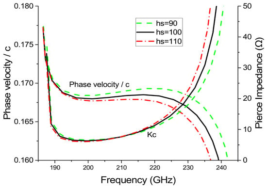
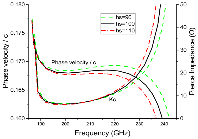
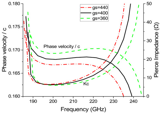
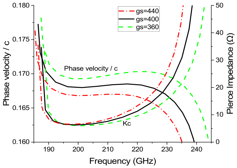
A DCWWG model was developed using CST STUDIO SUITE to investigate the effects of variations in slot width (gs) and slot depth (hs) on the phase velocity and interaction impedance of the slow-wave structure. As shown in Figure 2, a 10% increase in slot depth (hs) results in an increase in coupling impedance and a decrease in phase velocity. The impact of variations in slot width (gs) on phase velocity is more pronounced; as illustrated in Figure 3, a 10% increase in slot width (gs) significantly increases the coupling impedance and substantially decreases the phase velocity.
Figure 2.
The influence of slot depth hs on phase velocity and interaction impedance of DCWWG SWS.
Figure 3.
The effect of slot width variation gs on phase velocity and interaction impedance of DCWWG SWS.
The introduction of wide grating enhances the adjustable parameters of the SWS, enabling the SWS to operate at a lower voltage. The optimized parameters of the DCWWG SWS are presented in Table 1.
Table 1.
Parameters of DCWWG SWS.
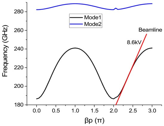
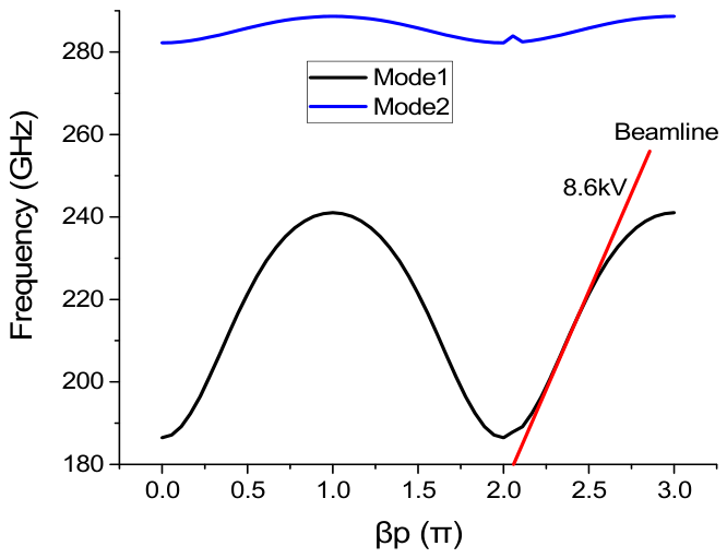
The dispersion characteristics of the SWS are illustrated in Figure 4. To reduce the operating voltage, we selected the +1 harmonic for operation. To suppress interference from other modes and prevent oscillations, it is essential to maintain a wide stopband between the operating mode and adjacent modes; consequently, there is a significant frequency gap between Mode 1 and Mode 2. In the region near 2π to 3π, the dispersion curve aligns with an electron beam at a voltage of 8.6 kV, enabling effective interaction between the SWS and the electron beam.
Figure 4.
Dispersion curve of DCWWG SWS.
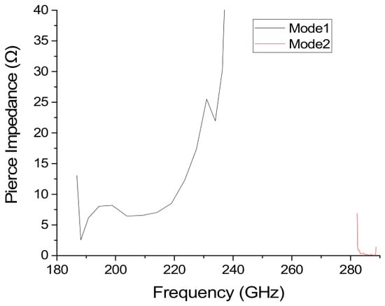
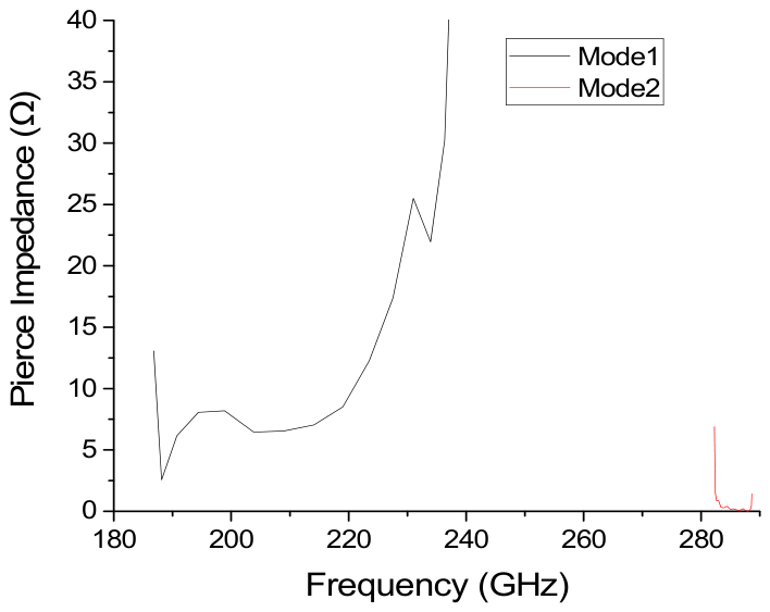
At this point, the interaction impedances of Mode 1 and Mode 2 are presented in Figure 5. It can be observed that there is not only a sufficiently wide stopband between Mode 1 and Mode 2, but the interaction impedance of Mode 2 is also significantly lower than that of Mode 1. Therefore, in subsequent analyses, the impact of Mode 2 on Mode 1 is expected to be relatively small.
Figure 5.
Interaction impedance of DCWWG SWS.
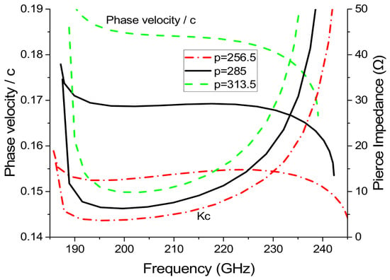
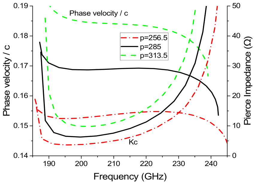
When all other parameters remain constant, altering the period (p) of the SWS can effectively adjust its phase velocity. As shown in Figure 6, a 10% increase in the period (p) results in a significant decrease in the overall phase velocity and an increase in bandwidth within the operating frequency range. Subsequently, we will induce a by modifying the period (p), thereby enhancing the power output of the traveling-wave tube.
Figure 6.
The influence of periodicity p on phase velocity and interaction impedance of DCWWG SWS.
3. Design and Optimization of a Two-Section Traveling-Wave Tube
This section presents the design of a two-section traveling-wave tube based on the double-corrugated waveguide with wide grating slow-wave structure (DCWWG SWS). We determines the number of periods for each section, and optimize the transmission characteristics of the traveling-wave tube (TWT).
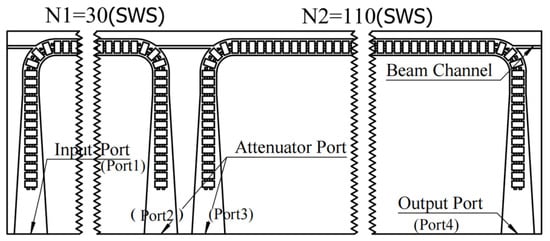
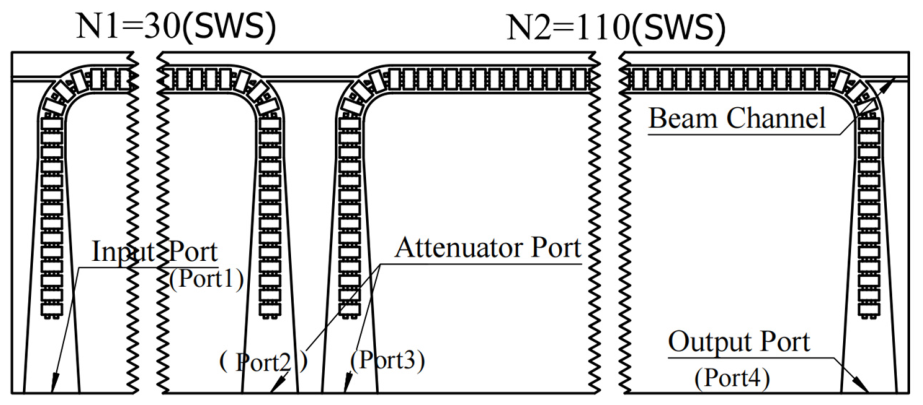
TWTs experience internal reflections (e.g., window mismatch, inhomogeneous slow-wave structure), causing waves to feed back to the input. When phase and gain conditions are met, self-oscillation occurs. To suppress this back-wave oscillation, a sever (truncated structure) is introduced, forming a two-section TWT structure. The input–output coupler employs a linear transition structure. In the transition segment, the double rows of metal pillars and the slot depth decrease arithmetically to zero, while the waveguide height remains constant, and the waveguide width gradually increases until it connects with the standard waveguide. The TWT structure based on the DCWWG SWS is shown in Figure 7. The two-section TWT achieves a complete physical disconnect between the first and second segments, improving the device’s gain stability. This structure can be fabricated in a single step, reducing the difficulty of fabrication and assembly.
Figure 7.
Cross-sectional view of a uniform traveling-wave tube.
The primary objective of the first stage is not to achieve high output power but to efficiently pre-modulate the electron beam. Therefore, the number of periods, N1, in the slow-wave structure (SWS) of the first stage is set to 30. The main goal of the second stage is to convert the kinetic energy of the electron beam into high-power microwave energy output. To determine the number of periodic structures in the second segment, we studied the relationship between the period length of the second segment and the output power while keeping the period length of the first segment constant. The results showed that the output power reached its maximum when the number of periods reached 110; further increasing the number of periods resulted in a slight decrease in output power. Therefore, we determined the number of periods for the second SWS to be 110.
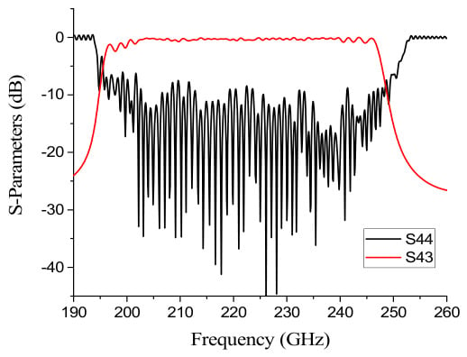
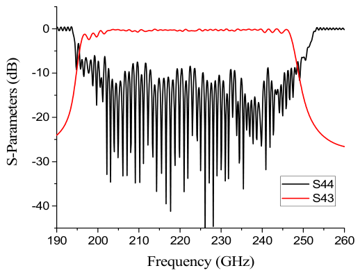
The optimized S-parameters of the second stage are shown in Figure 8. The optimized S44 is less than −10 dB, which reduces reflection interference at the output end on the electron beam inside the tube and improves output efficiency.
Figure 8.
S-parameters of the second segment of the traveling-wave tube.
4. Performance Optimization of TWT Based on Phase Taper Technology
For the two-section uniform traveling-wave tube (TWT) in Figure 6, this paper introduces a DC electron beam in the CST-PS simulation environment. The electron beam voltage is set to 8.6 kV, the electron beam current to 0.1 A, the input signal frequency to 220 GHz, the input signal power to 0.125 W, and the conductivity of the boundary conditions to 3 × 10⁷ S/m, the uniform magnetic field along the direction of the electron beam is 0.6 T.
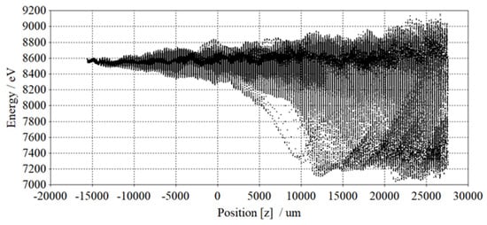
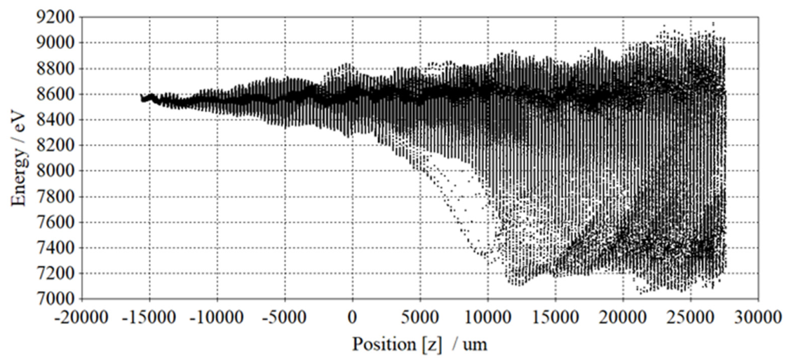
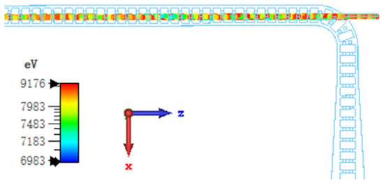
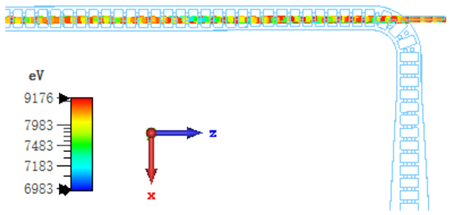
After the DCWWG TWT output stabilizes, the electron energy distribution along the z-axis is shown in Figure 9. Simulation results show that in the terminal region of the slow-wave structure of the TWT, a large number of electrons decelerate, and their kinetic energy is converted into electromagnetic field energy.
Figure 9.
Electron energy distribution along the z-axis of a TWT.
4.1. Response Surface Methodology for Phase Taper Scheme
To further improve the output power and efficiency of the TWT, we introduced a slow-wave structure with a phase-velocity jump. By changing the geometric dimensions of the slow-wave structure (SWS) in the TWT’s output section, the phase velocity of the electromagnetic field is altered. As a result, the electron beam—after being decelerated or accelerated—re-enters the retarding field of the electromagnetic wave, achieving what is known as “secondary synchronization.”
The phase-velocity jump should be positioned before the electron beam reaches saturation; we chose to implement it between the 101st and 110th periods. Due to the large number of variables, we initially set the parameter (p) to 285 and used a genetic algorithm to optimize it within a ±10% range over 500 iterations. However, this method was computationally demanding, and the resulting configurations were often illogical or erratic. For example, many solutions featured abrupt phase-velocity jumps between adjacent periods, which tend to cause reflections and subsequent oscillations.
To enhance optimization efficiency, we developed a response surface methodology (RSM) model focused on output power and integrated boundary condition analysis to establish preliminary design principles and schemes. Ultimately, we employed a genetic algorithm to determine the optimal configuration within a defined parameter range [19].
Let the period length Xi of the slow-wave structure be the main adjustment parameter,
then we have:
Two response equations are constructed for output power.
Since there are many variables (10 of them), Y is represented by second-order polynomials:
After generating 200 sets of sample data using the Latin hypercube sampling method, the data were imported into the Particle-in-Cell (PIC) module of CST software for simulation to obtain the corresponding output power results. Subsequently, linear regression analysis was conducted on these 200 sample sets.
According to the marginality principle in statistics, if the regression coefficient of an interaction term between independent variables (e.g., X1 × X2) is statistically significant, then the corresponding lower-order main effect terms X1 and X2 must be retained in the regression model regardless of whether their individual p-values reach the significance threshold. In accordance with this principle, the present study includes the main effect terms for the independent variables X1 through X10 in the initial stage of the regression analysis. Subsequently, stepwise regression is employed in the second stage to select interaction terms (e.g., X1 × X2, X1 × X3) and quadratic terms (e.g., X12, X22). Variables are entered into the model if their significance level is (p < 0.05) and removed if (p > 0.05). The significance levels and corresponding regression coefficients of the final polynomial model are presented in Table 2.
Table 2.
Significance tests and coefficients for each term in the regression equation.
Based on Table 2, we can obtain the corresponding regression equation as follows:
Using the hypercube method, 20 data points were generated within the range X ∈ [−30, 30] and used for simulation in CST’s PIC solver. The results were then compared with the predicted values Y obtained from Equation (8). The resulting Root Mean Square Error (RMSE) was lower than that from the 200-run experiment, indicating that the regression equation represented by Equation (8) is valid.
Table 2 indicates that the variable X1 exerts a significant positive influence on the output power Y (p < 0.05), with a coefficient of 0.326, which is relatively substantial. Consequently, this parameter is critical, and X1 should assume a positive value, corresponding to an increase in the period length of p101. In contrast, the variable X2 does not significantly affect the output power Y (p > 0.05), and its influence is minimal. The variable X5 demonstrates a significant negative effect on the output power Y (p < 0.05), with a negative coefficient; thus, X5 should be negative, implying that the period length of p105 should be less than 285 μm. Notably, X10 exhibits the strongest negative impact on the output power Y. Reducing the output period (thereby decreasing the phase velocity) is essential for synchronizing with the decelerated electrons and maximizing the extraction of residual kinetic energy. Regarding the interaction term X1 X3 (coefficient = −0.006, p = 0.000), when X1 increases, X3 must decrease to yield a positive combined effect. This suggests that X3 should reduce the phase velocity of the slow-wave structure as rapidly as possible to maintain synchronization. Finally, the quadratic term has a small coefficient, indicating a relatively minor effect.
In summary, at the initial change position (p101), the phase velocity should be substantially increased (strong positive effect) to achieve maximum velocity modulation of the electron beam. During the transition clustering phase (p102–p104), the clustering phase must be carefully adjusted to maintain the optimal state of the electron beam for subsequent transduction. In the energy extraction phase (p105–p110), the phase velocity should be progressively decreased, culminating in a significant reduction (strong negative effect).
To mitigate issues such as reflections resulting from significant phase velocity discontinuities, the amplitude of the periodic variation must be limited. Specifically, the maximum variation amplitude of X is restricted to no more than 10% of the period length of the uniform SWS, and the variation in the period length between adjacent SWSs is constrained to no more than 2%, as expressed by:
Under the constraints, the values of each period length corresponding to the maximum value of Y are shown in Table 3.
Table 3.
The periodic variation value of each SWS in the TWT phase taper segment.
4.2. Further Optimization Using a Genetic Algorithm
By substituting the parameters from Table 3, the optimal period lengths for p101–p110, as predicted by the Response Surface Methodology (RSM), and the corresponding actual output power obtained from the particle-in-cell (PIC) simulation are presented in Table 4. At an input frequency of f = 220 GHz, the actual output power for this configuration is P = 17.8 W. Although this value remains considerably lower than the predicted maximum output power (Ymax = 25.2 W), it surpasses the output power of approximately 90% of the sampled combinations.
Table 4.
The period of each slow-wave structure in the phase taper segment of the TWT.
For further optimization, the predicted value was employed as the initial value, with a variation range of ±3% applied to each initial parameter. A genetic algorithm comprising 200 iterations was utilized within CST for the optimization process, resulting in the final optimal combination and its corresponding output power, as presented in Table 4.
For comparative purposes, we employed a genetic algorithm with 500 iterations for optimization. As presented in Table 4, the period values of p101–p110 obtained using GA(500) exhibit irregular patterns. Although a high output value (19.4 W) was achieved, the substantial variation in period lengths between adjacent intervals and the presence of numerous noisy modes hinder long-term stable operation.
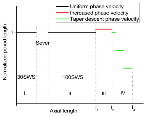
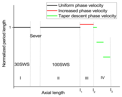
The optimal periodic tapering combination identified is RSM + GA(200). Figure 10 illustrates the resulting phase velocity profile of the slow-wave structure (SWS) along the entire tube. The period of the tapered structure initially increases and then decreases, causing the phase velocity of the slow wave to follow a similar pattern. This tapering configuration corresponds closely with the electron energy distribution shown in Figure 9. At the output end of the DCWWG traveling-wave tube, many electrons are accelerated to energy levels that make interaction with a uniform SWS challenging; therefore, the phase velocity of the SWS must be increased to maintain effective interaction with these electrons. Conversely, a significant number of electrons lose energy and cluster around 7.5 kV, necessitating interaction with an SWS section that has a lower phase velocity.
Figure 10.
Design scheme of phase-tapered TWT.
4.3. PIC Simulation Verification
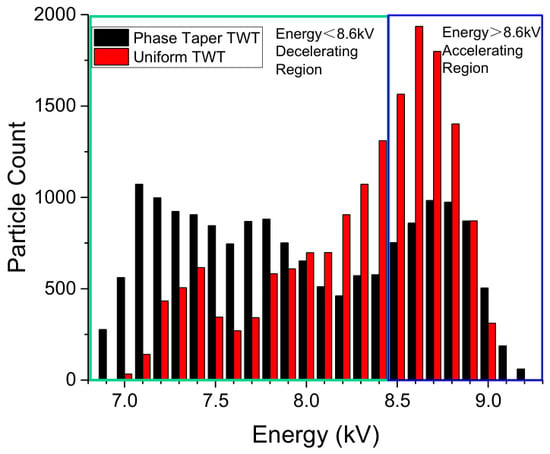
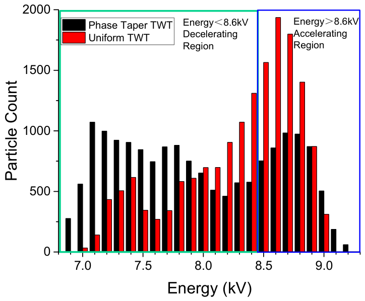
Figure 11 shows the electron energy distribution analysis results of the last 10 cycles of DCWWG TWT and phase-tapered TWT under the conditions of input power of 0.125 W and center frequency f0 = 220 GHz.
Figure 11.
Energy distribution of electrons in the last 10 periods of two TWTs.
At the end of the TWT, a large amount of electron energy in the DCWWG-based uniform TWT remains concentrated around 8.6 kV and is not fully utilized. The electron energy of the Taper TWT decreases significantly, which means that the interaction efficiency of the Taper TWT is significantly stronger than that of the uniform TWT.
Figure 12 illustrates the electron clustering state at the end of the stabilized TWT. The introduction of the phase taper structure disrupts the previously saturated electron clustering equilibrium, causing the electrons to interact once again with the slow wave, which has a low phase velocity. As shown, the phase taper SWS used at the end of the TWT reduces the phase velocity, thereby improving the interaction efficiency of the electrons and further enhancing the TWT’s output power.
Figure 12.
Electron clustering state at the end of the stabilized TWT.
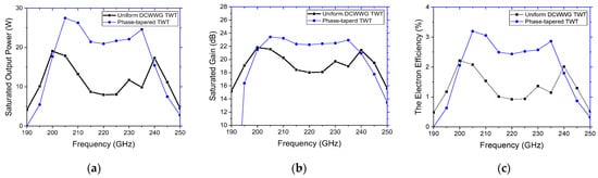
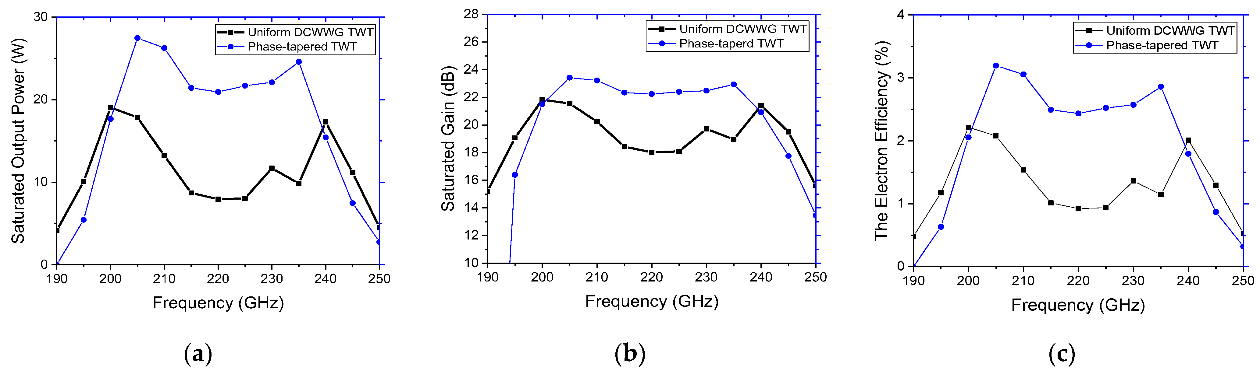
Figure 13 compares the output power and efficiency of a uniform DCWWG TWT with those of a DCWWG TWT featuring phase velocity tapering, both operating under identical parameters. Across the 205–235 GHz frequency range, the tapered DCWWG TWT exhibits significantly higher saturated output power, electronic efficiency, and gain compared to the standard DCWWG TWT; however, its half-power bandwidth is slightly narrower. At the center frequency of 220 GHz, the standard DCWWG TWT produces an output power of approximately 8 W, while the phase-velocity-stepped DCWWG TWT delivers about 22.1 W. The standard DCWWG TWT reaches a maximum output power of around 19 W at 200 GHz with an efficiency of 2.2%, whereas the phase-velocity-stepped DCWWG TWT achieves a maximum output power of approximately 28 W at 205 GHz with an efficiency of 3.2%. This corresponds to an increase in maximum output power of roughly 47%. These findings clearly demonstrate that phase velocity stepping technology significantly improves the output performance of DCWWG TWTs.
Figure 13.
Performance comparison of a uniform DCWWG TWT and a phase-tapered TWT: (a) saturated output power; (b) saturated amplification gain; (c) saturated operating efficiency.
5. Conclusions
This paper explores the use of a double-corrugated waveguide with a wide grating slow-wave structure (DCWWG SWS), which features high interaction impedance and low phase velocity within its operating range, to design a low-voltage terahertz traveling-wave tube (TWT). The output power of the TWT is enhanced through the application of periodic-hopping technology. Our investigation into the fundamental properties of this slow-wave structure revealed that incorporating a wide slot significantly reduces phase velocity while increasing interaction impedance. Based on these findings, we designed a low-voltage two-stage TWT capable of interacting with an 8.6 kV cylindrical electron beam. To further boost the TWT’s output power, we introduced a phase-tapering technique. Using response surface methodology, we developed a second-order polynomial model incorporating power, which provided an initial phase taper scheme. This scheme was then optimized using a genetic algorithm to produce the final periodically hopping TWT design. Particle-in-cell (PIC) simulations demonstrated that, across the 205–235 GHz frequency range, the saturated output power and gain of the phase-tapered TWT significantly exceed those of a uniform TWT. The designed phase-tapered TWT delivers a maximum output power of approximately 28 W, which is about 47% higher than the 19 W maximum output power of a conventional wide-slot double-corrugated waveguide TWT. Additionally, it achieves a bandwidth of approximately 15% at 3 dB. These results demonstrate that phase-tapering technology markedly enhances the output performance of the DCWWG TWT. Consequently, the wide-slot-based double-corrugated waveguide slow-wave structure offers an effective solution for high-power terahertz radiation sources.
Author Contributions
Conceptualization, W.W. and Z.Z.; methodology, Z.Q. and F.Z.; software, F.Z.; validation, Z.Q., F.Z. and Z.Z.; formal analysis, W.W.; investigation, Z.Q.; resources, F.Z.; data curation, W.W.; writing—original draft preparation, W.W.; writing—review and editing, Z.Q. and W.L.; visualization, W.W.; supervision, Z.Z.; project administration, F.Z.; funding acquisition, F.Z. and Z.Q. All authors have read and agreed to the published version of the manuscript.
Funding
This work was supported in part by the National Key Research and Development Program of China under Grant 2023YFF0719402 and the National Natural Science Foundation of China under Grant U22A2020 and Science Foundation of the Aerospace Information Research Institute under Grant E2Z213010F.
Data Availability Statement
The original contributions presented in this study are included in the article. Further inquiries can be directed to the corresponding author.
Conflicts of Interest
The authors declare that they have no conflicts of interest.
References
- Paoloni, C.; Gamzina, D.; Letizia, R.; Zheng, Y.; Luhmann, N.C., Jr. Millimeter Wave Traveling Wave Tubes for the 21st Century. J. Electromagn. Waves Appl. 2021, 35, 567–603. [Google Scholar] [CrossRef] [Scilit]
- Anilkumar, P.; Wang, S.; Gong, Y. Challenges in the Design and Development of Slow-Wave Structure for THz Traveling-Wave Tube: A Tutorial Review. Electronics 2025, 14, 2624. [Google Scholar] [CrossRef] [Scilit]
- Wang, S.; Gong, Y.; Wang, Z.; Wei, Y.; Duan, Z.; Feng, J.; Liu, Q. Study of Low-Voltage Radial Convergent Sheet Electron Optical System. IEEE Trans. Plasma Sci. 2014, 42, 1847–1853. [Google Scholar] [CrossRef] [Scilit]
- Bian, X.; Pan, P.; Du, X.; Feng, Y.; Li, Y.; Song, B.; Feng, J. Design and Experiment of Modified Folded Waveguide Slow Wave Structure for 60-W G-Band Traveling Wave Tube. IEEE Microw. Wirel. Technol. Lett. 2025, 35, 1194–1197. [Google Scholar] [CrossRef] [Scilit]
- Nayek, N.; Sonkar, R.; Joshi, M.K.; Tiwari, T.; Bhattacharjee, R. H-Plane Loaded Sine Waveguide TWT in G-Band. In Proceedings of the 2019 IEEE Asia-Pacific Microwave Conference (APMC); IEEE: Piscataway, NJ, USA, 2019; pp. 1250–1252. [Google Scholar]
- Zhao, C.; Xu, H. A Modified Double Staggered Grating Waveguide Slow Wave Structure for Sub-THz Traveling Wave Tubes. IEEE Trans. Electron Devices 2023, 70, 2746–2752. [Google Scholar] [CrossRef] [Scilit]
- Liu, S. Suppressing Arcing Phenomenon for MW/MMW CCTWT. Int. J. Infrared Millim. Waves 2004, 25, 1061–1067. [Google Scholar] [CrossRef] [Scilit]
- Bhattacharjee, S.; Booske, J.H.; Kory, C.L.; Van Der Weide, D.W.; Limbach, S.; Gallagher, S.; Welter, J.D.; Lopez, M.R.; Gilgenbach, R.M.; Ives, R.L.; et al. Folded Waveguide Traveling-Wave Tube Sources for Terahertz Radiation. IEEE Trans. Plasma Sci. 2004, 32, 1002–1014. [Google Scholar] [CrossRef] [Scilit]
- Sarkar, M.; Kumar, N. Pseudospark Discharge-Based Electron Beam Sources: A Review. IEEE Trans. Plasma Sci. 2024, 52, 1966–1982. [Google Scholar] [CrossRef] [Scilit]
- Gamzina, D.; Himes, L.G.; Barchfeld, R.; Zheng, Y.; Popovic, B.K.; Paoloni, C.; Choi, E.; Luhmann, N.C. Nano-CNC Machining of Sub-THz Vacuum Electron Devices. IEEE Trans. Electron Devices 2016, 63, 4067–4073. [Google Scholar] [CrossRef] [Scilit]
- Gamzina, D.; Li, H.; Himes, L.; Barchfeld, R.; Popovic, B.; Pan, P.; Letizia, R.; Mineo, M.; Feng, J.; Paoloni, C.; et al. Nanoscale Surface Roughness Effects on THz Vacuum Electron Device Performance. IEEE Trans. Nanotechnol. 2016, 15, 85–93. [Google Scholar] [CrossRef] [Scilit]
- Minenna, D.F.G.; André, F.; Elskens, Y.; Auboin, J.-F.; Doveil, F.; Puech, J.; Duverdier, É. The Traveling-Wave Tube in the History of Telecommunication. Eur. Phys. J. H 2019, 44, 1–36. [Google Scholar] [CrossRef] [Scilit]
- Basu, R.; Rao, J.M.; Le, T.; Letizia, R.; Paoloni, C. Development of a D-Band Traveling Wave Tube for High Data-Rate Wireless Links. IEEE Trans. Electron Devices 2021, 68, 4675–4680. [Google Scholar] [CrossRef] [Scilit]
- Li, X.; Huang, X.; Mathisen, S.; Letizia, R.; Paoloni, C. Design of 71–76 GHz Double-Corrugated Waveguide Traveling-Wave Tube for Satellite Downlink. IEEE Trans. Electron Devices 2018, 65, 2195–2200. [Google Scholar] [CrossRef] [Scilit]
- Paoloni, C.; Mineo, M.; Henry, M.; Huggard, P.G. Double Corrugated Waveguide for Ka-Band Traveling Wave Tube. IEEE Trans. Electron Devices 2015, 62, 3851–3856. [Google Scholar] [CrossRef] [Scilit]
- Wang, W.; Qu, Z.; Liu, W.; Zhu, F.; Zhang, Z.; Xue, Q. Double-Corrugated Waveguide Slow Wave Structure with Grating for THz Backward Wave Oscillator. IEEE Trans. Plasma Sci. 2025, 53, 1660–1665. [Google Scholar] [CrossRef] [Scilit]
- Wang, S.; Chung, K.L.; Du, L.; Kong, F.; Li, K. Design and Analysis of a Compact Frequency Beam-Scanning Antenna Based on Composite FHMSIW/SSPP Waveguide. IEEE Antennas Wirel. Propag. Lett. 2021, 21, 546–550. [Google Scholar] [CrossRef] [Scilit]
- Mineo, M.; Di Carlo, A.; Paoloni, C. Analytical Design Method for Corrugated Rectangular Waveguide SWS THz Vacuum Tubes. J. Electromagn. Waves Appl. 2010, 24, 2479–2494. [Google Scholar] [CrossRef] [Scilit]
- Yi, H.; Xiao, L.; Liu, P.; Li, F. Optimization Design of Slow Wave Structure Using Genetic Algorithm. In Proceedings of the 2011 IEEE International Vacuum Electronics Conference (IVEC); IEEE: Piscataway, NJ, USA, 2011; pp. 215–216. [Google Scholar]

Disclaimer/Publisher’s Note: The statements, opinions and data contained in all publications are solely those of the individual author(s) and contributor(s) and not of MDPI and/or the editor(s). MDPI and/or the editor(s) disclaim responsibility for any injury to people or property resulting from any ideas, methods, instructions or products referred to in the content. |
© 2026 by the authors. Licensee MDPI, Basel, Switzerland. This article is an open access article distributed under the terms and conditions of the Creative Commons Attribution (CC BY) license.