


Abstract
This work demonstrates the potential of indium germanium zinc oxide (InGeZnO) as a promising oxide semiconductor offering an improved trade-off between mobility and stability under water exposure and thermal stress. The effect of Ge incorporation in enhancing the stability of indium zinc oxide (InZnO) thin-film transistors (TFTs) is systematically investigated through negative bias stress (NBS) and negative bias temperature stress (NBTS) measurements after different durations of deionized-water immersion. The results show that InGeZnO exhibits smaller threshold voltage () shift magnitudes and reduced subthreshold swing (SS) degradation after prolonged immersion, as well as an attenuated difference between the SS changes induced by NBS and NBTS, compared with InZnO. These electrical trends suggest that water exposure disrupts the metal–oxygen (M–O) coordination structure and increases oxygen vacancies in the exposed back channel, whereas Ge–O bonding stabilizes the M–O network and limits the evolution of these defects under gate bias and thermal stress. X-ray photoelectron spectroscopy (XPS) analysis provides further support for the proposed mechanism. Collectively, the results position Ge doping as a promising strategy for balancing high mobility with robust stability against water vapor exposure and thermal stress in oxide TFTs.
1. Introduction
High-performance thin film transistors (TFTs) are essential switching devices in active matrix displays to enable high resolution and frame rate operation. Metal oxide (MO) TFTs, which benefit from relatively high field-effect mobility () and good process compatibility, have been widely regarded as promising candidates for next-generation display driving technologies [1,2,3,4] and capacitorless memory applications [5]. In particular, indium gallium zinc oxide (InGaZnO) has been extensively adopted in practical applications owing to its mature material system and established fabrication processes [6,7]. However, its field-effect mobility () typically remains around 10 to 15 cm2 V−1 s−1 [8,9,10], which limits the performance margin for displays with higher frame rates and pixel densities. Meanwhile, other MO TFTs with higher mobility, such as InZnO [11,12,13] and IZTO [14,15,16], often exhibit greater electrical instability, reflecting the trade-off between mobility and reliability [17,18]. In this regard, Ge incorporation into InZnO has attracted increasing attention [19,20,21,22]. The high dissociation energy of Ge–O bonds stabilizes the local coordination structure [22,23,24,25], increasing the formation energy of oxygen vacancies (), thereby improving electrical stability. In addition, Ge doping has been reported to reduce carrier localization, which is commonly attributed to the more delocalized nature of Ge 4s orbitals near the conduction band edge [24], maintaining relatively high at low dopant concentrations. Consequently, indium germanium zinc oxide (InGeZnO) has been considered a promising channel material for achieving stable TFTs with high .
Nevertheless, the reliability of InGeZnO TFTs under different stress conditions remains to be further clarified. Extensive reliability investigations have been reported under illumination [26,27], thermal stress [28,29,30,31], and electrical bias stress [32,33,34,35]. Previous studies have mitigated moisture-related instability through channel densification and back-channel passivation [15,36,37,38,39]. However, studies concerning the effects of direct water exposure on the reliability of Ge-containing oxide TFTs are still limited. In this work, the stability of InGeZnO TFTs following prolonged water exposure is systematically investigated, with InZnO serving as the reference. To minimize interference from other ambient species, both types of TFTs were directly immersed in deionized water at room temperature (RT) for various durations up to 8 h. After each immersion period, NBS and NBTS measurements were performed under the same negative gate bias at RT and 55 °C, respectively, to quantify the accelerating effect of elevated temperature on the evolution of water-induced defects in the back channel. The resulting degradation was assessed using the shift magnitude and SS change. As the immersion duration increased from 0 to 8 h, the differences between NBS and NBTS in these two parameters increased by only 0.15 V and 148.03 mV/dec, respectively, for InGeZnO, whereas the corresponding increases for InZnO were 0.64 V and 360.69 mV/dec. These results demonstrate the improved resistance of InGeZnO to water-related degradation under NBS and its further enhancement under thermal stress. Furthermore, a degradation mechanism was proposed and supported by X-ray photoelectron spectroscopy (XPS) analysis: water immersion disrupts M–O coordination in the back channel and induces oxygen-related defects; Ge–O bonds enhance structural stability owing to their high bond dissociation energy, reducing the reactivity of oxygen-deficient regions toward water and suppressing further defect formation and electrical activation under subsequent electrical and thermal stresses.
2. Experimental Section
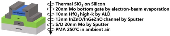
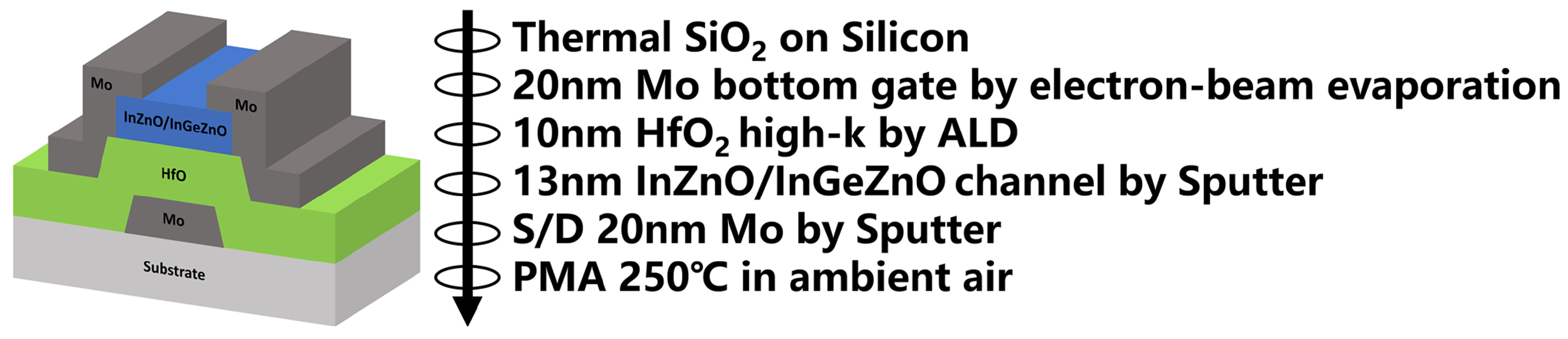
Bottom-gate, top-contact InZnO and InGeZnO TFTs were fabricated on p-type Si substrates with a 90 nm thick thermally grown SiO2 layer. A 20 nm Mo gate electrode was first deposited by electron-beam evaporation and patterned. A 10 nm HfO2 gate dielectric was then deposited by atomic layer deposition at 300 °C. Subsequently, the InZnO and InGeZnO active layers were prepared by magnetron sputtering at room temperature under a working pressure of 3 mTorr. The InZnO layers were deposited by radio-frequency sputtering at 80 W under Ar and O2 flow rates of 28 and 2 sccm, respectively. For the InGeZnO channel, ultrathin Ge layers were periodically inserted into the InZnO deposition sequence by direct-current sputtering at 10 W under an Ar flow rate of 20.5 sccm. The sputtering duration of each Ge insertion was fixed at 8 s, producing an InZnO/Ge/InZnO/Ge/InZnO stacked structure, as illustrated in Figure 1. For comparison, the InZnO channel was fabricated under the same deposition conditions without Ge insertion. The total channel thickness was approximately 13 nm. Afterwards, a 20 nm thick Mo layer was deposited by magnetron sputtering and patterned through a lift-off process to form the source/drain electrodes. Finally, all fabricated devices were annealed in ambient air at 250 °C for 30 min.
Figure 1.
The schematic diagram of the TFT device and the detailed process flow.
Electrical characterization was performed on TFTs with a channel width of 80 m and channel lengths of 30, 20, and 10 m (, , and m/m). To account for differences in channel dimensions, the drain current was normalized as , and all drain current values presented in the subsequent figures and discussion refer to . Transfer characteristics were measured in ambient air by sweeping from to 3 V at V. The was extracted using the constant-current method and defined as the gate voltage at which reached 10 nA. The SS was calculated from , with its average over the range from to A reported. The was calculated in the linear region using , where and is the gate dielectric capacitance per unit area. The maximum within the measured range was reported. NBS and NBTS measurements were conducted at V for 1000 s at RT and 55 °C, respectively, unless stated otherwise. Each reported data point represents the mean ± standard deviation obtained from 10 TFTs measured under the corresponding test condition.
3. Results and Discussion
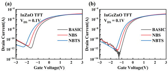
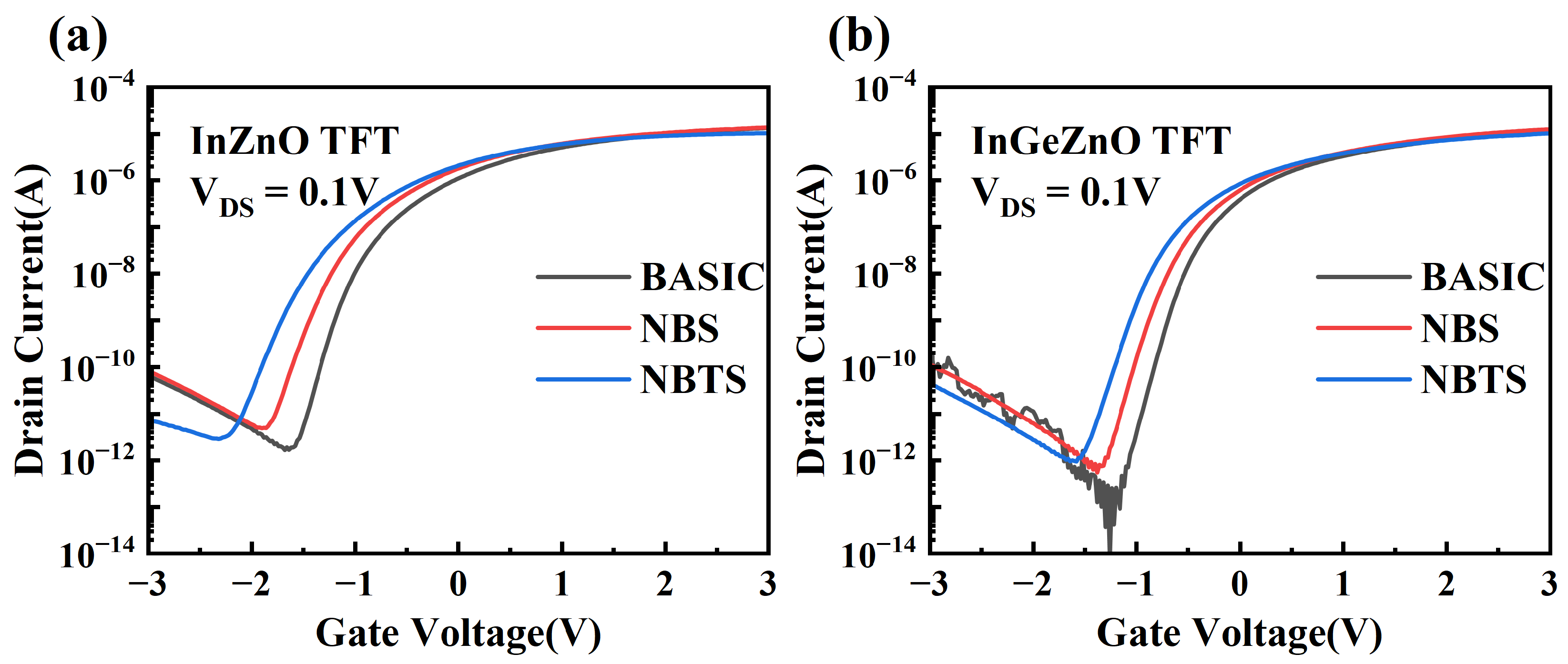
Figure 2 illustrates the transfer characteristics of InZnO [Figure 2a] and InGeZnO [Figure 2b] TFTs in the initial state, after NBS and NBTS, prior to water immersion. Table 1 summarizes the mean initial parameters obtained from multiple devices, showing that InGeZnO exhibits a more positive ( versus V) and a smaller SS (111.44 versus 145.90 mV/dec) without sacrificing (41.35 versus 40.63 cm2 V−1 s−1). The observed differences in and SS are attributed to Ge–O bonding, which enhances lattice stability and raises the formation energy of [22,23,24,25]. Meanwhile, Ge incorporation enhances the spatial overlap of In 5s orbitals, increasing conduction-band dispersion and lowering the conduction-band minimum (CBM), thereby reducing the donor activation energy. The increased dispersion enables InGeZnO to maintain a comparable to that of InZnO, while the lower activation energy allows a larger fraction of the remaining donor-derived electrons to be activated into the conduction band despite the reduced concentration of donors [17,24,40]. Furthermore, comparison of the pre-immersion stress responses reveals better stability in InGeZnO than in InZnO under both NBS and NBTS. Driven by the negative gate electric field, ionized migrate toward the gate–insulator interface, and the resulting interfacial accumulation promotes charge trapping, leading to the negative shift and SS degradation. Elevated temperature further promotes the ionization of deep-level defects in the back channel and increases the electron concentration, resulting in more severe electrical degradation under NBTS.
Figure 2.
Transfer curves of (a) InZnO and (b) InGeZnO TFTs in the initial state and after NBS and NBTS measured at V.
Table 1.
Initial electrical parameters of the InZnO and InGeZnO TFTs. Values are presented as the mean ± standard deviation obtained from 10 devices for each condition ().
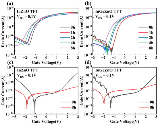
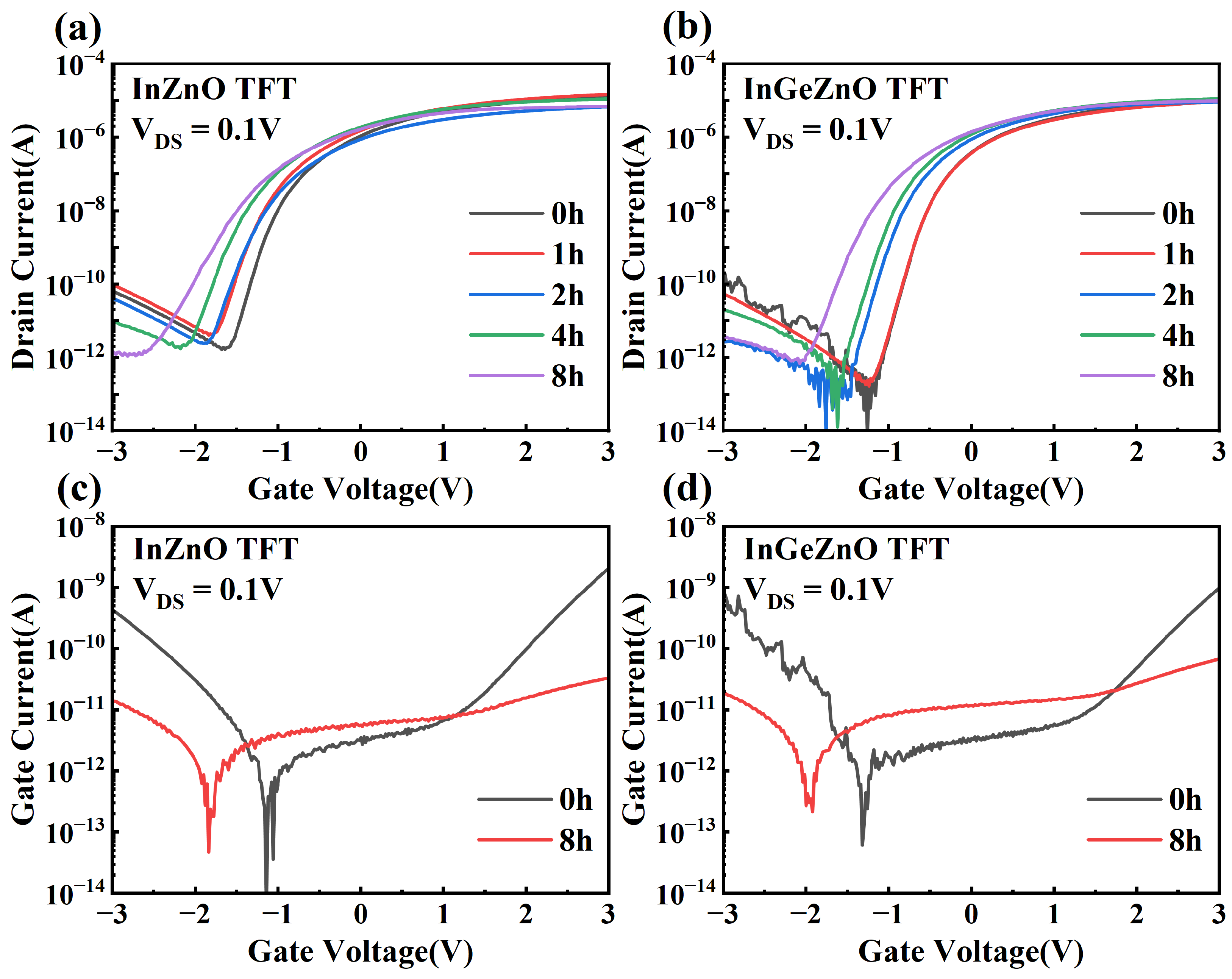
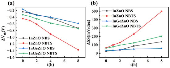
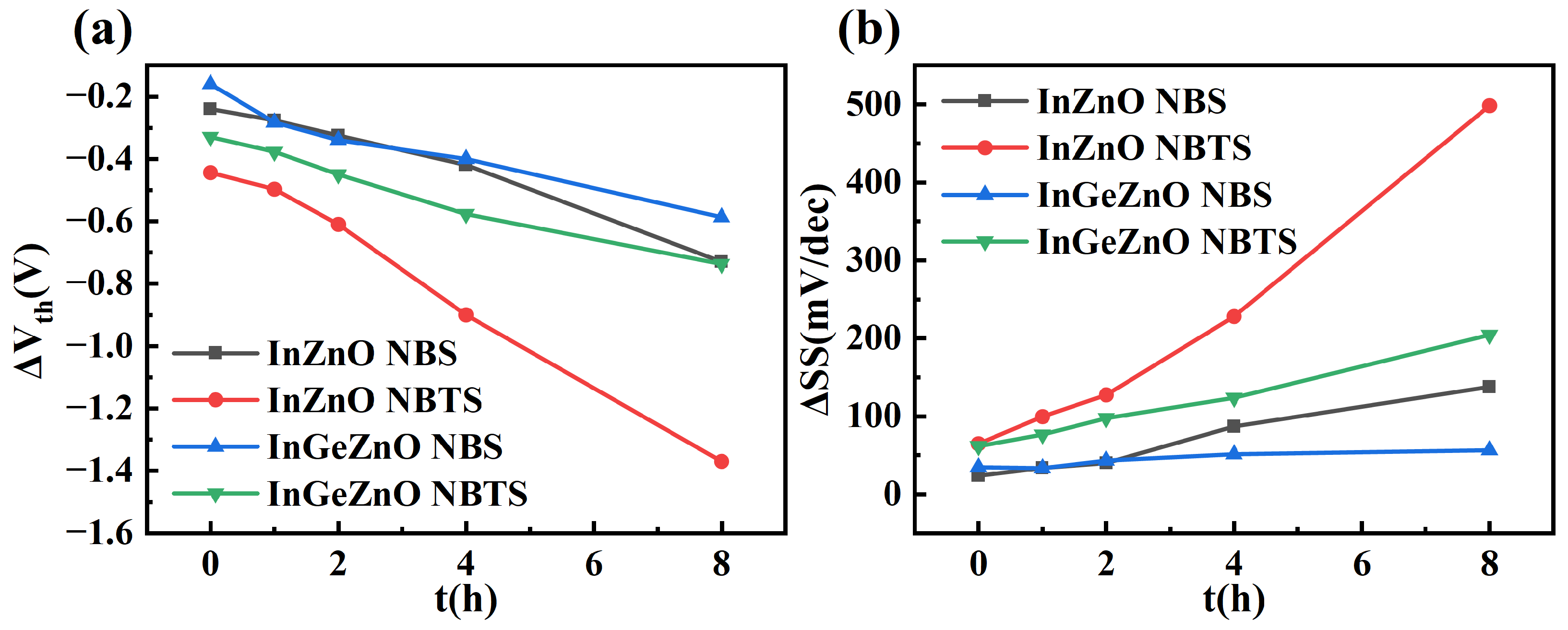
Figure 3 presents the transfer characteristics of InZnO [Figure 3a] and InGeZnO [Figure 3b] TFTs after different durations of deionized-water immersion. The curves exhibit an overall negative shift and increased off-current with increasing immersion time, indicating an increase in the channel electron concentration. Notably, the switching characteristics of InZnO deteriorate markedly by 8 h, suggesting appreciable modification of the channel. Figure 3c,d show no evident increase in gate leakage for either TFT after 8 h of immersion, suggesting that gate-stack degradation is unlikely to dominate the observed transfer-characteristic changes. In order to comprehensively evaluate the effects of water exposure and elevated temperature on the channel, InZnO and InGeZnO TFTs were examined under NBS and NBTS after different durations of immersion. The shift magnitudes () and SS changes () extracted from the transfer characteristics measured before and after stress are summarized in Figure 4a for InZnO and Figure 4b for InGeZnO. The extracted data indicate that both and generally increase with immersion duration under NBS; more importantly, NBTS produces substantially larger values of both quantities. To quantify the additional electrical degradation associated with elevated temperature, and are defined as the differences between the NBTS- and NBS-induced and values, respectively, at the same immersion duration :
Figure 3.
Transfer characteristics of (a) InZnO and (b) InGeZnO TFTs before and after immersion in deionized water for 1, 2, 4, and 8 h; gate leakage current characteristics of (c) InZnO and (d) InGeZnO TFTs before and after 8 h of immersion.
Figure 4.
Dependence of (a) and (b) on the duration of immersion in deionized water for InZnO and InGeZnO TFTs subjected to NBS and NBTS.
As summarized in Table 2, from 0 to 8 h, and in InZnO increase from 0.20 to 0.64 V and from 41.06 to 360.69 mV/dec, whereas the corresponding values in InGeZnO change from 0.17 to 0.15 V and from 26.90 to 148.03 mV/dec. Previous studies on the effects of water on oxide TFTs have mainly explained shifts in terms of surface adsorption: adsorbed water molecules can induce an additional electron accumulation layer at the channel surface, thereby increasing the electron concentration and resulting in a negative shift [40,41,42]. The increased shift observed in this work is consistent with this model. However, it mainly accounts for the change in carrier concentration caused by water adsorption and does not fully explain the pronounced increase in after immersion relative to the 0 h baseline. It is therefore reasonable to speculate that water exposure also perturbs the local M–O coordination environment and increases the electrical activity of defects in the channel, with Ge incorporation suppressing such changes.
Table 2.
Thermal contributions to the shift () and SS degradation () in InZnO and InGeZnO TFTs before and after 1, 2, 4, and 8 h of immersion in deionized water.
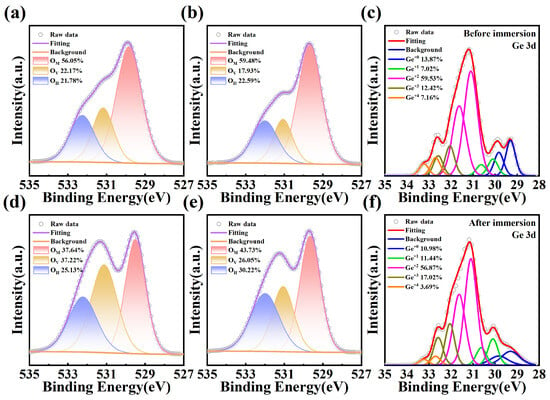
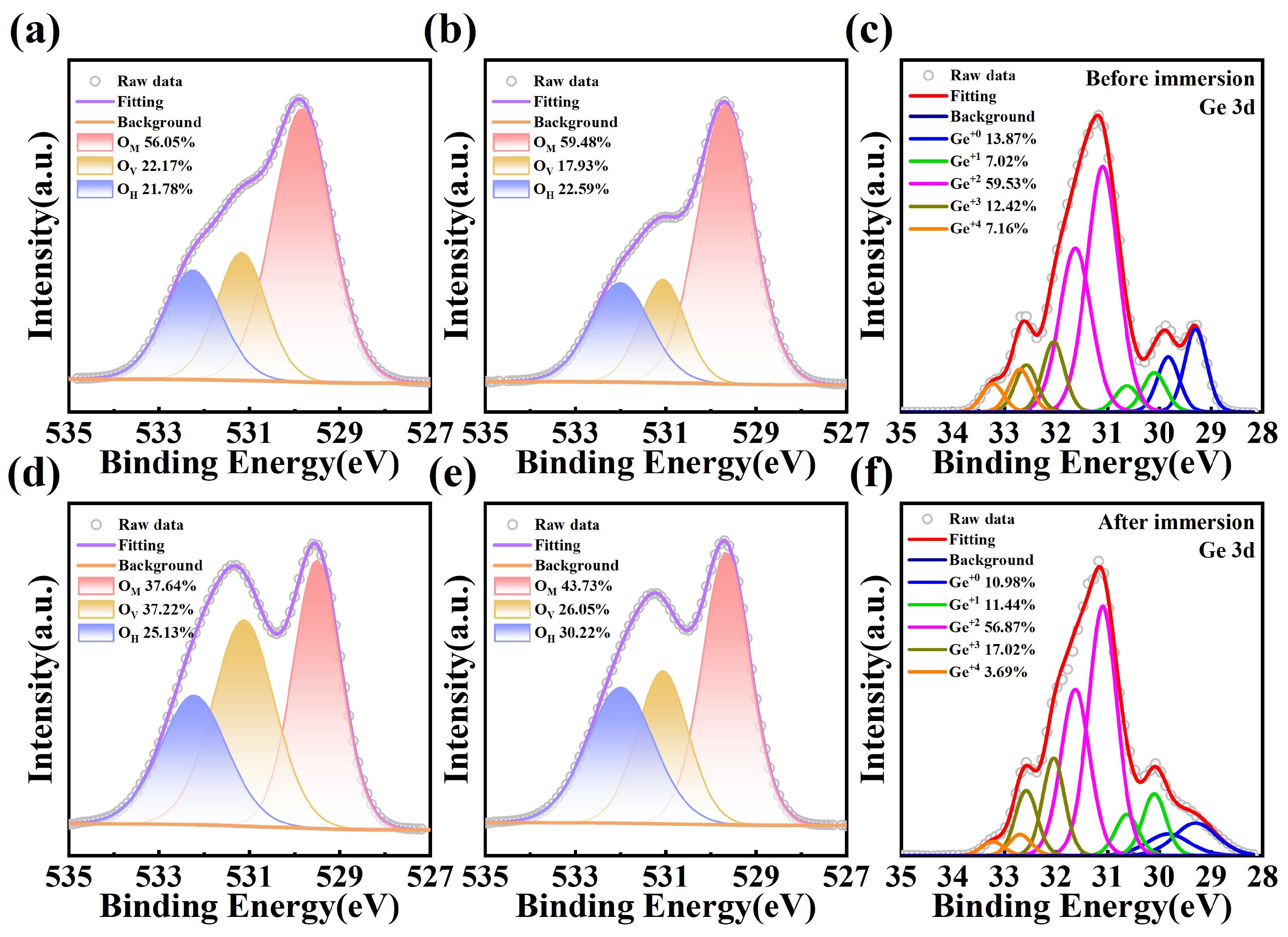
In terms of material properties, XPS was employed to investigate the influence of water exposure on the chemical states of InZnO and InGeZnO films. Generally, the O 1s spectra can be deconvoluted into three subpeaks with binding energy centered at 529.7 ± 0.1 eV (peak 1), 531.1 ± 0.1 eV (peak 2), and 531.9 ± 0.1 eV (peak 3), respectively, representing metal-bonding oxygens, oxygen associated with oxygen vacancies (), and chemisorbed oxygens [43,44,45]. Figure 5a–c show the InZnO O 1s and InGeZnO O 1s and Ge 3d spectra before immersion, whereas Figure 5d–f show the corresponding spectra after 8 h of immersion in deionized water. Relative to the initial state, the composition of peak 1 decreases by 18.41 percentage points in InZnO, compared with 15.75 percentage points in InGeZnO; a more pronounced contrast is observed for peak 2, with its composition increasing by 15.05 percentage points in InZnO but by only 8.12 percentage points in InGeZnO. The changes observed in InZnO are consistent with the selective etching mechanism previously proposed for IGZO after deionized water immersion [40]. According to this mechanism, water preferentially reacts with Ga and Zn sites near , disrupting the M–O network and increasing the relative fractions of In and at the exposed surface. By contrast, Figure 5c,f show only limited redistribution among the fitted Ge 3d components, with the average Ge oxidation state remaining nearly unchanged after immersion. Together with the smaller O 1s changes in InGeZnO, this result suggests that Ge-related local coordination is largely preserved during water immersion, consistent with the stabilizing role of Ge–O bonding in the local M–O network.
Figure 5.
O 1s XPS spectra of the InZnO and InGeZnO films and Ge 3d XPS spectra of the InGeZnO film measured before immersion (a–c) and after 8 h of immersion in deionized water (d–f): (a,d) InZnO O 1s; (b,e) InGeZnO O 1s; and (c,f) InGeZnO Ge 3d.
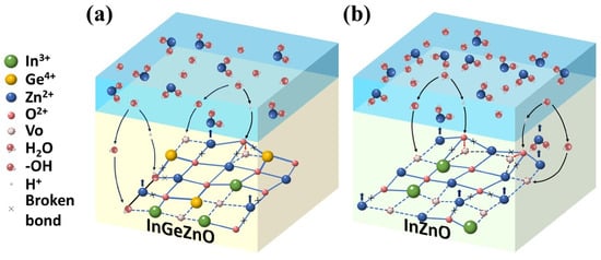
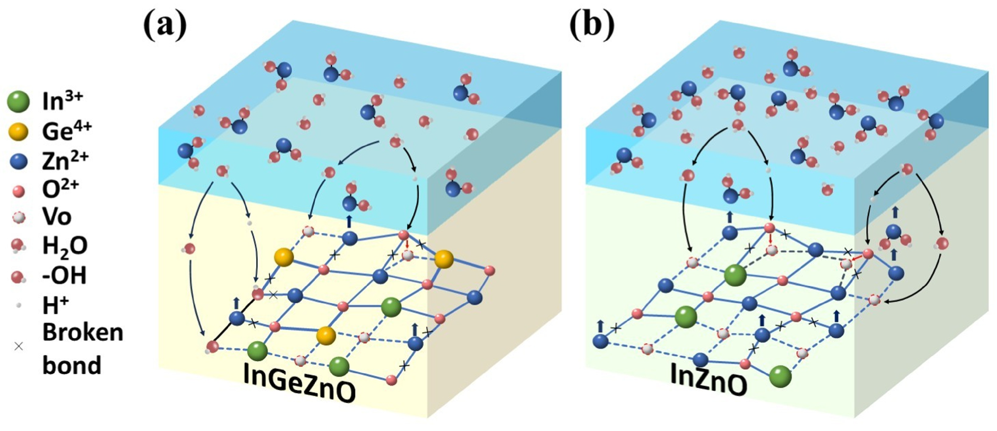
Based on the combined XPS and electrical results, a mechanism is proposed, as schematically illustrated in Figure 6. The process can be divided into two stages: water immersion and subsequent bias stress. During immersion, oxygen-deficient regions at the exposed back-channel surface are particularly vulnerable to water, which may preferentially disrupt nearby Zn–O bonds [40]. The preferential loss of Zn species further weakens the surrounding M–O network, resulting in In enrichment and an increased concentration of at the exposed surface, as supported by the pronounced decrease in peak 1 and the marked increase in peak 2 observed in the O 1s spectra of InZnO after immersion. Under the gate electric field, defects in the back channel exert a greater influence on device characteristics. Thermal stress may further accelerate structural rearrangement, promoting the formation and electrical activation of . This process can be well reflected in a marked increase in channel conductivity and more pronounced SS degradation in InZnO. By contrast, Ge incorporation markedly suppresses this degradation process. The high bond dissociation energy of Ge–O bonds strengthens the structure and reduces the reactivity of oxygen-deficient regions. This greater resistance curbs further structural degradation and limits the generation of additional . XPS analysis clearly demonstrates the effect, with peak 2 showing a smaller difference in InGeZnO after immersion. This stabilization also persists under NBTS, restricting the generation and electrical activation of donor-like defects and trap states. As a result, thermal stress produces less additional degradation in InGeZnO, leading to smaller negative shifts and milder SS degradation.
Figure 6.
Schematic diagrams of the proposed degradation mechanism at the exposed back channel of (a) InGeZnO and (b) InZnO during water exposure.
4. Conclusions
In this study, Ge incorporation was investigated as a material strategy to improve the stability of InZnO TFTs under water exposure and thermal stress. The resulting InGeZnO TFTs maintained a of 41.35 cm2 V−1 s−1 and an initial of −0.53 V with enhanced stability. After 8 h of deionized water immersion, the NBTS-induced shift magnitude and SS increase are limited to 0.74 V and 204.33 mV/dec, respectively. Utilizing NBS and NBTS measurements together with O 1s and Ge 3d XPS analyses, we elucidated the mechanism of back-channel degradation induced by water exposure and further promoted by thermal stress. The results further demonstrate the role of Ge–O bonding in stabilizing the M–O network and effectively suppressing this degradation. Therefore, InGeZnO TFTs may be promising candidates for next-generation displays designed to operate in extreme environments with high temperature and humidity.
Author Contributions
Conceptualization, Y.Y. and D.R.; methodology, Y.Y.; formal analysis, Y.Y.; investigation, Y.Y. and S.P.; resources, S.P., J.X. and D.R.; data curation, Y.Y. and W.L.; writing—original draft preparation, Y.Y.; writing—review and editing, Y.Y. and J.X.; visualization, W.L.; supervision, D.R. and S.W.; project administration, D.R. and S.W.; funding acquisition, D.R. All authors have read and agreed to the published version of the manuscript.
Funding
This work was supported in part by the National Natural Science Foundation of China under Grant 62574046, Grant 92464206, Grant 62474044 and Grant 62204043; in part by the National Science Fund for Distinguished Young Scholars of Fujian Province under Grant 2026J010017; in part by the MIND project under Grant MINDKT202405 and Grant MINDKT202501; in part by open project SKSP202508 of the State Key Laboratory of Semiconductor Physics and Chip Technologies; and in part by the Fujian College Association Instrumental Analysis Center of Fuzhou University Testing Fund of Precious Apparatus 2026T067, 2026T068, and 2026T070. The APC was funded by the authors.
Data Availability Statement
The original contributions presented in this study are included in the article. Further inquiries can be directed to the corresponding authors.
Conflicts of Interest
The authors declare no conflicts of interest. The funders had no role in the design of the study; in the collection, analyses, or interpretation of data; in the writing of the manuscript; or in the decision to publish the results.
References
- Zhang, L.; Yu, H.; Xiao, W.; Liu, C.; Chen, J.; Guo, M.; Gao, H.; Liu, B.; Wu, W. Strategies for applications of oxide-based thin film transistors. Electronics 2022, 11, 960. [Google Scholar] [CrossRef] [Scilit]
- Lee, S.-H.; Bak, S.-Y.; Yi, M. Improved performance and bias stability of Al2O3/IZO thin-film transistors with vertical diffusion. Electronics 2022, 11, 2263. [Google Scholar] [CrossRef] [Scilit]
- Jeong, H.-S.; Cha, H.-S.; Hwang, S.-H.; Kwon, H.-I. Effects of annealing atmosphere on electrical performance and stability of high-mobility indium-gallium-tin oxide thin-film transistors. Electronics 2020, 9, 1875. [Google Scholar] [CrossRef] [Scilit]
- Kamiya, T.; Hosono, H. Material characteristics and applications of transparent amorphous oxide semiconductors. NPG Asia Mater. 2010, 2, 15–22. [Google Scholar] [CrossRef] [Scilit]
- Xiang, J.; Ruan, D.-B.; Tang, Z.; Zhang, Z.B.; Wang, S.H.; Lin, Z.T.; Yang, Y.C.; Li, T.; Zhao, Z.; Gan, K.-J.; et al. Amorphous oxide semiconductor thin-film transistor using different source–drain electrode metals and its application in 2T0C memory arrays. IEEE Trans. Electron. Devices 2026, 73, 360–366. [Google Scholar] [CrossRef] [Scilit]
- Lee, J.S.; Chang, S.; Koo, S.-M.; Lee, S.Y. High-performance a-IGZO TFT with ZrO2 gate dielectric fabricated at room temperature. IEEE Electron. Device Lett. 2010, 31, 225–227. [Google Scholar] [CrossRef] [Scilit]
- Yu, M.-C.; Ruan, D.-B.; Liu, P.-T.; Chien, T.-C.; Chiu, Y.-C.; Gan, K.-J.; Sze, S.M. High performance transparent a-IGZO thin film transistors with ALD-HfO2 gate insulator on colorless polyimide substrate. IEEE Trans. Nanotechnol. 2020, 19, 481–485. [Google Scholar] [CrossRef] [Scilit]
- Yao, J.; Xu, N.; Deng, S.; Chen, J.; She, J.; Shieh, H.-P.D.; Liu, P.-T.; Huang, Y.-P. Electrical and photosensitive characteristics of a-IGZO TFTs related to oxygen vacancy. IEEE Trans. Electron. Devices 2011, 58, 1121–1126. [Google Scholar] [CrossRef] [Scilit]
- Chen, R.; Zhou, W.; Zhang, M.; Wong, M.; Kwok, H.S. Self-aligned indium-gallium-zinc oxide thin-film transistor with source/drain regions doped by implanted arsenic. IEEE Electron. Device Lett. 2013, 34, 60–62. [Google Scholar] [CrossRef] [Scilit]
- Xu, X.; Zhang, M.; Yang, Y.; Lu, L.; Lin, F.; Wong, M.; Kwok, H.-S. Realization of visible-light detection in InGaZnO thin-film transistor via oxygen vacancy modulation through N2 treatments. Adv. Electron. Mater. 2023, 9, 2300351. [Google Scholar] [CrossRef] [Scilit]
- Morales-Masis, M.; De Nicolas, S.M.; Holovsky, J.; De Wolf, S.; Ballif, C. Low-temperature high-mobility amorphous IZO for silicon heterojunction solar cells. IEEE J. Photovolt. 2015, 5, 1340–1347. [Google Scholar] [CrossRef] [Scilit]
- Song, J.-I.; Park, J.-S.; Kim, H.; Heo, Y.-W.; Lee, J.-H.; Kim, J.-J.; Kim, G.M.; Choi, B.D. Transparent amorphous indium zinc oxide thin-film transistors fabricated at room temperature. Appl. Phys. Lett. 2007, 90, 022106. [Google Scholar] [CrossRef] [Scilit]
- Lai, K.; Liu, Y.; Li, M.; Wang, D.; Li, Y.; Yao, R.; Geng, K.; Liu, W. Enhanced mobility and stability of amorphous IZO TFTs with homojunction formation and back-channel engineering. IEEE J. Electron. Devices Soc. 2025, 13, 997–1005. [Google Scholar] [CrossRef] [Scilit]
- Fuh, C.-S.; Liu, P.-T.; Huang, W.-H.; Sze, S.M. Effect of annealing on defect elimination for high mobility amorphous indium-zinc-tin-oxide thin-film transistor. IEEE Electron. Device Lett. 2014, 35, 1103–1105. [Google Scholar] [CrossRef] [Scilit]
- Zhong, W.; Yao, R.; Chen, Z.; Lan, L.; Chen, R. Self-assembled monolayers (SAMs)/Al2O3 double layer passivated InSnZnO thin-film transistor. IEEE Access 2020, 8, 101834–101839. [Google Scholar] [CrossRef] [Scilit]
- Zhang, Y.; Zhang, H.; Yang, J.; Ding, X.; Zhang, J. Solution-processed yttrium-doped IZTO semiconductors for high-stability thin film transistor applications. IEEE Trans. Electron Devices 2019, 66, 5170–5176. [Google Scholar] [CrossRef] [Scilit]
- Shiah, Y.-S.; Sim, K.; Shi, Y.; Abe, K.; Ueda, S.; Sasase, M.; Kim, J.; Hosono, H. Mobility-stability trade-off in oxide thin-film transistors. Nat. Electron. 2021, 4, 800–807. [Google Scholar] [CrossRef] [Scilit]
- Abliz, A. Hydrogenation of Mg-doped InGaZnO thin-film transistors for enhanced electrical performance and stability. IEEE Trans. Electron. Devices 2021, 68, 3379–3383. [Google Scholar] [CrossRef] [Scilit]
- Jung, T.S.; Kim, S.J.; Kim, C.H.; Jung, J.; Na, J.; Sabri, M.M.; Kim, H.J. Replacement and rearrangement of an oxide lattice by germanium doping in solution-processed indium-zinc-oxide thin-film transistors. IEEE Trans. Electron. Devices 2015, 62, 2888–2893. [Google Scholar] [CrossRef] [Scilit]
- Peng, C.; Huang, H.; Ma, Z.; Chen, F.-H.; Yan, G.; Li, J.; Li, W.; Li, X.; Chu, J.; Zhang, J. High-mobility thin-film transistors based on InZnGeO channel layer. IEEE Trans. Electron. Devices 2024, 71, 6725–6730. [Google Scholar] [CrossRef] [Scilit]
- Zheng, Y.; Wu, Z.; Tong, H.; Zang, Z.; Cai, W. Effects of La doping on persistent photoconductivity of solution-processed InZnO thin-film transistors. IEEE Trans. Electron. Devices 2024, 71, 6061–6066. [Google Scholar] [CrossRef] [Scilit]
- Li, Z.; Xu, L.; Abliz, A.; Hua, Y.; Li, J.; Shi, Y.; Liu, W.; Liao, L. Electrical properties in group IV elements-doped ZnO thin-film transistors. J. Disp. Technol. 2015, 11, 670–673. [Google Scholar] [CrossRef] [Scilit]
- Knura, R.; Skibińska, K.; Sahayaraj, S.; Marciszko-Wiąckowska, M.; Gwizdak, J.; Wojnicki, M.; Żabiński, P.; Sapeta, G.; Iwanek, S.; Socha, R.P. Evaluation of the electronic properties of atomic layer deposition-grown Ge-doped zinc oxide thin films at elevated temperatures. Electronics 2024, 13, 554. [Google Scholar] [CrossRef] [Scilit]
- Lee, Y.; Wang, X.; Duan, J.; Zhou, G.; Mamun, M.A.A.; Yu, Y.; Ren, P.; Ma, S.; Deng, S.; Zhao, Z.; et al. Atomic layer deposited amorphous Ge-doped indium oxide with enhanced mobility–stability–crystallization resistance tradeoff. In Proceedings of the 2025 IEEE International Electron Devices Meeting (IEDM); IEEE: New York, NY, USA, 2025; pp. 1–4. [Google Scholar] [CrossRef] [Scilit]
- Wang, W.; He, G.; Yu, H.; Gao, Q.; Wang, L.; Xu, X.; Zhang, Y.; Wu, X.; He, B. Enhanced electrical performance and stability of La-doped indium oxide-based thin-film transistors and application explorations. Phys. Status Solidi A 2022, 219, 2100590. [Google Scholar] [CrossRef] [Scilit]
- Ji, K.H.; Kim, J.-I.; Mo, Y.-G.; Jeong, J.H.; Yang, S.; Hwang, C.-S.; Park, S.-H.K.; Ryu, M.-K.; Lee, S.-Y.; Jeong, J.K. Comparative study on light-induced bias stress instability of IGZO transistors with SiNx and SiO2 gate dielectrics. IEEE Electron. Device Lett. 2010, 31, 1404–1406. [Google Scholar] [CrossRef] [Scilit]
- Kwon, J.-Y.; Jung, J.S.; Son, K.S.; Lee, K.-H.; Park, J.S.; Kim, T.S.; Park, J.-S.; Choi, R.; Jeong, J.K.; Koo, B.; et al. The impact of gate dielectric materials on the light-induced bias instability in Hf-In-Zn-O thin film transistor. Appl. Phys. Lett. 2010, 97, 183503. [Google Scholar] [CrossRef] [Scilit]
- Ye, Z.; Lu, L.; Wong, M. Zinc-oxide thin-film transistor with self-aligned source/drain regions doped with implanted boron for enhanced thermal stability. IEEE Trans. Electron. Devices 2012, 59, 393–399. [Google Scholar] [CrossRef]
- Ruan, D.-B.; Liu, P.-T.; Chen, Y.-H.; Chiu, Y.-C.; Chien, T.-C.; Yu, M.-C.; Gan, K.-J.; Sze, S.M. Photoresponsivity enhancement and extension of the detection spectrum for amorphous oxide semiconductor based sensors. Adv. Electron. Mater. 2019, 5, 1800824. [Google Scholar] [CrossRef] [Scilit]
- Ruan, D.-B.; Liu, P.-T.; Gan, K.-J.; Hsu, C.-C.; Chiu, Y.-C.; Lin, C.-Y.; Sze, S.M. Improvement on thermal stability for indium gallium zinc oxide by oxygen vacancy passivation with supercritical fluid cosolvent oxidation. Appl. Phys. Lett. 2021, 119, 231602. [Google Scholar] [CrossRef] [Scilit]
- Wang, J.; Bi, J.; Xu, G.; Liu, M. Characteristics analysis of IGZO TFT and logic unit in the temperature range of 8–475 K. Electronics 2024, 13, 1427. [Google Scholar] [CrossRef] [Scilit]
- Gan, K.-J.; Liu, P.-T.; Ruan, D.-B.; Chiu, Y.-C.; Yu, M.-C.; Chien, T.-C.; Chen, Y.-H.; Kuo, P.-Y.; Sze, S.M. The influence on electrical characteristics of amorphous indium tungsten oxide thin film transistors with multi-stacked active layer structure. Thin Solid Films 2018, 666, 94–99. [Google Scholar] [CrossRef] [Scilit]
- Im, Y.J.; Kim, S.; Lim, Y.; Park, C.H.; Ha, S.S.; Yi, M. Effect of IZO buffer layer on the electrical performance of Ge-doped InZnO thin-film transistors. Microelectron. Eng. 2015, 147, 19–22. [Google Scholar] [CrossRef] [Scilit]
- Ma, Z.; Peng, C.; Chen, F.-H.; Yan, G.; Xu, L.; Chen, L.; Xing, R.; Li, X.; Zhang, J. Suppressing the surface roughness of InZnGeO film and enhancing TFT performance by stacking InZnGaO layer. IEEE Trans. Electron. Devices 2025, 72, 3611–3616. [Google Scholar] [CrossRef] [Scilit]
- Zhang, W.; Lu, L.; Li, C.; Jiang, W.; Wang, W.; Liu, X.; Abliz, A.; Wan, D. Study of highly stable nitrogen-doped a-InGaSnO thin-film transistors. IEEE J. Electron. Devices Soc. 2024, 12, 502–507. [Google Scholar] [CrossRef] [Scilit]
- Lee, W.-Y.; Lee, H.; Ha, S.; Lee, C.; Bae, J.-H.; Kang, I.-M.; Kim, K.; Jang, J. Effect of Mg doping on the electrical performance of a sol-gel-processed SnO2 thin-film transistor. Electronics 2020, 9, 523. [Google Scholar] [CrossRef] [Scilit]
- Fan, C.-L.; Shang, M.-C.; Li, B.-J.; Lin, Y.-Z.; Wang, S.-J.; Lee, W.-D.; Hung, B.-R. Teflon/SiO2 bilayer passivation for improving the electrical reliability of oxide TFTs fabricated using a new two-photomask self-alignment process. Materials 2015, 8, 1704–1713. [Google Scholar] [CrossRef] [Scilit]
- Heo, K.-J.; Tarsoly, G.; Lee, J.-Y.; Choi, S.G.; Koh, J.-H.; Kim, S.-J. Improved electrical and temporal stability of In-Zn oxide semiconductor thin-film transistors with organic passivation layer. IEEE J. Electron. Devices Soc. 2022, 10, 660–665. [Google Scholar] [CrossRef] [Scilit]
- Zalte, M.B.; Naik, T.R.; Alka, A.; Ravikanth, M.; Rao, V.R.; Shojaei Baghini, M. Passivation of solution-processed a-IGZO thin-film transistor by solution processable zinc porphyrin self-assembled monolayer. IEEE Trans. Electron. Devices 2021, 68, 5920–5924. [Google Scholar] [CrossRef] [Scilit]
- Qian, Y.; Gu, X.; Li, T.; Hu, P.; Liu, X.; Ren, J.; Liang, L.; Cao, H. Enlightenment of deionized-water bathing IGZO TFTs. Adv. Electron. Mater. 2024, 10, 2400186. [Google Scholar] [CrossRef] [Scilit]
- Li, J.; Peng, H.; Yang, H.; Zhou, X.; Lu, L.; Zhang, S. Abnormal bias instabilities induced by lateral H2O diffusion into top-gate insulator of a-InGaZnO thin-film transistors. IEEE J. Electron. Devices Soc. 2022, 10, 341–345. [Google Scholar] [CrossRef] [Scilit]
- Jhu, J.-C.; Chang, T.-C.; Chang, K.C.; Yang, C.-Y.; Chou, W.-C.; Chou, C.-H.; Chung, W.-C. Investigation of hydration reaction-induced protons transport in etching-stop a-InGaZnO thin-film transistors. IEEE Electron. Device Lett. 2015, 36, 1050–1052. [Google Scholar] [CrossRef] [Scilit]
- Ruan, D.-B.; Liu, P.-T.; Gan, K.-J.; Chiu, Y.-C.; Hsu, C.-C.; Sze, S.M. Role of tungsten dopants in indium oxide thin-film transistor on radiation hardness technology. Appl. Phys. Lett. 2020, 116, 182104. [Google Scholar] [CrossRef] [Scilit]
- Kim, D.-H.; Cha, H.-S.; Jeong, H.-S.; Hwang, S.-H.; Kwon, H.-I. Effects of active layer thickness on the electrical characteristics and stability of high-mobility amorphous indium-gallium-tin oxide thin-film transistors. Electronics 2021, 10, 1295. [Google Scholar] [CrossRef] [Scilit]
- Hu, P.; Gao, Z.; Yang, L.; Li, W.; Liu, X.; Li, T.; Qian, Y.; Liang, L.; Hu, Y.; Cao, H. Effect of in-situ H doping on the electrical properties of In2O3 thin-film transistors. Electronics 2024, 13, 1478. [Google Scholar] [CrossRef] [Scilit]

Disclaimer/Publisher’s Note: The statements, opinions and data contained in all publications are solely those of the individual author(s) and contributor(s) and not of MDPI and/or the editor(s). MDPI and/or the editor(s) disclaim responsibility for any injury to people or property resulting from any ideas, methods, instructions or products referred to in the content. |
© 2026 by the authors. Licensee MDPI, Basel, Switzerland. This article is an open access article distributed under the terms and conditions of the Creative Commons Attribution (CC BY) license.