


Abstract
In recent years, the rapid evolution of large artificial intelligence (AI) models has placed unprecedented demands on the computing power of data center servers, driving an explosive growth in data center computing requirements. The power consumption of core computing components, represented by GPUs, has surged dramatically. When facing extremely high power densities, the traditional 12 V single-voltage power delivery architecture exposes severe limitations, including increased transmission link losses, thermal management difficulties, and low system efficiency. To address these challenges, this paper proposes and designs a hierarchical 54 V/12 V dual-plane multi-phase DC power delivery architecture for high-computing-power AI servers. By conducting refined hierarchical identification of system loads, this architecture introduces a 54 V high-voltage DC power plane for high-power loads while retaining the 12 V power plane for conventional loads. Within each power plane, multi-phase interleaved parallel Buck converters integrated with Turbo-COT control strategies and high-density DrMOS are deployed. Experimental results demonstrate that this power architecture exhibits excellent electrical characteristics: under steady-state conditions, the peak-to-peak (PK-PK) ripple voltage fluctuation amplitude of the 54 V power plane under different loads is compressed to between ±0.22% and ±0.26%, while the PK-PK ripple voltage fluctuation amplitude of the 12V power plane under different loads reaches ±0.66% to ±0.68%; in dynamic load step (0–50% and 50–100%) tests, the PK-PK voltage fluctuations of the 54 V plane are ±1.42% and ±1.33%, whereas the PK-PK voltage fluctuations of the 12 V power plane are ±2.36% and ±1.83%. Furthermore, the peak conversion efficiency of the 54 V power plane approaches 97%, and the maximum efficiency of the 12 V power plane reaches 94%, showing a measurable efficiency improvement under the tested conditions. The hierarchical multi-phase power delivery technology comprehensively reduces power supply link losses and enhances power stability, providing an important theoretical basis and engineering reference for the design of next-generation high-density AI servers and the optimization of green, energy-saving networks in data centers.
1. Introduction
In recent years, artificial intelligence technology has achieved rapid development and has been widely applied across various fields including computer vision, natural language processing, intelligent recommendation, and autonomous driving, driving an explosive growth in computing power demands for data centers [1,2,3,4]. The training and inference of large-scale models rely on powerful computing support, and as the core infrastructure of data centers, servers directly determine the operational efficiency and service quality of the entire artificial intelligence system [5,6,7]. With the continuous deepening and expansion of AI application scenarios, data centers have imposed increasingly stringent requirements on the computing capability, storage capacity, and communication capability of servers, causing server design to face unprecedented comprehensive performance challenges. The power supply system serves as the “heart” of servers, providing stable and reliable electrical energy to core components such as CPUs, GPUs, memory, and storage, and its design quality directly constrains the overall energy efficiency and long-term operational stability of servers [8,9,10,11]. Within the internal power delivery architecture of servers, the DC-DC power conversion module undertakes the critical function of converting the external input higher voltage (e.g., 12 V) into the lower voltages required by key components such as CPUs and GPUs, while achieving high-precision voltage regulation and stable current output, serving as the core hub for internal power conversion in servers [12,13,14,15]. The conversion efficiency, dynamic response characteristics, and reliability of the DC-DC conversion module directly impact the overall energy efficiency ratio and service life of the server. Therefore, researching high-performance server power supply architectures holds significant academic value and practical engineering importance.
However, with the rapid surge in power consumption of AI computing chips represented by GPUs, the traditional 12 V single-voltage power supply architecture relied upon by the aforementioned DC-DC conversion modules is facing severe challenges [16,17]. In current mainstream AI servers, the power consumption of a single high-performance GPU has climbed to hundreds or even thousands of watts, and the total power consumption when dozens of GPUs work in parallel can reach tens of kilowatts, placing tremendous pressure on the traditional 12 V power supply architecture [18]. Specifically, this challenge is mainly reflected in four aspects: first, transmission link losses increase—as high current passes through the power supply link, the I2R losses caused by line resistance grow quadratically, leading to a decline in overall system efficiency [19]; second, thermal management difficulties have become a key bottleneck constraining the stable operation of servers—power losses along transmission links are ultimately converted into heat, exacerbating the burden on the server’s cooling system [20]; third, low system efficiency affects data center operating costs—large amounts of electrical energy are wasted as heat, which not only causes energy waste but also drastically increases the energy consumption of cooling systems [21]; fourth, limited by its current transmission capability, the power density of the traditional 12V power supply architecture can no longer meet the stringent requirements of high-power AI server scenarios. In summary, the current 12 V power supply architecture for servers exhibits multiple issues, including transmission losses, cooling difficulties, low system efficiency, and limited power density, which restrict the performance improvement and large-scale deployment of AI servers, requiring systematic breakthroughs through novel power architecture designs.
To address the above challenges, this paper proposes a hierarchical multi-phase parallel DC power delivery technology to achieve the core objectives of reducing losses, improving efficiency, and enhancing power density. Unlike existing 48 V/54 V power delivery schemes that mainly focus on increasing the bus voltage, this work proposes a load-oriented hierarchical 54V/12V dual-plane architecture for AI servers. The 54 V plane is used for high-power GPU-class loads to reduce transmission current and conductor-related losses, while the 12 V plane is retained for conventional loads such as CPUs, memory, storage, BMC, and PCIe to maintain compatibility and reduce design complexity. This dual-plane strategy is further combined with Turbo-COT-controlled multi-phase Buck converters and DrMOS power stages to improve ripple suppression, transient response, and conversion efficiency [22]. The detailed design considerations of this technology are primarily reflected in two aspects. First, this technology performs hierarchical identification and refined management of loads with different power consumption levels within the server. Traditional 12 V single-voltage power architectures struggle to adapt to the differentiated power demands of various loads, leading to severe power efficiency degradation during certain light-load periods [23,24]. By implementing a compatible design for multiple power planes formed due to differentiated power consumption demands, this paper provides a precise power supply for loads with distinct power requirements, avoiding efficiency losses under light-load conditions and significantly improving overall power utilization efficiency. Second, this paper adopts multi-phase parallel load-balancing technology. In conventional single-phase power architectures, current stress is concentrated in a single channel, resulting in high line losses and localized heating [25]. By evenly distributing the load current across multiple parallel phases, the current stress on each phase is effectively shared, and the single-phase current density is reduced, fundamentally lowering transmission link losses, reducing ripple voltage, improving dynamic response, and enhancing power conversion efficiency. In conclusion, the hierarchical multi-phase parallel DC power delivery technology proposed in this paper can reduce power supply link losses, enhance power supply stability and dynamic response capabilities, elevate system efficiency and power density, and provide a complete high-performance power supply solution for high-power AI servers.
The original contributions of this study are:
- (1)
- A hierarchical 54 V/12 V dual-plane DC power delivery architecture is proposed for high-computing-power AI servers, balancing high-power delivery efficiency and conventional-load compatibility.
- (2)
- A load-oriented power plane design is developed, in which the 54 V plane supplies high-power GPU-class loads, while the 12 V plane supports conventional server loads.
- (3)
- Multi-phase interleaved Buck conversion, Turbo-COT control, and DrMOS power stages are integrated to reduce current stress, suppress ripple, and improve transient response.
- (4)
- A prototype-based experimental evaluation is conducted to verify PWM phase operation, steady-state ripple, dynamic load-step response, and conversion efficiency.
The remainder of this paper is organized as follows. Section 2 describes the proposed hierarchical 54 V/12 V dual-plane power delivery architecture, the multi-phase Buck converter design, and the experimental setup. Section 3 presents and discusses the experimental results, including PWM phase operation, steady-state ripple performance, dynamic load-step response, and conversion efficiency. Section 4 summarizes the main conclusions of this work and discusses the limitations and future research directions.
2. Methods and Experimental
For general-purpose servers, the power supply for critical components such as CPUs originates from the 12 V DC voltage output by the PSU, which passes through electronic fuses and a Buck circuit to be converted into the low voltage required by the CPU, typically less than 1 V. Accompanied by this voltage transformation is a dramatic surge in current; according to the principle of power conservation, when the output voltage significantly decreases, the output current increases sharply. If a single-phase Buck power supply is utilized, the enormous current will introduce exponentially increasing thermal losses, which not only restricts power efficiency but also places a tremendous burden on the cooling system. More importantly, the power density of a single-phase Buck circuit is limited by the current-carrying capacity and heat dissipation capabilities of the switching devices, rendering it inadequate when facing high-power loads. Meanwhile, the impedance of the power supply link weakens the dynamic response performance of the system, exacerbating voltage fluctuations during load transients and affecting overall system stability.
To resolve the issues of limited power and heat dissipation performance inherent in single-phase Buck power supplies, multi-phase Buck circuit parallel technology is adopted. Its core concept is to connect multiple single-phase Buck circuits in parallel, with all phases operating simultaneously to jointly bear the load current. Through precise phase-interleaving control, the multi-phase parallel system can reduce output current ripple, decrease filter design difficulty, and uniformly distribute the total load current to each phase module, lowering the current stress on each phase circuit. From the perspective of power devices, each phase of the multi-phase Buck parallel circuit is jointly composed of a multi-phase DC-DC voltage controller and a DC-DC power MOS chip (also known as DrMOS). The controller is responsible for implementing PWM control strategies, current balancing algorithms, and protection functions; whereas DrMOS integrates high-performance MOSFET and drive circuits, featuring low on-resistance, fast switching characteristics, and stable thermal performance. Their synergistic operation makes the multi-phase Buck parallel circuit the critical backbone of server CPU power management, directly determining the stability, efficiency, and product power density of the system’s power supply.
The fundamental characteristic distinguishing AI servers from traditional general-purpose servers lies in the integration of high-power GPU modules. When powered by 12V, the power supply current of GPUs far exceeds that of CPUs, posing a challenge to thermal losses and transmission efficiency. According to the power formula P = V·I, under the same power conditions, a lower supply voltage results in a larger operating current, and the I2R losses along the transmission path sharply increase accordingly. Furthermore, high-current operating conditions place higher demands on the current-carrying capacity of PCB routing, connectors, and power modules, which not only increases the complexity of system design but also weakens the dynamic response performance of the power supply system, ultimately affecting the stable operation of the entire server under AI workloads. Therefore, elevating the supply voltage for high-power loads like GPUs from 12 V to 54 V has become a technological evolution trend. A 54 V high-voltage DC power supply can reduce the power supply current while ensuring the same transmission power, effectively decreasing I2R losses and improving energy utilization efficiency. Concurrently, the high-voltage, low-current power supply mode imposes more lenient requirements on the current-carrying capacity of transmission links, which facilitates the optimization of the overall power system design. Combined with multi-phase Buck circuit parallel current-sharing technology, the current stress on each phase circuit can be further reduced, achieving a dual enhancement of efficiency and stability.
The fundamental characteristic distinguishing AI servers from traditional general-purpose servers lies in the integration of high-power GPU modules. When powered by 12 V, the power supply current of GPUs far exceeds that of CPUs, posing a challenge to thermal losses and transmission efficiency. According to the power formula P = V·I, under the same power conditions, a lower supply voltage results in a larger operating current, and the I2R losses along the transmission path sharply increase accordingly. For example, when transmitting 600 W of power, the current required by 12 V is 50 A, whereas the current required by 54 V sustem is only 11.11 A. Under the same equivalent resistance of the transmission path, the corresponding I2R loss of the 54 V system is reduced to (54/12)2, approximately 95.06% compared to 12 V. This indicates that increasing the supply voltage can significantly reduce the conductor-related distribution loss under the same transmitted power and conductor resistance. Furthermore, high-current operating conditions place higher demands on the current-carrying capacity of PCB routing, connectors, and power modules, which not only increases the complexity of system design but also weakens the dynamic response performance of the power supply system, ultimately affecting the stable operation of the entire server under AI workloads. Therefore, elevating the supply voltage for high-power loads like GPUs from 12 V to 54 V has become a technological evolution trend. In this architecture, the 12 V plane is retained for low- and medium-power conventional loads whose current levels remain within the acceptable current-carrying capability of PCB routing, connectors, and power modules, while the 54 V plane is mainly introduced for high-power GPU-class loads where 12 V distribution would lead to excessive current, voltage drop, and thermal loss. A 54 V high-voltage DC power supply can reduce the power supply current while ensuring the same transmission power, effectively decreasing I2R losses and improving energy utilization efficiency. Concurrently, the high-voltage, low-current power supply mode imposes more lenient requirements on the current-carrying capacity of transmission links, which facilitates the optimization of the overall power system design. Combined with multi-phase Buck circuit parallel current-sharing technology, the current stress on each phase circuit can be further reduced, achieving a dual enhancement of efficiency and stability.
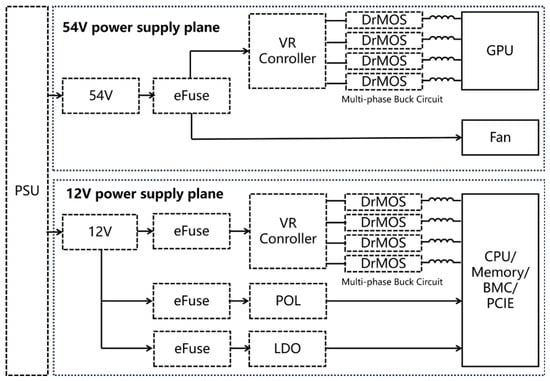
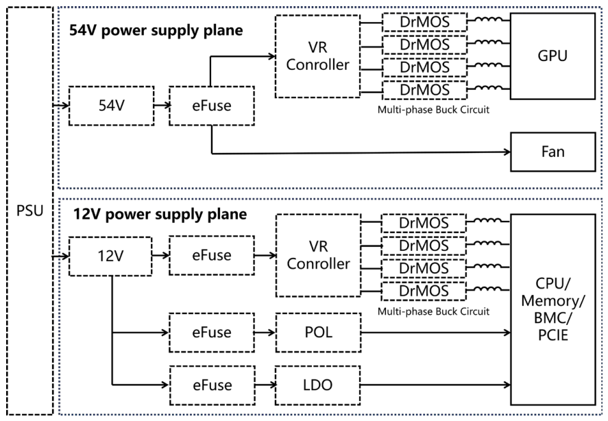
Based on the above analysis, this paper designs a hierarchical multi-phase parallel DC power supply system, as illustrated in Figure 1. Its core design philosophy is to divide different power planes within the entire AI server according to the power consumption levels and electrical characteristics of varying loads, implementing differentiated power supply strategies. Specifically, for traditional low-power loads such as CPUs, memory, hard drives, BMC, and PCIe, the standard 12 V supply voltage is maintained. This is primarily because the power consumption of conventional loads is relatively low, and current levels under 12 V power supply remain within acceptable limits without needing to introduce the additional design complexity associated with high-voltage power supply; simultaneously, the 12 V power architecture is highly mature in the general-purpose server sector, and adopting multi-phase power parallel supply schemes can achieve low-cost, high-reliability design goals. For high-power loads such as GPUs and cooling fans, a 54 V high-voltage DC power supply is utilized. High-voltage DC power effectively reduces transmission current, substantially lowering energy losses along the power delivery path, thereby improving energy utilization efficiency. Under the 54 V power architecture, the current density of the transmission path drops, leading to correspondingly reduced current-carrying requirements for connectors and PCB routing, which helps enhance the overall reliability and power density of the power supply system. Within each voltage plane, multi-phase parallel load-balancing technology is applied; all phase circuits operate simultaneously, and accurate equalization of the load current for each phase is achieved through current balancing algorithms built into the controller. This technical strategy not only further mitigates thermal losses but also suppresses current ripple and enhances dynamic response capability, providing a stable DC voltage for the loads. The hierarchical multi-phase parallel DC power delivery technology breaks through the current-carrying limits of traditional motherboard-level systems, demonstrating advantages in reducing transmission losses, improving power supply density, and enhancing power efficiency, thereby providing key technical support for the performance enhancement of AI servers.
Figure 1.
Schematic diagram of the power supply architecture.
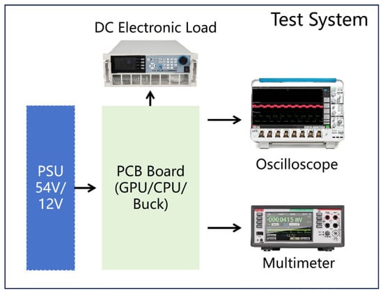
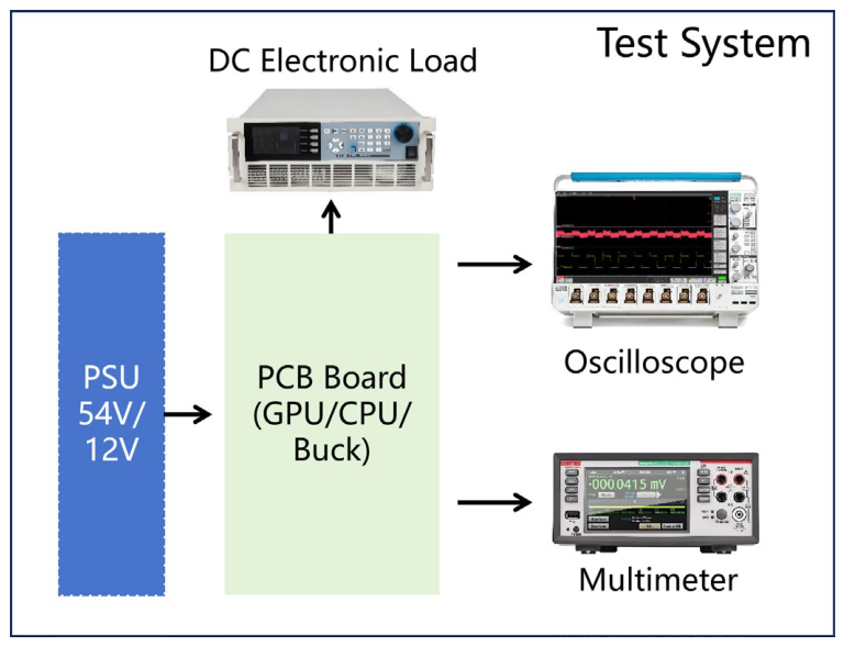
To comprehensively evaluate the actual performance of the hierarchical multi-phase parallel DC power supply system, a complete test system was constructed in this paper. The server converts AC power into DC power via the PSU, which serves as the initial energy source for the entire machine’s power supply. It should be noted that three-phase AC power distribution is an important approach for facility-level and rack-level power delivery. Under balanced three-phase voltage and current conditions, three-phase power transmission can reduce line current and improve power transmission efficiency compared with single-phase power supply. However, the focus of this work is the downstream DC power delivery architecture inside the AI server after AC-DC conversion by the PSU. Therefore, the proposed 54 V/12 V dual-plane DC architecture is located at the server-side DC distribution stage and can be used with PSUs supplied by either single-phase or three-phase AC sources. Multi-phase Buck power modules across different voltage planes further convert the high-voltage DC power into the working voltages required by loads, driving computing components like CPUs and GPUs to begin operations. Oscilloscopes are used to capture real-time power signal waveforms at key nodes, including output voltage ripple, jitter waveforms, and load transient response characteristics; multimeters are employed to precisely measure the DC voltage and operating current of the power supply system. By combining the measurement data from these two types of instruments, a systematic and comprehensive evaluation of the power architecture’s efficiency, dynamic response performance, and stability can be conducted. Test results indicate that this power architecture exhibits good efficiency levels and stable output characteristics under full-load operating conditions, meeting the engineering application requirements for AI servers.
The experimental system is shown in Figure 2. The PSU provides either 54 V or 12 V power input for different power planes. The oscilloscope is used to capture ripple and dynamic response waveforms, while the multimeter is used to record voltage and current data. The DC electronic load is used to emulate load variations. The power controller IC and DrMOS devices are both self-developed models. An 8-phase configuration is adopted, and the switching frequency is 600 kHz.
Figure 2.
Schematic diagram of the test system.
In the Buck converter circuit, a 0.1 μH TLVR inductor is selected at the output stage of each phase. The low inductance value helps improve the current slew-rate capability of the power stage, enabling faster current response during rapid load transients. Meanwhile, the TLVR structure enhances the coordination among multiple phases and accelerates transient current compensation, thereby reducing voltage undershoot and overshoot under dynamic load-step conditions. For the output capacitor network, multiple capacitors with different capacitance values, including 0.1 μF, 47 μF, 270 μF, and 470 μF, are connected in parallel. This hybrid capacitor configuration provides broadband decoupling capability: the 0.1 μF capacitors are mainly used to suppress high-frequency switching noise, the 47 μF capacitors provide medium- and high-frequency transient support, while the 270 μF and 470 μF bulk capacitors provide low-frequency energy buffering during large load variations. Therefore, the combined output capacitor network can reduce the equivalent output impedance over a wide frequency range, suppress output ripple, and improve the dynamic stability of the Buck converter.
The PCB is a self-developed board, and all experiments are conducted at an ambient temperature of 25 °C. The specific models of the instruments and equipment are summarized in Table 1.
Table 1.
Instrument List.
3. Results and Discussion
As the core component for achieving high-efficiency power supply in the hierarchical multi-phase parallel DC power system, the performance of the multi-phase Buck circuit directly influences the reliability and efficiency of the entire power delivery system. The controller is used to manage the switching actions of each phase’s power chips, regulating the output voltage magnitude by adjusting the duty cycle of the PWM signals, and is responsible for coordinating the phase relationships among all phases.
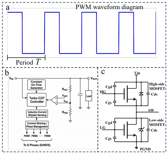
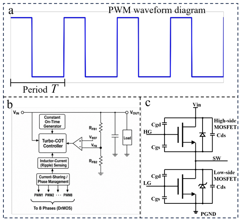
The DC-DC multi-phase step-down controller designed in this paper is responsible for uniformly regulating the switching sequence of each phase’s power chips, with its core regulation mechanism established on Pulse Width Modulation (PWM) technology. As shown in Figure 3a, the controller achieves closed-loop control of the output voltage amplitude by adjusting the duty cycle of each phase’s PWM signals; simultaneously, it manages the phase distribution relationships among all phases in real-time, ensuring a uniform distribution of the total load current across the parallel phases. This approach mitigates single-phase conduction losses and the risk of localized thermal stress concentration, enhancing the operational lifespan and system reliability of the entire power distribution network.
Figure 3.
Schematic diagram of the multi-phase Buck circuit. (a) PWM square wave signal diagram. (b) multi-phase power controller Turbo-COT schematic diagram. (c) DrMOS schematic diagram.
This controller incorporates Turbo-COT (Constant On-Time) control technology to overcome the inherent bottleneck in loop response speed found in traditional voltage-mode or current-mode PWM control, as illustrated in Figure 3b. The core of the Turbo-COT control strategy lies in fixing the conduction time of the power switches to a constant value, realizing continuous regulation of the duty cycle solely by adjusting the off-time. Firstly, the constant on-time architecture omits the oscillator charging and discharging processes typical of traditional PWM controllers, accelerating loop response speed and suppressing the jitter amplitude of the system output voltage during load transients. Secondly, the rapid loop response endows the controller with enhanced common-mode noise attenuation capabilities, improving the system’s stable operational ability in complex electromagnetic environments. Finally, this control technology facilitates balanced current sharing among phases, further strengthening the thermal equilibrium characteristics and long-term operational reliability of multi-phase systems.
At the power device level, the DC-DC power MOS chip utilized in this design internally integrates both High-side and Low-side MOSFETs. As shown in Figure 3c, compared to discrete MOSFET devices, this integrated MOSFET device not only saves layout area but also optimizes parasitic parameters in the power loop. It boasts numerous advantages, including low conduction internal resistance, fast switching speed, simplified driving circuits, and high conversion efficiency. The reduction in conduction internal resistance directly diminishes conduction losses from a physical mechanism standpoint; the short switching time controls switching losses and dynamic power consumption caused by the Miller effect; and the low parasitic inductance and capacitance decrease voltage and current overshoots during switching transients. Consequently, it elevates the system’s power conversion efficiency, reduces ripple, and enhances dynamic response.
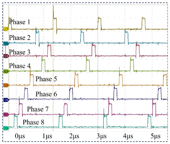
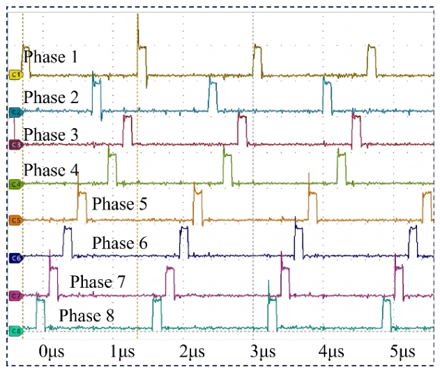
To verify the normal operational capability of the designed 8-phase parallel Buck circuit, a systematic test was conducted on the generation and output of the 8-phase PWM driving signals. As shown in Figure 4, the oscilloscope measurements clearly present 8 channels of PWM waveforms, with each channel sequentially phase-shifted by approximately π/4 (45°), yielding a total switching frequency of 600 kHz. Experimental results demonstrate that under the unified dispatch of the multi-phase DC-DC controller designed in this paper, all 8 power stages operate simultaneously and stably. The phase relationships of the PWM signals for each phase are precisely controllable, and no phase collision or timing disorder phenomena are observed, confirming the feasibility of the designed 8-phase Buck circuit and its engineering practical value in high-frequency, high-efficiency power conversion applications.
Figure 4.
Schematic diagram of 8-phase simultaneous operation.
In high-performance AI server systems, the power delivery networks of core processors (such as GPUs and CPUs) impose stringent physical requirements on the purity of the output steady-state voltage. If the amplitude of minute voltage ripples under steady-state conditions goes out of control, it will directly consume the logic gate noise margins within the chips, triggering unpredictable timing errors and computational faults, and the accompanying high-frequency alternating currents will accelerate the electromigration effects of micro-interconnects inside the semiconductor, shortening the physical lifespan of expensive computing chips. Therefore, the system-level capability to suppress steady-state ripple represents a core dimension for evaluating advanced DC-DC power architectures.
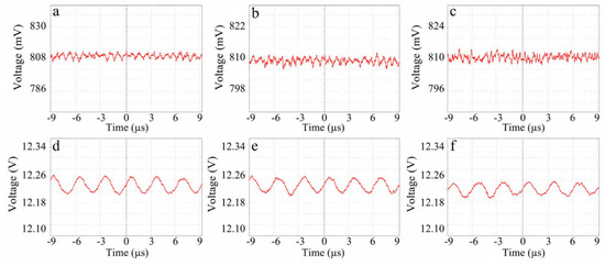
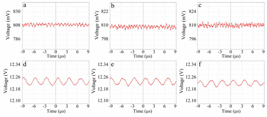
The steady-state ripple test results, as shown in Figure 5, reveal the capabilities of the two power planes in suppressing power supply noise. For the 12 V power plane, under steady-state conditions of 0 load, 50% load, and 100% load, its output ripple voltage fluctuation amplitudes (PK-PK) reached ±0.67%, ±0.68%, and ±0.66%, respectively. This fluctuation range has been restricted within the industry’s commonly required 1% baseline; however, in power supply scenarios for advanced process chips featuring low voltages and high currents, this absolute fluctuation of nearly ±0.7% represents non-negligible electromagnetic energy oscillation. The physical root of this fluctuation is that when the 12 V bus outputs hundreds of kilowatts of power, it must carry massive transmission currents on the motherboard PCB’s power delivery network (PDN). High-intensity alternating currents couple high-frequency voltage drops on the equivalent series inductance (ESL) and equivalent series resistance (ESR) of the filter capacitors, forming distinct switching noise envelopes.
Figure 5.
Ripple voltage performance of 12 V and 54 V power planes. Ripple voltage performance of the 12V power plane under (a) No-load. (b) 50% load. (c) 100% load conditions. Ripple voltage performance of the 54 V power plane under (d) No-load. (e) 50% load. (f) 100% load conditions.
The 54 V power plane exhibits steady-state ripple performance under the same load steps (0, 50%, 100%). Its measured ripple voltage fluctuation amplitudes (PK-PK) are compressed to ±0.26%, ±0.23%, and ±0.22%, respectively. This minute fluctuation level indicates that the 54 V hierarchical architecture enhances the purity of core power delivery.
This ripple suppression capability deeply relies on the precise execution of multi-phase Interleaving technology. Under the unified dispatch of the controller, the 8-phase Buck power stages operate stably and simultaneously, and the PWM waveforms of each phase channel are subjected to precise π/4 phase-shift regulation. When the AC ripple components of the inductor currents of each phase converge at the final output node, destructive interference occurs. This physical waveform superposition interference effect leaps the equivalent frequency of the synthesized total current ripple to eight times the single-phase switching frequency and cancels out the geometric amplitude of the ripple. Notably, transitioning from 0 light load to 100% full load, the ripple amplitude of the 54 V plane does not diverge with the increasing current; instead, it steadily converges at around ±0.22%. This confirms that the designed closed-loop system and current balancing algorithm can maintain electrical symmetry under all operating conditions, providing reliable power quality for high-density computing clusters.
To make the steady-state ripple results in Figure 5 easier to interpret, the detailed measurement conditions and quantitative ripple values are summarized in Table 2.
Table 2.
Summary of test conditions and measured performance of the 12 V and 54 V power planes.
When large AI models execute core algorithms of the Transformer architecture (such as large-scale general matrix multiplication, GEMM), the power consumption of computing chips exhibits extreme burstiness, high concurrency, and discontinuity. Server GPUs often complete an instantaneous transition from a low-frequency idle state to a full-speed full-load state within an extremely short period of a few microseconds. This load current impact with an extremely high slew rate (di/dt) serves as a dynamic test for the transient response capability of the power delivery network. If the energy replenishment of the power converter is delayed, the massive current deficit will cause a deep undershoot in the output voltage; conversely, when the computing task is instantaneously unloaded, the energy in the inductor that cannot be released in time will trigger a voltage overshoot.
Furthermore, the current-sharing performance of the 8-phase parallel system can be analytically validated through the synchronized behavior of the phase timing and the output ripple envelope. Mechanistically, a balanced current distribution among parallel channels is a direct functional product of precise phase interleaving and stable loop regulation. As demonstrated in the π/4 (45°) sequentially phase-shifted driving waveforms in Figure 4, the structural symmetry of the control loops guarantees temporal equilibrium among the active channels. This temporal symmetry is further corroborated by the steady convergence of the 54 V plane’s steady-state ripple down to ±0.22% at full load. Because complete destructive cancellation of current ripples requires absolute mathematical alignment of both phase angles and current amplitudes at the converging output node, the absence of ripple divergence under peak workloads implicitly confirms that the multi-phase current balancing algorithm maintains stringent electrical symmetry under all operating conditions.
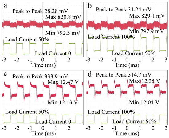
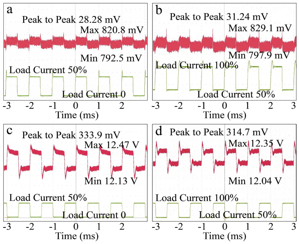
For the 12 V power plane, experiments separately recorded the voltage responses under 0–50% load steps and 50–100% load steps, as shown in Figure 6a,b. Test data reveal that under the 0–50% dynamic load variation, the peak-to-peak (PK-PK) fluctuation amplitude of the output voltage is ±2.36%, whereas under the 50–100% load variation, the fluctuation amplitude is ±1.83%. The relatively larger fluctuation amplitude generated by the 0–50% step is attributed to the system’s starting point at zero or light-load conditions. Under light-load conditions, the multi-phase Buck circuit may operate in discontinuous conduction mode (DCM) or maintain operation with only a small number of phases through phase-shedding control to reduce switching losses. When the load instantaneously surges to 50%, the control loop needs to rapidly increase the duty cycle and undergo a transition from discontinuous mode to continuous conduction mode (CCM) or wake up dormant phases. During this settling time, the output capacitor must independently bear the entire load current, resulting in a more pronounced voltage drop. In contrast, the 50–100% step is conducted when the system is already under steady-state high-current conditions, where the base inductor current is higher and all phases are active, rendering the physical delay of loop adjustments minor.
Figure 6.
Dynamic load-step response of the 12V and 54 V power planes. (a) 12 V plane under 0–50% load step. (b) 12 V plane under 50–100% load step. (c) 54 V plane under 0–50% load step. (d) 54 V plane under 50–100% load step.
For the 54 V power plane, load step test results under the same conditions are shown in Figure 6c,d. During a 0–50% load variation, the voltage fluctuation amplitude PK-PK is ±1.42%; during a 50–100% load variation, the fluctuation amplitude is ±1.33%. Compared to the 12 V plane data, the 54 V plane demonstrates a narrower voltage deviation range. The engineering rationale behind this phenomenon mainly involves the impedance characteristics and transformation ratio effects of the power delivery network (PDN). According to Faraday’s law of electromagnetic induction, because the voltage of the 54 V supply bus is higher than 12 V, when providing the same output power step, the absolute current variation on the bus side (primary side) is compressed to approximately one-fourth. This implies that along the same parasitic inductance path, the induced voltage drop generated by the 54 V system is proportionally reduced, thereby alleviating the transient voltage drop at the physical level.
Furthermore, the Turbo-COT control technology employed in this study plays a critical regulatory role in both voltage planes. This control strategy bypasses the complex compensation network calculations found in traditional PWM control by fixing the conduction time and adjusting the off-time in real-time. When output voltage drops due to load transients are detected, the nonlinear ramp generation circuit can immediately trigger the conduction of the next cycle, pumping charge to the output terminal at an extremely high sampling frequency. Equipped with a higher primary-side voltage reserve, the 54 V plane, combined with the response of Turbo-COT, can more rapidly compensate for the current deficit on the output side. Synthesizing the experimental phenomena, dynamic response performance is influenced by control algorithms and is dependent on the physical voltage level of the supply bus and its dampening effect on the current slew rate of transmission links.
When evaluating the comprehensive performance of server power delivery architectures, conversion efficiency is a core metric for measuring power conversion losses and directly determines the thermal management difficulty and reliability of the entire system.
Efficiency (η) can be expressed as Equation (1):
In Equation (1), Pout is the output power, which is calculated based on the output current Iout and output voltage Vout. Pin is the input power, which is calculated based on the input current Iin and input voltage Vin.
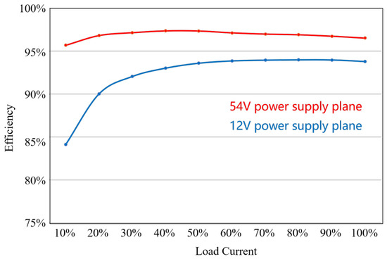
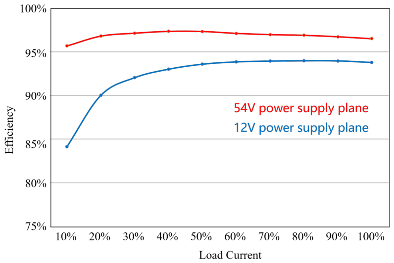
For high-power AI servers, since the power consumption of a single machine has reached the scale of several kilowatts, every percentage point of efficiency improvement in the power supply link can significantly reduce waste heat emission. Efficiency comparison test results are shown in Figure 7, illustrating the energy efficiency differences between the 54 V power plane and the 12 V power plane across the entire load range. The efficiency curves depicted in Figure 7 represent the measured averages derived from 5 independent sequential test runs, where the standard deviation at each loading point remains below 0.05% due to the high test repeatability and instrument precision. From the measured curves, it can be seen that within the 10% to 100% load range, the conversion efficiency of the 54 V power plane is consistently higher than that of the 12 V plane. Specifically, the peak efficiency of the 54 V power plane reaches approximately 97%, and it exhibits highly flat energy efficiency characteristics within the medium-to-high load range of 40% to 90%. In comparison, the maximum efficiency of the 12 V power plane is approximately 94%, and upon entering the high-load region, its efficiency curve exhibits a decline due to exacerbated conduction losses caused by high currents. The core scientific basis for this generational leap in energy efficiency lies in the physical compression of transmission currents by the hierarchical architecture. According to Joule’s law, P = I2R, conduction losses in the power delivery network (PDN) are proportional to the square of the current. This “high-voltage, low-current” transmission mode can substantially reduce the ideal bus-distribution I2R loss component. By resolving the loss challenges brought about by high currents from the underlying architecture, the system eliminates the thermal accumulation phenomena present in traditional architectures, clearing physical obstacles for improving power density.
Figure 7.
Schematic diagram of efficiency for 54 V and 12 V power planes.
To evaluate the impact of the switching devices’ non-zero on-resistance (RDS(on)) on efficiency, the total conduction loss (Pcond) within the 8-phase DrMOS stage can be expressed as Equation (2):
where N = 8 is the phase count, RDS(on) represents the non-zero internal resistance of High-side/Low-side MOSFETs, and Irms is the root-mean-square current per phase. Because of the non-zero RDS(on), conduction losses scale quadratically with the operating current. In the traditional 12 V plane, heavy current levels cause high I2×RDS(on) thermal dissipation, degrading high-load efficiency. Conversely, the 54 V architecture reduces the line current by approximately 4.5 times for equivalent power delivery, exponentially suppressing the loss penalty induced by this non-zero resistance. Additionally, the multi-phase parallel configuration evenly fractions the total current, keeping each DrMOS chip within its optimal, lowest-resistance thermal zone.
Moreover, the efficiency improvement benefits from the deep synergy between multi-phase parallel technology and DrMOS chips. multi-phase parallel load-balancing technology accurately distributes the total current to each phase through the current-sharing algorithm built into the controller. This avoids the risk of the conduction internal resistance RDS (on) of single-phase power devices deteriorating sharply with rising temperatures due to current overshoots under heavy loads, ensuring the system operates within the thermal safe zone and optimal efficiency point of the devices. Meanwhile, because the utilized DrMOS integrates optimized power transistors and drive circuits, its remarkably low parasitic inductance significantly reduces switching losses during high-frequency switching processes. Comprehensive experimental results prove that the 54 V hierarchical power delivery architecture provides a potential power-delivery approach for improving server-level energy efficiency; however, complete server-level and data-center-level PUE evaluation requires further system-level validation.
To provide a consolidated summary of the experimental results, the key test conditions and measured performance of the 12 V and 54 V power planes are summarized in Table 2. The table includes the input voltage, output voltage, output current, output power, ripple voltage, transient deviation, and conversion efficiency under the tested load conditions. This summary allows a more direct comparison between the two power planes and provides a quantitative basis for evaluating the effectiveness of the proposed hierarchical 54 V/12 V dual-plane power delivery architecture.
4. Conclusions
To overcome the physical limitations in efficiency and heat dissipation of traditional power architectures in high-density AI servers, this paper proposes and evaluates a hierarchical 54 V/12 V dual-plane multi-phase DC power delivery architecture. By implementing a high-voltage power distribution strategy, the system successfully resolves critical challenges faced by traditional 12 V networks, such as high conduction losses and transient instability. Experimental evaluations confirm that the proposed architecture achieves performance improvements. The 54 V power plane demonstrates excellent steady-state and dynamic characteristics, not only controlling the steady-state ripple fluctuation of the output voltage to within ±0.26%, but also restricting transient voltage fluctuations to a range of ±1.42% under severe load step impacts. From a scientific standpoint, the 54 V power distribution network substantially reduces conduction losses in transmission links compared to the 12 V system, enabling the system’s peak conversion efficiency to reach approximately 97%. This improvement is important for mitigating localized hotspot effects on high-power server motherboards. In summary, the integration of hierarchical power planes, multi-phase interleaving technology, and Turbo-COT control strategies provides a highly scalable and robust solution for meeting modern high-computing-power demands. This research enhances the operational stability and comprehensive energy efficiency of individual AI servers, and aligns with the development trends of green, sustainable computing infrastructure, opening up a practical evolutionary path for optimizing overall energy consumption metrics in data centers. Nevertheless, certain limitations of the current study should be acknowledged. The empirical evaluation is primarily conducted on a laboratory experimental prototype under synthetic load-step conditions. Future work will focus on expanding this validation framework to encompass full-scale server operations, long-term component reliability testing, and profiling under real-world dynamic AI workloads such as large language model training and inference tasks.
Author Contributions
S.X.: conceptualization, formal analysis, investigation, methodology, visualization, writing—original draft, and writing—review and editing; H.Y.: conceptualization and formal analysis; Y.L.: visualization; W.L.: investigation and methodology; R.Z.: writing—review and editing and supervision. All authors have read and agreed to the published version of the manuscript.
Funding
This work was supported by the Ministry of Industry and Information Technology of the People’s Republic of China, the Distributed Acceleration Server Project (Grant No. 6000052/RD3800240002), and the Shandong Provincial Natural Science Foundation (Grant No. ZR2025QC1862Z).
Data Availability Statement
The original contributions presented in this study are included in the article. Further inquiries can be directed to the corresponding authors.
Conflicts of Interest
Author Shaohang Xu was employed by Inspur Computer Technology Co., Ltd. The remaining authors declare that the research was conducted in the absence of any commercial or financial relationships that could be construed as a potential conflict of interest.
References
- Cooper, A.I.; Courtney, P.; Darvish, K.; Eckhoff, M.; Fakhruldeen, H.; Gabrielli, A.; Garg, A.; Haddadin, S.; Harada, K.; Hein, J.; et al. Accelerating discovery in natural science laboratories with AI and robotics: Perspectives and challenges. Sci. Robot. 2025, 10, eadv7932. [Google Scholar] [CrossRef] [Scilit] [PubMed]
- Kalluri, P.R.; Agnew, W.; Cheng, M.; Owens, K.; Soldaini, L.; Birhane, A. Computer-vision research powers surveillance technology. Nature 2025, 643, 73–79. [Google Scholar] [CrossRef] [Scilit] [PubMed]
- Anjum, M.; Shahab, S. Improving autonomous vehicle controls and quality using natural language processing-based input recognition model. Sustainability 2023, 15, 5749. [Google Scholar] [CrossRef] [Scilit]
- Radanliev, P.; De Roure, D.; Maple, C.; Santos, O. Forecasts on future evolution of artificial intelligence and intelligent systems. IEEE Access 2022, 10, 45280–45288. [Google Scholar] [CrossRef] [Scilit]
- Jonnalagadda, A.M.C. Artificial Intelligence for Autonomous Infrastructure: A Deep Reinforcement Learning Approach to Datacenter Operations. Int. J. Res. Appl. Innov. 2025, 8, 13022–13034. [Google Scholar] [CrossRef] [Scilit]
- Hua, H.; Li, Y.; Wang, T.; Dong, N.; Li, W.; Cao, J. Edge computing with artificial intelligence: A machine learning perspective. ACM Comput. Surv. 2023, 55, 1–35. [Google Scholar] [CrossRef] [Scilit]
- Cruzes, S. Data centers in the age of AI: A tutorial survey on infrastructure, sustainability, and emerging challenges. J. Netw. Comput. Appl. 2026, 252, 104525. [Google Scholar] [CrossRef] [Scilit]
- Chen, Y.; Shi, K.; Chen, M.; Xu, D. Data center power supply systems: From grid edge to point-of-load. IEEE J. Emerg. Sel. Top. Power Electron. 2022, 11, 2441–2456. [Google Scholar] [CrossRef] [Scilit]
- Ahmed, K.M.U.; Bollen, M.H.J.; Alvarez, M.; Letha, S.S. The impacts of voltage disturbances due to faults in the power supply system of a data center. In Proceedings of the 2022 20th International Conference on Harmonics & Quality of Power (ICHQP), Naples, Italy, 29 May–1 June 2022; IEEE: New York, NY, USA, 2022; pp. 1–6. [Google Scholar]
- Li, F.; Zhu, J.; Yu, L.; Nie, C.; Ma, C.; Wang, J. A Modularized Partial Power Converter Based Uninterruptible Power Supply Scheme for DC Power Feeding Servers in Data Centers. IEEE Trans. Power Electron. 2025, 41, 5486–5498. [Google Scholar] [CrossRef] [Scilit]
- Ahmed, K.M.U.; Alvarez, M.; Bollen, M.H.J. Reliability analysis of internal power supply architecture of data centers in terms of power losses. Electr. Power Syst. Res. 2021, 193, 107025. [Google Scholar] [CrossRef] [Scilit]
- Sorouri, H.; Sedighizadeh, M.; Oshnoei, A.; Khezri, R. An intelligent adaptive control of DC–DC power buck converters. Int. J. Electr. Power Energy Syst. 2022, 141, 108099. [Google Scholar] [CrossRef] [Scilit]
- Lu, Y.; Huang, J.; Tong, Z.; Hu, T.; Zeng, W.-L.; Huang, M.; Mao, X.; Cai, G. An overview of hybrid DC–DC converters: From seeds to leaves. IEEE Open J. Solid-State Circuits Soc. 2023, 4, 12–24. [Google Scholar] [CrossRef] [Scilit]
- Acosta-Rodríguez, R.A.; Rosero-García, J.; Rivera, M.; Chaimanekorn, K. Recent Advances in Non-Isolated DC/DC Converter Topologies: A Review and Future Perspectives. Appl. Sci. 2025, 15, 12868. [Google Scholar]
- Koh, S.T.; Bae, S. Research Trends and Challenges of Integrated Constant On-Time (COT) Buck Converters. Electronics 2025, 14, 3721. [Google Scholar] [CrossRef] [Scilit]
- Litrán, S.P.; Durán, E.; Semião, J.; Díaz-Martín, C. Multiple-output DC–DC Converters: Applications and solutions. Electronics 2022, 11, 1258. [Google Scholar] [CrossRef] [Scilit]
- Omar, F.A. Comprehensive analysis and evaluation of DC-DC converters: Advancements, applications, and challenges. Black Sea J. Eng. Sci. 2023, 6, 557–571. [Google Scholar] [CrossRef] [Scilit]
- Patel, P.; Gong, Z.; Rizvi, S.; Choukse, E.; Misra, P.; Anderson, T.; Sriraman, A. Towards improved power management in cloud gpus. IEEE Comput. Archit. Lett. 2023, 22, 141–144. [Google Scholar] [CrossRef] [Scilit]
- Yang, Z.; Adamek, K.; Armour, W. Accurate and convenient energy measurements for gpus: A detailed study of nvidia gpu’s built-in power sensor. In Proceedings of the SC24: International Conference for High Performance Computing, Networking, Storage and Analysis, Atlanta, GA, USA, 17–22 November 2024; IEEE: New York, NY, USA, 2024; pp. 1–17. [Google Scholar]
- Jay, M.; Ostapenco, V.; Lefèvre, L.; Trystram, D.; Orgerie, A.-C.; Fichel, B. An experimental comparison of software-based power meters: Focus on CPU and GPU. In Proceedings of the 2023 IEEE/ACM 23rd International Symposium on Cluster, Cloud and Internet Computing (CCGrid), Bangalore, India, 1–4 May 2023; IEEE: New York, NY, USA, 2023; pp. 106–118. [Google Scholar]
- Krzywaniak, A.; Czarnul, P.; Proficz, J. Dynamic GPU power capping with online performance tracing for energy efficient GPU computing using DEPO tool. Future Gener. Comput. Syst. 2023, 145, 396–414. [Google Scholar] [CrossRef] [Scilit]
- Khan, I.; Rahman, S.; Ayaz, M.A.; Amir, M.; Shehada, H. Review of Isolated DC-DC Converters for Application in Data Center Power Delivery. IEEE Trans. Ind. Appl. 2024, 60, 55436–55446. [Google Scholar] [CrossRef] [Scilit]
- He, J.-P.; Liu, X.-R.; Xia, Y.-K.; Chen, Y.-Q.; Wu, C.-D. A voltage ripple compensation method for constant on-time buck converter. IEEE Access 2023, 11, 139628–139642. [Google Scholar] [CrossRef] [Scilit]
- Chen, K.; Garrett, J.; Peng, K.; Hulfachor, R.; Onabajo, M. Buck circuit design with pseudo-constant frequency and constant on-time for high current point-of-load regulation. IEEE Trans. Circuits Syst. I Regul. Pap. 2021, 68, 4062–4075. [Google Scholar]
- Liu, P.J.; Kuo, M.H. Adaptive on-time buck converter with wave tracking reference control for output regulation accuracy. Energies 2021, 14, 3809. [Google Scholar] [CrossRef] [Scilit]

Disclaimer/Publisher’s Note: The statements, opinions and data contained in all publications are solely those of the individual author(s) and contributor(s) and not of MDPI and/or the editor(s). MDPI and/or the editor(s) disclaim responsibility for any injury to people or property resulting from any ideas, methods, instructions or products referred to in the content. |
© 2026 by the authors. Licensee MDPI, Basel, Switzerland. This article is an open access article distributed under the terms and conditions of the Creative Commons Attribution (CC BY) license.