


Abstract
This work presents an integrated methodology for modeling, parameter tuning, and experimental emulation of Dual Active Bridge (DAB) converters aimed at detailed simulation, control design, and real-time emulation. This is needed to bridge the gap between theoretical modeling and practical implementation, enabling accurate prediction of converter behavior under realistic operating conditions and facilitating the development of control strategies. The study begins with the derivation of a nonlinear model including parasitic elements and transformer characteristics, enabling accurate representation of the converter’s dynamics across operating conditions. To address deviations caused by component tolerances, the model parameters are calibrated using a multi-algorithm optimization framework based on Particle Swarm Optimization, Grey Wolf Optimizer, Secretary Bird Optimization, and Whale Optimization, where the error between predicted and experimental waveforms is minimized. The comparative analysis allows selecting the most suitable optimization strategy based on statistical analyses. The model is also discretized and implemented on a Hardware-in-the-Loop (HIL) platform based on a high-performance microcontroller, enabling real-time emulation of the converter as a digital twin. Moreover, a control-oriented version of the model is presented and used to design a voltage controller, which is subsequently tested in both the HIL environment and on a real DAB converter prototype. Experimental results report differences between HIL and real prototype below 3.9% for currents and 4.45% for voltages in multiple operation conditions, demonstrating an accurate representation of the real power system. This methodology ensures low errors between theoretical, simulated, and experimental behavior, providing a framework for accurate modeling and controller design of DAB converters.
1. Introduction
The Dual Active Bridge (DAB) converter is one of the most widely adopted isolated bidirectional DC–DC topologies in energy storage systems, electric vehicles, and modern DC networks [1,2]. Such a predilection is based on the DAB converter advantages: high efficiency, high power density, bidirectional power flow capability, galvanic isolation, and soft switching (ZVS). However, precise modeling of the DAB converter remains a challenge due to its strong nonlinear behavior and the interdependence among multiple design parameters, which has driven the evolution of models from idealized approximations to high-fidelity mathematical formulations.
Early model developments relied on simplified representations that neglected losses and parasitics, providing analytical expressions of transferred power as a function of the phase shift between bridges, particularly under single-phase-shift (SPS) modulation. Although applicable for preliminary design, such models show significant limitations in predicting efficiency and control behavior, as they disregard practical effects such as switching and conduction losses or leakage inductances [3].
A significant advance was made by Krismer and Kolar, who developed a detailed model that includes conduction and switching losses in the semiconductors, magnetic core losses, and parasitic resistances, demonstrating that idealized formulations underestimate total system dissipation [4]. For high-power applications, such as automotive converters or bidirectional DC network interfaces, those detailed models are essential for accurately estimating efficiency. More recently, Vardhan et al. analyzed the influence of finite magnetizing inductance, demonstrating that ignoring such an effect alters the resonant behavior and can lead to transformer oversizing [5]. The model proposed in this work integrates both leakage and external inductances, providing more accurate tools for electromagnetic and thermal optimization.
The evolution of average models has led to more generalized and accurate formulations. For example, Liu et al. in [6] introduced the enhanced generalized average model (EGAM), which incorporates additional harmonic components beyond traditional generalized average models (GAMs), thereby improving the prediction of dynamic response. Chakraborty et al. proposed a high-precision GAM that includes high-frequency terms to better capture transient behavior [7]. Veeramraju and Kimball extended this approach to AC-DC converters using a multi-frequency EGAM, capable of modeling the interaction between the grid and switching elements using discrete convolutions in the frequency domain, thus overcoming the limitations of conventional and 2D-GAM models [8].
Dynamic small-signal modeling has also proven essential for the design of classical controllers. Rajender et al. [9] developed a small-signal model for EV chargers based on DAB converters using state-space averaging and Fourier expansion, enabling the design of Proportional–Integral (PI) controllers that ensure stability across multiple charging modes (CC, CV, CCCV). On the other hand, Dubey and Lakshminarasamma focused on the series-resonant DAB (SRDAB) converter, formulating a GAM that includes the resonant capacitor voltages and inductor current, effectively capturing the beat-frequency phenomena and providing a small-signal basis for control design under phase-shift modulation [10].
The DAB converter has been used in a range of applications, from renewable energy systems to electric vehicle charging and energy storage interfaces. One prominent application is photovoltaic generation, where the DAB converter has been identified as a suitable solution due to its high efficiency, galvanic isolation, and wide voltage conversion range. Recent contributions have addressed design-oriented approaches that consider PV generator interaction for maximum power extraction through appropriate selection of transformer turns ratio and leakage inductance [11], control-oriented linearized models that facilitate classical controller design and stability analysis [12], and advanced cascade structures with adaptive regulation for robust maximum power point tracking under varying conditions [13]. These complementary efforts underscore the importance of an integrated approach combining design, modeling, and control. Another common scenario where the DAB model plays a critical role is controller design. The availability of accurate models has enabled more reliable control strategies, with PI and PID controllers remaining predominant when supported by calibrated representations of system gain and phase [14]. Model-based predictive voltage control schemes complemented by disturbance observers have achieved superior speed and robustness compared to conventional methods [15].
Given the wide variety of models used in the literature, the accuracy of DAB converter parameter estimation is a fundamental pillar for the simulation and design of controllers that are not robust (i.e., sensitive to parameter deviations) but offer high performance. While simplified models neglect losses, leakage inductance, or thermal effects, classical controllers based on generalized averaging (or small-signal theory) require precise knowledge of resistances, parasitic capacitances, magnetic inductances, and core losses to ensure realistic phase and gain margins. A poor parameter estimation leads to suboptimal responses or instability.
To mitigate this problem, multiple parameter identification and calibration techniques, offline and online, have been applied to power converters. However, some methodologies can be hybrid in nature, that is, an offline preprocessing technique, like the Taguchi-ANOVA [16], combined with real-time parametric estimation. The methodology can be structured in two sequential phases: first, offline preprocessing (Taguchi), which defines orthogonal arrays to identify the converter’s critical parameters, followed by the percentage quantification of each parameter (ANOVA) based on the system’s responses (efficiency, transient response, frequency response). Then, the selection of parameters with a statistically significant contribution, and finally, the reduced model calculation. The second phase is executed in real-time, and consists of sampling the signals from the converter during operation (voltages, currents, temperature), then applying the dimensionality reduction defined in phase 1 to filter the input variables, next running a lightweight optimization algorithm on the reduced search space to estimate the current parameters, and finally incorporating the estimated parameters into the system.
However, offline optimization techniques have emerged as powerful tools for tuning model parameters based on experimental tests (transient response, frequency response, switched waveforms), as they enable the identification of the combination that minimizes the error between the simulation and the actual measurement. This ensures reliable predictive controllers with gains tuned to actual behavior, improving stability, bandwidth, and robustness, and thus bridging the gap between the theoretical model and the physical converter. This approach surpasses manual or linear identification by capturing nonlinearities and couplings. The selection of the optimization algorithm constitutes the first stage of this work.
The parameter estimation method must include a comparison of multiple optimization algorithms, ranging from gradient descent to metaheuristics such as PSO, GWO, SBOA, or WOA. This will avoid local minima and ensure the best possible representation of the physical converter, so that the model’s accuracy allows accurate simulations and the design of robust controllers in the classical sense, yet insensitive to parameter drifts thanks to a highly accurate base model.
However, research on optimizers for DAB converters has focused on three key areas: converter design optimization, controller design optimization, and parameter estimation optimization. The first area focuses on the converter and its parameters (transformation ratio, inductance, number of turns in the windings, and air gap length), using particle swarm optimization (PSO) algorithms, genetic algorithms, or MATLAB’s Fmincon (R2022a) function [17,18,19,20,21].
The second topic is controller optimization. In general, these studies aim to optimize the modulation variables to improve transient performance and efficiency. To this end, deep reinforcement learning (DRL) and numerical optimization routines are used to find modulation trajectories that minimize, for example, conduction losses [17,22,23,24,25,26,27].
Third, the approach used in the methodology proposed in this paper: optimization for estimating the converter parameters. This optimization process has received small attention in the literature, which has focused on identifying the series/leakage inductance, the capacitance and its equivalent series resistance, and the on-resistance (Ron) to improve controller accuracy and enable condition monitoring. The most commonly used optimizers are based on recursive least squares (RLS), particle swarm optimization (PSO), gradient descent, and genetic algorithms combined with neural networks (GA-BP) [23,24,25,27,28]. Those methods are primarily used for fault diagnosis, controller tuning, and modulation optimization.
The next step is to validate the hypothesis through a step-by-step process that ensures the system’s reliability, efficiency, and safety before its final implementation. This process is structured in four complementary stages: Software-In-the-Loop (SIL), Processor-In-the-Loop (PIL), Hardware-In-the-Loop (HIL), and experimental prototype validation. The SIL stage enables verification of the converter’s mathematical model and control strategy in a purely simulated environment, without interaction with physical hardware. Here, conceptual errors are detected, and parameters are adjusted without operational risks. Subsequently, in the PIL tests, the physical controller (such as a microcontroller or DSP) is introduced into the simulation, validating the real-time implementation of the algorithm and its interaction with the converter model. This stage reveals computational limitations and coding errors.
Next, HIL integrates precise emulation of the converter’s electrical dynamics with real-time controller operation. This allows the system’s behavior to be evaluated under extreme conditions or failures, without exposing expensive components to damage. Finally, experimental validation is performed with the complete prototype in actual operation, confirming performance under real conditions of load, ripple, thermal efficiency, and electromagnetic compatibility. Each stage is essential: SIL reduces initial costs, PIL ensures proper implementation of control software, HIL mitigates risks before physical assembly, and experimental validation verifies compliance with technical specifications. Together, those phases form a robust methodology that minimizes errors, accelerates development, and ensures quality in research on switched power converters.
Previous work in the literature focused on HIL platforms for the development of DAB converters primarily employs high-performance commercial solutions such as Typhoon HIL, OPAL-RT, RTDS, and PLECS RT Box [14,29,30,31,32,33]. Those technologies use real-time processors and FPGAs to achieve high-fidelity simulations, interacting with external controllers based on DSPs or microcontrollers such as the STM32F446RE [14,29,34,35,36].
The models simulated on those platforms are predominantly switched-mode, allowing frequencies of up to 200 kHz through optimization techniques such as “nanostep” or sub-cycle averaging in FPGAs [29,37]. High-fidelity models incorporate leakage inductance, dead times, and conduction losses, as well as thermal models of switches to bridge the gap between simulation and reality [29]. Furthermore, GAMs based on Fourier transforms have been implemented to design control gains [37,38] systematically.
The primary purpose of those platforms is to evaluate advanced control strategies (model predictive control (MPC), robust control, or reinforcement learning), optimize efficiency by reducing reactive power (backflow power), and validate protection systems in critical applications such as ultra-fast electric vehicle charging and microgrids [30,31,32,36,39,40].
A key aspect is the prior validation of those models against actual converters. While some platforms show a high degree of agreement with actual converters [29,31,32], considerable deviations due to unmodeled parasitic elements have also been identified.
In that context, this paper proposes an integrated methodology for the modeling, parameter tuning, and experimental validation of DAB converters models, which is aimed at real-time HIL emulation purposes. The discrete-time model is calibrated through PSO-based optimization to match the converter’s experimental responses. A second modeling approach, for control applications, is derived by truncating high-frequency components from the more accurate representation. That modeling approach is validated by designing a voltage controller, which is tested in both on the real converter and in a HIL platform running on a high-performance microcontroller.
The methodology process followed in this work starts from the detailed modeling of the converter (considering conduction losses) to the experimental validation of the model and control usefulness through real operation and HIL tests. Each stage was designed to ensure consistency among the theoretical model, the simulated behavior, and the experimental response of the system. This methodological approach ensured the accuracy and coherence of the model, as well as the robustness and practical feasibility of the designed control.
The rest of the paper is organized as follows. Section 2 describes the first stage of the methodological process, which includes the derivation of the mathematical model, the parameter identification and the model validation. Section 3 describes the model discretization and HIL implementation, which corresponds to stage 2 of the methodological process. Then, Section 4 presents stages 3 and 4, which derive a control-oriented version of the model to produce a transfer function suitable for control design; the usability of that transfer function is tested with a classical control design. Moreover, that control system is tested using both the developed HIL platform and a real DAB converter. Finally, the conclusions of the work close the paper.
2. Mathematical Model
Figure 1 shows the DAB converter used for the modeling stage. In this diagram, the converter is represented including all conduction losses associated with the power devices and passive components. This detailed representation enables the construction of a model that accurately describes the converter’s dynamic behavior across different operating conditions, serving as the foundation for subsequent stages of fitting, validation, and control design.
Figure 1.
DAB converter for photovoltaic and battery charger applications.
In the circuital scheme of Figure 1, the main power source is modeled using a Thevenin equivalent formed by a voltage source and its internal resistance , which supplies the input current . To smooth out voltage ripples, an input capacitor filter is connected at the low-side interface. The bidirectional core of the DAB converter comprises low-side () and high-side () full-bridges, each featuring four MOSFET switches driven by complementary gating signals. Interfacing both bridges, the high-frequency transformer assembly is represented by an ideal transformer with a turns ratio of 1:N, a leakage inductance , and a magnetizing inductance . Additionally, a series external inductance is incorporated into the primary side to adjust the power transfer capability. Finally, the high-voltage output stage considers a filtering capacitance connected in parallel with the load impedance, modeled by .
The previous circuital model does not account for switching losses, which can be significant in high-power, high-frequency systems that operate without soft-switching techniques. However, the simulation of this model remains widely applicable for several reasons that are worth highlighting. First, the absence of switching losses does not invalidate the use of the model for the design and validation of closed-loop control strategies. The fundamental dynamic phenomena of the converter, such as phase-angle-controlled power transfer, transient responses to load or voltage changes, and system stability, are governed primarily by the transformer’s electromagnetic parameters and leakage inductance, which are modeled in detail. Therefore, the model remains a valuable tool for evaluating controllers in high-power scenarios, where response times and stability margins are critical. Second, for systems that operate without soft-switching and at high frequencies (typically > 100 kHz), switching losses depend heavily on operating conditions (input voltage, load current, semiconductor temperature). Incorporating them into an averaged or small-signal model requires complex, device-specific empirical characterizations, which are often unavailable in the early stages of design. Therefore, this deliberately simplified approach provides a lower bound on efficiency and, more importantly, serves as a basis for adding experimentally calibrated switching-loss models without losing the model’s fundamental structure. Finally, in the context of parametric estimation via optimization, excluding switching losses reduces the number of parameters to be estimated, facilitates convergence, and allows the algorithms to focus their efforts on the precise identification of the electrical and magnetic parameters. Once this base model has been obtained, it is feasible to incorporate switching-loss blocks as external elements to the converter, e.g., using lookup tables or coupled thermal models, which are fed by the currents and voltages calculated by the model. In this way, the model becomes a core for fast electromagnetic simulation, to which additional layers of fidelity can be added without compromising numerical stability or real-time performance.
Recent studies [1] have proposed hybrid modulation techniques that combine PWM and optimal discrete PDM. This approach enables continuous output regulation, generation of symmetrical pulses, elimination of even subharmonics, and improved system efficiency. However, since one of the objectives of this paper is to demonstrate the benefits of the model-tuning technique, the adopted modulation scheme is shown in Figure 2. This figure illustrates the steady-state switching waveforms of the primary () and secondary () AC voltage profiles generated by and , respectively. Both operating signals are unipolar square waves shifting between logic levels 0 and 1 with a fixed 50% duty cycle to maximize power transfer efficiency [41]. The relative phase shift angle between the two bridges, denoted by , varies continuously within the range radians, governing both the direction and magnitude of the power throughput.
Figure 2.
Switching waveforms of both low-side and high-side bridges.
The time-domain intersections of these switching signals define four distinct operational structures within a single switching period, corresponding to the conduction intervals of the semiconductor devices shown in Figure 3. To capture the comprehensive non-linear losses of the hardware, the equivalent circuit model accounts for all critical parasitic elements. The MOSFET conduction losses are modeled by the lumped series resistances and for the low- and high-side bridges, respectively. Transformer losses are accurately represented by the leakage resistance and magnetizing resistance , while denotes the internal copper loss of the external series inductor. Lastly, and characterize the equivalent series resistances (ESR) of the input and output decoupling capacitors, completing a robust multi-variable non-linear representation.
Figure 3.
Switching States of the DAB converter. (a) State 1; (b) State 2; (c) State 3; (d) State 4.
The analysis of the four switching intervals of a single switching period shows that activating the high-side and low-side bridges ( and ) reverses the polarity of specific voltages and currents in the equivalent circuits. These sign inversions arise because each bridge alternately connects the transformer terminals to positive and negative bus voltages, thus modifying the reference direction of certain variables depending on the switching state. To obtain a unified state-space representation that remains valid for all switching intervals, the unipolar logic signals and are replaced by the bipolar variables and , taking values of +1 and −1. Figure 2 depicts the relationship between the physical switching signals and their bipolar equivalents, thus describing the mechanism in which the model captures the sign changes induced by the bridge commutations.
By applying Kirchhoff’s voltage and current laws (KVL and KCL) to each of the subcircuits defined by the switching states of Figure 3, the primary-side relations expressed in Equations (1)–(3) are obtained, where represents the input current on the low-voltage side, is the input voltage, and denotes the voltage at the primary side of the transformer.
Similarly, Equations (4)–(7) describe the voltages and currents on the secondary side, where corresponds to the terminal voltage across the load resistance, and is the transformer secondary-side voltage associated with the switching function .
From the analysis of the currents in the primary and secondary windings of the transformer, Equations (8) and (9) are obtained, relating the currents of the primary external inductance (), the magnetizing inductance (), the leakage inductance (), and the secondary side current ().
Using those equations and both the charge and volt-second balances, we obtain the equations for the derivatives of the voltage in the input capacitor in (10), the voltage in the output capacitor in (11), the primary-side current in (12), and the secondary-side current or magnetizing inductance in (13).
Finally, Equations (10)–(21) form the switched non-linear model describing the dynamic behavior of the DAB converter.
2.1. Identification of the Model Parameters
Adopting the nominal electrical values provided by component manufacturers introduce significant discrepancies between the predicted average and ripple waveforms and the actual experimental measurements. These deviations are inherently introduced by manufacturing tolerances, environmental factors, and high-frequency parasitic effects not encapsulated by ideal mathematical models, such as stray resistances from the printed circuit board (PCB) tracks and localized contact losses in the soldering process.
This paper presents a systematic parameterization framework to bridge the gap between theoretical modeling and physical hardware behavior. This process relies on a closed-loop optimization scheme that captures raw dynamic data from the physical prototype, executes synchronized time-domain simulations of the DAB converter, and calibrates the vales of the parameter set using population-based metaheuristic algorithms to minimize experimental-to-simulated waveform mismatch.
2.1.1. Experimental Data Generation
Multiple experimental design strategies can be used to characterize the DAB converter. For example, the Taguchi-ANOVA statistical technique [16], which streamlines experimentation and quantifies the influence of parameters on minimizing the converter model’s fitting error, is a powerful preprocessing step to narrow the search space before optimization. However, in this work, statistical preprocessing was omitted to test the performance of several optimization algorithms using the raw experimental data to estimate the 15 model parameters. For a production process, in which the optimization algorithm is already defined, the Taguchi-ANOVA statistical technique will significantly reduce the number of experiments required for the parameterization process.
The first step is to produce reliable experimental data to parameterize the model. This process required the construction of the experimental DAB converter depicted in Figure 4 with a switching frequency = 20 kHz, for which the theoretical electrical parameters were extracted from the manufacturers’ datasheets; Table 1 reports those initial data in the first two columns.
Figure 4.
Experimental DAB converter.
Table 1.
Nominal values, manufacturing tolerances, and optimization search bounds for the DAB converter parameters.
For data acquisition, an oscilloscope recorded the primary-side current (), leakage inductor current (), and load voltage (), exporting the waveforms into CSV format. The instrument configuration utilized a horizontal scale of , a sampling interval of , and a record length of data points, ensuring a high time resolution for the parameter identification stage. To mitigate high-frequency switching noise in the waveform, a digital low-pass filter was implemented. Because this filtering operation induced typical transient edge effects at the boundaries of the record, the initial and final segments were corrected by patching them with the raw experimental data. This procedure successfully preserved signal consistency across the entire time window, preventing numerical distortions during the subsequent optimization and model-fitting routines.
Figure 5 illustrates the profiles of the raw measured waveforms alongside their filtered and corrected counterparts. The filtering process successfully removes high-frequency experimental noise while accurately preserving the underlying dynamic trajectories of the primary-side current () and the transformer leakage current (). Moreover, this procedure extracts the clean switching ripple profile of the output load voltage (), thereby ensuring signal integrity and preventing numerical divergence during the subsequent optimization and model-fitting routines.
Figure 5.
Experimental and filtered data.
2.1.2. Parameter Optimization Using Optimization Algorithms
The identification of the DAB converter model parameters was performed using a population-based optimization framework to test multiple metaheuristic algorithms. In this work, four optimization techniques were considered: Particle Swarm Optimization (PSO), Grey Wolf Optimizer (GWO), Secretary Bird Optimization Algorithm (SBOA), and Whale Optimization Algorithm (WOA); Appendix A describes the specific update strategies for each metaheuristic algorithm. The use of multiple algorithms enables a comprehensive evaluation of the multidimensional solution space and provides a robust benchmark in terms of convergence accuracy, computational speed, and parametric stability.
All algorithms were used to solve the same parameter estimation problem under identical operational conditions. Each method operates over a population of candidate solutions, which are iteratively updated according to their respective mathematical search mechanisms to minimize a predefined objective function.
The optimization vector comprises a set of scaling factors, defined as = , , which scale the nominal theoretical parameters of the physical elements listed in Table 1 (provided by the manufacturers). These 15 dimensionless coefficients are tolerance tuning weights, strictly constrained within predefined lower and upper boundaries (provided by the manufacturer) to preserve the physical consistency of the identified model.
The objective function, formulated in (22), minimizes the normalized root mean square error (NRMSE) between the experimental and simulated trajectories of the leakage inductor current (), the primary-side current (), and the output load voltage (). Within this formulation, represents the total number of evaluated physical signals, while denotes the record length (in samples) for each waveform. The terms and define the experimental and simulated samples, respectively, for the m-th monitored variable () at the k-th sampling instant. Additionally, the normalization factor accounts for the full dynamic range of each measured signal, balancing the optimization weight regardless of the signal’s physical units.
Each algorithm iteratively minimizes this objective function by updating its population of candidate solutions. A unified stopping criterion was adopted for all methods, defined either by reaching a maximum number of iterations or by satisfying a convergence condition based on the statistical dispersion of the objective function values within the population (23). In that stopping criterion represents the vector of objective function values for the entire population of size at the current iteration, and denotes the standard deviation operator. This criterion automatically halts the optimization when the population reaches a state of stagnation, indicating that the swarm or pack has converged around a single solution.
The specific configurations for each algorithm are detailed in Table 2. The PSO uses dynamic coefficients, with the inertia weight w decreasing linearly from to . Moreover, the cognitive () and social () parameters are dynamically adjusted to enhance exploration during the initial iterations, favoring exploitation in the later stages. Similarly, both the GWO and the WOA incorporate an exploration-exploitation control parameter a, which linearly decreases from to . The GWO updates positions based on a hierarchy determined by the leadership variables , , and , in conjunction with a proportional soft-rebound factor of . In contrast, the WOA differentiates between a bubble-net attack and a spiral path based on a selection probability threshold of , while implementing strict boundary clamping. Lastly, the SBOA is structured around a time-segmented exploration phase (Phase P1) that evolves from randomized differential interactions to Gaussian random matrices, then using a polynomial-damped Lévy flight distribution as the iteration progresses. Finally, Phase P2 (exploitation strategy) relies on a fixed probability threshold of and incorporates strict boundary-saturation handling. It should be noted that the WOA, SOBA, and GWO algorithms have predefined parameters, whereas the PSO algorithm has the adjustable parameters and . In this study, the commonly used PSO parameters across various configurations, presented in [42,43], are adopted.
Table 2.
Internal Hyperparameter Configurations and Boundary Operational Strategies for the Evaluated Metaheuristic Algorithms.
2.2. Hyperparameter Sensitivity Analysis and Optimization Scenarios
Beyond their internal updating operators, metaheuristic algorithms are highly sensitive to macroscopic search configurations, such as population size and execution limits. To achieve a rigorous, unbiased assessment of their robustness, speed, and precision when identifying the DAB converter parameters, it was established a comprehensive experimental matrix consisting of nine distinct tuning scenarios (denoted as through ).
As detailed in Table 3, these scenarios were designed by cross-varying three critical execution hyperparameters: the population size (), the maximum allowable iterations (), and the stagnation convergence tolerance (tol). This parametric sweep enables to validate each algorithm’s behavior across different search spaces.
Table 3.
Experimental Matrix Definition for Hyperparameter Sensitivity Sweep.
Figure 6 presents the final values achieved across the nine experimental scenarios for the four evaluated algorithms. It is observed that the optimization errors for most trials are constrained between and . However, the WOA algorithm exhibits a distinctive performance in Scenario , reaching a maximum error peak of .
Figure 6.
Comparative analysis of the final Normalized Root Mean Square Error () across the nine evaluation scenarios ( to ) for each metaheuristic algorithm.
In addition, Figure 7 displays the computational clusters by plotting execution times (in hours) against the final fitting error for each trial. Notably, the SBOA algorithm consistently demands the highest execution time. This behavior is mathematically justified by its internal search mechanism, which performs a double evaluation of the objective function per iteration, thereby increasing the computational time. Nevertheless, in terms of model accuracy, this extended exploration enables SBOA to achieve some of the lowest values, which are competitively with the PSO algorithm.
Figure 7.
Computational trade-off analysis mapping the execution time against the model fitting accuracy () for all optimization trials.
Figure 8 illustrates the step-by-step NRMSE convergence history for scenarios , , and , capturing the core trade-offs of the maximum iteration budget () under varying population sizes () and tolerances. The profiles reveal that smaller populations (, ) drop sharply the NRMSE during opening iterations, they stagnate early; in contrast, larger populations (, ) trade off initial optimization speed for an enhanced exploration of the 15-dimensional search space, successfully preventing premature convergence to local minima. Furthermore, the algorithmic comparison (from Appendix A) shows that GWO and WOA require a larger number of iterations to stabilize their final cost function values; however, PSO and SBOA demonstrate a superior global search capability, locating the minimum error within half of the iteration budget and maintaining stability for the remainder of the process.
Figure 8.
Comparison of tuning convergence curves across metaheuristic optimization algorithms under different hyperparameter scenarios. (a) GWO Convergence; (b) PSO Convergence; (c) SBOA Convergence; (d) WOA Convergence.
Figure 9 illustrates the trajectory profiles of the population standard deviation () across scenarios and , emphasizing the distinct search dynamics exhibited by the four metaheuristic approaches. The PSO and SBOA frameworks effectively trigger the early-stopping condition, surpassing the horizontal convergence thresholds ( and ) before reaching the execution limit. In contrast, the GWO and WOA profiles remain consistently flat and above these thresholds, leading to termination strictly due to the maximum iteration limit (). Those results show that both PSO and SBOA efficiently guide their entire population toward a highly concentrated and localized search area for fine-tuning. On the other hand, the elevated and non-convergent standard deviation of GWO and WOA indicates that their candidate solutions remain dispersed throughout the 15-dimensional search space during the final stages of the optimization process.
Figure 9.
Evolution of the standard deviation against the early-stopping thresholds for different optimization scenarios. (a) Population standard deviation under strict convergence tolerance (, scenario ). (b) Population standard deviation under relaxed convergence tolerance (, scenario ).
To identify the optimal operational configuration for each metaheuristic framework, a formal multi-objective decision-making procedure was adopted based on the weighted-sum method. Relying exclusively on the lowest for selecting a tuning scenario frequently introduces significant computational overhead, while emphasizing speed can lead to substantial accuracy loss. To address this problem, a composite selection score () was developed to establish the best trade-off between those competing factors. First, the raw objective function error (J) and the execution time (T) vectors across all nine scenarios were normalized to a range between 0 and 1 using a min–max scaling technique. This approach ensured numerical comparability across different physical scales. Subsequently, a composite penalization function was computed as follows:
In this context, and indicate the specific weights assigned to model precision and computational cost, respectively. This approach aims to achieve a balanced calibration for the physical DAB converter, while still emphasizing accuracy. The scenario that resulted in the lowest composite score was systematically identified as the optimal tuning compromise for each algorithm.
Figure 10 presents a final comparison of the performance in the selected scenarios across the four metaheuristic algorithms, reporting the definitive on the left vertical axis and the execution time on the right vertical axis. The profiles demonstrate that the PSO and SBOA algorithms achieve the most accurate parameter estimation, both converging to a similar minimum error . However, their computational requirements are significantly different. The SBOA framework requires approximately 23.3 h of runtime. In contrast, the PSO algorithm effectively balances performance and cost, achieving the same level of accuracy in just 5.9 h. While the GWO and WOA frameworks converge in short times, they struggle to identify the global optimal parameters, resulting in higher final error margins of 2.78% and 2.85%, respectively. These results provide clear mathematical evidence that the PSO framework, when optimized for the selected scenario, offers the most balanced, robust, and computationally efficient solution for the digital twin identification of the DAB converter.
Figure 10.
Performance Comparison of the Best Tuning Scenario for the DAB converter.
To provide an additional comprehensive understanding of the methods trade-offs, Figure 11 presents a multi-criteria radar chart that evaluates five standardized performance dimensions for each optimal configuration [44,45]. The polygon shapes in the chart illustrate the operational effectiveness of each technique, which is defined and quantified as follows:
Figure 11.
Multi-criteria radar assessment evaluating the qualitative footprints (Accuracy, Speed, Consistency, Exploration, and Stability) for the best sintonization scenario of each algorithm.
- Accuracy: measures the absolute proximity of the estimated parameters to the global minimum, quantified as the inverse of the minimum achieved to evaluate the reduction of steady-state mismatch.
- Consistency: evaluates the numerical robustness and repeatability of the solver, computed as the inverse of the standard deviation () of the final objective function values across the independent scenarios.
- Exploration: reflects the global search coverage and population diversity during early stages, quantified by tracking the average spatial dispersion among the candidate agents during the initial iterations.
- Speed: represents the computational efficiency of the metaheuristic routine, calculated as the inverse of the average convergence time required to satisfy the execution termination criteria.
- Exploitation: measures the local refining capability for fine-tuning the solution vector, evaluated through the rate of improvement of the best fitness score during the final convergence phase.
The SBOA algorithm maximizes the areas corresponding to Accuracy, Consistency, and Exploration, demonstrating its exceptional ability to find and refine the global minimum, yet its footprint shrinks significantly along the Speed axis. In contrast, the GWO and WOA frameworks show a strong tendency towards the Speed dimension but drop significantly into the Poor and Fair categories for stability and precision. The PSO framework, on the other hand, demonstrates the most balanced polygon geometry. It receives an ’Excellent’ rating for both ’Accuracy’ and ’Stability,’ while also maintaining an ’Acceptable’ level of computational speed. Consequently, both the mathematical and qualitative results confirm that the PSO framework offers the most balanced, robust, and computationally efficient configuration for identifying the DAB converter parameters.
Figure 12 illustrates the percentage deviation of the identified parameters from their nominal theoretical baselines, emphasizing the sensitivity of each metaheuristic framework. For most passive core components (, , , and n) all four algorithms converge within ±5%, demonstrating the structural robustness of the underlying nonlinear model. In contrast, a significant and general positive deviation is observed for the leakage inductance () and the output filtering capacitance (). This deviation is attributed to a combination of manufacturing tolerances, unmodeled board parasitics, and limitations in the algorithms’ convergence.
Figure 12.
Parametric tolerance heatmap illustrating the directional average deviation () from nominal manufacturer values across all experimental scenarios for each optimization algorithm.
Finally, Figure 13 provides a detailed view of the distribution of the identified physical parameters. PSO demonstrates a good balance between low dispersion and proximity to the nominal values, indicating consistent parameter estimation. In contrast, SBOA and WOA exhibit wider distributions in several parameters, especially in those with higher sensitivity such as and . This increased variability suggests reduced reliability in capturing the physical behavior of the system.
Figure 13.
Identified Physical Parameter Distributions. Dotted lines represent the nominal values present in Table 1, red crosses represent outliers, and the solid horizontal lines within the boxes indicate the median values.
Table 4 shows the cross-validation performance of the model, evaluated using the optimal parameter set identified at across multiple operational phase shift angles. Those results show that although the model retains a high level of accuracy close to the parameterization point, with an overall NRMSE of at , the discrepancy in estimation rises at the edges of operation. Specifically, at , the output voltage () NRMSE rises to resulting in a deviation between the experimental values and the simulation data. These results show that a single global parametric configuration is insufficient to account for the non-linear/high-frequency variations across its entire operating range, thereby stressing the limitations of static global identification.
Table 4.
Cross-Validation Performance and Multi-Variable Error Footprint Metrics Across Different Phase Shift Angles ().
Therefore, the parameters were identified for each operation point. Table 5 reports the identified real physical parameters of the DAB converter across the evaluated phase shift angles (), providing a direct mapping of the hardware state and demonstrating that key structural parameters, such as the transformer turns ratio (), the primary DC-link filter capacitance (), and the input resistance (), exhibit remarkable numerical stability throughout the entire operational range. This constant convergence demonstrates that the PSO algorithm effectively tracks the actual physical constants without suffering from numerical overfitting. In contrast, a highly dynamic, operating-point-dependent variation is observed in the high-frequency parasitic resistances and the coupled leakage inductance (), which fluctuates between () and ().
Table 5.
Identified Real Physical Parameters for the DAB Converter via Vertical Parameter-by-Parameter Matrix Mapping.
Table 6 presents the tracking performance metrics for each phase-shift angle (). This new process provides a significant reduction in tracking errors compared to the previous cross-validation analyses, specifically, at , this localized calibration effectively decreases the output voltage () NRMSE from to , where the total collective error is reduced to . The targeted local optimization ensures consistently low error rates across the entire operating range by eliminating operating-point-dependent non-linearities, semiconductor switching delays, and magnetic variations in the physical DAB converter.
Table 6.
Performance and Multi-Variable Error Metrics Obtained via Independent Local Parameter Optimization for Each Phase Shift Angle ().
The model accuracy is validated using a parametric analysis performed to the tracking errors across all core variables, which is summarized in Table 7. The primary-side current , the leakage inductor current , and the output capacitor voltage exhibit sample means of , , and , respectively, with low standard deviations. Under a two-tailed t-Student distribution with four degrees of freedom and a confidence level (), the operational boundaries restrict the expected error variance within narrow margins, such as for the primary current and for the Output Voltage. A one-sample t-test was performed with a conservative tolerance threshold of :, which establishes the baseline for high-fidelity real-time emulation; hence, reporting a rejection of across all indicators, with strong statistical significance. The p-values were for , for , and an overall system significance of for the average total metric. This statistical validation demonstrates that the low error achieved through the optimization process accurately reflects the converter’s true physical dynamics, thereby ensuring the model’s robustness.
Table 7.
Confidence Intervals and Statistical Significance Parameters (, ).
2.3. Model Validation
The validation of the identified parameters is performed by evaluating the model equations in both time and frequency domains under the nominal operating point of . First, Figure 14 illustrates the time-domain comparison between the experimental waveforms and the simulated trajectories using the optimal parameter set from Table 5. The tracking metrics demonstrate a satisfactory agreement, yielding a of for the primary-side external inductor current (), for the leakage inductor current (), and for the filtered output voltage (). These low error values confirm that the localized parameter identification successfully captures the high-frequency switching ripple and the steady-state behavior of the DAB converter.
Figure 14.
Waveform comparison between experimental data and the optimized model at the nominal operating point (), plotted against the data sample index (10,000 samples).
To execute these dynamic validation tests, the experimental platform use a TMS320F28335 microcontroller to modulate the phase shift between the two bridges. The microcontroller Analog-to-Digital Converter (ADC) operates at a sampling rate of 12.5 MSPS, and the digital phase command is computed through the linear transformation defined in (25), where the slope and intercept are selected to achieve a phase variation of . This phase value is updated synchronously via an interruption routine at the end of each PWM cycle, commanding two complementary 50% duty cycle gating signals at a fixed switching frequency of .
For the frequency-domain characterization, small-signal sinusoidal perturbations are injected into the phase shift around the nominal baseline using a Venable Frequency Response Analyzer (FRA) Model 6320 [46], as illustrated in Figure 15. The FRA output incorporates a DC offset of to comply with the unipolar input range of the microcontroller ADC, along with a peak AC perturbation amplitude of . To protect signal integrity against switching noise, the FRA performs a logarithmic frequency sweep from to , which corresponds to a decade below , utilizing points per decade and integrating the responses over cycles. The final experimental Bode diagram is computed from the output-to-input ratio, applying a correction factor of to compensate for the attenuation of the voltage sensing circuitry.
Figure 15.
Experimental setup for the small-signal frequency domain validation test.
To evaluate the model performance, the frequency response of the optimized model is generated by implementing the system differential equations within a specialized C-block environment. The simulation reproduces the experimental frequency analysis using an AC Sweep block configured with an excitation amplitude of over 51 points from to . For mathematical consistency with the physical setup, the linear scaling of (25) is mapped into the simulation environment with parameters and .
Figure 16 reports the comparison between the experimental frequency response and the model simulation. The results demonstrate a strong agreement across the entire validated band, achieving an average magnitude error of 1.03% and a phase deviation of 6.31%. This precise correlation across both time and frequency domains confirms that the optimized model accurately characterizes both the high-frequency switching ripples in the time domain and the small-signal dynamic behavior under perturbation, establishing a reliable foundation for control systems design.
Figure 16.
Frequency-domain comparison between the experimental FRA response and the optimized model.
3. Digital Twin for Hardware-in-the-Loop Tests
A real-time digital twin of the DAB converter is developed using an optimized parameter set that serves as the mathematical foundation for HIL emulation. To accurately capture the converter’s high-frequency switching dynamics, the digital twin operates at the absolute limits of the embedded microcontroller’s integration period , which is not a constant; instead, it is affected by the computational complexity of the chosen integration algorithm. To minimize this time, it is essential to have an execution window to avoid aliasing-induced subharmonic oscillations, which often occur on HIL platforms when the input sampling time approaches the converter’s switching period. Therefore, it is required a high oversampling ratio, or the implementation of complex sub-step integration techniques to accurately resolve discrete switching events and reconstruct a representative binary input for the model without modifying the plant structure [47]. Within this execution framework, each integration method requires a particular minimum execution time to suppress sub-harmonic components before step-overruns occur.
To determine the optimal trade-off between micro-architectural execution complexity and transient tracking accuracy, this digital twin framework evaluates four explicit numerical integration schemes: Forward Euler, Trapezoidal (Tustin), 2nd-order Runge–Kutta (RK2), and 4th-order Runge–Kutta (RK4). While multi-stage implicit methods offer superior numerical stability under larger step sizes, real-time power electronics emulation require explicit formulations to guarantee deterministic execution boundaries within the microcontroller clock cycles. The discrete-time recursive equations for the Trapezoidal, RK2, and RK4 frameworks are detailed in Appendix B.
The state-space discretization process yields a compact mathematical structure that updates at each sampling instant. The state vector is defined as , where the variables correspond to the physical elements of the DAB converter, including the low-voltage filter capacitor voltage , the high-voltage capacitor voltage , the primary-side external inductor current , and the transformer leakage inductor current . The input vector is denoted as , representing the input DC-link voltage. Taking the Forward Euler approximation as the computational baseline, the discrete-time state-space system is formulated as follows:
where is the identity matrix, while and denote the continuous-time state and input matrices, respectively, which are dynamically updated according to the discrete switching functions and .
3.1. Model-Based Architectural Design and System Requirements
The HIL platform was designed using the Model-based development (MBD) philosophy. MBD is an engineering paradigm that shifts the focus of activity from “coding from documentation” to “modeling from formal specification”. Instead of using static textual or schematic descriptions, MBD promotes the construction of executable models that act as a single source of truth throughout the entire life cycle: requirements analysis, architectural design, simulation, automatic code generation, integration testing, and maintenance. This approach reduces semantic ambiguity, facilitates early verification of functional and non-functional properties, and enables bidirectional traceability between customer requirements and software/hardware artifacts [48,49].
The systematic adoption of architectural models in HIL platforms has been shown to reduce integration time between 2 and 3 times [50,51]. The ability to run “virtual simulations” of the HIL bench before soldering the first component enables detection of dynamic-range incompatibilities, ADC saturation, or latency violations at a cost several orders of magnitude lower than in the physical prototype. Architectural modeling is the fundament of model-based development, providing a common, formal, and executable language. In the field of power electronics, where microseconds of delay or millivolts of noise determine the success of a product, having a well-defined architecture from the initial stages is not an option; it is a necessary condition for the HIL bench to be a true reflection of reality rather than a source of misleading conclusions.
3.1.1. System Architecture
The system architecture is modeled with three components (see Figure 17). The central element of the converter’s real-time simulation architecture is the HILPlatform component. This component is responsible for materializing the electromagnetic dynamics of the DAB converter, including losses, through real-time numerical resolution of its switched model. The component is reusable and can accommodate different converter parameterizations without modifying its physical architecture, limited only to updating its internal coefficients via the defined input interface (ElectricalParameters). The input matrix (ElectricalParameters) constitutes the complete configuration vector that parameterizes the mathematical model of the DAB converter. Its structure is organized into four matrices with the values described in Table 5: inductances (3 × 1 matrix); capacitances (2 × 1 matrix); loss resistances (8 × 1 matrix); and load (1 × 1 matrix).
Figure 17.
HIL platform architecture based on a component diagram.
The PWMSignals port, a 2 × 1 Boolean signal matrix, serves as the control interface for the emulated converter, receiving trigger signals for the semiconductors of both active bridges in the DAB converter. Its purpose is to capture the switching state imposed by the external controller, determining the instantaneous topological configuration of the circuit and, consequently, the direction and magnitude of the power flow. The first element of the matrix, PWMSignals(1,1), represents the conduction state of the MOSFETs in the low-side bridge (the primary side of the transformer). The second element, PWMSignals(2,1), represents the conduction state of the high-side bridge MOSFETs (transformer secondary side). The combination of those two binary states defines the four topological configurations of the converter shown in Figure 3.
The state vector SV is the output interface, and it contains the four independent dynamic variables that fully describe the energy configuration of the DAB converter at any given moment in time. Its evolution over time, governed by the discretized state equations, constitutes the primary output of the simulation: primary inductor and magnetizing inductor currents (2 × 1 matrix); input capacitor and output capacitor voltages (2 × 1 matrix).
The mathematical model constitutes a fourth-order state representation derived from the continuous-time differential equations governing the converter’s four state variables, including the voltages across the input and output filter capacitors, the current flowing through the power transfer inductor, and the current in the equivalent magnetizing inductance of the isolation transformer. To evaluate the micro-architectural trade-offs of the real-time emulation, this continuous framework is mapped into four distinct discrete-time execution structures. Taking the Forward Euler discretization as the computational baseline, the state increment is updated at each sampling instant according to , where represents the integration period governed by the algorithm complexity, and encapsulates the discrete states of the external PWM control signals. This baseline formulation is systematically compared against the Trapezoidal, RK2, and RK4 recursive structures to determine the optimal balance between tracking precision and computational burden.
The Digital-to-Analog Converter (DAC) component is configured as the essential translator between the discrete computational domain of the simulation model and the continuous analog domain for control and observation. Its status as a signal conditioning node reflects its specific function: transforming digital numerical representations into electrical voltage signals that can be processed by external ADCs.
The RSV port is the interface for receiving data from the digital simulation domain, specifically from the HILPlatform component. Its purpose is to capture a reduced projection of the complete state vector of the DAB converter model, adapted by selection and quantification to the capabilities of the analog conversion hardware. The RSV matrix is derived from the SV state vector (4 × 1 matrix) generated by the HILPlatform through an adaptation process, which selects two specific variables (2 × 1 matrix, using the Adapter element) and represents them in 8-bit integer format, optimizing the bandwidth of the physical interface and the DAC conversion speed.
The High-sideCapacitorVoltage port of the Adapter implements the analog reconstruction of the first element in the RSV vector, i.e., the voltage of the high-side capacitor in the DAB converter, scaled to the operating range of the ControllerHardware’s analog-to-digital converter. Its purpose is to close the physical control loop: to provide a continuous electrical representation of the controlled variable that the controller can sample, quantify, and use to compute its regulation action. Scaling to the 0–3.3 V range establishes electrical compatibility with the typical analog-to-digital converters found in modern industrial and automotive microcontrollers. This signal is the only critical analog link in the control loop; its integrity directly determines the quality of the emulated converter’s output-voltage regulation. This port architecture allows the DAC to operate as a transparent boundary between domains: it preserves essential information about the state of the emulated converter (output voltage) in a format that the controller can process, while keeping a second variable available for diagnostic observation, thus enabling experimental validation of the model without compromising the determinism of the control loop.
The ControllerHardware component is the core of the HIL control loop, implementing the DAB converter’s voltage regulation strategy using a PI compensator with a classic structure. The hardware/software condition reflects its dual nature: a physical computational infrastructure (processor, peripherals such as ADC and PWM) that houses a software artifact consisting of the difference equations of the PI controller. This controller iteratively computes the proportional control action (instantaneous response to the error) and the integral control action (accumulation of historical error), adding both to obtain the phase-shift value. This calculated phase shift is implemented in digital trigger signals for the semiconductors of both DAB bridges, generating the modulation required by the converter emulated in the HILPlatform to transfer the required power and maintain the output voltage at its reference value.
The High-sideCapacitorVoltage port serves as the feedback interface for the control loop, receiving the scaled analog representation of the voltage across the output capacitor of the emulated DAB converter. Its purpose is to provide the controller with the status information necessary to compute the regulation error: the difference between the voltage reference value (set point) and the measured value (feedback). The analog signal in the 0–3.3 V range is digitized by the ControllerHardware ADC, yielding a discrete numerical representation that the control algorithm processes. The correspondence between the analog voltage level and the physical voltage value in the DAB converter is established by a known scaling factor, which the controller software applies to recover the physical magnitude before calculating the error.
The PWMSignals port constitutes the control loop’s actuation interface, emitting trigger signals to the semiconductors of both active bridges in the DAB converter. Its purpose is to implement the control action calculated by the PI compensator, translating the phase shift into precise temporal transitions of the digital signals that govern the switching of the emulated converter. The phase shift between PWMSignals(1,1) and PWMSignals(2,1) determines the magnitude and direction of the power transferred through the DAB converter. A zero shift implies zero power transferred; a positive shift (high-side signal delayed relative to low-side) implies power transfer from primary to secondary; and a negative shift implies reverse transfer. The PI compensator dynamically adjusts this value to maintain the output voltage at its reference value, compensating for load disturbances.
The two ports on the ControllerHardware establish a closed-loop control system that regulates the operation of the emulated DAB converter. This architecture allows the component to operate as an autonomous regulator: it receives measurements of the controlled variable (High-sideCapacitorVoltage), executes the control algorithm, and emits actuation signals (PWMSignals) that modify the behavior of the emulated plant, thereby closing the voltage regulation loop of the DAB converter. This explicit definition of interfaces, using component-based system architecture modeling, establishes a formal framework that facilitates integration with computer-aided design tools, automatic code-generation platforms, and systematic testing environments, aligning its structure with the best practices for designing critical complex systems. Finally, a summary of the system architecture components is provided in Table 8.
Table 8.
Architectural components and their characteristics.
3.1.2. Definition of System Requirements
The specification of requirements is the first step in any development cycle that aims to combine reliability, cost, and deployment time. In the field of hardware/software systems, this stage is even more important than in purely software projects, since errors detected once the PCB has been made or the firmware has been implemented in ROM not only make the product more expensive, but can also compromise the safety of people and equipment. Therefore, a clear and quantifiable definition of functionality, performance, interfaces, and restrictions, is essential for successful hardware products.
In the particular case of HIL platforms dedicated to power management, converters like the DAB operate with dynamics of tens of kilohertz, with voltage transitions of hundreds of volts in tens of nanoseconds, and with control loops whose phase margin can be lost due to simple microsecond delays. Any poorly dimensioned requirement (model update frequency, DAC resolution, PWM chattering, CPU latency) introduces distortions that translate into apparent gains in the compensator, non-existent resonances, or unstable behavior when control is migrated to the actual prototype. Therefore, rigorous specification bridges the gap between the mathematical model and observable behavior. Figure 17 shows the requirements that each architecture component implements, which are described below.
Properties of the DAB converter model: this requirement imposes that the model must be switched, since, unlike averaged models, it accounts for the actual behavior of the semiconductor switches, allowing the observation of current and voltage ripple, as well as the effects of phase shift in each switching cycle. In addition, representation in a discrete state space using the Forward Euler method has the advantage of lower computational cost, since it is an explicit method that allows a constant and very small step size.
HIL platform hardware features: Defines the essential aspects to characterize a computational node for model simulation. In this case, a processor was selected, and the requirements for computing power (CPU), memory, and peripherals were defined.
The discrete state space model given in (26) corresponds to a time-varying switched system, in which , and , and . Solving this system requires approximately 36 floating point operations (FLOPs) for calculation and 42 integer operations (IOPs) for data management and flow control. Due to its proven performance and market availability, an ARM Cortex-M7 processor is selected. This CPU must have a floating-point unit (FPU) with VFPv5 capability (support for fused multiply-accumulate operations) and an IPC (instructions per cycle) of 2 for 50% of the time. In this case, the total number of instructions per simulation step is approximately 64 (22 FLOPs due to the FPU’s fused multiply-add and 42 IOPs). Considering a maximum switching frequency of 100 kHz and an average IPC of 1.5, the processor clock frequency must be approximately 427 MHz, so 450 MHz is established as the minimum CPU frequency requirement. Moreover, DMA (direct memory access) channels are used to transfer system states to memory without CPU intervention.
Memory requirements are defined to enable the platform to emulate higher-order converters, such as interleaved converters, and to align with the market that offers RAM and Flash memory in embedded systems based on the selected processor.
To define the requirements for the computational node peripherals, the inputs and outputs of the converter to be emulated must be considered: two PWM signals up to 100 kHz and two parallel 8-bit outputs (representing the two states to be monitored). For the TIM (Timer Module), a resolution of 1% of the phase shift at the operating point is required, i.e., . For a converter switching at 20 kHz, the time resolution is around 100 ns, so the minimum frequency of the TIM must be around 20 MHz. A 16-bit register is sufficient, along with capture inputs for the PWM control signals. The parallel output must have 16 pins, 8 for each state variable, updated at the DAB converter model’s calculation speed.
Properties of DAC: The DAC is the connection between the digital and analog frameworks, whose function is to convert 32-bit floating-point digital data into an analog signal in the range of 0 to 3.3 V. The DAC used is an R-2R type with an 8-bit parallel interface, and since the model generates new data every 100 ns, a settling time of at least 50 ns is required, so that high-frequency transitions are not filtered. In order to achieve a 3.3 V excursion in less than 50 ns, a minimum slew rate of 100 V/s is required. In addition, to keep the DNL (Differential Non-Linearity) and INL (Integral Non-Linearity) within tolerable ranges, the tolerance of the resistors must be 0.1%.
Controller features for testing the DAB converter model: The requirements for the controller to be used in the model validation are those of a classic PI voltage controller, for which overshoot and transient response settling time are defined. The controller must be designed based on a control-oriented DAB converter model, which is a first-order small-signal model with an 8th-order harmonic approximation of the PWM signals that control the converter bridges.
Controller hardware characteristics: the controller hardware must guarantee determinism and minimal latency. To do this, it must execute the PI algorithm at a sampling frequency at least equal to the converter’s switching frequency, in the most extreme case, 100 kHz. A 32-bit FPU is essential, as the controller constants are large and working with fixed point will cause severe truncation errors in the integral accumulator. A CPU operating at a frequency higher than 100 MHz ensures that the PI controller’s calculation time is negligible compared to 10 s, the minimum switching period. For this simple controller, 16 kB of RAM and 64 kB of Flash are sufficient. In terms of peripherals, an ADC with 12-bit resolution and a sampling frequency of 1 MSPS is required, with synchronization to sample at the midpoint of the PWM signal to avoid switching noise. Two PWM channels with phase resolution and updating cycle according to the changes calculated by the PI controller.
The previous requirements are summarized in Table 9.
Table 9.
Summary of validation and testing platform requirements.
3.2. Real-Time HIL Experimental Implementation and Verification
For the physical validation of the real-time emulation, the digital twin is deployed on a Teensy 4.1 microcontroller operating at a stable overclocked frequency of to maximize computational throughput. The emulation bench receives two external, phase-shifted PWM signals generated by the TMS320F28335 microcontroller, reproducing the nominal operating point of with a switching frequency of (). This angular displacement corresponds to a strict time delay of between the bridge activation waveforms. Because the mathematical model operates with binary switching commands (1 or ), the digital input signals captured by the hardware pins are mapped using the discrete transformation prior to resolving the state-space equations under an input DC-link voltage set to .
To enable real-time visualization and external data acquisition, two independent 8-bit R–2R resistor network DACs [52] are interfaced with the Teensy 4.1 platform using 18 dedicated digital GPIO pins. This mixed-signal link reconstructs the discrete state variables into proportional analog voltage signals. Figure 18 illustrates the complete experimental setup developed for the HIL validation, detailing the signal generation and real-time emulation hardware nodes.
Figure 18.
Experimental test bench setup for the real-time HIL platform validation.
To reconstruct these analog representations with precision, a rigorous scaling and quantization procedure is implemented within the microcontroller firmware prior to digital-to-analog conversion. For the current waveforms, a digital offset equivalent to is added to the numerical values of and to shift the bipolar AC signals into the strictly unipolar input range of the parallel R–2R DACs. These offset-corrected variables are subsequently normalized against their maximum expected operating peaks and quantized into 8-bit integer streams, yielding static hardware scaling factors of and .
Figure 19 displays the experimental oscilloscope waveforms captured from this configuration, showcasing the primary-side external inductor current () and the transformer leakage inductor current (). The reconstructed analog current waveforms exhibit amplitudes of for the leakage current representation and for the primary-side inductor current. Demodulating the signal by applying the calculated scaling factor for translates to , which maps the experimental current amplitude of the physical DAB converter previously reported in Figure 14 with a minimal relative error of only (). Similarly, decoding the primary current waveform yields , effectively reproducing the physical converter baseline with a bounded deviation of ().
Figure 19.
Experimental HIL time-domain waveforms capturing the primary and leakage currents under nominal phase shift.
To validate the high-voltage dynamic response, the HIL system is reconfigured to export the output filtering capacitor voltage () to the primary DAC channel under an analog scaling gain of . The resulting experimental waveform, reported in Figure 20 along with the input PWM gating signals, reveals a steady-state switching ripple amplitude equal to . Demodulating this signal through its scaling matrix results in of physical high-frequency ripple. This valuation closely matches the experimental ripple recorded on the actual hardware prototype in Figure 14, operating with a restricted tracking error of ().
Figure 20.
Experimental HIL time-domain waveforms capturing the high-side capacitor voltage switching ripple.
The precise correlation between these experimental hardware-in-the-loop tests and the physical bench measurements validates the dynamic consistency of the discrete state-space model. Crucially, the phase relationships and cross-coupling dynamics among , , and are preserved across both platforms, confirming that the optimized parametric digital twin successfully tracks the continuous high-frequency switching trajectories without clipping or numerical divergence, making it fully suitable for real-time closed-loop control stage evaluation.
3.3. Numerical Integration Profile and Accuracy Benchmark
To validate the computational feasibility of the digital twin, the discrete execution profiles were thoroughly benchmarked on the Teensy 4.1 platform running at a stable frequency of . To measure the physical calculation step () required by each solver, a high-speed digital output pin-toggling technique was used, and the timing was measured with an external oscilloscope. Through this hardware profiling, the baseline Forward Euler scheme exhibited the lowest latency, requiring an execution window of . Due to the matrix inversion requirements of the implicit Trapezoidal framework, its processing interval scaled up to . For the multi-stage explicit routines, the two-stage evaluation of the RK2 scheme yielded a step of , while the comprehensive four-stage calculation of the RK4 algorithm demanded an execution window of .
To evaluate accuracy under these varying execution rates, the real-time embedded trajectories were benchmarked against a high-fidelity continuous circuit simulation operating at a fixed step size of using the optimal parameter set of Table 5. A linear interpolation routine was executed to ensure point-to-point temporal alignment before computing the final . Table 10 reports the resulting tracking errors for the critical state variables.
Table 10.
Real-Time Performance and NRMSE Accuracy Benchmark of the Digital Twin Across Different Integration Schemes.
The numerical metrics show an inverse trade-off between the theoretical mathematical order of the integration scheme and its real-time embedded accuracy. For example, despite the theoretical higher precision provided by multi-stage configurations like RK4, their high computational complexity requires a longer real-time execution times (). This longer calculation time degrades the temporal resolution for sampling the external controller gating signals, introducing aliasing-related duty-cycle quantization errors. Consequently, the explicit Forward Euler baseline achieves the highest tracking precision across all states (Euler calculates almost four points for each RK4 point), including an error of and a error of , proving that maximizing the oversampling ratio through ultra-low execution latency is more critical for high-frequency switched HIL emulations than upgrading the polynomial order of the solver.
Table 11 details the micro-architectural memory footprint required by each integration scheme. Within the tightly coupled memory (TCM RAM1), the static variable allocation remains constant at 5408 Bytes. At the same time, the RAM-resident code segment shows only an 8.8% increase, scaling from 7992 Bytes for Forward Euler to 8696 Bytes for RK4. A similar small increment (less than 1 kB) is observed in the FLASH code section. Memory utilization is not a physical constraint for the selected hardware platform, indicating that the selection of the real-time numerical solver must be exclusively defined by tracking accuracy, stability margins, and computational latency.
Table 11.
Embedded Memory Footprint Consumption Across the Evaluated Numerical Integration Schemes on the Teensy 4.1 Platform.
Commercial low-cost microcontrollers, such as the Teensy 4.1, have advanced to the point where they can effectively execute switched algorithms with high fidelity at a typical DAC switching frequency of 20 kHz. However, as operating conditions shift towards higher frequencies, the computational window narrows, making the multi-stage execution delay of the RK4 method difficult to manage. Additionally, the numerical stability of the Forward Euler method is reduced by accumulated truncation errors generated by the increment of the sampling period (). To address those demands in high-frequency converters, the HIL platform can be implemented using multi-core microprocessors with higher clock frequencies, or adopt specialized Field-Programmable Gate Array (FPGA) architectures.
4. Model Simplification for Control-Oriented Applications
The main inputs of the proposed model are the binary activation signals of the MOSFETs, which are required to reproduce the high-frequency switching behavior and ripple dynamics of the converter. However, to design a linear regulation strategy based on the variations of the phase-shift angle () between the two bridges, a control-oriented continuous representation must be derived to explicitly incorporate into the system equations. This mathematical simplification is required to design control strategies with continuous output variables, like classical PI compensators. To transform the switched system into a continuous analytical structure, the discrete switching signals and are expressed as the infinite Fourier series reported in (27) and (28), where n represents the specific harmonic order to be truncated and construct the control-oriented model.
Those expressions are substituted into the model Equations (12) and (13), and later transformed into the phasor domain by applying , which enables the derivation of the time-domain expression for the current . Such equation, and expression (28), are both substituted into Equation (11) to obtain the dynamic expression of the load voltage reported in Equation (29); the parameters of such an equation are described in (30)–(36).
where
The high complexity of expression (29) makes it impractical for control design. Therefore, applying the methodology described in [53,54], such an expression is simplified as given in (37). Such a simplification consists in neglecting all the sinusoidal terms explicitly dependent on that appear after the Fourier substitution, which represent high–frequency components associated with the switching ripple. Those terms have zero average value over a switching period, thus they do not contribute to the slow dynamics of the output capacitor voltage. By retaining only the difference components that yield slow-dynamic terms, the model is reduced to an expression that captures the low–frequency evolution of with respect to the phase shift , while preserving the nonlinear dependence on the operating point. This non-linear model can be used to design non-linear control systems such as MPC, sliding-mode control, among others.
Finally, the previous expression for the capacitor voltage derivative is linearized to obtain the following small-signal transfer function (38), expressed in terms of the phase-shift, which can be used to design classical control systems after being evaluated at a particular operating point.
In (38), the variables with subscript “0” represent the linearization operating point. Therefore, , , and correspond to the steady-state input capacitor voltage, input source voltage, and phase-shift operating point, respectively, while and denote small-signal perturbations around those equilibrium conditions.
4.1. Transfer Function and Harmonic Order Analysis
The transfer function (38) depends on the converter’s parameters and the variable n, which represents the number of harmonics used to construct the model. To find the minimum number of harmonics providing an accurate representation of the converter’s dynamic behavior, a comparison of the time response with different harmonic values is performed. This analysis considers a unitary step exciting the transfer function, and the resulting time-domain responses are evaluated. Such a process is performed for the following number of harmonics: .
To derive those small-signal transfer functions, the continuous non-linear model was linearized around the specific nominal operating point defined by an input voltage , a regulated output voltage , and a steady-state phase-shift angle . Figure 21 illustrates the transfer function responses for the different values of n, where the results converge as n increases. In fact, at higher harmonic orders the responses are superimposed, thus indicating that the model becomes nearly invariant to n at high orders.
Figure 21.
Impact of the number of harmonics n into the transfer function.
Figure 22 illustrates the model convergence by comparing the time-domain responses for different values of n with respect to the response obtained with the maximum number of harmonics, i.e., , which is considered as reference. The comparison is based on the average mean squared difference between the time-domain responses, denoted as . The results show that increasing n reduces exponentially the difference with respect to . From , the differences are lower than V, and for the errors fall below V, indicating that the dynamic behavior of the model remains practically unchanged for higher harmonic orders. Therefore, this work adopts , since the model achieves a sufficiently accurate approximation and remains stable and representative of the system’s behavior. Higher n values will increase the computational time without sensible difference reduction.
Figure 22.
Model convergence vs. number of harmonics (n).
Evaluating the transfer function (38) with the adjusted parameters of Table 5, and considering a harmonics order , results in the following numerical transfer function for the DAB converter, which can be used to design traditional controllers.
To validate the small-signal dynamics and evaluate the impact of harmonic truncation, five steady-state operating points were selected within the optimal operational region of the DAB converter (). The experimental characterization was carried out under a constant input voltage of and a fixed calibration load resistance of . As summarized in Table 12, the selected test profile spans from a light-load condition at Operating Point 1 (, ) up to a near-peak nominal load condition at Operating Point 5 (, ), causing the output voltage to scale non-linearly from to .
Table 12.
Steady-State Operating Points of the DAB Converter.
During this mathematical validation process, each operating point selected was subjected to six progressive step perturbations defined by . For each scenario, the transient response of the simplified transfer function was compared point-to-point with the full non-linear model that preserves the time-dependent switching components. This multi-point analysis allows precise quantification of the tracking mismatch induced by the mathematical simplification using the , evaluating the accuracy of the small-signal representation under different perturbations in the operation point.
Figure 23 illustrates the tracking performance metrics obtained across the six perturbations for the five selected steady-state operating points (). The evaluation of the numerical trends reveals a robust behavior, as the calculated remains limited between and across the entire perturbation spectrum. The tracking mismatch does not exhibit a proportional degradation as the step amplitude scales from a strict small-signal perturbation () up to a large dynamic variation (). This uniform error distribution confirms that the simplified transfer functions preserve high predictive accuracy and numerical consistency even under transient conditions that breach typical small-signal assumptions. This test validates the model’s accuracy with harmonic truncation, demonstrating that the simplified model provides a reliable and mathematically stable representation for the design of classical control system across the entire operating range.
Figure 23.
Tracking performance across six perturbation sizes () for five steady-state operating points ().
4.2. Example of a Control Design Using the Proposed Linearized Model
This section illustrates the usefulness of the control-oriented version of the model in the design of control systems, hence this procedure is performed considering a classical proportional–integral controller .
This example uses the voltage transfer function previously obtained in (39), which has the first-order structure given in Equation (40) with and .
Considering a classical closed-loop structure [55], the general closed-loop transfer function is given by , and replacing both and transfer functions results in the following practical expression:
Based on the canonical form of a second-order system and following the method reported in [56], the proportional and integral gains ( and ) of the controller are analytically calculated from the desired performance specifications, namely the maximum overshoot (, in percentage) and the settling time (, in seconds) for a 2% band. The resulting expressions for and are given in Equations (42) and (43), respectively.
Evaluating Expressions (42) and (43) using the values of K and reported in (39), and considering design specifications equal to and , results in the controller parameters and . This example shows the usability of the control-oriented version of the model to design classical control systems acting on the phase-shift between the two bridges of the DAB converter. The following two subsections evaluate the controller performance using both HIL and real platforms, which is necessary to validate the applicability of the control-oriented version of the model in real operation scenarios.
4.3. Control Evaluation Using HIL Tests
The validation of the control-oriented version of the model requires to verify the performance of the controller designed in the previous subsection. The first validation is carried out using HIL tests with the digital twin previously developed in Section 3.
This test uses the experimental HIL configuration shown in Figure 18, where the Teensy 4.1 microcontroller emulates the DAB converter using the proposed discrete-time model, and the TMS320F28335 microcontroller executes the designed voltage controller (HIL part of the experiment). The test structure is depicted in Figure 24, where the Teensy 4.1 microcontroller exports the emulated load voltage to the DAC R2R in real-time, producing an analog signal that could be introduced into the control device. Moreover, the Teensy 4.1 microcontroller can export other signals to the other DAC R2R to inspect them using a real oscilloscope. The control device to be tested is the TMS320F28335 microcontroller, which acquires the load voltage using an ADC, scales it to the appropriate magnitude, computes the PI controller designed in the previous subsection, and produces the two phase-shifted PWM signals based on the PI command . Those real PWM signals are sent back to the Teensy 4.1 microcontroller to update the difference equations of the optimized model. This bidirectional communication closes the HIL loop, reproducing the real-time interaction between the control algorithm and the converter.
Figure 24.
HIL platform of the DAB converter for testing practical control systems.
This HIL tests also considers load variations, which are programmed in the Teensy 4.1 microcontroller, thus emulating step changes in the output current . Those perturbations are used to evaluate the controller’s ability to regulate the output voltage at the reference under different operating conditions. This process validates the control strategy in a fully embedded HIL environment.
The perturbations emulated on the load current are: the load current starts at 400.0 mA and follows a predefined stepped profile in which its value is updated every 100 ms according to the sequence: 400.0 mA, 306.1 mA, 257.1 mA, 306.1 mA, 315.8 mA, and finally 400.0 mA. Each current level is set for a duration of 100 ms before switching to the next value, generating a piecewise consumption profile used to evaluate the dynamic response of the system. Figure 25 shows the experimental results of the HIL test. Those analog signals must be scaled to represent the real converter behavior; this is needed due to the voltage range limitation of the DACs. Table 13 summarizes the scaling factors that must be applied to the waveforms reported in Figure 25.
Figure 25.
Experimental HIL testing of the controller for .
Table 13.
Scaling factors and equivalent real values for the emulated voltage and current in Figure 25.
The lower part of Figure 25 shows the waveform of the current (red trace), where three steady-state conditions are observed, those corresponding to the different load levels considered in the test. The measured amplitudes of the emulated current are 894 mV, 1.002 V, and 1.111 V, which correspond to the real converter currents when considering the scaling factor of the HIL system. Table 13 reports the equivalent real range of after applying the scaling factor. The upper part of the figure shows the emulated output voltage (blue trace), which follows the reference corresponding to a real reference of 36 V; this value is calculated using the scaling factor reported in Table 13. The waveform shows two transient events: the first with an undershoot () of 6.5% and a settling time () of 13.2 ms, and the second one with an overshoot of 6.5% and a settling time of 8.7 ms, thus imposing a between 1.252 V and 1.428 V, which corresponds to a real voltage range between 33.66 V and 38.38 V as reported in Table 13.
To evaluate the model performance under a different operating condition, an additional closed-loop test was conducted at an output voltage reference of , which lies within the physical operational boundaries established for the converter components. Following the same tuning procedure implemented for the baseline, the new linearized model was obtained at the operating point defined by , , and . Then, the proportional and integral gains for the PI controller were calculated as and , respectively.
Figure 26 presents the dynamic HIL trajectories observed during the closed-loop test. Under the sequential charging steps, the current in the primary inductor shows fewer transitions than in the 36 V test. The output voltage successfully tracks its reference without any steady-state error, demonstrating a maximum transient overshoot of and achieving an average settling time of . Table 14 reports the scaling factors and equivalent real values for this test.
Figure 26.
Experimental HIL testing of the controller for .
Table 14.
Scaling factors and equivalent real values for the emulated voltage and current in Figure 26.
The effectiveness of the linearized model in decoupling the dynamics of the DAB converter is demonstrated through closed-loop regulation across a broad range of voltage variations. The parametric accuracy and precise transient replication achieved by this linear version of the model was successfully used to design a classical PI controller.
In conclusion, this HIL test confirms that the PI controller designed with the control-oriented version of the model (Section 4.2) fulfills the desired performance criteria: maximum overshoot and settling-time . Therefore, it will be possible to use the linearized model in the design of more complex strategies that depend on an accurate representation of the system to ensure stability, such as MPC and Robust Sliding-Mode Control (SMC).
4.4. Control Evaluation Using a Real DAB Converter
A second validation is performed using the real DAB converter. This experiment fulfills two objectives:
- Validate the performance of the digital twin for HIL tests by contrasting both emulated and real converter currents and voltages.
- Validate the performance of the PI controller designed with the control-oriented version of the model, thus also validating the usability of the proposed model.
The experimental platform based on the real DAB converter is described in Figure 27. The controller to be tested is implemented on the TMS320F28335 microcontroller using the same code developed for the HIL test, which produces the two PWM signals needed by the converter, modulating the phase shift between the bridges according to the controller command. Similar to the HIL test, this experiment also considers load disturbances in the form of current steps, which are applied to evaluate the regulation and dynamic response of the system.
Figure 27.
Circuital scheme of the experimental platform of the DAB converter.
The experimental platform of Figure 27 is based on the real DAB converter previously described in Section 2.1 and Figure 4. Moreover, two DC power supplies feed the converter: one DC power source provides the input voltage , and the another supplies the instrumentation. In order to provide signal isolation for the MOSFETs’ drivers, HCPL optocouplers are used to interface the TMS320F28335 microcontroller and the drivers integrated circuits. Finally, the load current profile is imposed by a KEPCO four-quadrant electronic load operating in current mode. Figure 28 shows all the physical components of the experimental setup, where the measurements are obtained with a Tektronix scopometer, current and voltage probes, and dedicated probe power supply, which enables simultaneous observations of both voltage and current waveforms during operation.
Figure 28.
Experimental setup for the DAB prototype.
The perturbations emulated on the load current follow a predefined stepped profile. The current starts at 400.0 mA and is updated every 100 ms according to the sequence: 400.0 mA, 306.1 mA, 257.1 mA, 306.1 mA, 315.8 mA and 400.0 mA. Each current level is set for a duration of 100 ms before switching to the next value, generating a piecewise load perturbation to the real DAB converter. Figure 29 reports the experimental results of this voltage control test. The lower trace displays the main inductor current (red), where the amplitude changes according to the applied load perturbation. The amplitude starts at 16.4 A for a load current of 400.0 mA; at 24 ms it decreases to 7.4 A due to the load current change to 306.1 mA; at 124 ms it further decreases to 6.6 A when the load current reaches 257.1 mA. Subsequently, the profile returns to 306.1 mA, causing the inductor current amplitude to rise again to 7.4 A, and finally, at 424 ms, the amplitude returns to 8.2 A as the load current changes back to 400.0 mA. These experimental results are contrasted with the HIL experiment previously reported in Figure 25 (Section 4.3), which scaled with the factors of Table 13, results in errors below 1.5% for the HIL predictions with respect to the real DAB converter behavior. This confirms the accurate predictions of both the model and digital twin proposed in this paper.
Figure 29.
Experimental response of the voltage controller on the real DAB converter.
This experiment considers a voltage reference = 36 V, which is lower than the reference considered for the HIL experiment (46 V) due to constraints of the electrical components in the real DAB converter. The upper trace of Figure 29 reports the output capacitor voltage (blue), which is controlled by the designed PI controller running in the TMS320F28335 microcontroller. The controller successfully mitigates the five disturbances introduced in the load current, where two transient events are particularly notable: the first one at 124 ms exhibits an 8.8% undershoot (minimum voltage of 32.8 V) with a stabilization time of 13 ms; the second one occurs at 224 ms, exhibiting a 10% overshoot (maximum voltage of 39.6 V) and stabilizes within 19 ms. Therefore, the system shows fast and well-damped responses, fulfilling the desired performance criteria imposed in Section 4.2, i.e., maximum overshoot and settling-time . This confirms suitability of the optimized model for control design.
In conclusion, the experimental transient behavior of both voltage and current obtained in the real converter closely matches the characteristics exhibited by the HIL emulation, keeping the overshoot and stabilization time within the expected performance range. These results confirm that the optimized model accurately reproduces the converter’s dynamic response, and validates the control-oriented version of the model. The results also validate the proposed platform as an effective tool for designing and testing controllers before implementation on the actual converter, thereby ensuring successful control deployment and minimizing implementation errors.
5. Conclusions
This work proposed a comprehensive methodology for mathematical modeling, validation, emulation, and control of DAB converters to ensure consistency across all design stages. The first step consisted in developing a detailed nonlinear model of the DAB converter that accounts for conduction losses, parasitic elements, and transformer characteristics to accurately capture its dynamic behavior. The model parameters were then calibrated through a multi-algorithm optimization framework, using PSO, GWO, SBOA, and WOA to minimize the error between simulated waveforms and experimental measurements. The comparative analysis demonstrated that PSO provides the best compromise between accuracy and robustness, achieving the lowest error values along with a consistent parameter convergence, while the remaining algorithms either exhibited higher variability or limited exploration capabilities.
To establish a clear methodological distinction within the modeling stage, it is crucial to categorize the two independent mathematical frameworks developed in this study according to their core purposes. On the one hand, the real-time emulation branch represents the main contribution of this work, consisting of a high-fidelity, non-linear model that incorporates all identified parasitic resistances and inductances. This model is discretized and deployed on the Teensy 4.1 platform at an overclocked frequency of , successfully operating as a HIL digital twin baseline. On the other hand, the linearized small-signal control branch follows established literature practices by expanding the dynamic variables of the DAB converter through a Generalized State-Space Averaging approach. This method incorporates the phase shift angle () via the harmonic representation of the switching waveforms. Then, a practical small-signal transfer function, suitable for classical controller design, is derived by truncating the high-frequency time-dependent switching components, which represent the steady-state switching ripple, leaving only the averaged dynamic envelope behavior.
The validation was performed using both time-domain and frequency-domain experimental analyses, where the optimized model exhibited close agreement with reality, demonstrating the correct reproduction of the converter dynamics. Specifically, the parameter identification routine achieved low baseline error metrics, while the average frequency-domain tracking yielded a mismatch of only in magnitude and in phase. These low error metrics confirm the high fidelity of the proposed model and the effectiveness of the parameter identification process.
Following validation, the real-time emulation framework was deployed to evaluate the digital twin on its dedicated embedded architecture. The embedded profiling of the integration algorithms revealed a critical micro-architectural trade-off between mathematical order and execution latency (). Although higher-order methods like RK4 offer superior truncation properties under matched steps, their elevated computational time forces a wider real-time execution window (). This longer execution time degrades the temporal resolution available to sample external gating signals, introducing aliasing-related duty cycle quantization errors. Consequently, the explicit Forward Euler baseline achieves the highest tracking precision by completing its execution loop in just , demonstrating that maximizing the physical oversampling ratio through low computational latency is more critical for high-frequency switched HIL emulations than upgrading the polynomial order of the solver.
Subsequently, the linearized control-oriented branch led to a simplified transfer function between the phase shift and the output voltage, which was initially linearized around the nominal operating point. The usability of this representation was evaluated by designing a classical PI controller, which was experimentally tested in both the HIL system and the real DAB converter. The experimental results confirmed that the control system fulfills the required performance objectives, achieving overshoots below and settling times under for multiple load disturbances. Furthermore, the dynamic robustness of the identification and control frameworks was successfully validated through a cross-validation campaign under a degraded voltage reference of , which heavily altered the converter operating gains. Despite being operated away from the original linearization baseline, the model preserved its high tracking accuracy and zero steady-state error under these wide voltage variations, confirming that the linearized model represents a suitable tool for control purposes. These results validate the accuracy of the proposed model and HIL framework, ensuring strong consistency between theoretical, simulated, and real-world behavior.
This paper introduces a highly accurate approach for identifying parameters and designing controllers in DAB converters. This physically consistent, linear baseline simplifies practical engineering deployment and supports advanced non-linear controls like MPC or Robust SMC, which demand precise plant models for stability. To account for thermal effects and component aging over the lifespan, which were not modeled in this work, periodic recalibration cycles can integrated into the optimization loop. A future improvement of this work will be focused on integrating these non-linear control architectures on the HIL platform, also incorporating temperature dependencies and frequency-dependent switching losses into the converter’s dynamic model.
In conclusion, this work proposes a methodology whose originality lies in the seamless transition between experimental testing and high-fidelity hardware emulation for DAB converters. Unlike traditional, purely theoretical modeling approaches, this method captures complex parasitic dynamics and real-world physical imperfections, such as solder resistances and PCB manufacturing tolerances, by parametrically identifying the converter model via optimization algorithms coupled with an experimental error metric. Furthermore, the ability to re-parameterize the system after prolonged periods of operation introduces a critical innovation: the quantification and tracking of the effects of component aging and thermal variations. Finally, integrating this optimized and calibrated model into a HIL platform ensures a precise, safe, and realistic environment for validating advanced control strategies.
It is important to note that the methodology presented in this paper constitutes an initial phase of exploration and conceptual validation of the optimization-based approach for the parametric estimation of the DAB converter. At this stage, it was decided not applying search space reduction techniques, such as the Taguchi-ANOVA statistical method, to evaluate the raw performance of the four selected optimization algorithms on the full problem with 15 parameters. This decision allowed for the characterization of the convergence capacity and robustness of each optimizer without biases arising from simplifications or preconditioning, thereby establishing a rigorous baseline for future comparisons.
Although the methodological foundation presented in this work provides a robust framework for accurate parameter estimation and control design, it is also clear the potential of AI-based techniques such as neural networks, reinforcement learning, and surrogate models, as well as hybrid approaches that combine data-driven methods with physics-based models. Therefore, another future research direction is to integrate these advanced strategies to accelerate convergence, reduce computational load, and enhance accuracy in real-time-constrained environments, while preserving the fidelity of the converter model as a central design priority. Specifically, it is expected to develop surrogate-assisted optimization frameworks and learning-based adaptive controllers that dynamically adjust to parameter variations and operating-point changes. These extensions will be systematically addressed in subsequent work, once the core methodology presented in this paper has been fully consolidated.
An additional future project is the real-time implementation of a parametric estimation scheme for power converters that incorporates data preprocessing using the Taguchi-ANOVA methodology, which will reduce dimensionality and filter variables before applying optimization algorithms. This strategy will transform experimental data (transient response, steady-state efficiency, and harmonic content) into a reduced set of critical parameters, significantly reducing the computational load and convergence time of the optimizers. The implementation will be carried out on high-performance hardware platforms, such as FPGAs or DSP microcontrollers, which will execute the closed-loop optimization algorithm to update the converter’s parameters in real time. This approach is expected to improve estimation accuracy, reduce stress on components, and enable continuous adaptation to changes in load conditions or system aging.
A third future development is to overcome the limitations of traditional modulation techniques used in DAB converters, such as SPS, to improve the quality of the transferred power and the system’s overall efficiency. In this context, accurately simulated hardware-based converters will be a useful tool for this purpose, enabling the rapid validation of advanced modulation strategies, such as hybrid strategies that integrate PWM and discrete optimal PDM [1].
Author Contributions
Conceptualization, J.P.V.-C. and C.A.R.-P.; Methodology, J.P.V.-C., C.A.R.-P., D.G.M. and S.I.S.-G.; Software, J.P.V.-C.; Validation, J.P.V.-C. and C.E.-Q.; Formal analysis, S.I.S.-G.; Investigation, J.P.V.-C. and D.G.M.; Resources, S.I.S.-G.; Data curation, J.P.V.-C.; Writing—original draft, J.P.V.-C., C.A.R.-P., D.G.M., C.E.-Q. and S.I.S.-G.; Visualization, J.P.V.-C. and C.E.-Q.; Supervision, C.A.R.-P. All authors have read and agreed to the published version of the manuscript.
Funding
This work was supported by Institución Universitaria ITM and Universidad Nacional de Colombia under the research project “Simulación en Hardware-In-the-Loop para Convertidores Conmutados DC/DC” (ITM code P24204, Hermes code 62237).
Data Availability Statement
The data presented in this study is provided in figures and tables of the manuscript.
Conflicts of Interest
The authors declare no conflicts of interest.
Appendix A. Optimization Algorithms
All optimization algorithms considered in this work are population-based metaheuristic methods applied to the same parameter identification problem. Each method operates on a population of candidate solutions evolving in an -dimensional search space, where each solution vector represents a set of scaling factors for the converter parameters.
The objective function evaluates the normalized root mean square error (NRMSE) between the measured and simulated trajectories, as formulated in (22). All algorithms share a common stopping criterion based on either reaching a maximum number of iterations () or satisfying the convergence condition given in (A1), where is the standard deviation of the population fitness values.
After each phase or iteration, candidate solutions are mapped back into the feasible search boundaries. The specific update strategies for each metaheuristic algorithm are described below.
Appendix A.1. Particle Swarm Optimization (PSO)
PSO updates the velocity and position of each particle i at iteration t using a combination of inertia, cognitive, and social components, formulated as:
where is the historical personal best position of particle i, is the global best position found by the entire swarm, and are uniformly distributed random vectors within . An adaptive strategy dynamically updates the parameters at each time step according to:
The optimization execution incorporates velocity clamping () and a soft-rebound boundary handling mechanism that scales the velocity vector by a factor of upon boundary infringement.
Appendix A.2. Grey Wolf Optimizer (GWO)
GWO mimics the social hierarchy and hunting mechanisms of grey wolves. The population is guided by the three best candidate positions, denoted as , , and . The position update of each wolf at iteration t is calculated by averaging the encircling trajectories relative to the leaders:
The coefficient vectors and () are defined as:
where are random vectors uniformly distributed in . The exploration-exploitation transition parameter a decays linearly as:
Appendix A.3. Secretary Bird Optimization Algorithm (SBOA)
SBOA applies a two-phase sequential update scheme comprising an exploration phase (P1) and an exploitation phase (P2) driven by a greedy selection mechanism. The exploration phase (P1) alters its mathematical structure across three distinct iteration segments:
where are randomly selected individuals, is a uniform random matrix, is a normal Gaussian random matrix, and follows a Lévy flight distribution.
In the exploitation phase (P2), candidate solutions choose between two localized tracking mechanisms governed by the constant internal threshold probability :
where represents a random candidate, is a uniform random matrix, and K is a discrete random scaling integer computed as .
Appendix A.4. Whale Optimization Algorithm (WOA)
WOA models the bubble-net hunting behavior of humpback whales by choosing between encircling mechanisms and spiral path updates based on a random threshold probability p. For , the algorithm switches between exploitation and exploration depending on the magnitude of the coefficient vector :
The vector variables and distance matrices are mathematically defined as:
The internal parameters follow the structures and , where the exploration variable a decays linearly from 2 to 0 over the iterations. The spiral path is governed by the constant shape factor , while l is a uniformly distributed random value within the interval .
Appendix B. Discrete-Time Formulations for Higher-Order Integration Schemes
This appendix details the mathematical state-space recurrence structures for the Trapezoidal, 2nd-order Runge–Kutta (RK2), and 4th-order Runge–Kutta (RK4) integration schemes evaluated in the multi-objective benchmark of the DAB converter digital twin.
Appendix B.1. Implicit Trapezoidal (Tustin) Scheme
The implicit Trapezoidal method achieves a second-order algebraic approximation by averaging the state derivatives at the current and previous sampling instants. By isolating the state vector , the execution structure is expressed as:
Appendix B.2. Explicit Second-Order Runge–Kutta (RK2) Scheme
The RK2 framework, or Heun’s method, introduces an explicit multi-stage evaluation. It predicts an intermediate state using a standard Euler step and subsequently refines the trajectory slope, yielding the following recurrence profile:
Appendix B.3. Explicit Fourth-Order Runge–Kutta (RK4) Scheme
The classical RK4 algorithm computes four distinct derivative approximations ( through ) per integration window to capture the non-linear/high-frequency switching transitions with maximum precision. Its real-time sub-stage execution is governed by:
where represents the mid-point input voltage value during the current discrete integration interval.
Appendix C. Abbreviations and Nomenclature
Table A1.
Abbreviations.
Table A2.
Nomenclature (Electrical Parameters).
Table A3.
Nomenclature (Electrical Variables).
Table A4.
Nomenclature (Switching and Control Variables).
Table A5.
Nomenclature (Optimization Variables).
Table A6.
Nomenclature (Model Validation).
Table A7.
Nomenclature (HIL Implementation).
Table A8.
Nomenclature (Harmonic Model and Transfer Function).
Table A9.
Nomenclature (Control System Variables).
References
- Zhu, G.; Dong, J.; Grazian, F.; Bauer, P. A Hybrid Modulation Scheme for Efficiency Optimization and Ripple Reduction in Secondary-Side Controlled Wireless Power Transfer Systems. IEEE Trans. Transp. Electrif. 2025, 11, 6840–6853. [Google Scholar] [CrossRef] [Scilit]
- Shao, S.; Chen, L.; Shan, Z.; Gao, F.; Chen, H.; Sha, D.; Dragičević, T. Modeling and Advanced Control of Dual-Active-Bridge DC–DC Converters: A Review. IEEE Trans. Power Electron. 2022, 37, 1524–1547. [Google Scholar] [CrossRef] [Scilit]
- He, J.; Chen, Y.; Lin, J.; Chen, J.; Cheng, L.; Wang, Y. Review of Modeling, Modulation, and Control Strategies for the Dual-Active-Bridge DC/DC Converter. Energies 2023, 16, 6646. [Google Scholar] [CrossRef] [Scilit]
- Krismer, F.; Kolar, J.W. Accurate small-signal model for an automotive bidirectional Dual Active Bridge converter. In Proceedings of the 2008 11th Workshop on Control and Modeling for Power Electronics, Zurich, Switzerland, 17–20 August 2008; pp. 1–10. [Google Scholar] [CrossRef] [Scilit]
- Vardhan, H.; Odavic, M.; Atallah, K. Comprehensive analysis and design optimization of the Dual Active Bridge DC-DC converter with finite magnetizing inductance. In Proceedings of the 2023 IEEE Applied Power Electronics Conference and Exposition (APEC), Orlando, FL, USA, 19–23 March 2023; pp. 2661–2667. [Google Scholar] [CrossRef] [Scilit]
- Liu, B.; Davari, P.; Blaabjerg, F. An Enhanced Generalized Average Modeling of Dual Active Bridge Converters. In Proceedings of the 2020 IEEE Applied Power Electronics Conference and Exposition (APEC), New Orleans, LA, USA, 15–19 March 2020; pp. 85–90. [Google Scholar] [CrossRef] [Scilit]
- D’Antonio, M.; Chakraborty, S.; Khaligh, A. Improved Frequency-Domain Steady-State Modeling of the Dual-Active-Bridge Converter Considering Finite ZVS Transition Time Effects. IEEE Trans. Power Electron. 2021, 36, 7880–7891. [Google Scholar] [CrossRef] [Scilit]
- Veeramraju, K.J.P.; Kimball, J.W. Dynamic Model of AC–AC Dual Active Bridge Converter Using the Extended Generalized Average Modeling Framework. IEEE Trans. Power Electron. 2024, 39, 3558–3567. [Google Scholar] [CrossRef] [Scilit]
- Rajender, J.; Dubey, M.; Kumar, Y.; Somanna, B.; Alshareef, M.; Namomsa, B.; Ghoneim, S.S.M.; Abdelwahab, S.A.M. Design and analysis of a high-efficiency bi-directional DAB converter for EV charging. Sci. Rep. 2024, 14, 23764. [Google Scholar] [CrossRef] [Scilit] [PubMed]
- Dubey, A.K.; Lakshminarasamma, N. Modeling of Series Resonant Dual Active Bridge Converter for DC Microgrid Application. In Proceedings of the 2022 IEEE International Conference on Environment and Electrical Engineering and 2022 IEEE Industrial and Commercial Power Systems Europe (EEEIC/I&CPS Europe), Prague, Czech Republic, 28 June–1 July 2022; pp. 1–6. [Google Scholar] [CrossRef] [Scilit]
- Henao-Bravo, E.E.; Ramos-Paja, C.A.; Saavedra-Montes, A.J.; González-Montoya, D.; Sierra-Pérez, J. Design method of dual active bridge converters for photovoltaic systems with high voltage gain. Energies 2020, 13, 1711. [Google Scholar] [CrossRef] [Scilit]
- Herrera-Jaramillo, D.A.; Henao-Bravo, E.E.; Montoya, D.G.; Ramos-Paja, C.A.; Saavedra-Montes, A.J. Control-oriented model of photovoltaic systems based on a dual active bridge converter. Sustainability 2021, 13, 7689. [Google Scholar] [CrossRef] [Scilit]
- Henao-Bravo, E.E.; Ramos-Paja, C.A.; Saavedra-Montes, A.J. Adaptive Control of Photovoltaic Systems Based on Dual Active Bridge Converters. Computation 2022, 10, 89. [Google Scholar] [CrossRef] [Scilit]
- Sidik, Y.F.; Wijaya, F.D.; Irnawan, R.; Ridwan, M.; Gausultan, K.; Sriyono. Single-Phase Shift Modulation of DAB Converter in Typhoon HIL Simulation. J. Nas. Tek. Elektro Dan Teknol. Inf. 2024, 13, 1–10. [Google Scholar] [CrossRef] [Scilit]
- Nguyen, N.D.; Lee, Y.I. A Model Predictive Voltage Control for Dual-active-bridge DC-DC Converter Using Generalized Averaging Model. Int. J. Control. Autom. Syst. 2023, 21, 2455–2463. [Google Scholar] [CrossRef] [Scilit]
- Laganà, F.; Pratticò, D.; Quattrone, M.F.; Pullano, S.A.; Calcagno, S. Hybrid AI–Taguchi–ANOVA Approach for Thermographic Monitoring of Electronic Devices. Eng 2026, 7, 28. [Google Scholar] [CrossRef] [Scilit]
- Sotoriva, R.M.; Orige, M.C.; Bender, L.A.; Waltrich, G.; Mussa, S.A. Analysis of optimization techniques applied to the DAB converter. In Proceedings of the 26th European Conference on Power Electronics and Applications, Paris, France, 31 March–4 April 2025. [Google Scholar] [CrossRef]
- Yu, C.; Luo, Q. A Parameter Optimization Design Method for Single-Phase Dual Active Bridge AC-DC Converter. Energies 2024, 17, 1955. [Google Scholar] [CrossRef] [Scilit]
- Sotoriva, R.M.; Bueno, M.D.F.; Sotoriva, D.M.; De Sá, F.L.; Mussa, S.A. Experimental Investigation of an Algorithmic Approach for Optimizing DAB Converter Design. Eletrônica Potência 2024, 29, e202444. [Google Scholar] [CrossRef] [Scilit]
- Barresi, M.; De Simone, D.; Barzaghi, R.; Dezza, S.C.; Meraldi, L.; Rosati, D.; Piegari, L. Optimal Components Selection for a DAB Model of CHB Converter. IEEE J. Emerg. Sel. Top. Ind. Electron. 2023, 4, 802–817. [Google Scholar] [CrossRef] [Scilit]
- Mou, D.; Yuan, L.; Li, Y.; Wei, S.; Chen, J.; Zeng, Y.; Zhao, Z. Efficiency-oriented circuit parameter optimization of dual active bridge converter. eTransportation 2022, 14, 100208. [Google Scholar] [CrossRef] [Scilit]
- Kulkarni, A.; Kondoju, S.K.; Chaturvedi, P. Parameter Identification and Controller Design of DAB Converter for Off-board EV Charging Applications. In Proceedings of the 2025 International Conference on Power Electronics Converters for Transportation and Energy Applications (PECTEA), Jatni, India, 18–21 June 2025; pp. 1–6. [Google Scholar] [CrossRef] [Scilit]
- Guan, C.; Deng, Y.; Zhang, S.; Song, W.; Ma, C.; Zhang, Z. Digital-Twin Modeling and Parameter Monitoring Method of Dual Active Bridge DC–DC Converters With Improved Minimum Current Stress Optimization. IEEE Trans. Instrum. Meas. 2025, 74, 2554112. [Google Scholar] [CrossRef] [Scilit]
- Li, X.; Dong, Z.; Cao, Y.; Qin, J.; Zhang, Z.; Tse, C.K.; Wang, R. Model-Predictive Control With Parameter Identification for Multi-Dual-Active-Bridge Converters Achieving Accurate Power Balancing. IEEE Trans. Power Electron. 2023, 38, 10880–10894. [Google Scholar] [CrossRef] [Scilit]
- Zhu, Y.; Yang, Y.; Wen, H.; Mao, J.; Wang, P.; Fan, X.; Huang, W.; Zhao, Z.; Mekhilef, S.; Rodriguez, J. Model Predictive Control With a Novel Parameter Identification Scheme for Dual-Active-Bridge Converters. IEEE J. Emerg. Sel. Top. Power Electron. 2023, 11, 4704–4713. [Google Scholar] [CrossRef] [Scilit]
- Singh, A.; Yadav, A.K.; Khaligh, A. Steady-State Modeling of a Dual-Active Bridge AC–DC Converter Considering Circuit Nonidealities and Intracycle Transient Effects. IEEE Trans. Power Electron. 2021, 36, 11276–11287. [Google Scholar] [CrossRef] [Scilit]
- Shang, Q.; Xiao, F.; Fan, Y.; Wang, R.; Qin, H.; Song, T. Parameter Estimation of DAB Converter Using Intelligent Algorithms and Steady-State Modeling Considering Nonidealities. IEEE Trans. Ind. Electron. 2024, 71, 16717–16727. [Google Scholar] [CrossRef] [Scilit]
- Guo, Z.; Luo, Y.; Sun, K. Parameter Identification of the Series Inductance in DAB Converters. IEEE Trans. Power Electron. 2021, 36, 7395–7399. [Google Scholar] [CrossRef] [Scilit]
- Nkembi, A.A.; Santoro, D.; Delmonte, N.; Cova, P. Experimental Characterization and Validation of a PLECS-Based Hardware-in-the-Loop (HIL) Model of a Dual Active Bridge (DAB) Converter. Energies 2026, 19, 563. [Google Scholar] [CrossRef] [Scilit]
- Nam, N.N.; Lee, D.H.; Lee, Y.I. Robust Model Predictive Control for DAB Converters Using Extended Phase Shift Modulation With Minimum Backflow Power and ZVS Design. IEEE Access 2025, 13, 115248–115262. [Google Scholar] [CrossRef] [Scilit]
- Mateen, S.; Haque, A.; Zehgeer, F.S.; Mehfuz, S. Converter for Ultra-Fast EV Charging: A Comparative Study of SPS, EPS, and DPS Modulation with HIL Validation. In Proceedings of the 2025 IEEE DELCON—International Conference on Recent Smart Technologies in Engineering for Sustainable Development, New Delhi, India, 31 October–2 November 2025; pp. 1–6. [Google Scholar] [CrossRef] [Scilit]
- Parashar, S.; Isik, S.; Kolli, N.; Kokkonda, R.K.; Bhattacharya, S. Overvoltage Protection of Series-Connected 10kV SiC MOSFETs Following Switch Failures in MV 3L-NPC Converter for Safe Fault Isolation and Shutdown. IEEE Access 2024, 12, 10102–10119. [Google Scholar] [CrossRef] [Scilit]
- Santos Da Silva, E.L.; Luis Kirsten, A.; Pagano, D.J. Discrete SPS Control of a DAB converter using partial Feedback Linearization. In Proceedings of the 2019 IEEE 15th Brazilian Power Electronics Conference and 5th IEEE Southern Power Electronics Conference (COBEP/SPEC), Santos, Brazil, 1–4 December 2019; pp. 1–6. [Google Scholar] [CrossRef] [Scilit]
- Ibrahim, A.M.; Taha, R.A.; Moustafa, S.H.; Soliman, A.S.; Mohammed, O.A. Design and Implementation of A HIL Test Platform for Decoupling Control in Multiport Active Bridge Converter. IEEE Trans. Ind. Appl. 2026, 1–14. [Google Scholar] [CrossRef] [Scilit]
- Alvarez, J.P.; Ancha, S.K.; Hoseinizadeh, M.; Li, W. Multi-FPGA Co-simulation of SST and DAB in HIL: A Case Study for EV Charging Station Application. In Proceedings of the 2024 IEEE Energy Conversion Congress and Exposition (ECCE), Phoenix, AZ, USA, 20–24 October 2024; pp. 3778–3780. [Google Scholar] [CrossRef] [Scilit]
- Obando, D.; Young, H.; Matus, C.; Rojas, C.; Ruiz, F.; Cifuentes, C.; Rodriguez, J. Model Predictive Control of a Dual Active Bridge: Real-Time HIL Validation with FPGA Modulator. In Proceedings of the 2024 IEEE International Conference on Automation/XXVI Congress of the Chilean Association of Automatic Control (ICA-ACCA), Santiago, Chile, 20–23 October 2024; pp. 1–7. [Google Scholar] [CrossRef] [Scilit]
- Lim, T.H.; Jang, J.S.; Lee, G.Y. Modeling and Control Gain Design Method for Dual Active Bridge Converter With Dual-Phase-Shift Modulation. IEEE Access 2026, 14, 12337–12353. [Google Scholar] [CrossRef] [Scilit]
- Yuan, Z.; Zeng, Y.; Ghias, A.M.Y.M.; Lin, P.; Pou, J. Real-Time Augmented Deep Reinforcement Learning Implementation Framework for Power Electronic Converters. IEEE Trans. Power Electron. 2026, 41, 11710–11725. [Google Scholar] [CrossRef] [Scilit]
- Roggo, D.; Schucan, E.; Huerta, H.; Tsvetkov, G. HIL Replication of DC-Based Hybrid Microgrids. In Proceedings of the 2025 IEEE Seventh International Conference on DC Microgrids (ICDCM), Tallinn, Estonia, 4–6 June 2025; pp. 1–7. [Google Scholar] [CrossRef] [Scilit]
- Hosseinzadehtaher, M.; Khan, A.; Easley, M.; Shadmand, M.B.; Fajri, P. Self-Healing Predictive Control of Battery System in Naval Power System With Pulsed Power Loads. IEEE Trans. Energy Convers. 2021, 36, 1056–1069. [Google Scholar] [CrossRef] [Scilit]
- Deng, J.; Wang, H. A Hybrid-Bridge and Hybrid Modulation-Based Dual-Active-Bridge Converter Adapted to Wide Voltage Range. IEEE J. Emerg. Sel. Top. Power Electron. 2021, 9, 910–920. [Google Scholar] [CrossRef] [Scilit]
- Vyas, V.; Gautam, A.R.; Thanvi, S.K. Parameter Estimation of DC-DC Buck Converter Using Particle Swarm Optimization Algorithm. In Proceedings of the 2025 12th National Power Electronics Conference (NPEC), Kozhikode, India, 14–16 December 2025; pp. 1–6. [Google Scholar] [CrossRef] [Scilit]
- Magalhães, B.; Pombo, J.; Mendes, W.; Calado, M.; Mariano, S.; Louro, M. A Review of Particle Swarm Optimization Control Parameters for Maximum Power Point Tracking Under Different Conditions. Sustainability 2026, 18, 5442. [Google Scholar] [CrossRef] [Scilit]
- Al-Himyari, B.A.; Al-khafaji, H.; Hussain, N.F. Exploration-Exploitation Tradeoffs in Metaheuristics: A Review. Asian J. Appl. Sci. 2025, 12, 1–21. [Google Scholar] [CrossRef] [Scilit]
- Goel, M.; Singh, J.; Bairwa, A.K. Performance Evaluation of Heuristic and Meta-Heuristic Algorithms on Large-Scale Travelling Salesman Problem Instances. IEEE Access 2025, 13, 156988–157010. [Google Scholar] [CrossRef] [Scilit]
- Venable Instruments. 63XX Frequency Response Analyzer; Venable Instruments: Austin, TX, USA; Available online: https://www.venableinstruments.com/products/frequency-response-analyzers/6300-series (accessed on 25 June 2026).
- Zamiri, E.; Sanchez, A.; Martínez-García, M.S.; de Castro, A. Sub-harmonic oscillations attenuation in hardware-in-the-loop models using the Integration Oversampling Method. Int. J. Electr. Power Energy Syst. 2023, 144, 108568. [Google Scholar] [CrossRef] [Scilit]
- Wilking, F.; Horber, D.; Goetz, S.; Wartzack, S. Utilization of system models in model-based systems engineering: Definition, classes and research directions based on a systematic literature review. Des. Sci. 2024, 10, e6. [Google Scholar] [CrossRef] [Scilit]
- Brown, E.T.G.; Zaidi, Y. Survey of model-based systems engineering (MBSE): State of practice, perception and aligning academic instructions with industry needs. Proc. Inst. Mech. Eng. Part G J. Aerosp. Eng. 2025, 239, 2296–2319. [Google Scholar] [CrossRef] [Scilit]
- Fitzgerald, J.; Larsen, P.G.; Verhoef, M. Collaborative Design for Embedded Systems, 1st ed.; Springer: Berlin/Heidelberg, Germany, 2014; pp. xxi–385. [Google Scholar] [CrossRef] [Scilit]
- Estrada, L.; V’azquez, N.; Vaquero, J.; de Castro, A.; Arau, J. Real-Time Hardware in the Loop Simulation Methodology for Power Converters Using LabVIEW FPGA. Energies 2020, 13, 373. [Google Scholar] [CrossRef] [Scilit]
- Digilent Inc. Pmod R2R: Resistor Ladder D/A Converter; Módulo DAC de 8 bits con Red de Resistores R-2R; Digilent Inc.: Pullman, WA, USA, 2026. [Google Scholar]
- Segaran, D.; McGrath, B.P.; Holmes, D.G. Adaptive dynamic control of a bi-directional DC-DC converter. In Proceedings of the 2010 IEEE Energy Conversion Congress and Exposition, Atlanta, GA, USA, 12–16 September 2010; pp. 1442–1449. [Google Scholar] [CrossRef] [Scilit]
- Segaran, D.; Holmes, D.G.; McGrath, B.P. Enhanced Load Step Response for a Bidirectional DC–DC Converter. IEEE Trans. Power Electron. 2013, 28, 371–379. [Google Scholar] [CrossRef] [Scilit]
- Dorf, R.C.; Bishop, R.H. Modern Control Systems, 13th ed.; Pearson: London, UK, 2017. [Google Scholar]
- Nise, N.S. Control Systems Engineering, 8th ed.; Wiley: Hoboken, NJ, USA, 2020. [Google Scholar]
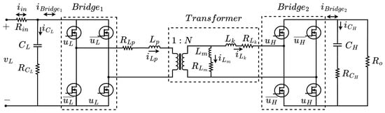
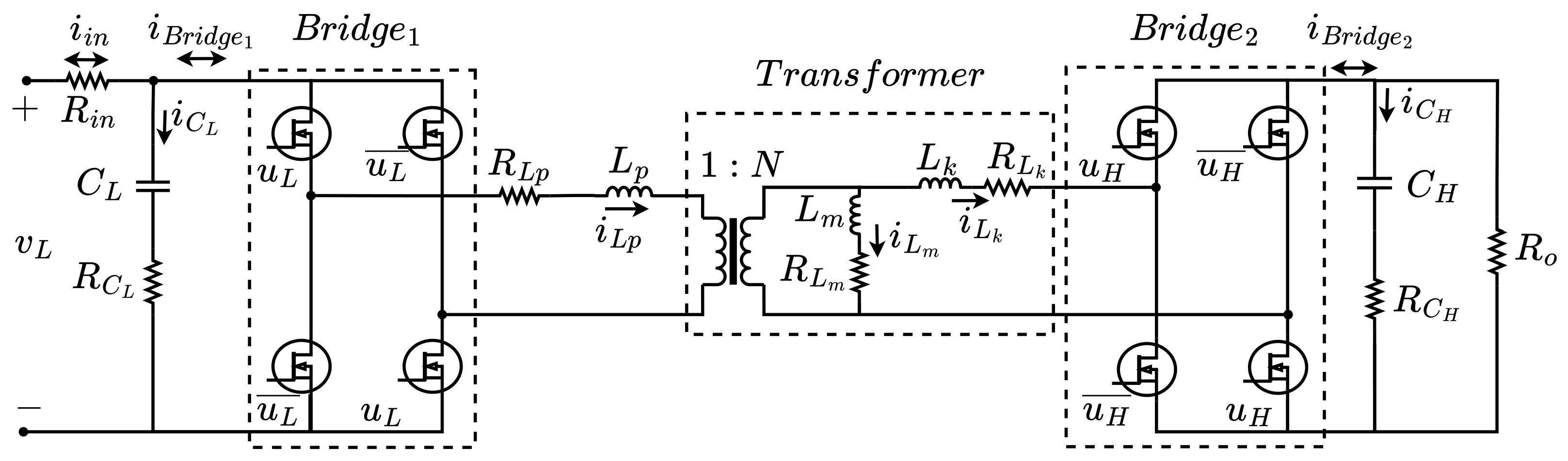
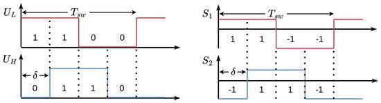
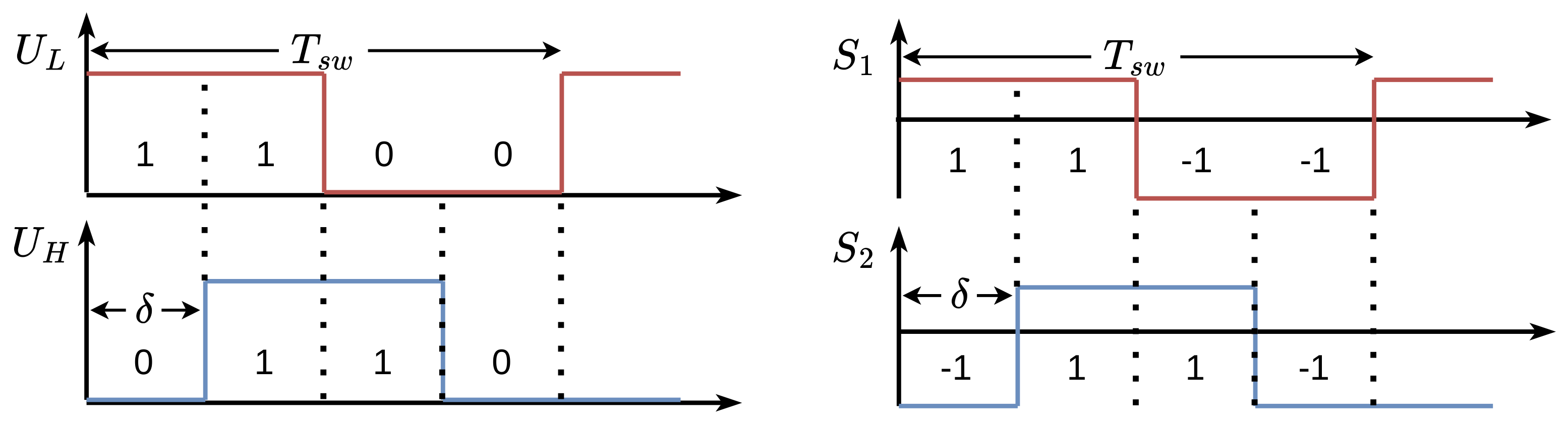
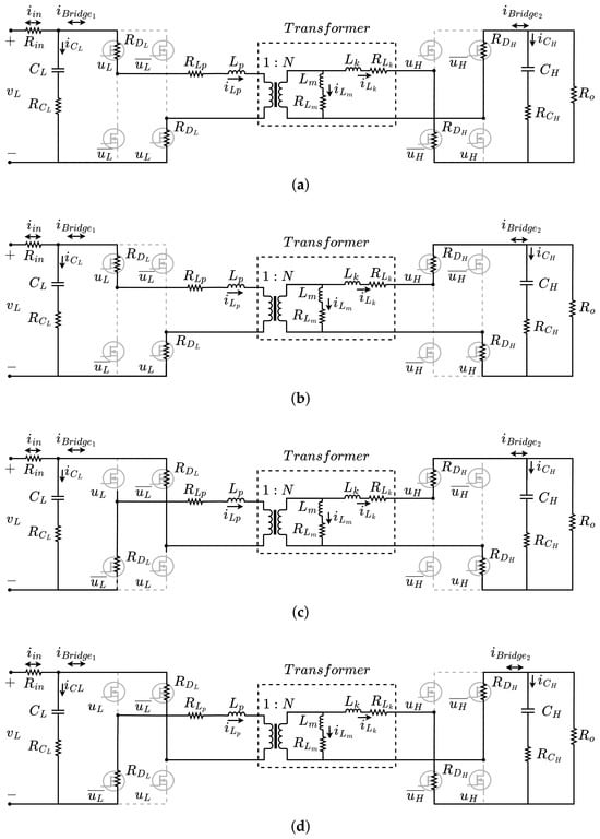
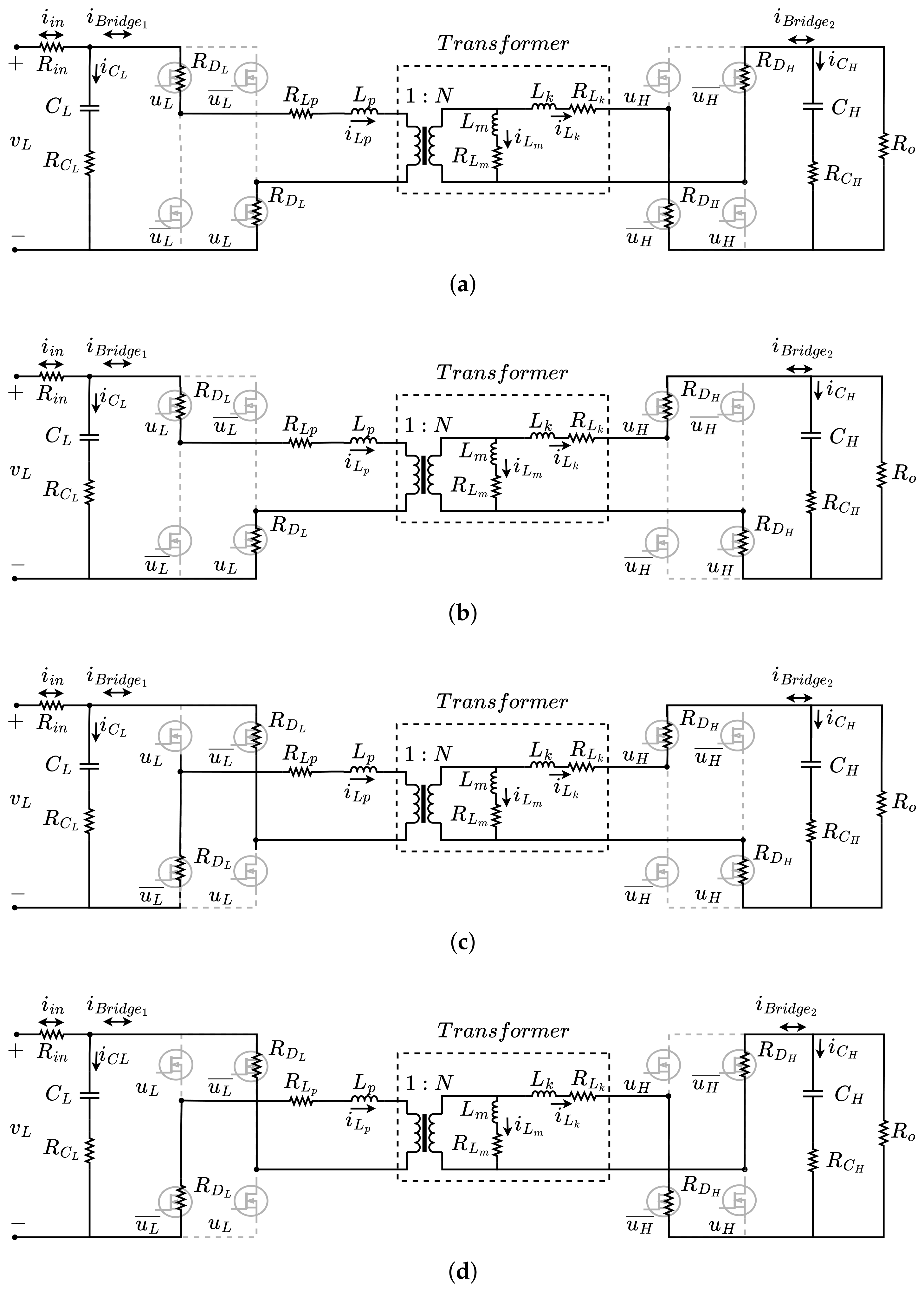
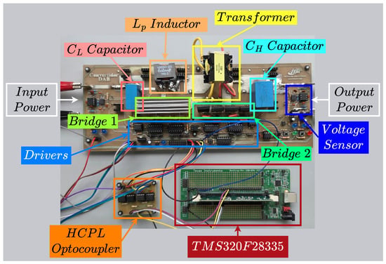
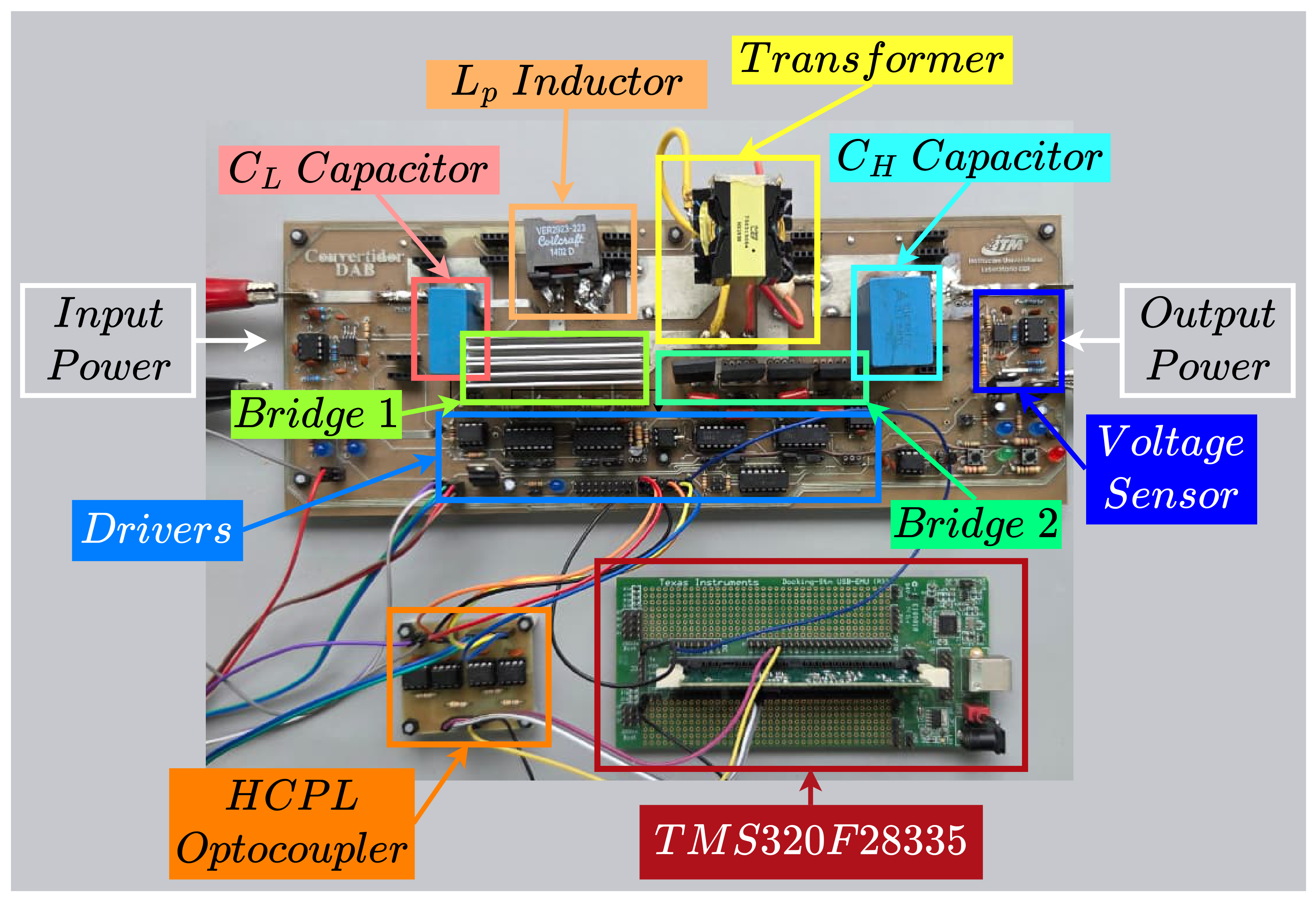
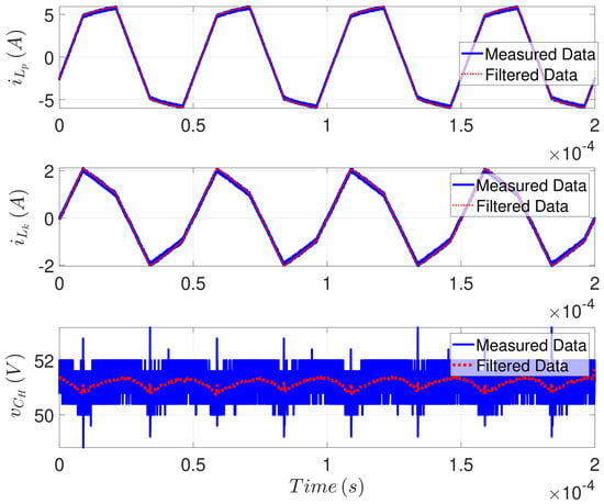
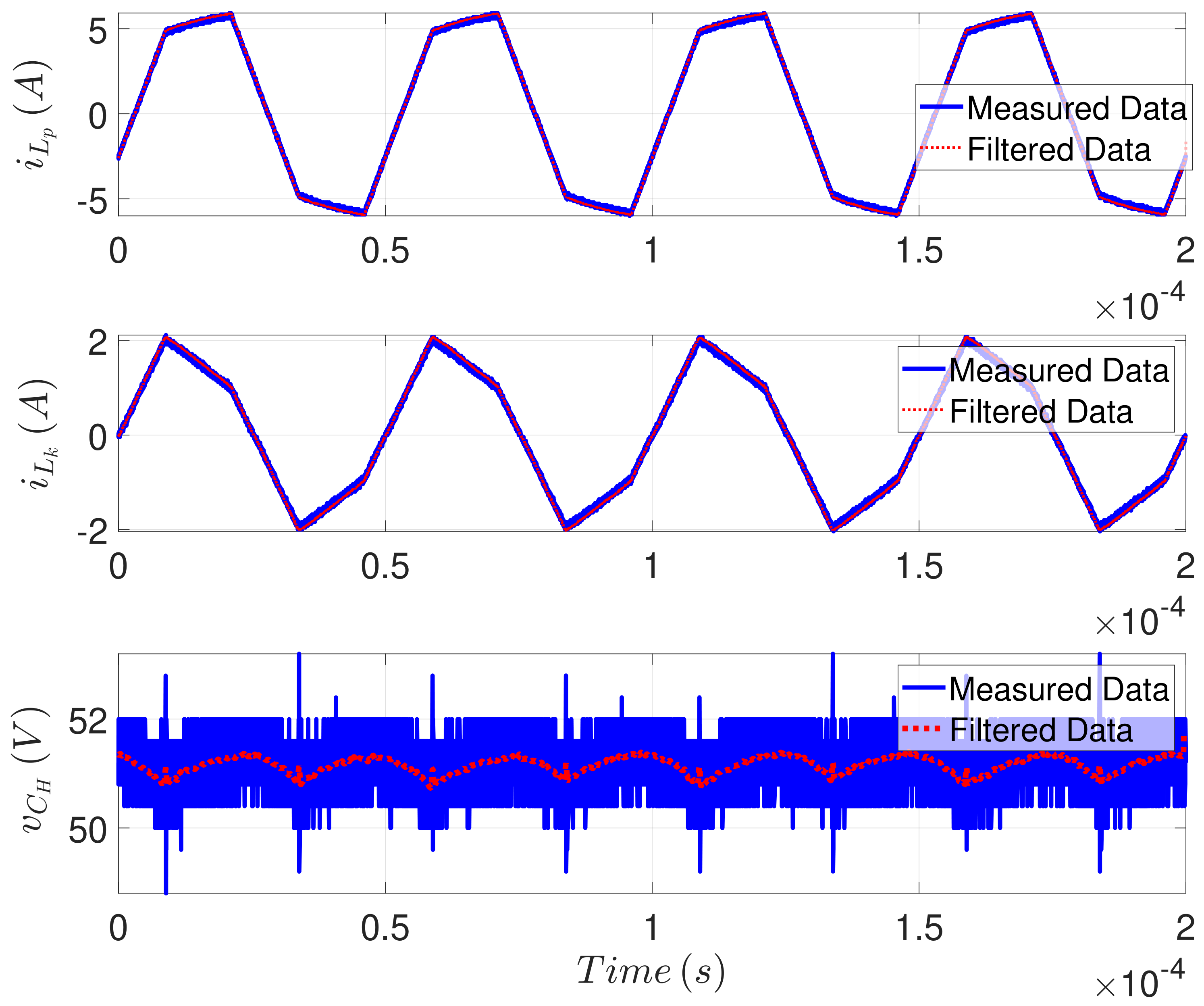
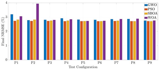
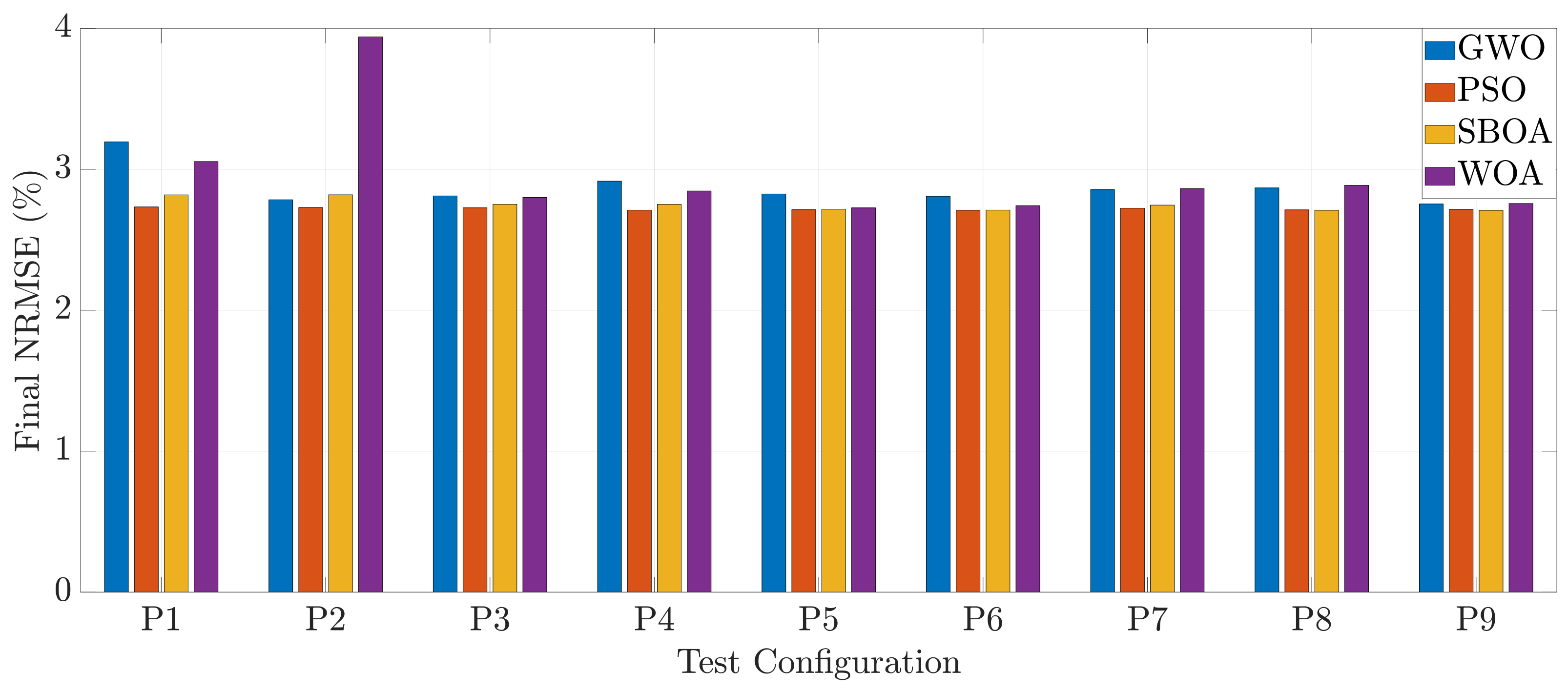
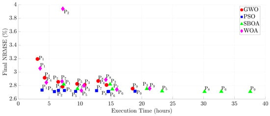
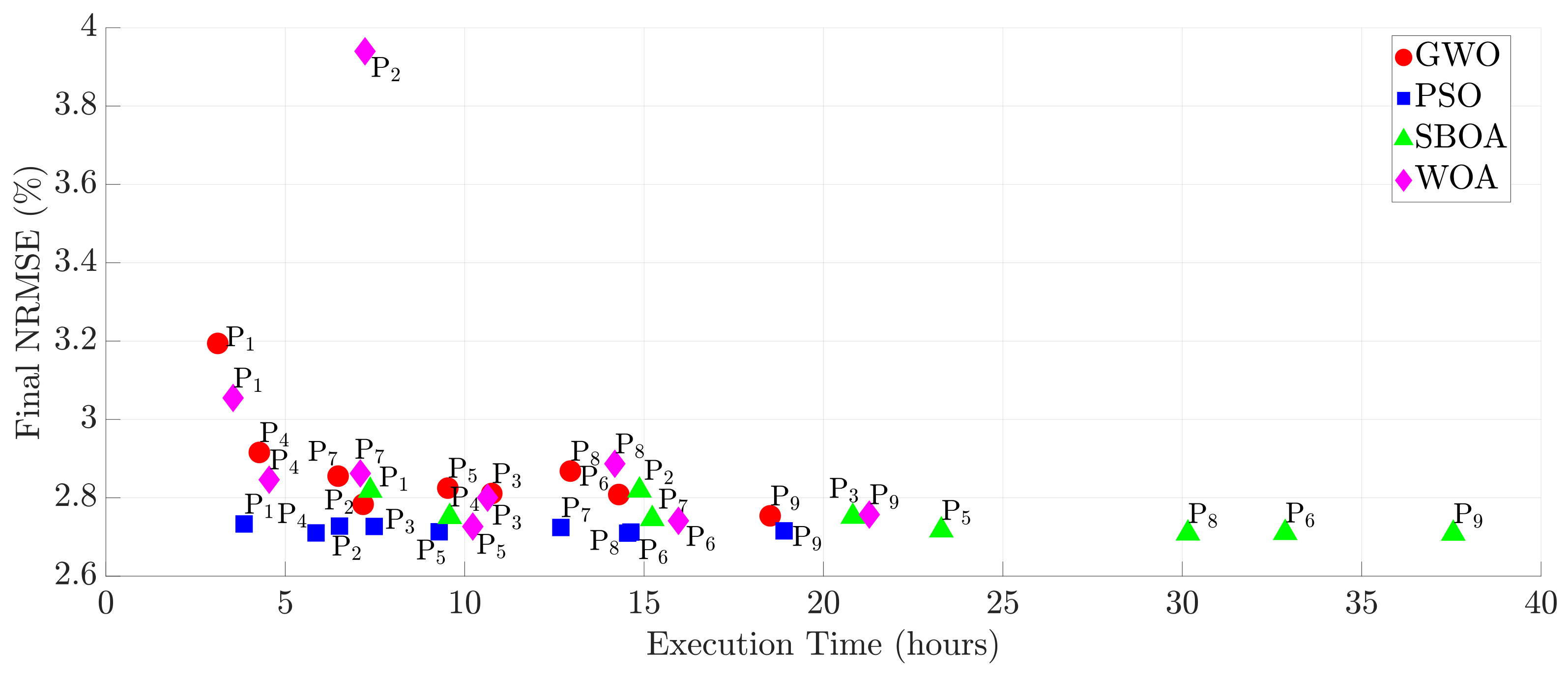
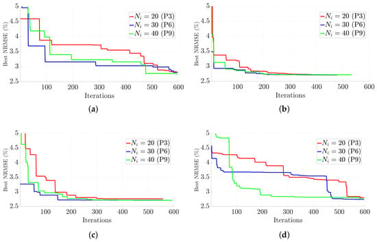
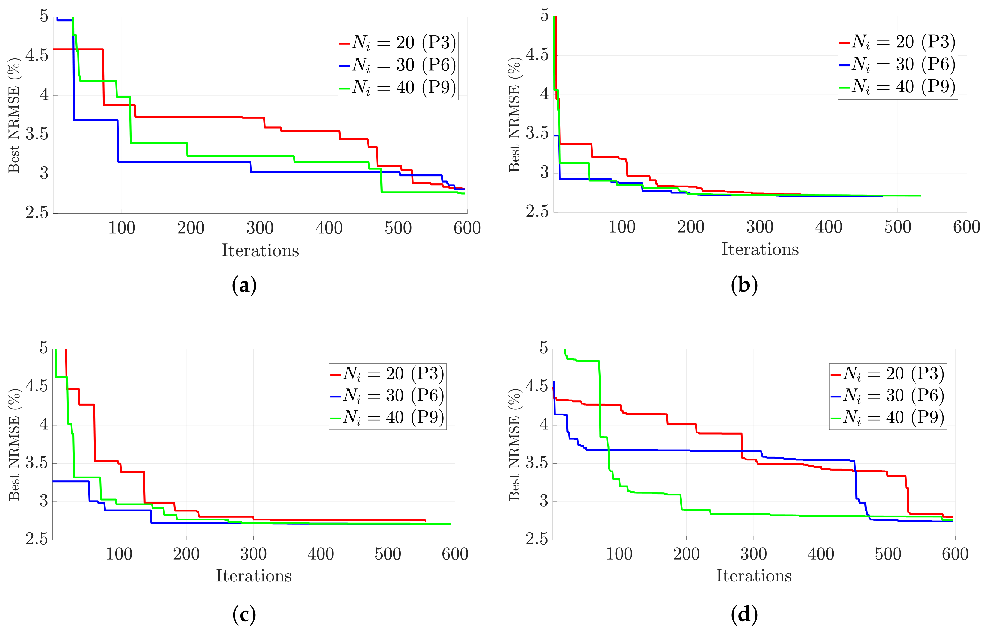
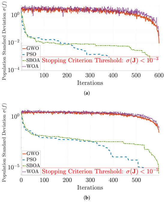
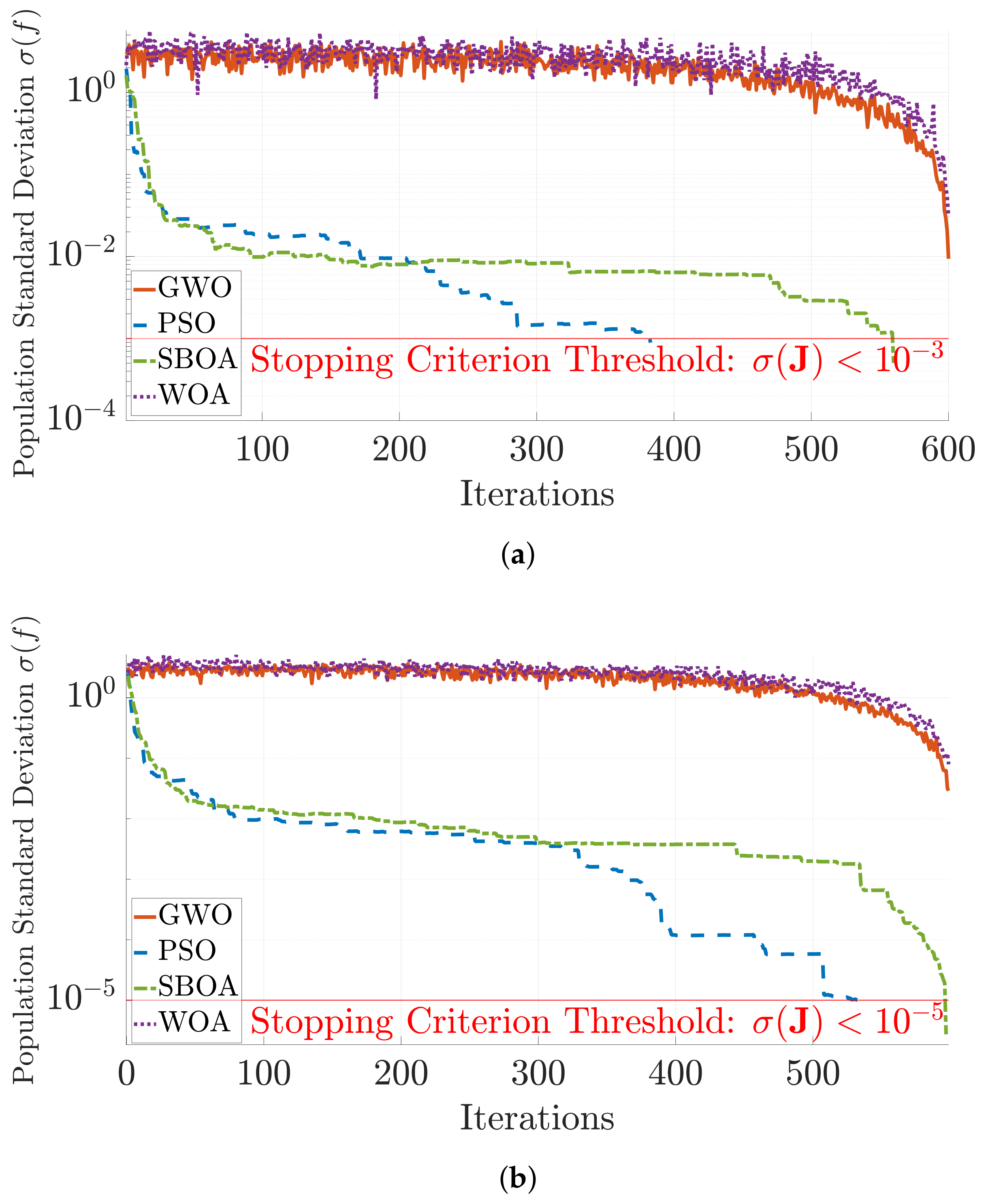
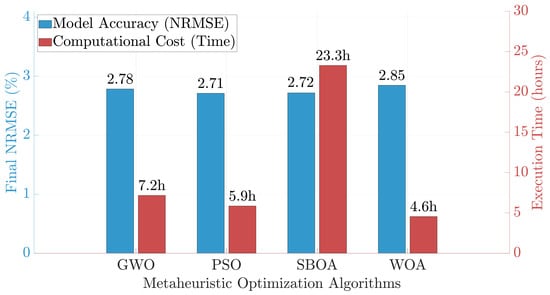
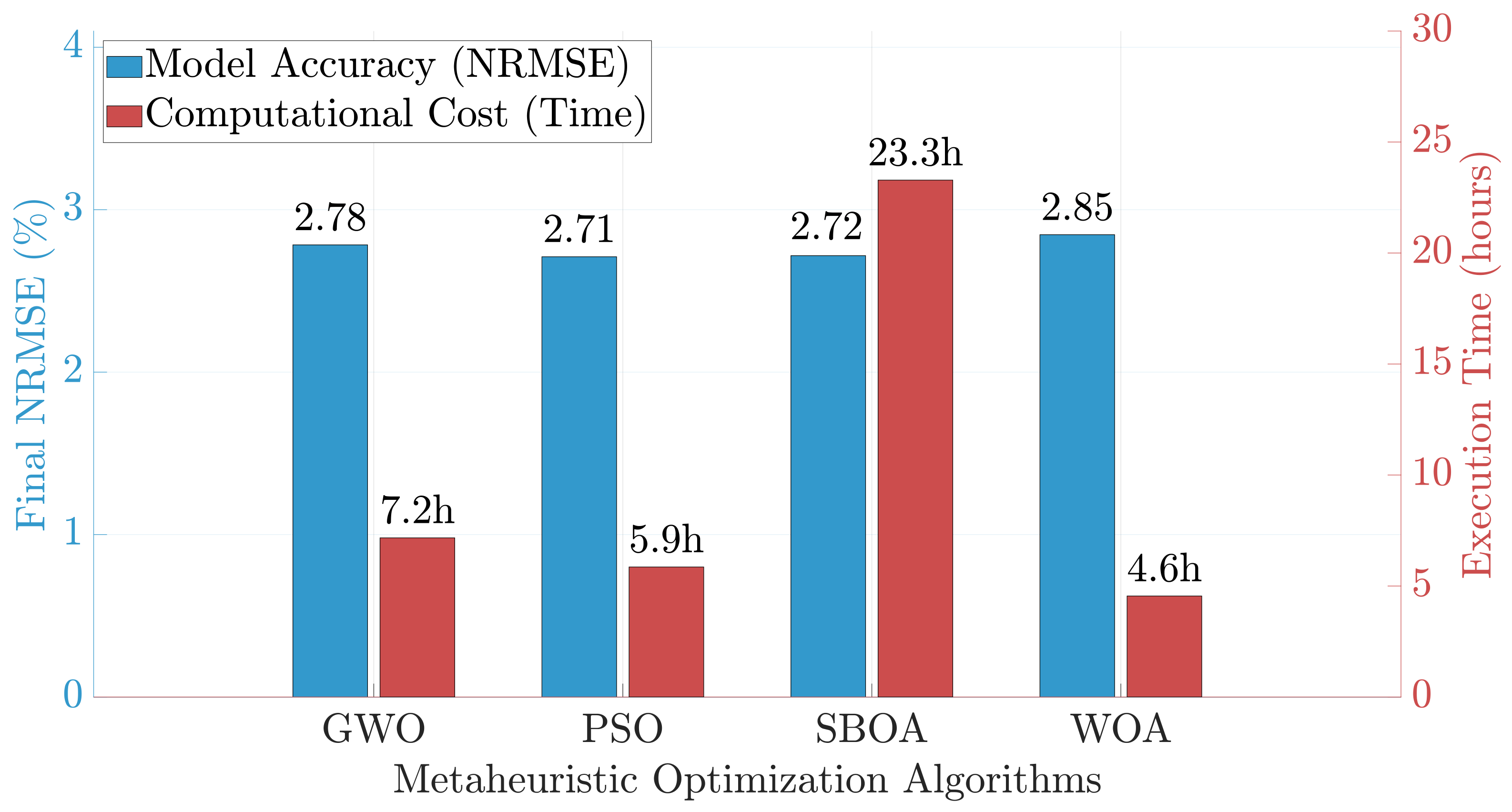
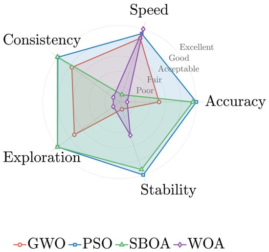
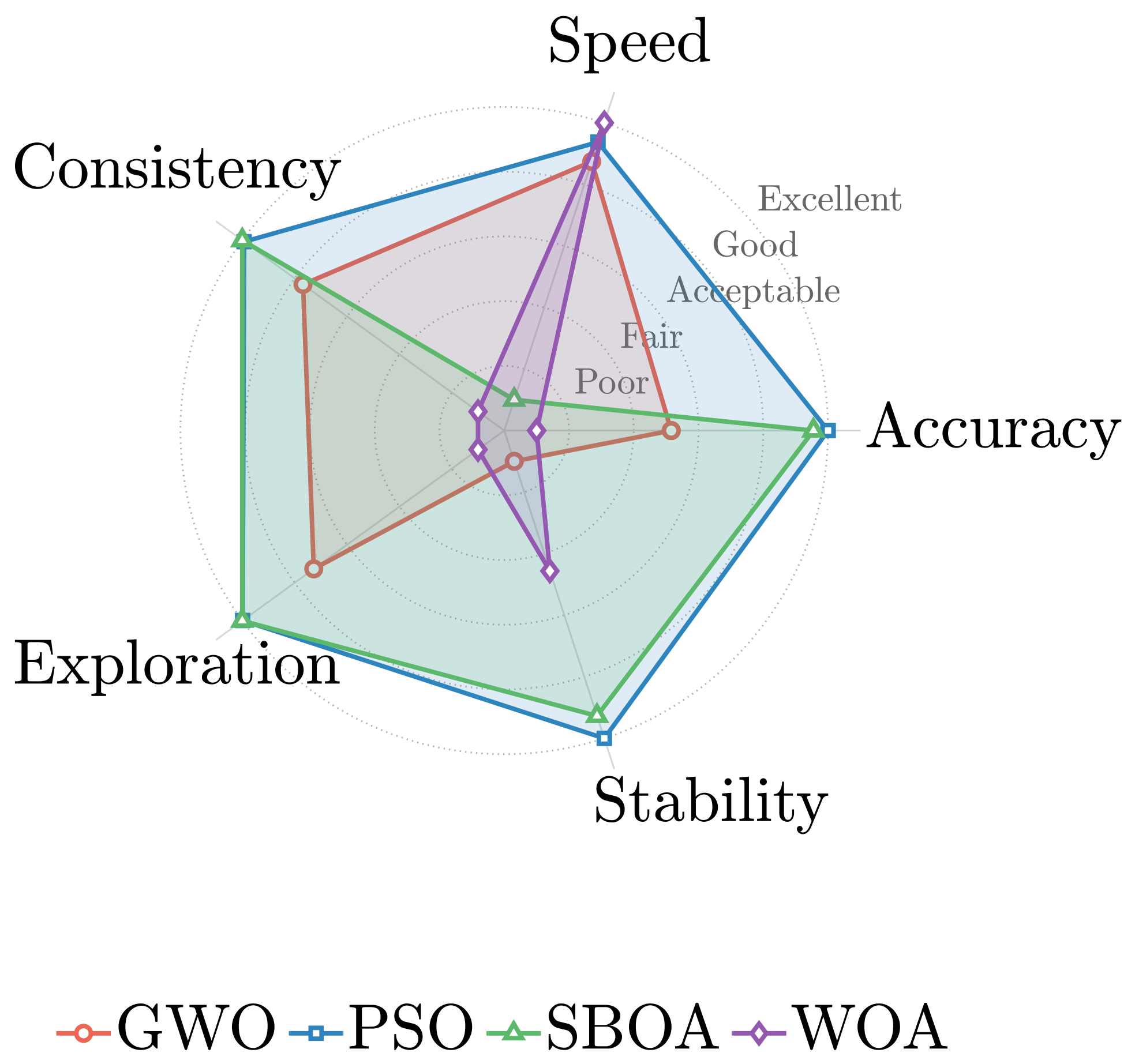
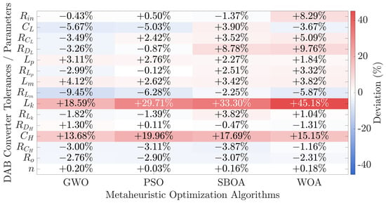
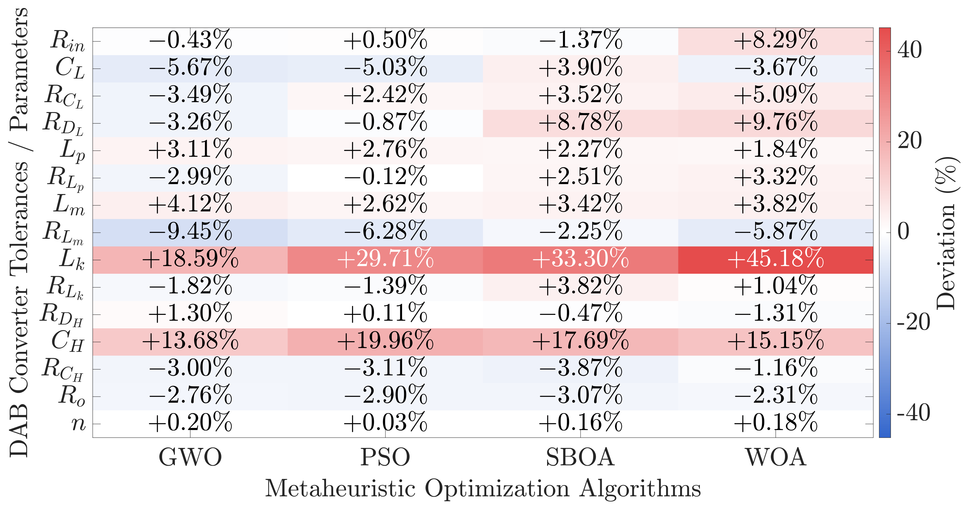
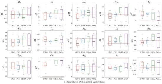
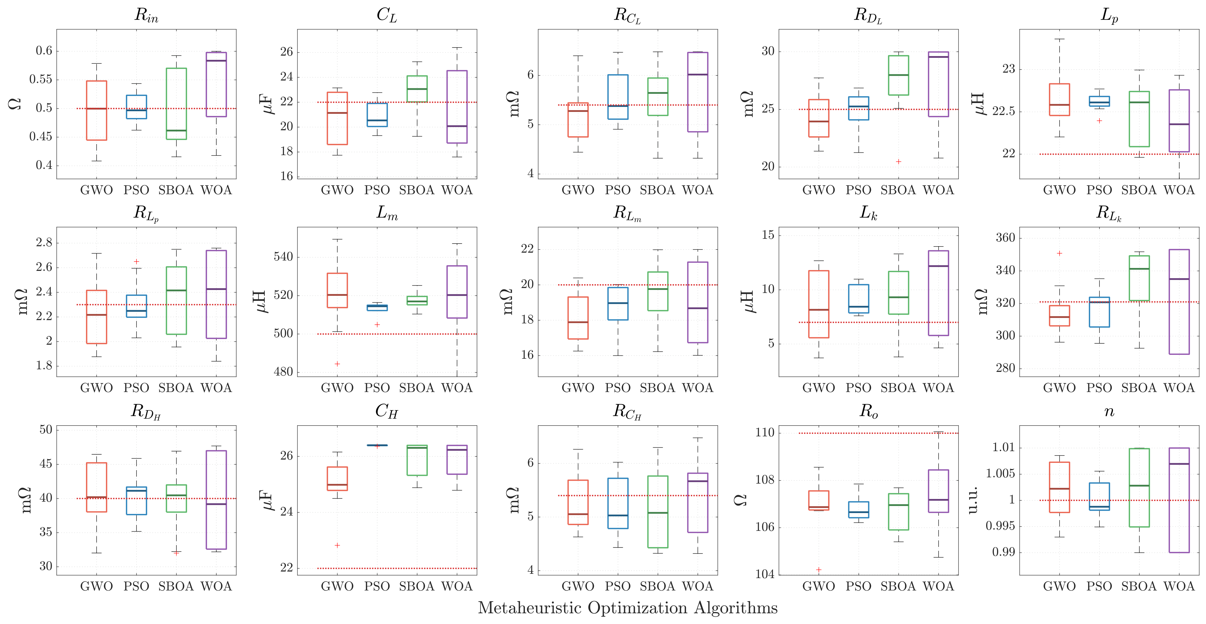
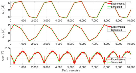
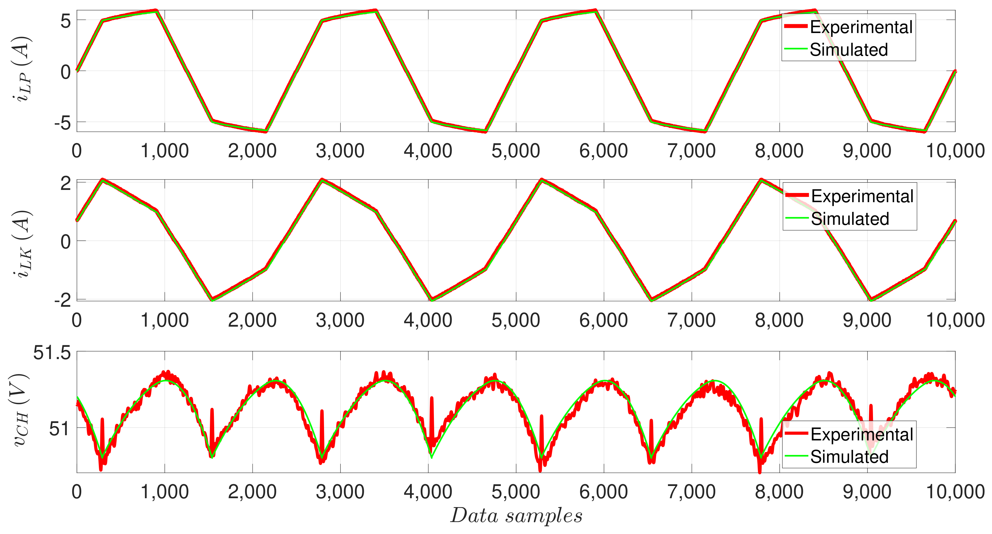
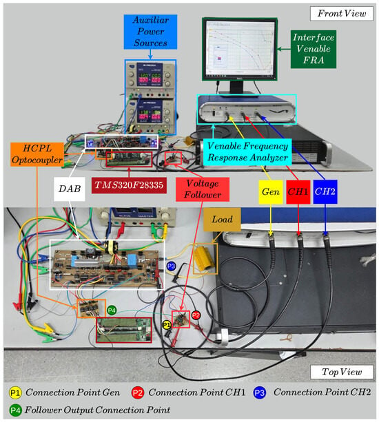
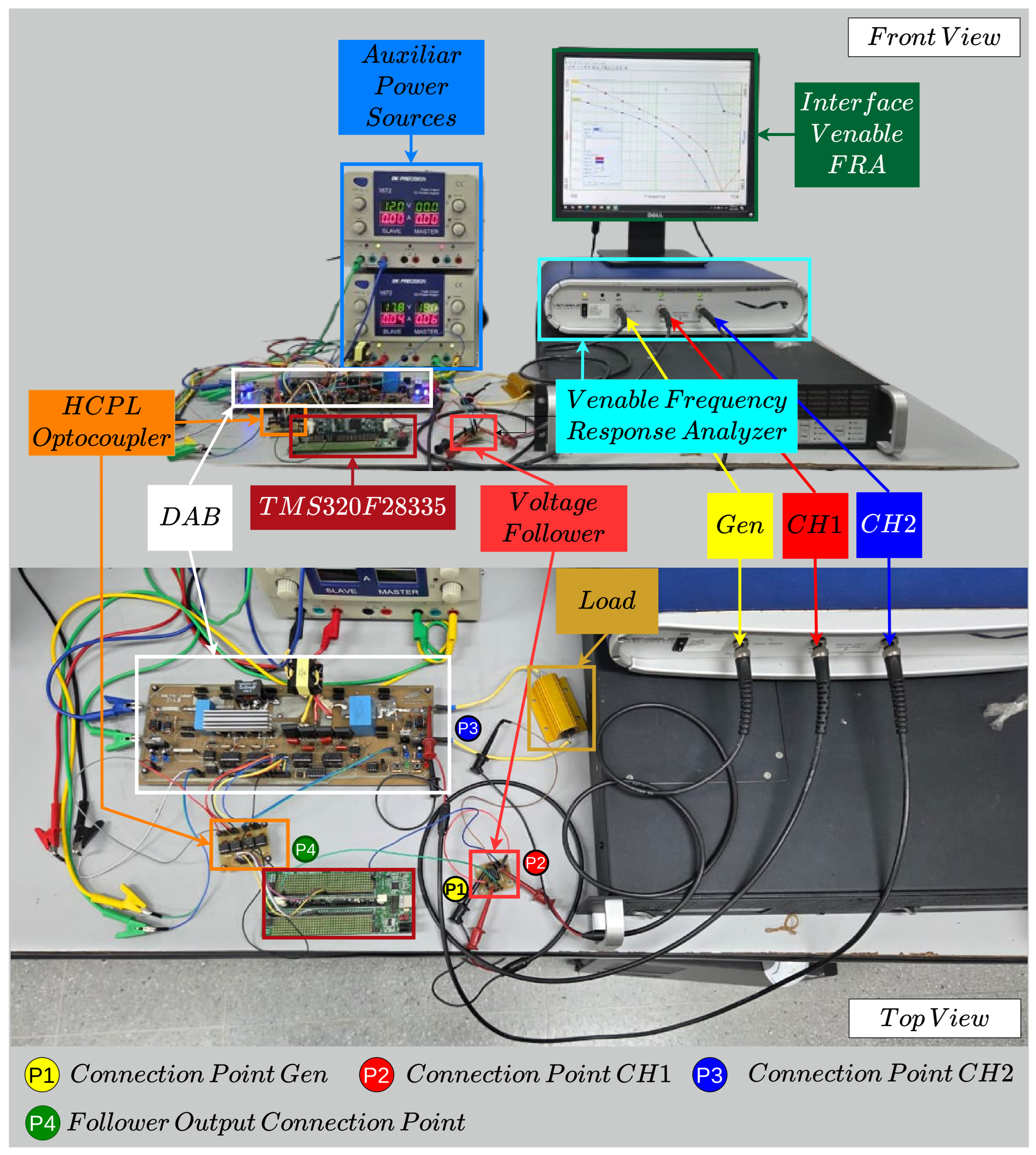
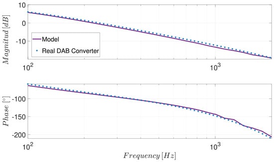
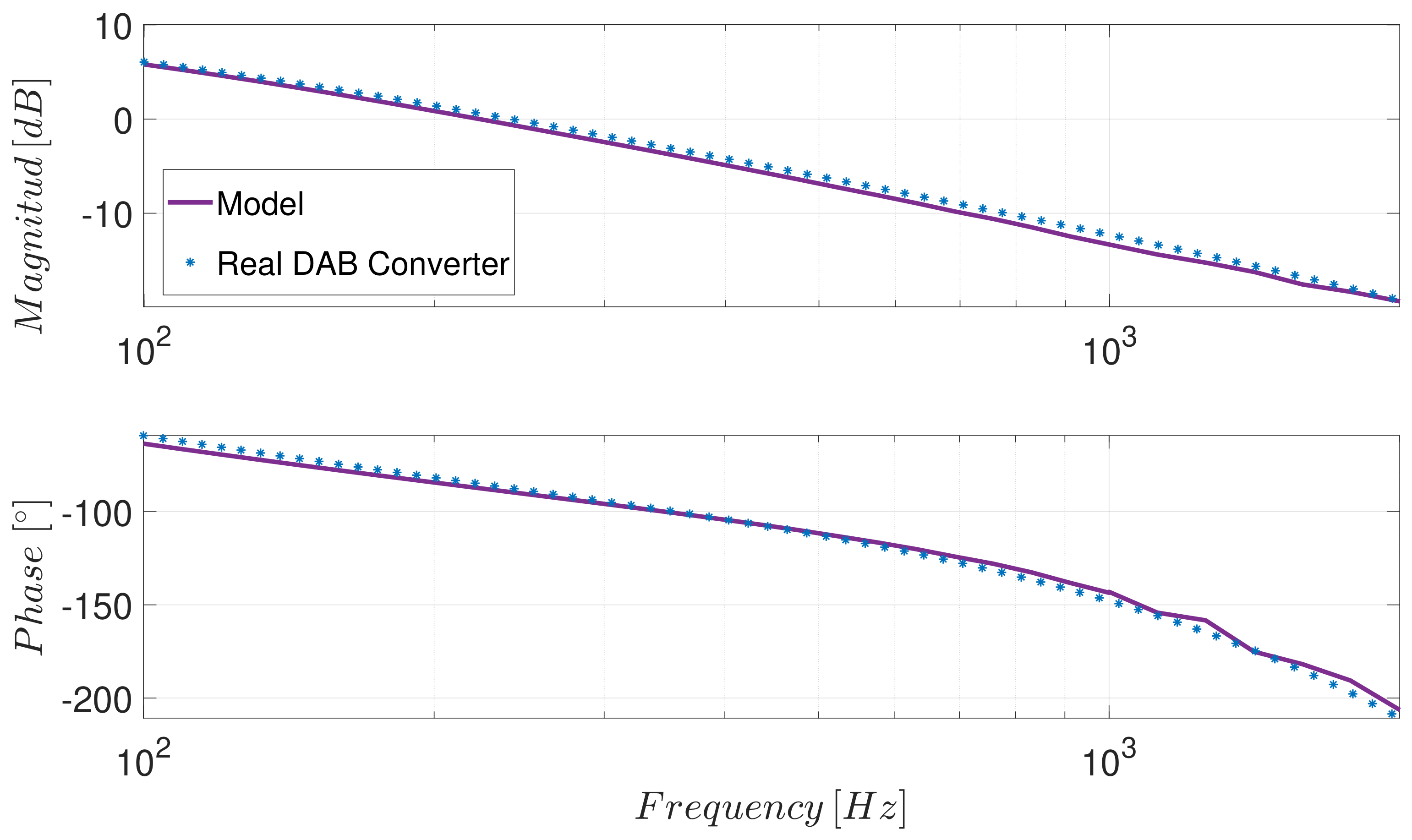
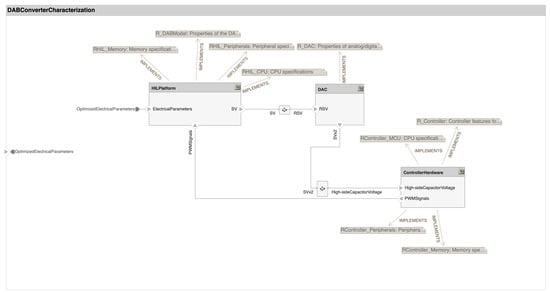
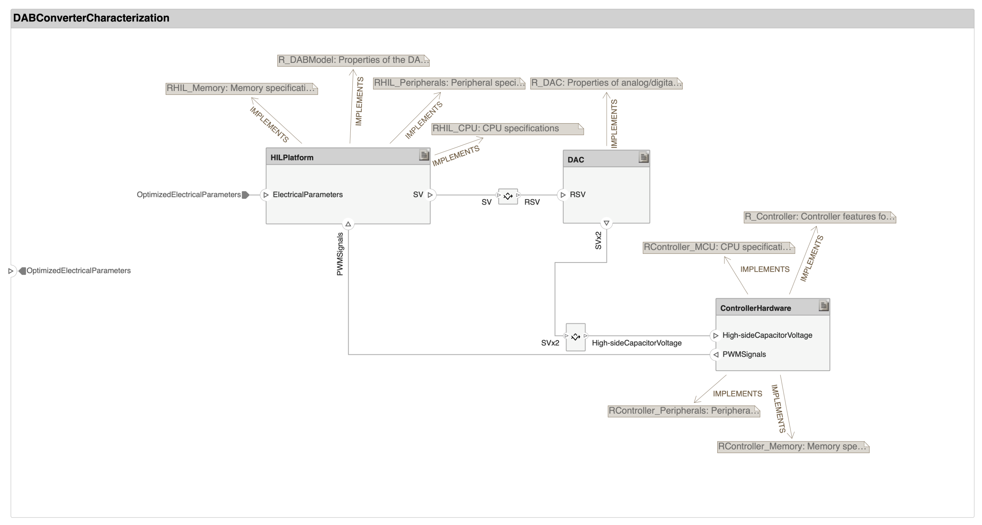
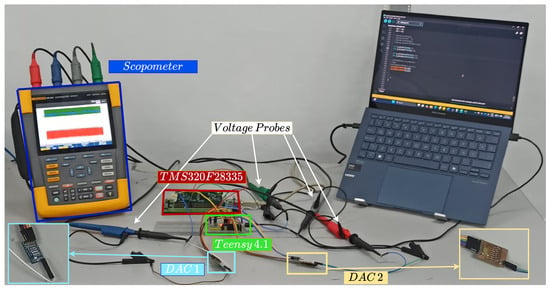
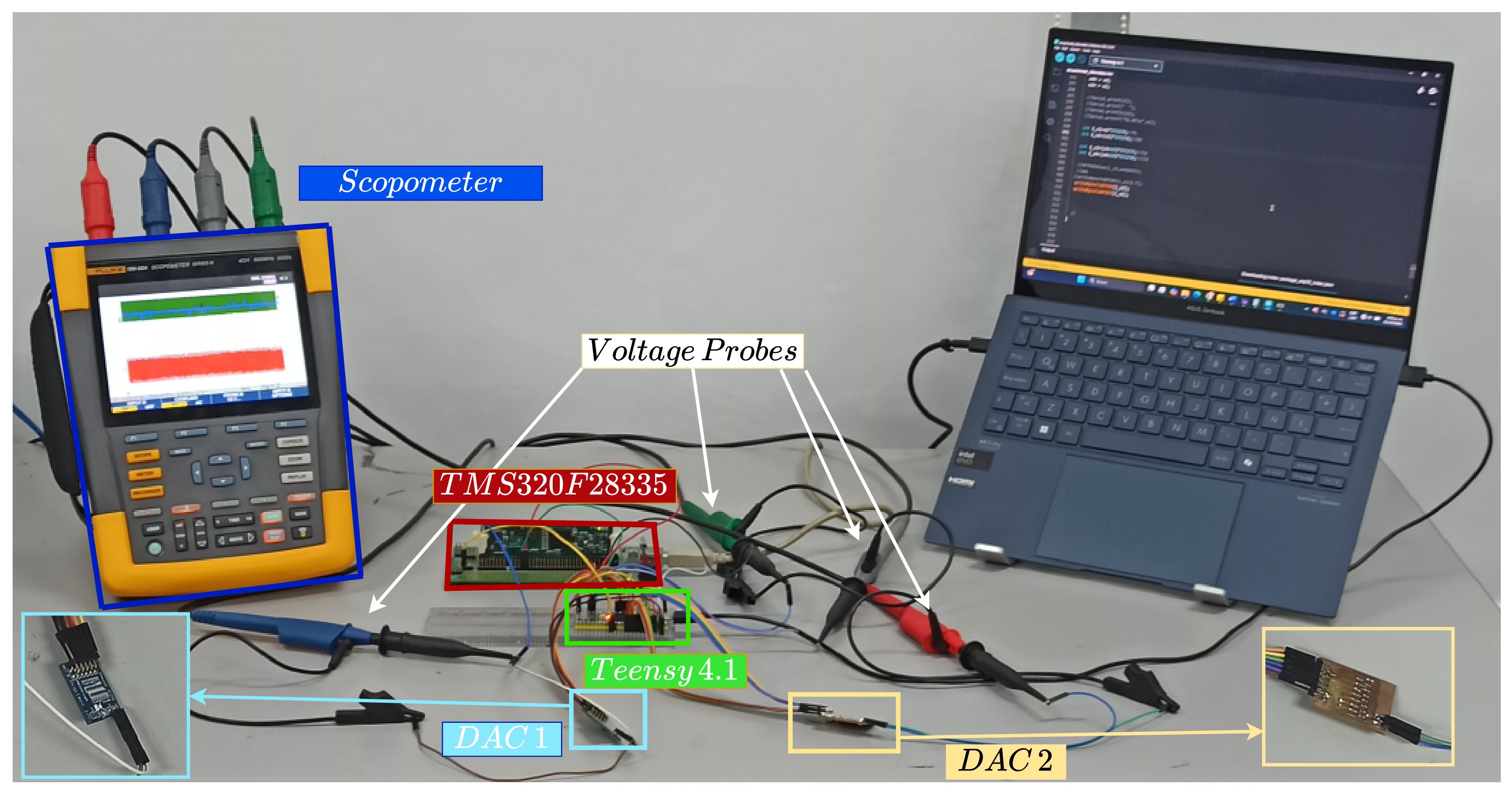
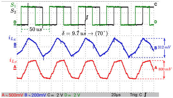
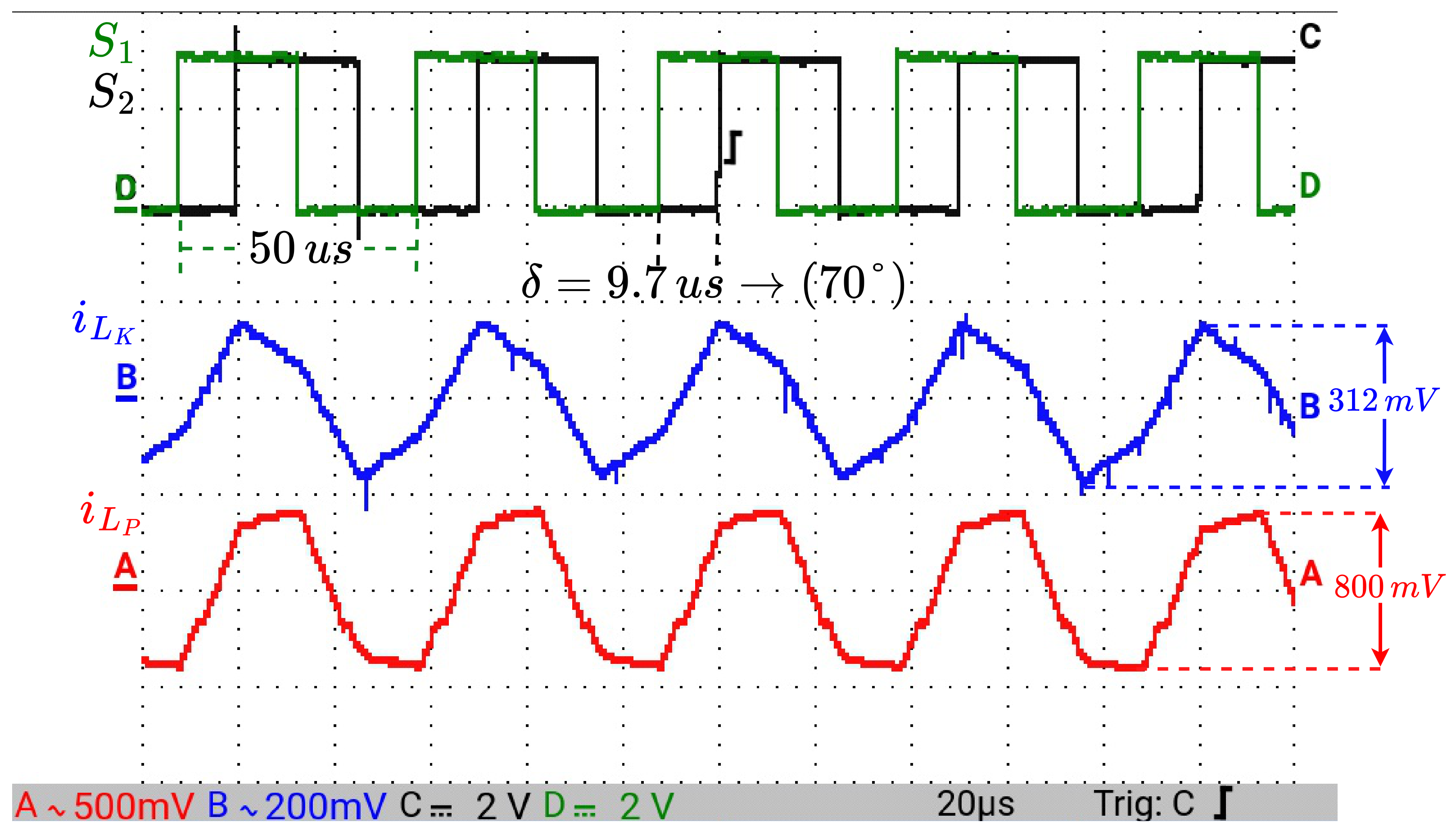
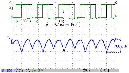
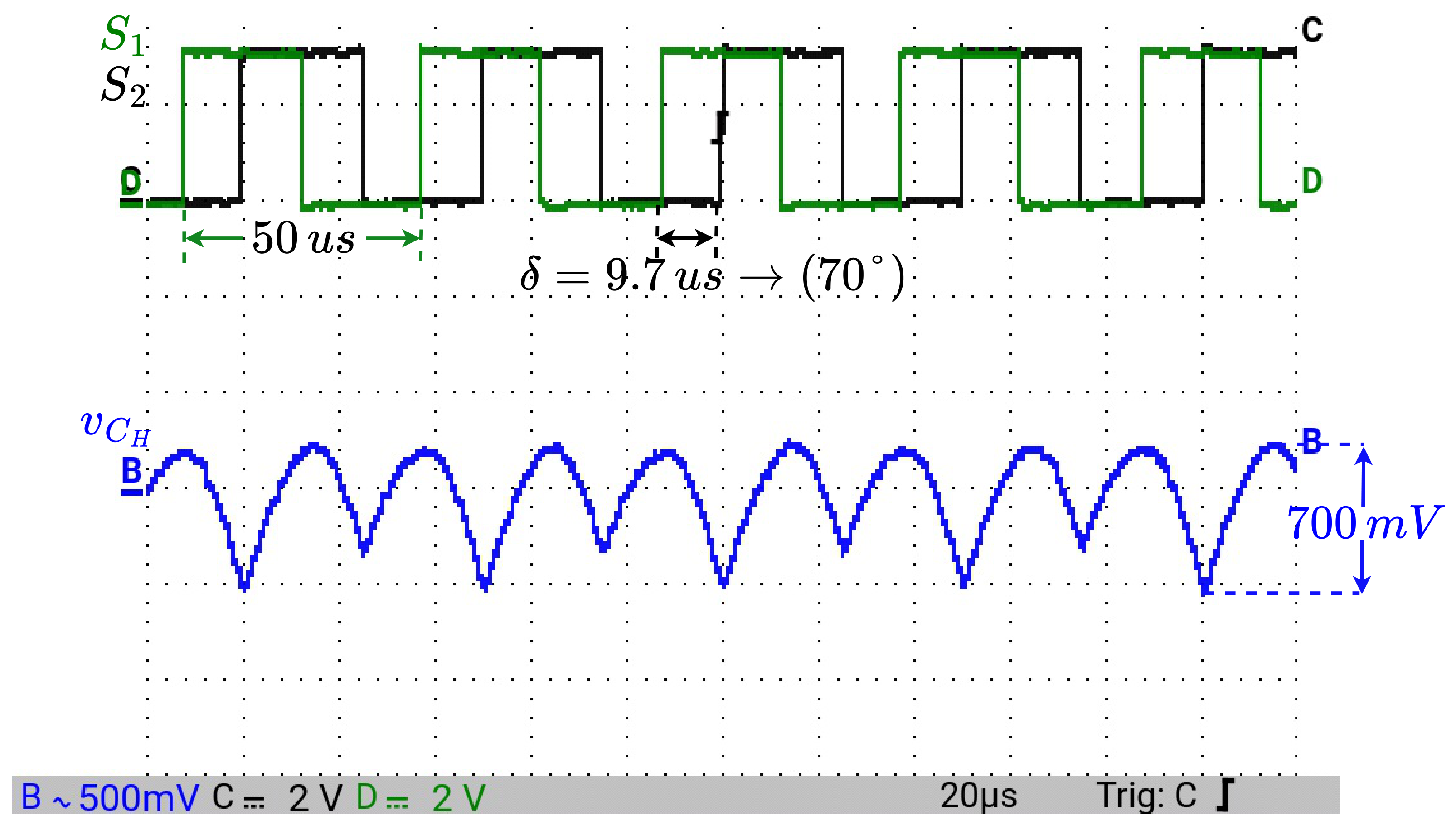
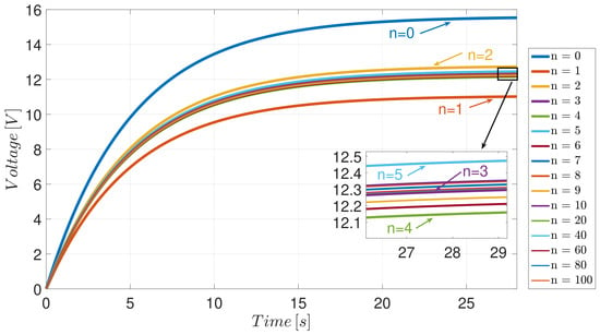
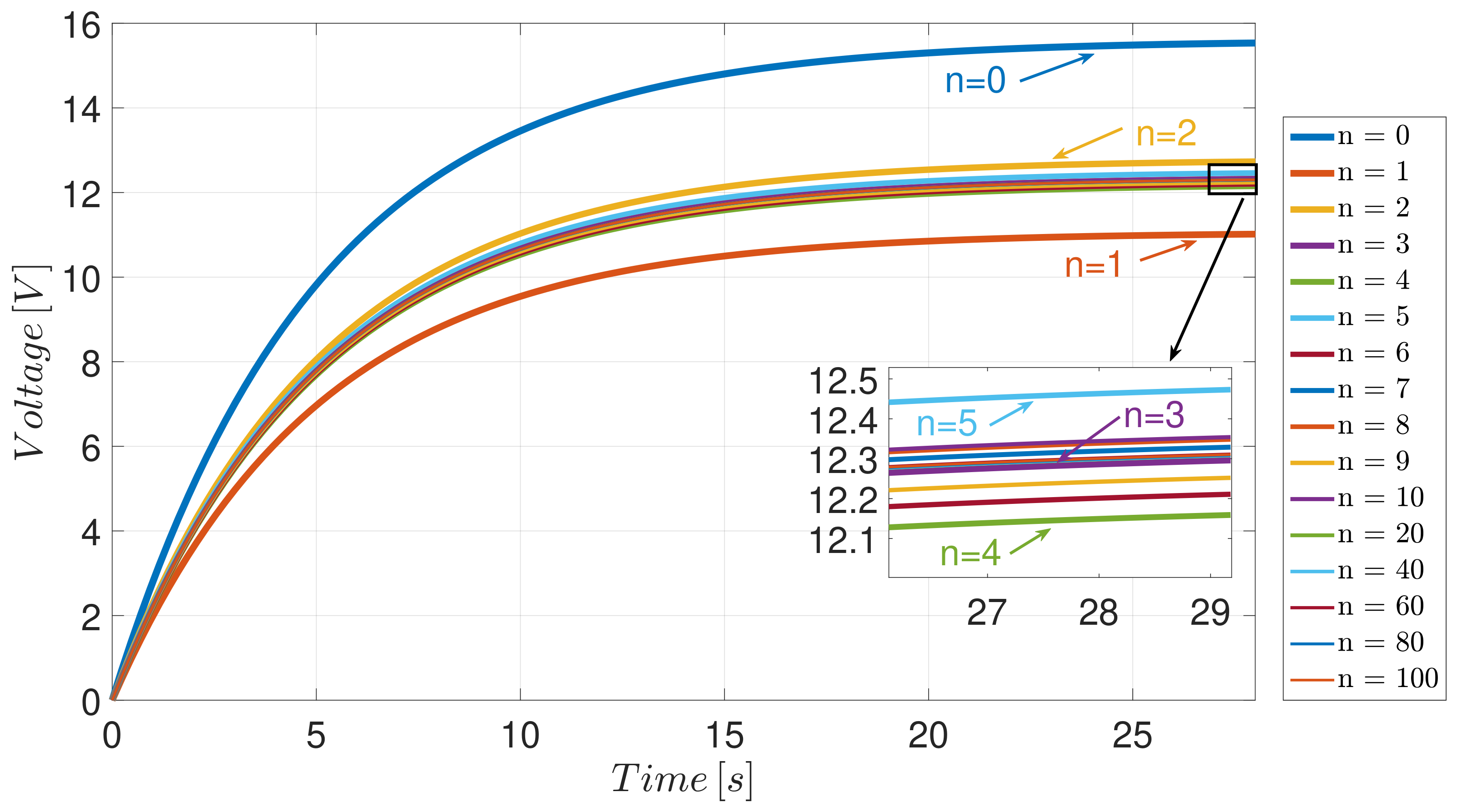
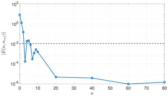
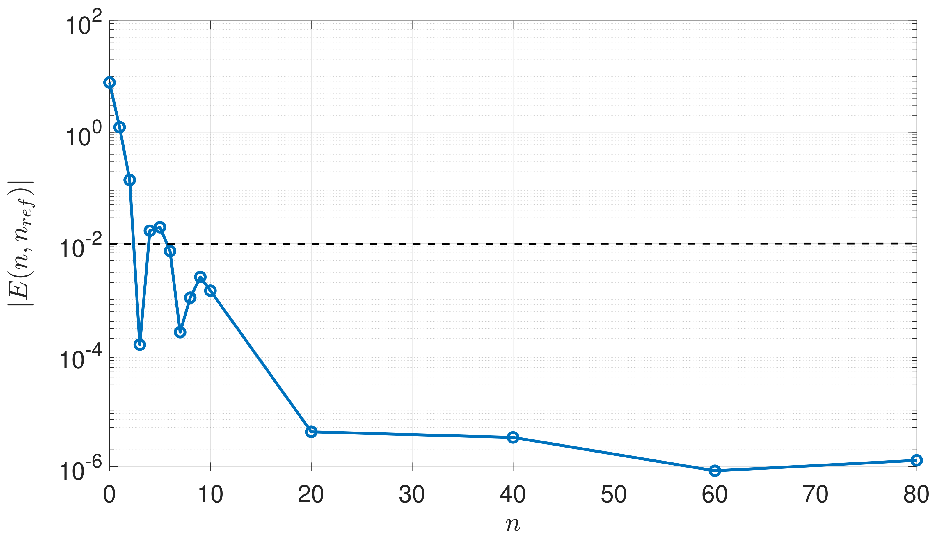
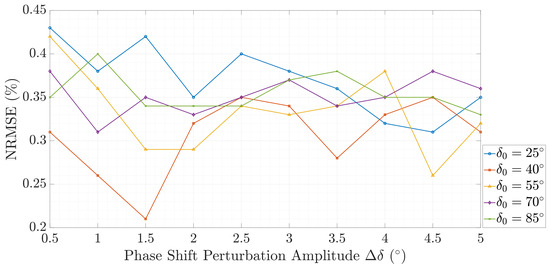
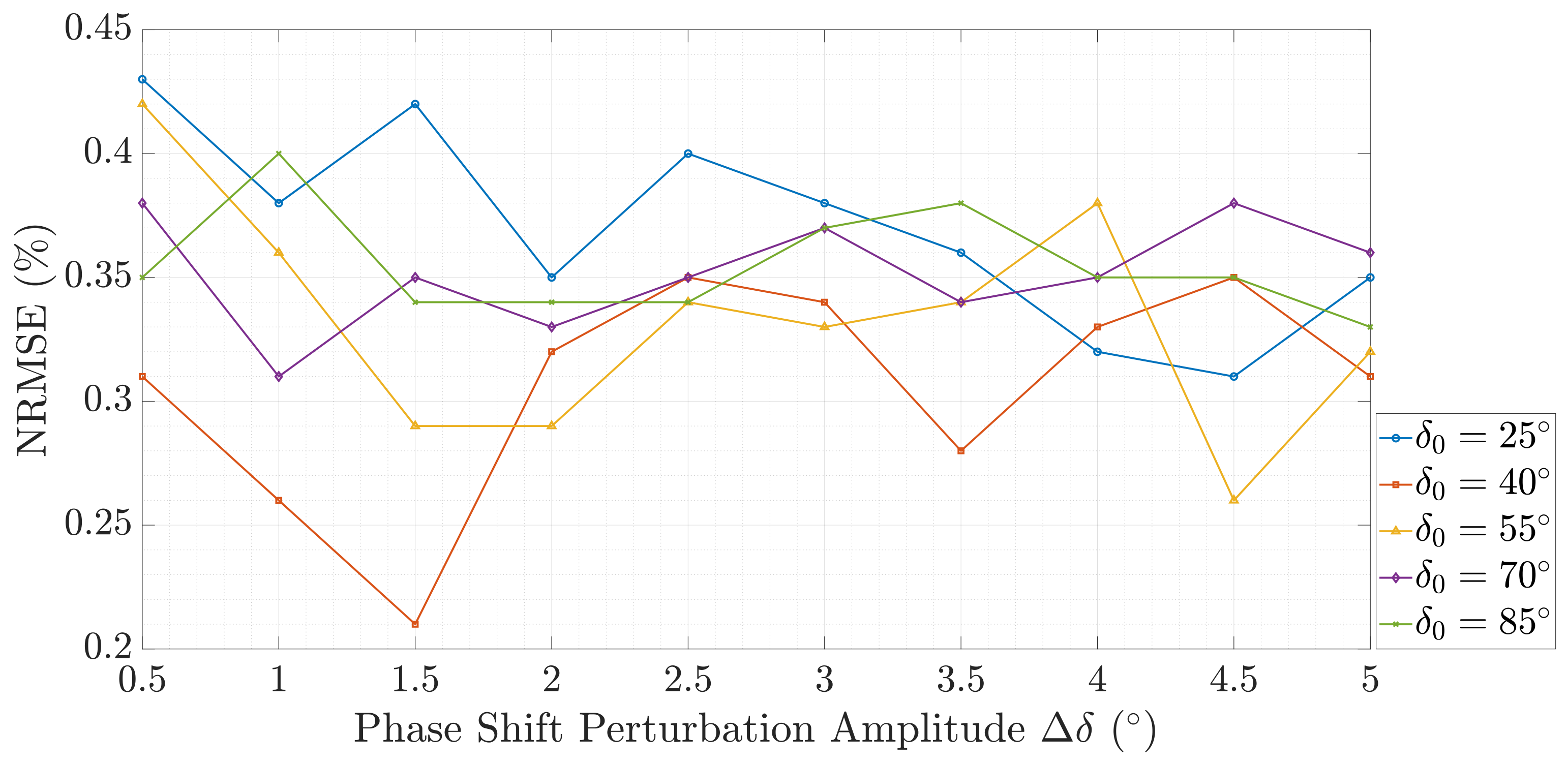
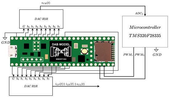
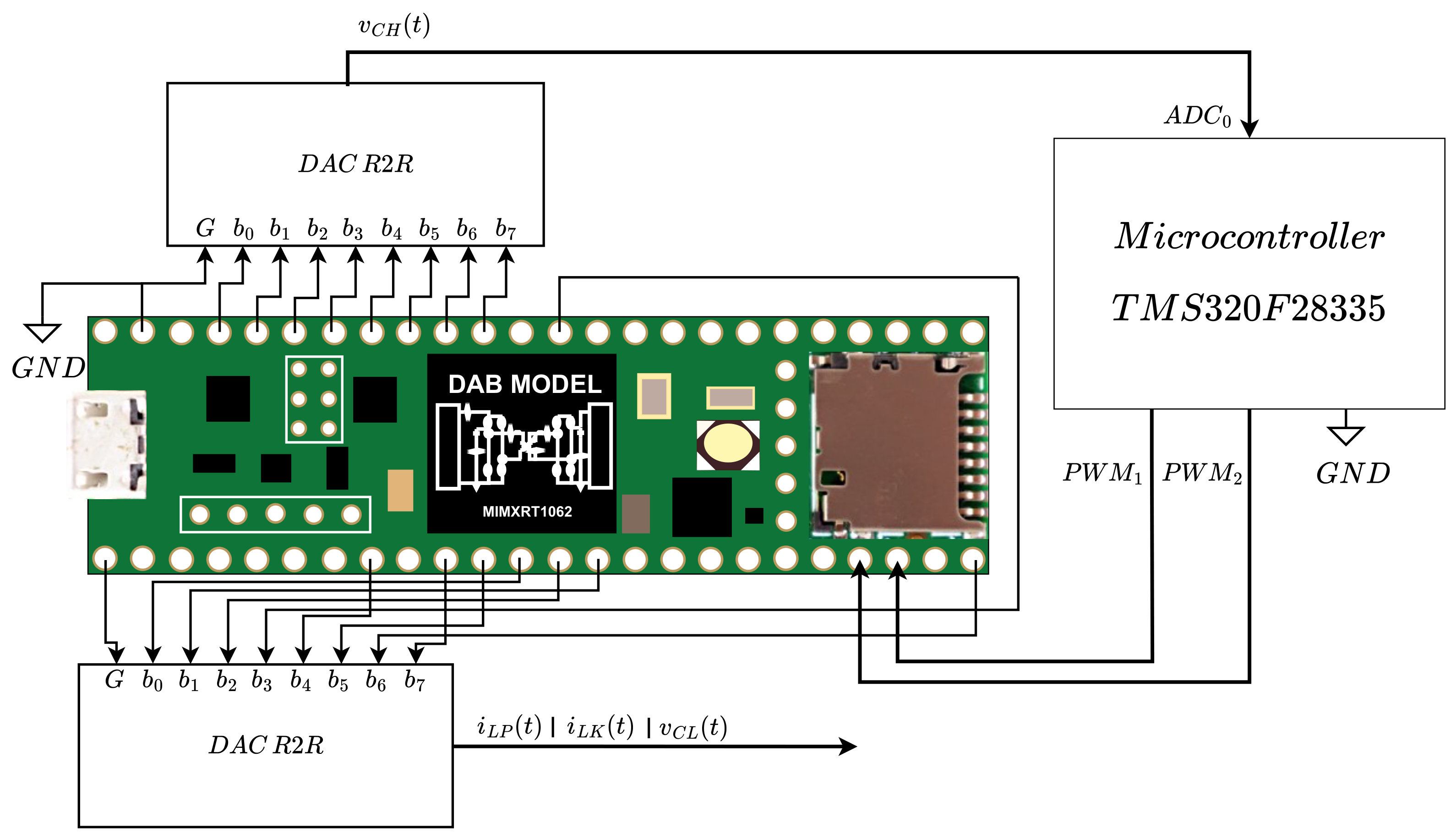
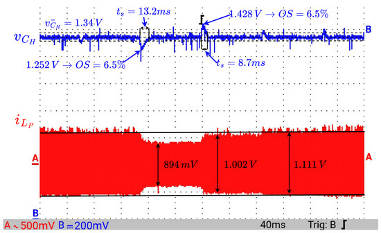
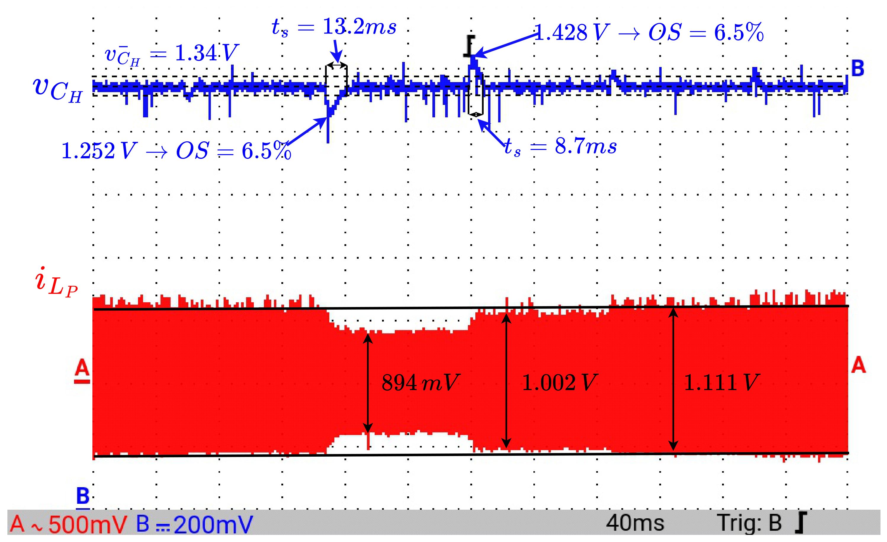
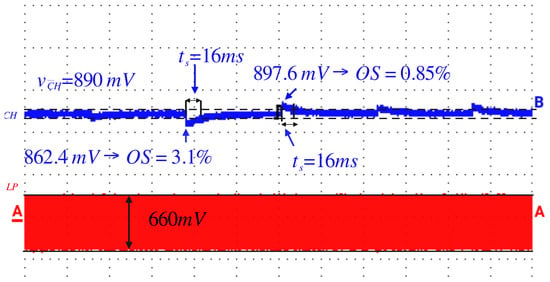
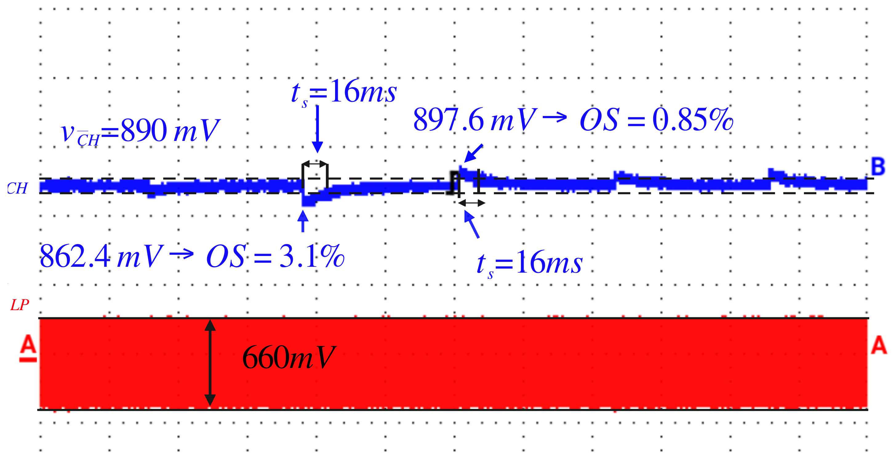
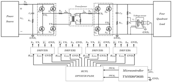
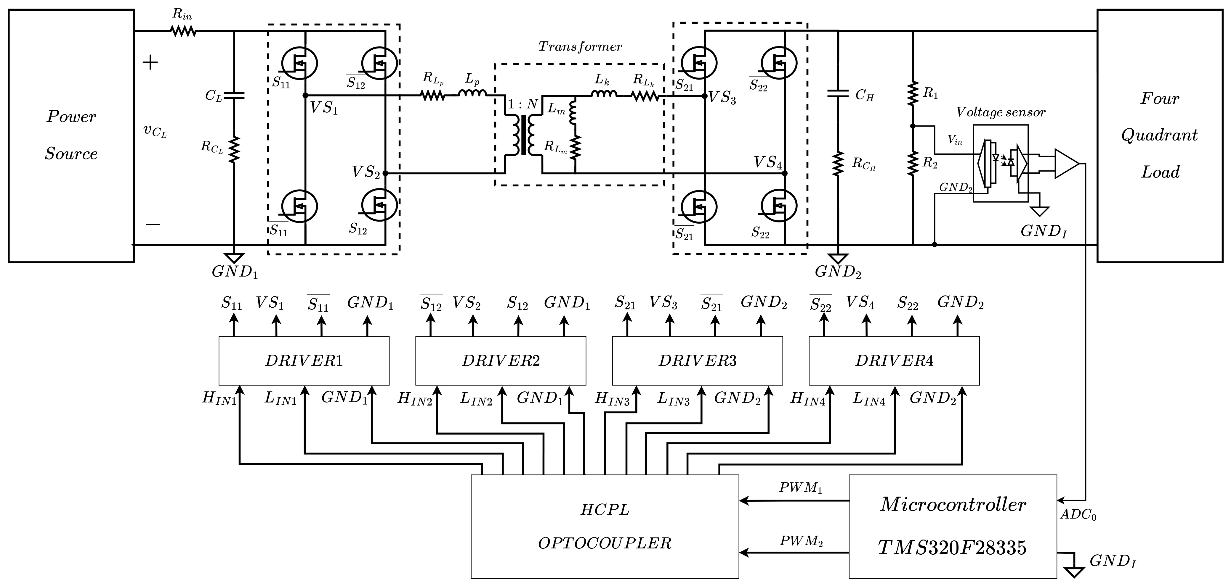
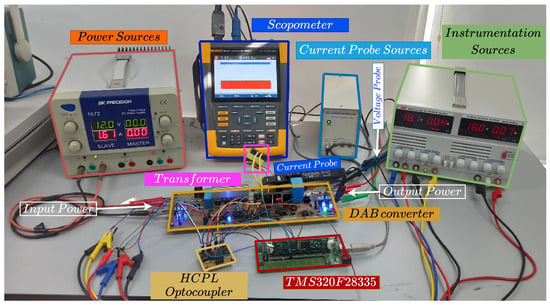
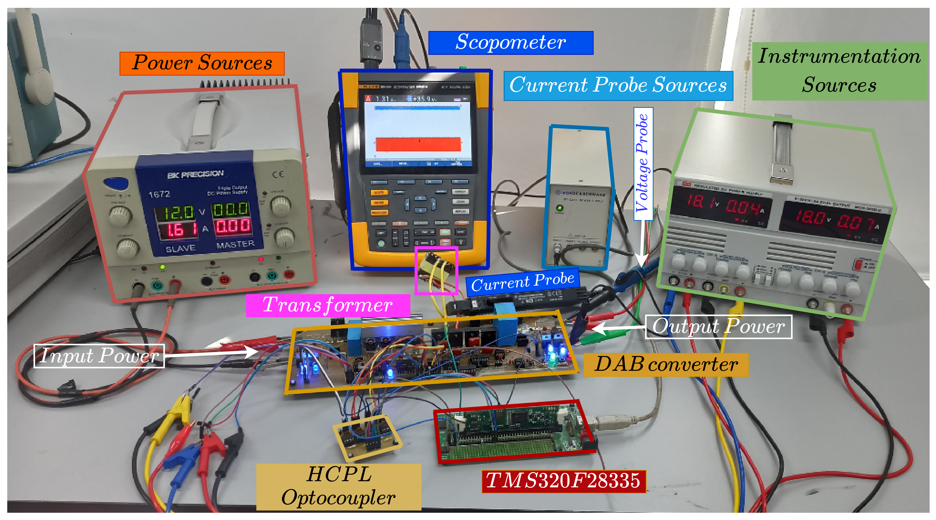
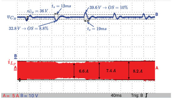
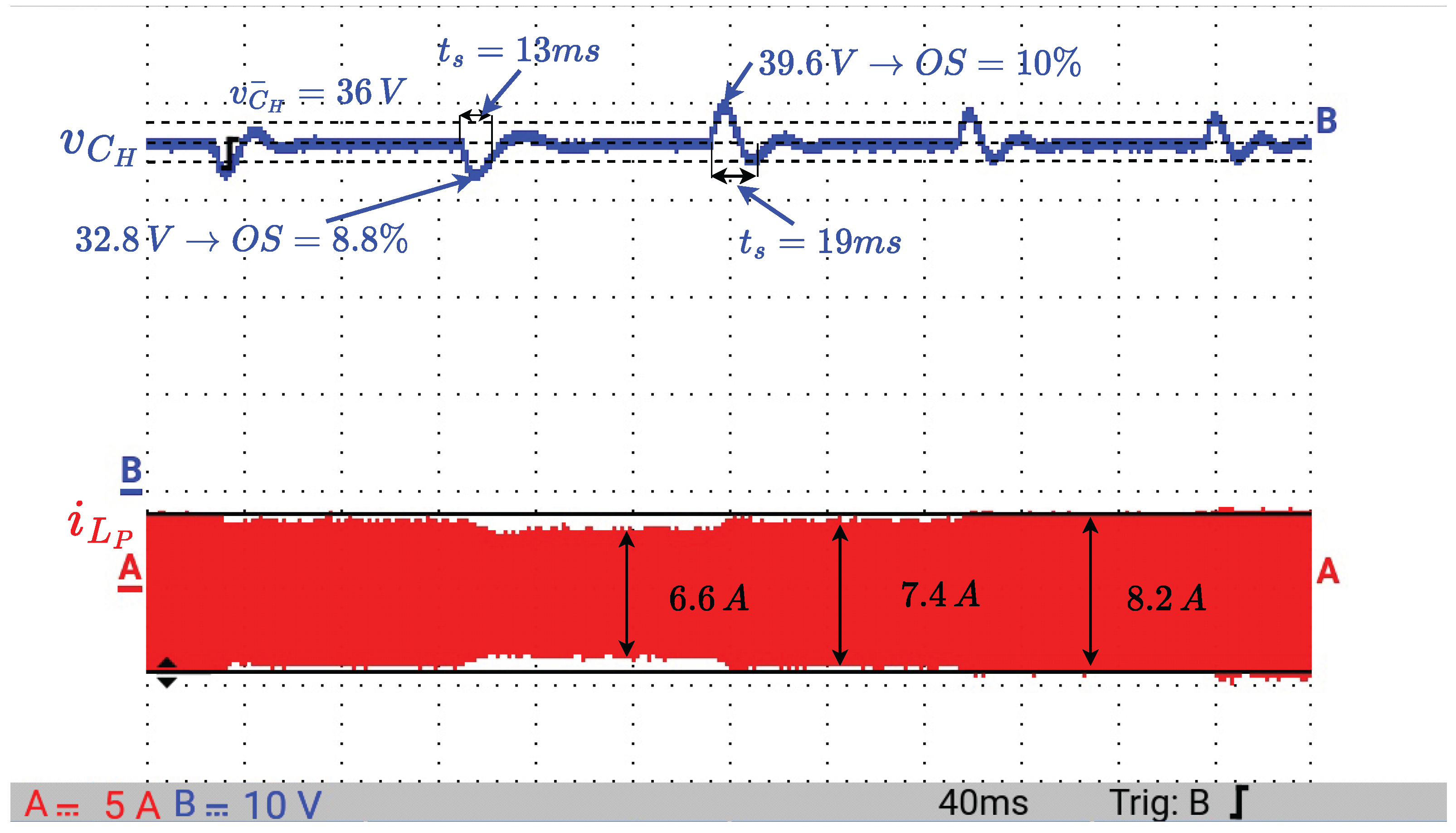

Disclaimer/Publisher’s Note: The statements, opinions and data contained in all publications are solely those of the individual author(s) and contributor(s) and not of MDPI and/or the editor(s). MDPI and/or the editor(s) disclaim responsibility for any injury to people or property resulting from any ideas, methods, instructions or products referred to in the content. |
© 2026 by the authors. Licensee MDPI, Basel, Switzerland. This article is an open access article distributed under the terms and conditions of the Creative Commons Attribution (CC BY) license.