


Abstract
This paper presents the design and experimental validation of a passive I/Q downconversion subsystem for X-band applications, with emphasis on maritime radar operation. The proposed architecture combines passive RF and LO distribution networks with a single-balanced passive mixer, enabling accurate quadrature signal generation without relying on active correction mechanisms. The subsystem maintains controlled amplitude and phase balance across the operating band, directly supporting effective image suppression. Experimental results demonstrate image rejection ratios exceeding 30 dB. The mixer stage exhibits a conversion loss of approximately 6 dB and an input-referred 1-dB compression point of about 14 dBm. The incorporation of an optimized RF matching stub in the mixer improves the impedance conditions at the IF node, leading to enhanced linearity and enabling a favorable trade-off between conversion loss and 1-dB compression point. Performance further improves within the maritime radar allocation, where enhanced balance leads to increased image rejection. These results confirm that high-quality I/Q signal generation can be achieved using a passive and low-complexity architecture, providing a practical and reliable solution for broadband X-band receiver front-ends.
1. Introduction
Radar constitutes one of the most fundamental applications of the electromagnetic spectrum, with widespread use in air traffic control, meteorological observation, maritime navigation, and transportation safety. It enables the acquisition of information including target range and bearing, altitude estimation, long-range imaging, and collision avoidance capabilities [1].
Among the frequency bands employed in radar systems, the X-band—extending from 8 to 12 GHz and corresponding to wavelengths between 2.5 and 3.8 cm—occupies a central role. Located within the Super-High Frequency (SHF) region of the electromagnetic spectrum, it is widely regarded as an optimal choice for communication and radar detection in terrestrial, maritime, and aerial domains [2]. According to the International Maritime Organization (IMO), the 9.2–9.5 GHz sub-range is specifically allocated for maritime radar applications due to its high resolution, sensitivity, and reliable target-tracking performance. Beyond its established use in radar systems, the upper mid-band spectrum in Frequency Range 3 (FR3) (7–24 GHz), which includes the X-band, has recently attracted considerable interest for future 6G systems. In addition to high-throughput communications, this frequency range is also being considered for sensing services such as localization, detection, and situational awareness [3].
With X-band radar established as a key technology in maritime applications, the use of radar for sea surface monitoring enables a broad range of observations and has been the subject of extensive research in recent decades. Radar systems have also proven valuable for detecting key hydrographic parameters due to their high temporal and spatial resolution. These parameters include wind speed [4,5], wave characteristics [6,7,8,9], ocean currents [10,11,12], and variations in sea depth and shoreline contours [13,14]. Accurate monitoring and analysis of these parameters are essential for numerous maritime applications including target tracking [15], oil spill detection [16], mapping sea wave groups [17], estimating tidal constituents [18], conducting bathymetric surveys [19,20], and detecting coastal erosion [21].
As maritime radar sensing relies on the accurate extraction of low-level signal features, particular attention must be paid to the receiver design stage. Given the diverse operating conditions and precision requirements of maritime applications, the choice of receiver architecture has a significant impact on overall system performance. In this context, the selection of the receiver architecture is a key design decision in modern radar and communication systems. Among the most widely adopted approaches, direct-conversion and low-intermediate-frequency (low-IF) topologies have proven particularly effective for X-band implementations [22]. Specifically, direct-conversion receivers (DCRs) are favored for their simplified architecture, reduced implementation cost, and the absence of image-rejection filters. However, for bandwidths below approximately 10 MHz, flicker noise may adversely affect performance, in which case the low-IF architecture is often recommended as a more robust alternative. In DCR architectures, down-conversion of asymmetrically modulated signals to zero-IF may introduce self-mixing effects, which are mitigated by generating in-phase (I) and quadrature (Q) components with equal amplitude and 90° phase difference.
Since accurate I/Q signal generation is essential for direct-conversion (DCR) receiver operation and depends on equal signal splitting with minimal amplitude and phase deviation, the design of the power divider and the 90° hybrid coupler becomes critical for maintaining phase accuracy and amplitude balance across the operating bandwidth. In parallel, the mixer architecture dictates conversion efficiency, linearity, and overall signal integrity, forming the final stage of frequency translation within the receiver chain.
Numerous power-divider implementations in microstrip technology have been reported in the literature, targeting wider operational bandwidths and improved parameters such as isolation, matching, and amplitude/phase balance. Wilkinson-based architectures employing coupled lines and resistive elements remain among the most widely adopted solutions, offering predictable performance and straightforward integration into planar PCB platforms [23,24]. An alternative implementation is reported in [25], where the use of spiral coupled-line structures in CMOS technology enables operation at higher frequencies with exceptionally low amplitude and phase imbalance. In addition, several approaches based on Substrate Integrated Waveguide (SIW) and half-mode SIW structures have been proposed to enhance inter–port isolation and overall performance—albeit often at the expense of increased fabrication complexity [26,27,28,29,30]. In some implementations within this category, phase deviations of up to ±8° have been reported, which may impact high-precision applications. More recent hybrid architectures combining coplanar waveguide with ground (CPWG) and substrate-integrated defected ground structures (SIDGS) have also been proposed for broadband and flexible applications, though with increased design complexity [31].
After splitting the RF input signal, 90° hybrid couplers provide the required quadrature LO signals for mixer excitation in DCR I/Q systems. Conventional branch-line four-port couplers inherently exhibit limited bandwidth [32], which has motivated the development of enhanced architectures such as defected-ground-structure (DGS) couplers, cascading multi-section implementations, and multilayer structures, while these approaches extend the operational bandwidth, they typically introduce increased fabrication complexity [33,34,35,36,37]. Compact solutions such as Lange couplers offer strong coupling and improved bandwidth; however, they require fine lithographic resolution and wire-bonding, which limits their practicality for PCB-level implementations [38,39]. An alternative design route employs three-port hybrid architectures combining a power divider and a phase shifter, reducing implementation complexity [40]. Nevertheless, realizing wideband phase shifters remains challenging, as approaches such as Schiffman-based structures and their variations rely on strong coupling or auxiliary elements, resulting in trade-offs between bandwidth extension, fabrication complexity, and operating-frequency constraints [41,42,43,44].
Once the quadrature LO paths are established, the mixer performs frequency translation to generate the in-phase (I) and quadrature (Q) baseband signals. Several mixer architectures have been reported in the literature across different implementation technologies, each demonstrating specific advantages and design limitations. High-Tc superconducting (HTS) implementations have achieved low conversion loss and high port isolation at X-band frequencies; however, they still require cryogenic operation, which may limit their integration in compact or cost-sensitive systems [45]. CMOS-based passive mixers represent another active research direction, where techniques such as resistive scaling and series-stacking have been employed to improve harmonic rejection and linearity, albeit with corresponding trade-offs in conversion loss and power consumption [46,47]. Mixers implemented in GaAs pHEMT technology—using both single-ended and double-balanced topologies—have exploited design features such as coupled capacitors and Marchand balun structures to enhance broadband operation at high frequencies, though at the expense of increased fabrication cost [48,49]. Finally, PCB-level mixer realizations using discrete components, such as subharmonic mixers based on anti-parallel Schottky diode pairs, offer reduced complexity and ease of integration within RF receivers. However, these approaches typically exhibit higher conversion loss and reduced linearity compared to monolithic or hybrid integrated solutions [50].
Despite these developments, existing mixer and quadrature-generation approaches still present limitations when considered for low-cost and implementation-friendly X-band maritime radar receivers. Many reported solutions rely on integrated or hybrid platforms, which increase fabrication cost and reduce portability across hardware platforms, while PCB-based implementations frequently exhibit higher conversion loss, limited linearity, or poor I/Q balance. Furthermore, most prior work targets broadband X-band operation rather than the regulated 9.20–9.50 GHz maritime allocation, where stability, repeatability, and controlled quadrature accuracy are essential. These constraints highlight the need for a compact, passive, and fabrication-tolerant architecture capable of achieving high linearity, low conversion loss, and minimal I/Q deviation while remaining compatible with standard PCB technologies.
To address these challenges, this work proposes a fully passive and PCB-integrated I/Q signal-generation module specifically optimized for the X-band maritime radar allocation at 9.20–9.50 GHz. The design integrates the power divider, quadrature hybrid, and passive mixer into a unified microstrip architecture engineered to maintain low implementation complexity while achieving high linearity, low conversion loss, and tightly controlled I/Q amplitude and phase balance. By emphasizing technology portability, manufacturability, and cost-efficiency, the proposed solution enables practical integration into modern X-band direct-conversion maritime radar receivers and provides a scalable foundation for future hardware platforms. The proposed architecture is implemented using three PCB-based modules, namely a Wilkinson power divider, a 90° hybrid coupler, and a passive single-balanced mixer, which are first characterized individually and then evaluated as a complete I/Q signal-generation chain.
All three circuits were implemented using microstrip transmission-line techniques on a cost-effective two-layer PCB stackup based on Rogers RO4350B substrate (, thickness = 0.508 mm) with 35 um copper plating. Standard RF manufacturing constraints were applied to ensure repeatability and tolerance to process variations. The design workflow combined schematic-level circuit analysis with full-wave electromagnetic (EM) simulations in Keysight ADS 2025, enabling accurate modeling of passive structures and strong correlation between simulated and measured results.
The remainder of this paper is structured as follows: Section 2 outlines the receiver architecture and presents the theoretical background and design rationale of the proposed subsystem. Section 3 provides the circuit-level simulations and full-wave EM characterization of the individual blocks, while Section 4 details the experimental setup, calibration procedure, and measurement methodology. Section 5 reports and discusses the measured results, including correlation with simulations and comparison with state-of-the-art implementations. Finally, Section 6 concludes the paper.
2. Receiver Architecture
In radar receiver design, the architecture is primarily determined by the operating frequency and signal bandwidth. Although direct sampling approaches are suitable at lower frequencies, they become impractical as carrier frequencies increase due to ADC bandwidth and dynamic range constraints. For X-band systems with bandwidths exceeding 10 MHz, direct-conversion (DCR) architectures offer an effective balance of performance, implementation complexity, and cost. In contrast, for narrower X-band receivers, low-IF architectures may be preferred to mitigate flicker noise inherent to zero-IF operation [22]. Given the target bandwidth and operating conditions of maritime radar systems, a DCR architecture is adopted in this work.
A key consideration in receiver design is the suppression of image-frequency components. In superheterodyne receivers, effective suppression of the image frequency requires high-selectivity filters placed at high-frequency stages, significantly increasing system complexity and cost. By contrast, the direct-conversion approach inherently eliminates the image frequency, obviating the need for image-rejection filtering. This architectural advantage not only reduces the number of required RF front-end stages, improving both the linearity and the noise performance, but also enables a more compact and cost-efficient receiver implementation.
Despite these advantages, DCR architectures introduce two well-known design challenges: DC offsets and 1/f (flicker) noise, both arising from signal processing at DC. Traditional superheterodyne receivers avoid these issues by shifting the signal to a non-zero intermediate frequency (IF), where flicker noise and DC artifacts are no longer dominant. However, advances in modern receiver design have made these limitations increasingly manageable. DC offsets can be mitigated using analog and digital cancellation schemes, while the impact of flicker noise becomes practically negligible in applications with bandwidths exceeding approximately 10 MHz. Since the proposed maritime radar receiver operates over a bandwidth well above 10 MHz, the effect of flicker noise on the processed baseband signals is considered negligible [51].
Beyond these analog-domain considerations, the receiver architecture also directly impacts data conversion requirements, particularly the required sampling rate and effective ADC utilization. Superheterodyne receivers with non-zero IF reduce ADC requirements compared to direct sampling architectures, but at the cost of increased analog filtering complexity. In contrast, DCR architectures enable sampling within the first Nyquist zone using moderate-rate ADCs, simplifying filter design and improving overall system efficiency.
Another advantage of DCR architectures is the suppression of mixing-induced spurious components. Since the RF and LO frequencies are identical, harmonic-related mixing products are translated outside the signal band rather than appearing at baseband. These out-of-band components can be easily filtered at the mixer output, thus improving spectral purity and contributing to overall receiver performance.
However, in DCR receivers, explicit separation of the baseband signal into in-phase (I) and quadrature (Q) components is required to avoid spectral ambiguity and aliasing. Although symmetric modulation formats theoretically allow information recovery under zero-IF mixing, most modern schemes exhibit spectral asymmetry [51]. Without I/Q separation, this asymmetry results in sideband folding and overlapping at DC, causing irreversible information loss and rendering the received signal unusable for coherent processing. Once I/Q separation is established, its accuracy becomes critical, as receiver performance strongly depends on amplitude and phase balance between the I and Q paths. Minimizing amplitude and phase imbalance in both the RF power divider and the LO quadrature hybrid is therefore essential to preserve signal integrity.
In addition to I/Q mismatch, DCR architectures are also affected by LO leakage and sensitivity to second-order intermodulation products (IM2). LO feedthrough cannot be effectively mitigated by filtering alone, since the leaked tone typically lies within or very close to the signal band; however, a symmetric RF and LO layout can significantly reduce this effect. Moreover, DCR receivers are particularly sensitive to even-order distortion, since second-order intermodulation (IM2) products generate DC and near-DC components that fall directly into the signal band. Unlike odd-order distortion—which typically manifests outside the desired baseband and can often be filtered—IM2 terms cannot be removed by conventional filtering and therefore must be minimized through careful balancing and layout symmetry [51].
The above considerations highlight the need for accurate, passive, and well-matched quadrature signal-generation circuitry to ensure reliable operation in practical DCR receiver implementations. In addition to amplitude and phase balance, RF-level performance factors such as port-to-port isolation, LO–RF leakage suppression, and mixer symmetry play a critical role in preserving signal fidelity.
3. Design Methodology and Simulation Analysis
3.1. Overview
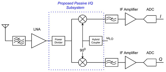
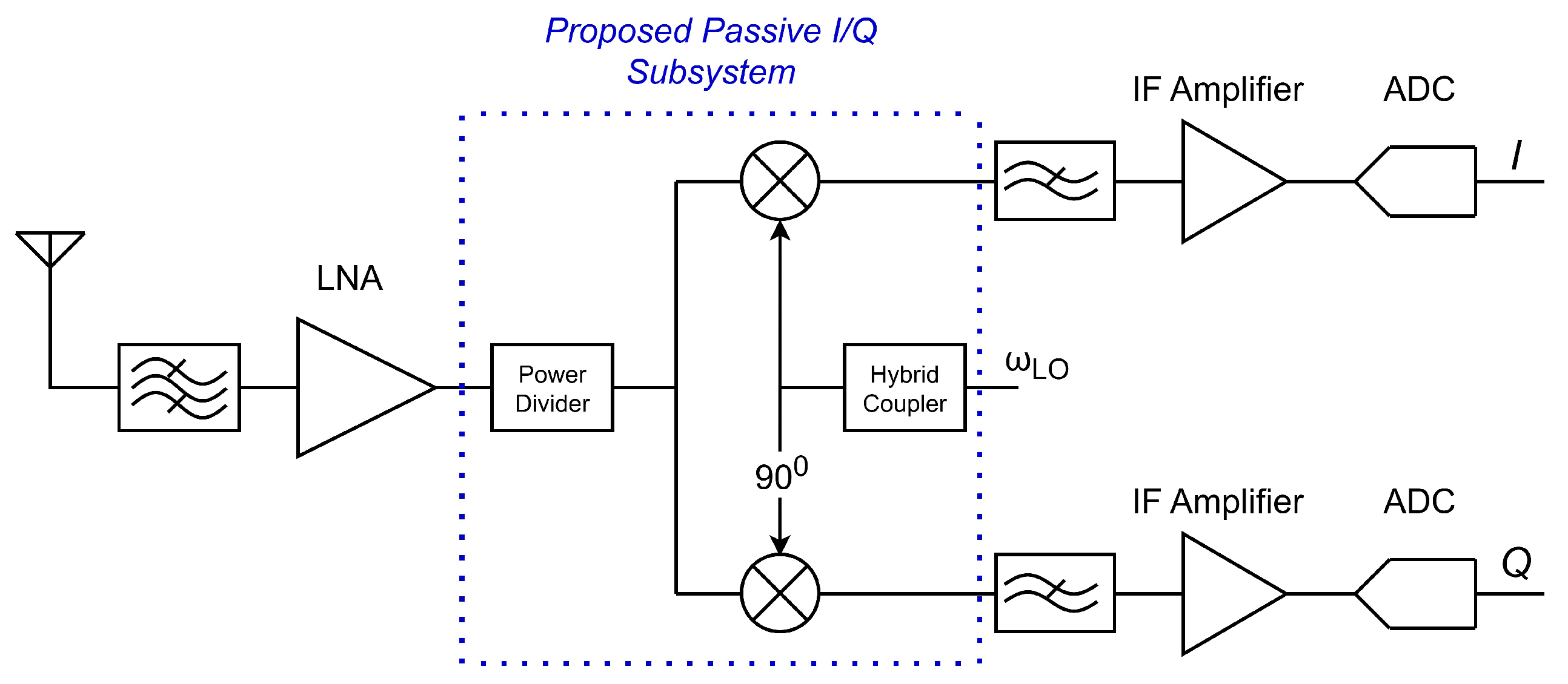
This section presents the design methodology and implementation of the proposed passive I/Q signal-generation subsystem. Figure 1 illustrates the complete X-band DCR architecture, with the proposed subsystem highlighted. The remaining receiver stages are included for context, illustrating how the proposed module integrates into a full maritime radar receiver front-end.
Figure 1.
Block diagram of the complete DCR signal chain. The highlighted passive I/Q subsystem, proposed and evaluated in this work, comprises the RF power divider, the hybrid coupler, and the single-balanced passive mixer.
The implementation of X-band passive microwave subsystems presents several challenges and design complexities, including increased sensitivity to fabrication tolerances, parasitic effects, and layout discontinuities, as well as the need to maintain accurate amplitude and phase balance throughout the I/Q signal paths. To address these challenges, the design and evaluation process combines analytical modeling, full-wave electromagnetic simulation, and layout-aware optimization. This approach ensures close agreement between the simulated and fabricated performance. Particular attention was paid to amplitude and phase balance, insertion loss, isolation, and linearity, as these parameters directly affect sideband suppression and baseband signal integrity in DCR operation.
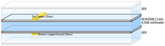
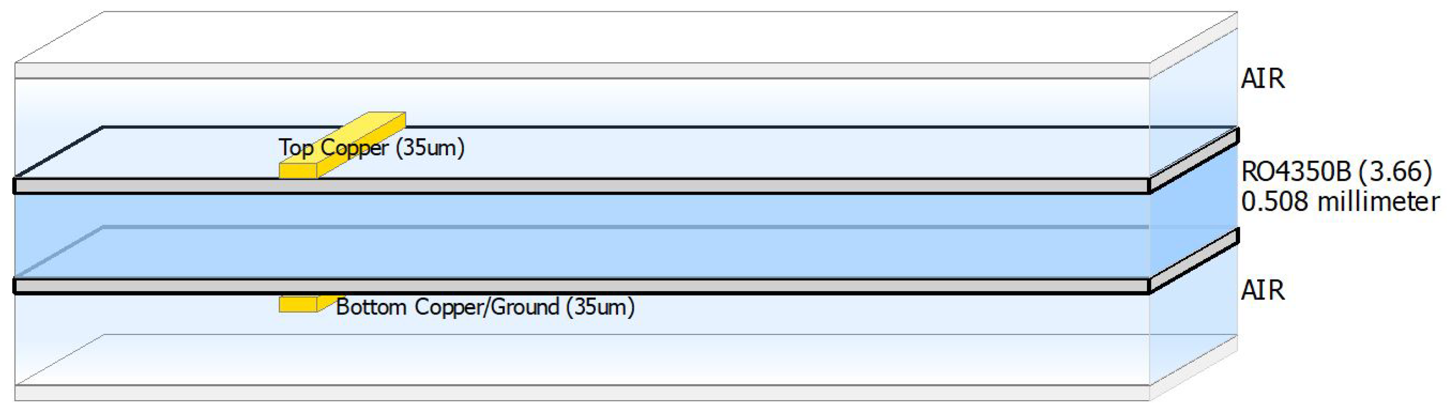
The common PCB stackup employed for the EM simulations and fabricated passive structures is illustrated in Figure 2. All passive circuits were implemented on a two-layer Rogers RO4350B substrate using microstrip transmission-line techniques. Full-wave EM simulations were carried out in Keysight ADS in order to accurately model the passive structures prior to fabrication.
Figure 2.
PCB stackup employed for the EM simulations and fabricated passive structures.
3.2. Theoretical Analysis of the Power Divider
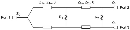
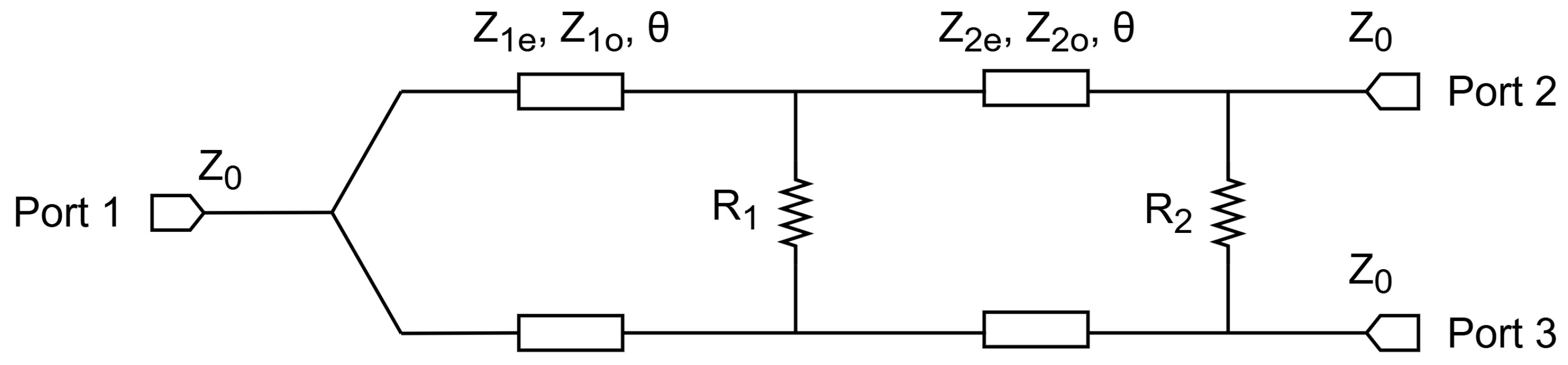
The power divider circuit is positioned immediately after the LNA and bandpass filter (BPF) stages to generate two identical RF signal paths. The proposed implementation follows a symmetric coupled-line configuration consisting of two transmission-line sections of equal electrical length l, each terminated with a discrete resistor at the output (Figure 3). The small spacing between the coupled-line branches enables direct placement of the termination resistors without requiring a ring-shaped geometry typically used in conventional Wilkinson dividers [24]. This characteristic supports reliable operation at high frequencies while maintaining a compact physical footprint, making the structure suitable for X-band applications.
Figure 3.
Block diagram of the proposed dual-band Wilkinson power divider based on coupled-line implementation.
The coupled-line sections, characterized by their even- and odd-mode impedances and , and an electrical length , provide the required impedance transformation. The two termination resistors further improve isolation and ensure proper output impedance matching, both critical requirements for stable high frequency operation [24]. Compared with conventional Wilkinson power dividers, the coupled-line implementation introduces additional design flexibility through the selection of the even- and odd-mode impedances and the corresponding coupling levels of the transmission-line sections. This additional degree of freedom enables broadband impedance transformation while maintaining proper output matching and port isolation over a wider frequency range.
To quantify the line parameters and validate the design, the electrical behavior of the divider was derived using even–odd mode analysis, following standard formulations in [23]. To achieve broadband operation, a frequency ratio of (>2) was selected. This requirement leads to an electrical length of for each coupled-line section. Assuming a system characteristic impedance of , the corresponding even-mode impedances and were calculated to be and , respectively.
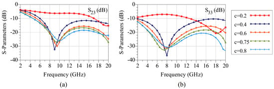
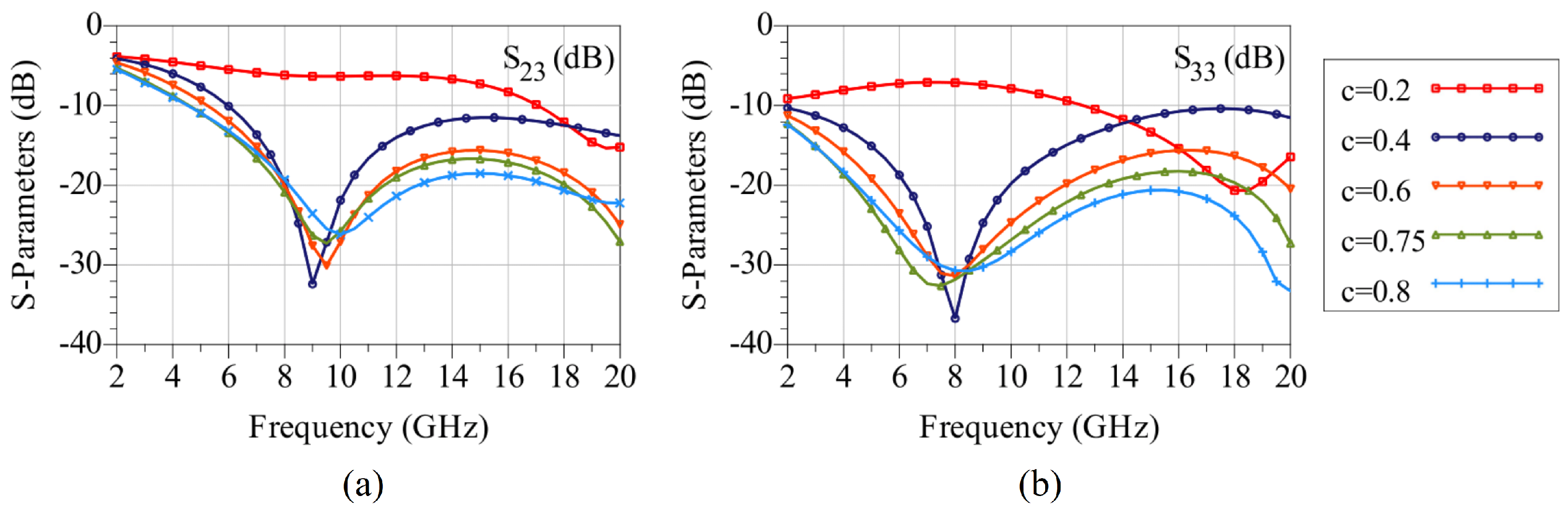
With the even-mode impedances established, the next step involves determining the coupling coefficient in order to determine the corresponding odd-mode impedances of the coupled-line structure. Figure 4a illustrates the simulated response of , corresponding to the isolation between the output ports, while Figure 4b presents the simulated response of , representing the output return loss (with due to circuit symmetry), for different values of the coupling coefficient ratio . When , the simulated response exhibits poor matching and limited isolation. As c increases beyond approximately , the responses converge toward improved performance, indicating a substantial improvement in both output return loss and isolation. Consequently, a coupling-coefficient value of was selected, as it provides a balance between electrical performance and manufacturability, considering the physical layout constraints.
Figure 4.
Simulated responses of (a) and (b) as functions of the coupling coefficient c.
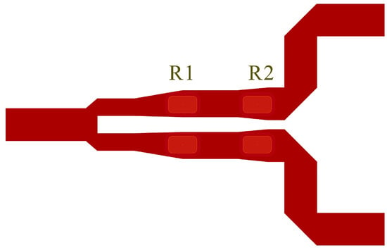
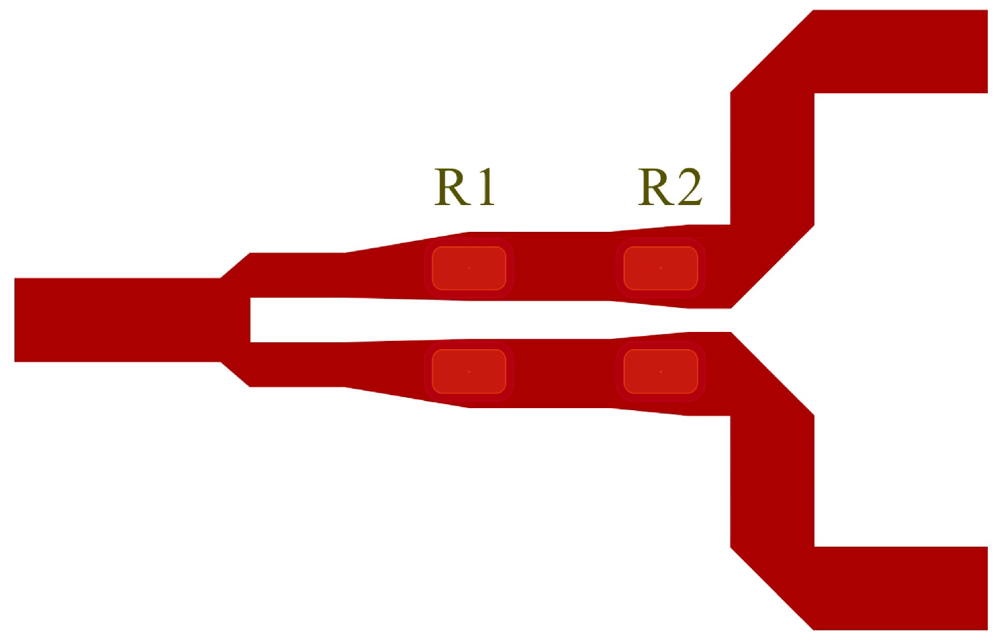
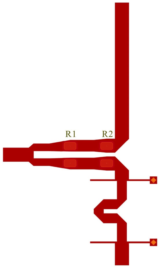
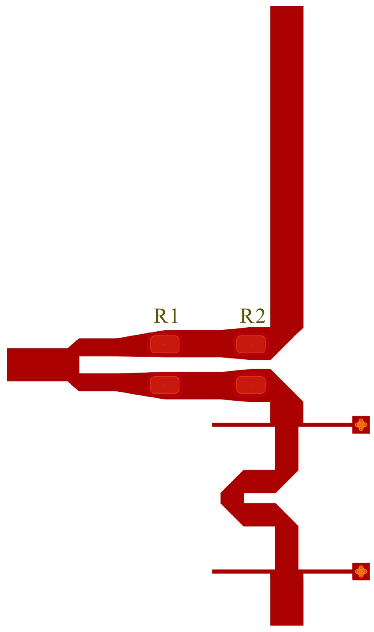
Following the selection of the coupling coefficient, the remaining electrical parameters of the divider were derived accordingly. The odd-mode characteristic impedances were calculated as and , while the resistor values and were determined to be and , respectively. The final layout implementation employed transmission-line widths of mm and mm, with corresponding spacings of mm and mm. Standard 0603 SMD resistor packages were selected to ensure placement accuracy while minimizing parasitic effects and microstrip discontinuities that could otherwise degrade high-frequency performance. Figure 5 presents the layout of the implemented Wilkinson power divider, including the integrated resistors and .
Figure 5.
The layout of the implemented Wilkinson power divider.
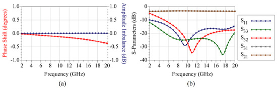
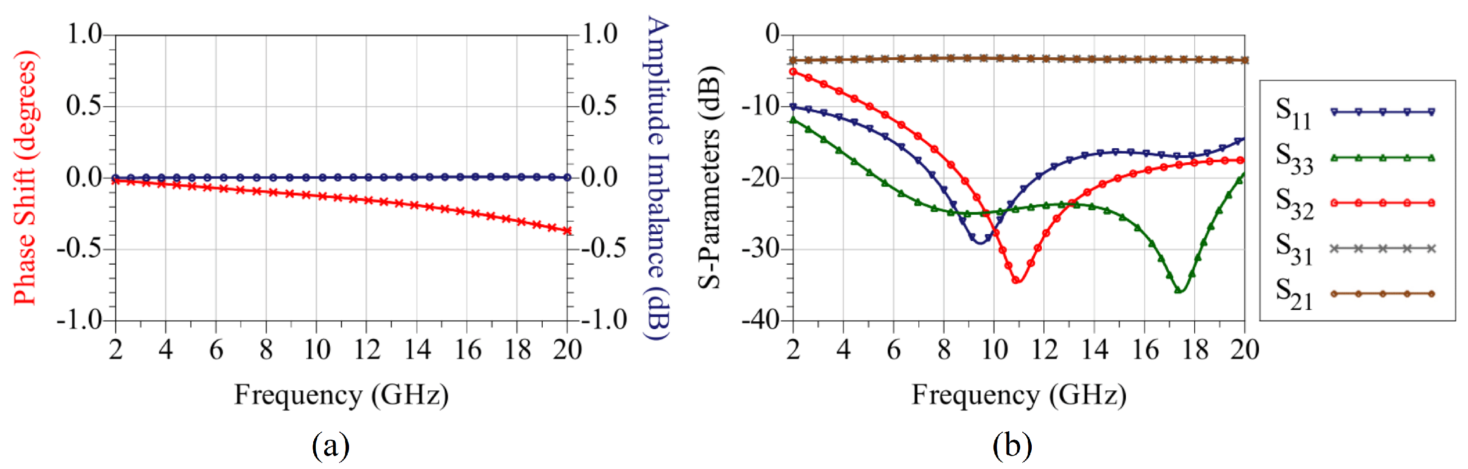
The performance of the finalized layout was verified through full-wave electromagnetic simulation to confirm broadband behavior and suitability for X-band implementation. The results of the FEM-based simulations are presented in Figure 6. As shown in Figure 6a, the power imbalance remains negligible across the range 2–20 GHz. The phase deviation does not exceed at 20 GHz and remains close to zero throughout the operating band, indicating stable and well-balanced performance. In addition, Figure 6b shows that the return loss at all ports and the port-to-port isolation remain better than 10 dB across the entire frequency span. Performance further improves within the 8–20 GHz range, where both metrics exceed 15 dB, while values above 20 dB are achieved within the 9.20–9.50 GHz maritime radar allocation.
Figure 6.
Full-wave FEM-simulated frequency responses of the proposed power divider: (a) amplitude and phase imbalance; (b) S-parameter responses.
3.3. Theoretical Analysis of the Phase Shifter
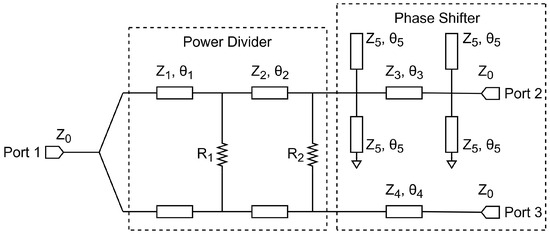
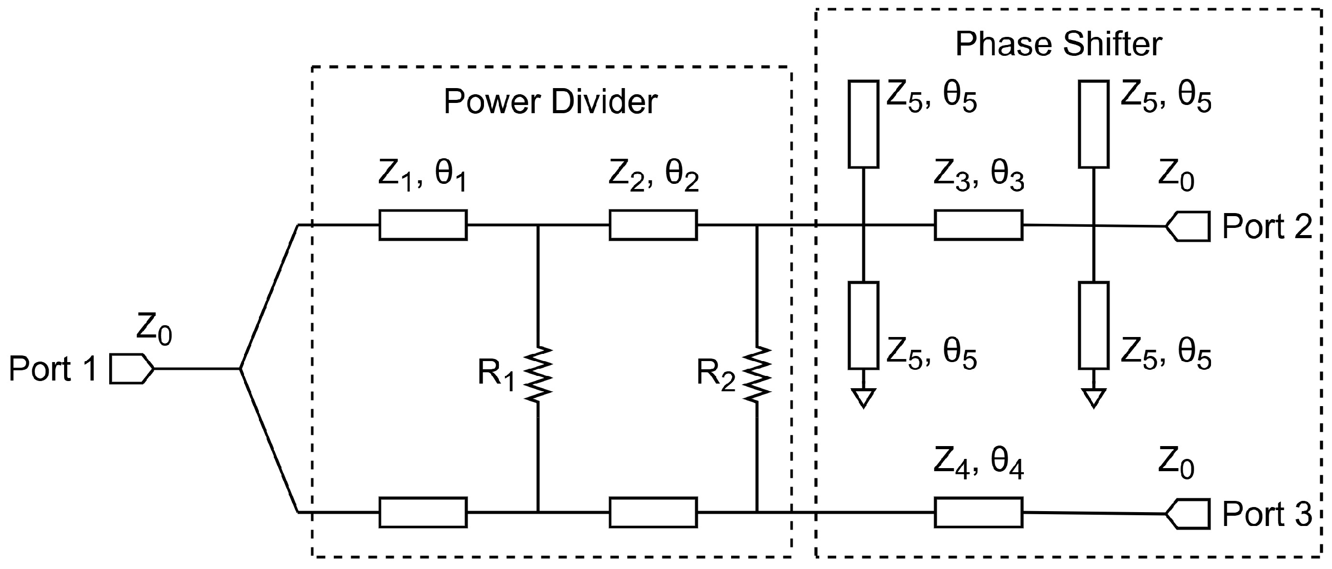
The LO signal path employs a power divider to ensure equal amplitude distribution between the mixer branches, while a precise phase shift is required to enable accurate I/Q demodulation. In the proposed implementation, this functionality is achieved by combining a dual-band Wilkinson power divider with a broadband phase-shifting network based on uncoupled transmission-line sections, enabling stable quadrature operation across the intended frequency band.
Figure 7 illustrates the equivalent circuit of the proposed hybrid coupler. Following the dual-band Wilkinson division stage described in Section 3.2, the LO signal is fed into the broadband phase-shifting network, which establishes the required quadrature LO phase relationship to drive the I and Q mixer branches. The phase-shifting network comprises a main transmission line of length and impedance ; a reference line of length and impedance ; and two additional stubs with impedance , terminated in open- and short-circuited ends, respectively.
Figure 7.
Block diagram of the proposed hybrid coupler.
The broadband behavior of the phase-shifting network is achieved through the phase compensation introduced by the parallel open- and short-circuited stubs in conjunction with the main transmission path. In conventional transmission lines, phase varies linearly with frequency. Compared with conventional transmission-line phase shifters, the inclusion of properly dimensioned open- and short-circuited stubs compensates for this variation, equalizing the phase response between the two signal paths [52]. Consequently, a nearly constant relative phase difference is preserved over a wide frequency range, making the structure well suited for broadband applications. This stability strongly depends on the appropriate selection of the stubs’ characteristic impedance, which determines the overall performance of the phase-shifting network.
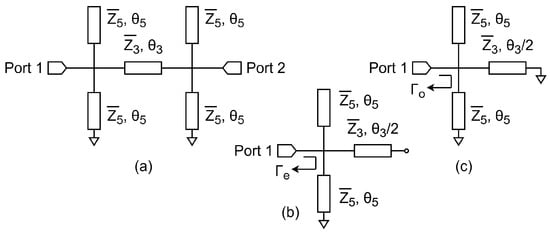
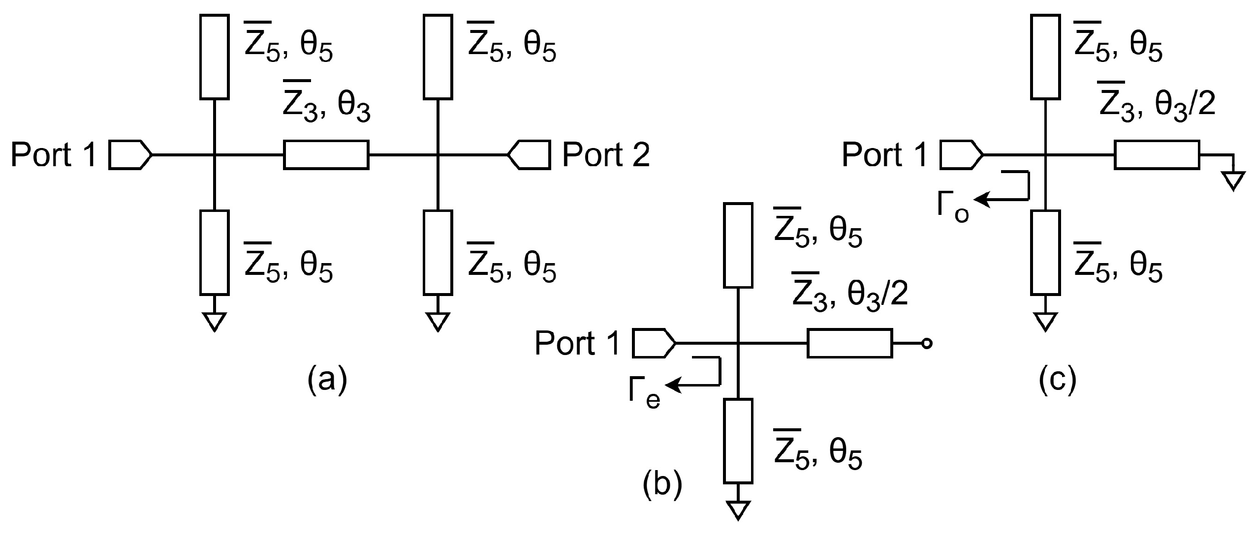
Figure 8a illustrates the circuit representation of the phase-shifting network. To facilitate this analysis, the even–odd mode decomposition method is applied, allowing the overall excitation to be separated into two independent cases. The corresponding equivalent circuits for the even and odd modes are shown in Figure 8b and Figure 8c, respectively.
Figure 8.
(a) The normalized equivalent circuit of the proposed phase shifter; (b) even-mode and (c) odd-mode equivalent circuits.
Based on these equivalent circuits, the scattering parameters of the proposed phase-shifting network can be expressed in terms of the reflection coefficients and , corresponding to the even- and odd-mode excitations. The fundamental relations are given by:
The reflection coefficients are obtained from the input impedance of the two equivalent circuits, , and the system characteristic impedance , namely:
The key performance parameter of the hybrid coupler is the differential phase between its two output ports, since it directly determines the quadrature accuracy of the LO signals driving the I/Q mixer branches. This parameter is defined as:
Ideally, across the entire operating bandwidth. In practical implementations, however, the system performance strongly depends on the stability of across the target operating bandwidth. Consequently, maintaining low input return loss and minimizing phase imbalance between the output ports were established as primary design objectives. Based on these requirements, the characteristic impedances , , and were determined through a parametric optimization procedure.
Building on the theoretical formulation, the broadband 90° hybrid coupler was synthesized and optimized to achieve two key design objectives: an input return loss better than dB and a maximum phase imbalance below across the 9–11 GHz operating band. Full-wave electromagnetic simulations were employed to extract and refine the transmission-line parameters, yielding optimal characteristic impedances of , , and . The corresponding physical widths were determined as , , and , ensuring that the implemented geometry accurately reproduces the intended impedance profile and satisfies the broadband quadrature requirement. Figure 9 presents the layout of the implemented 90° hybrid coupler (the orange circular symbols denote grounding vias).
Figure 9.
The layout of the implemented 90° hybrid coupler.
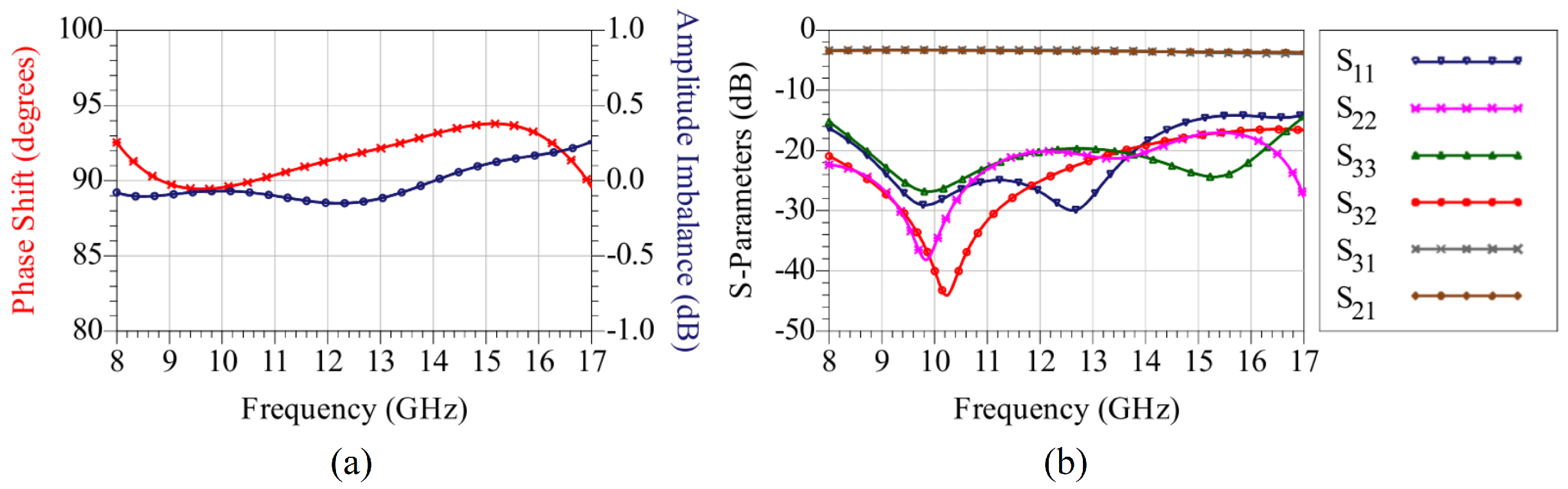
The performance of the finalized layout was assessed through full-wave electromagnetic (FEM) simulations, and the resulting responses are presented in Figure 10. As shown in Figure 10a, across the 8–17 GHz range, the amplitude response demonstrates excellent balance, with a maximum power imbalance of only 0.2 dB across the entire simulated band. Similarly, the phase error remains below across the full band and becomes negligible within the maritime radar allocation (9.20–9.50 GHz). In addition, Figure 10b shows that all port return-loss values and the isolation between the output ports remain better than 14 dB, confirming the broadband nature of the proposed structure. Within the X-band, the performance improves further, exhibiting return-loss and isolation levels better than 22 dB. These results confirm that the proposed network achieves stable broadband operation while meeting the stringent quadrature requirements of the intended application.
Figure 10.
Full-wave FEM-simulated frequency responses of the proposed hybrid coupler: (a) amplitude and phase imbalance; (b) S-parameter responses.
3.4. Theoretical Analysis of the Single-Balanced Passive Mixer
Mixers are fundamental components in RF front-end architectures, enabling frequency translation through nonlinear interaction between the RF input and the local oscillator (LO) signal. This process produces sum and difference frequency components, along with higher-order harmonics. The linearity, isolation, and conversion loss of the mixer are key factors that directly determine the overall front-end performance.
Single-ended mixer implementations exhibit low efficiency and are therefore rarely used in modern RF systems. A more efficient approach employs two switching elements driven by differential LO signals, effectively commutating the RF signal. This topology, known as a single-balanced mixer, improves conversion efficiency and provides partial suppression of LO–RF feedthrough. However, LO–IF feedthrough remains significant. Further suppression of LO-IF feedthrough can be achieved using a double-balanced topology, which employs both differential LO and RF signals to cancel unwanted components [51].
In the direct-conversion architecture considered in this work, the IF is centered at baseband, allowing the undesired LO-IF feedthrough component to be attenuated using a properly designed low-pass filter (LPF). In addition, since the RF and LO frequencies coincide, the resulting spurious components are further attenuated by the LPF response.
Double-balanced mixers exhibit increased implementation complexity due to the requirement for baluns, precise device matching, and additional components, often resulting in higher conversion loss and increased parasitic effects compared to single-balanced implementations.
Given its reduced complexity, lower conversion loss, and single-layer implementation, the single-balanced mixer is selected as the most suitable solution for the proposed design. This topology provides sufficient isolation for the intended application while maintaining a favorable trade-off between performance and implementation complexity.
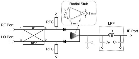
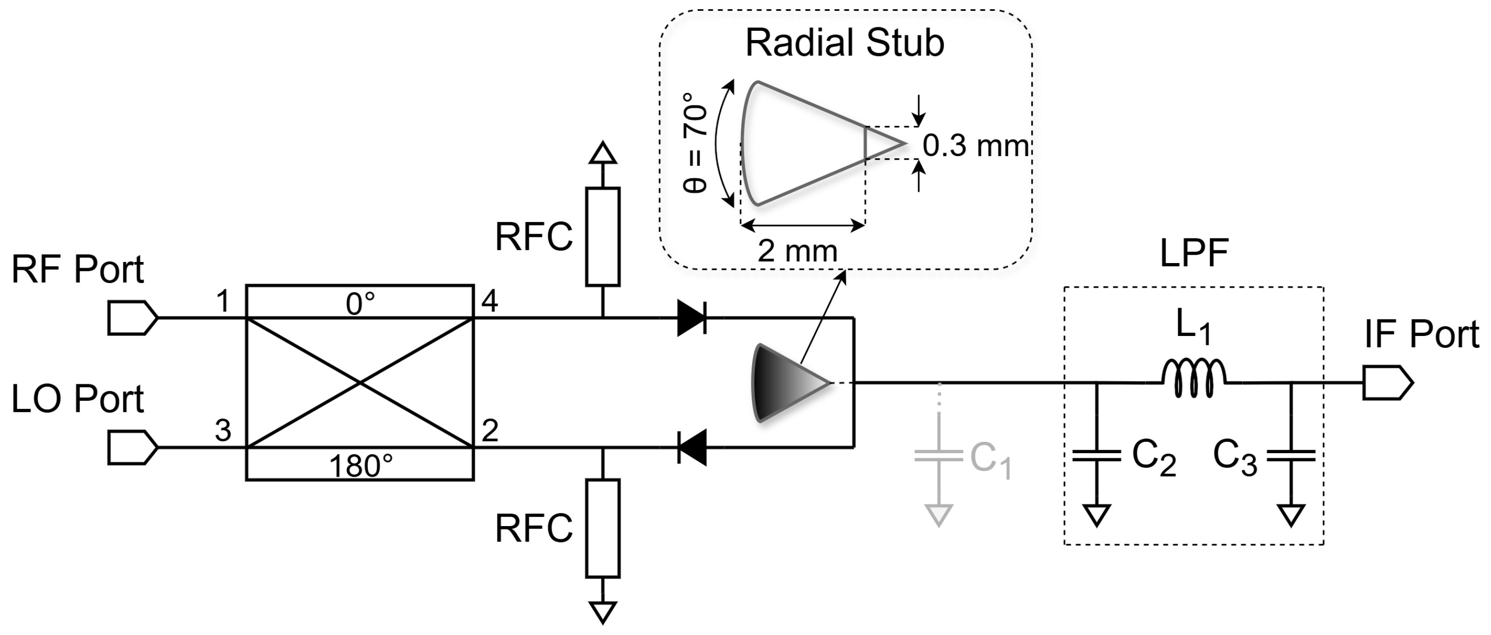
The schematic diagram of the proposed mixer architecture is shown in Figure 11. The RF and LO signals are applied to the sum and difference ports of a rat-race coupler, respectively. The RF signal is split equally and remains in phase at both paths, while the LO signal exhibits a phase difference, alternately driving the two Schottky diodes into conduction. One diode conducts while the other remains reverse-biased at any given moment. This alternating conduction samples the RF signal, enabling the nonlinear mixing process.
Figure 11.
Block diagram of the proposed single-balanced passive mixer.
The common node of the two diodes collects the mixing products, which are routed through a low-pass filter (LPF) to suppress the undesired harmonic content and retain only the IF component. A capacitor is conventionally placed at the IF node to attenuate any residual RF and LO leakage. However, electromagnetic simulations showed that replacing this capacitor with a radial stub tuned at the RF and LO center frequencies yields improved linearity performance. The radial stub behaves as a short circuit at RF and LO frequencies— thereby blocking leakage toward the output—while presenting an open-circuit behavior at the low IF frequency, allowing the IF signal to pass with minimal attenuation. This approach effectively suppresses RF and LO leakage toward the IF port while establishing a well-defined impedance environment at the diode output node.
In practice, at X-band frequencies, conventional SMT bypass capacitors exhibit non-negligible parasitic inductance, which degrades the RF-to-DC isolation and partially loads the RF path through the bias network. In contrast, the radial stub provides improved RF-to-DC isolation at X-band frequencies, while the SMT capacitors remain effective at lower frequencies.
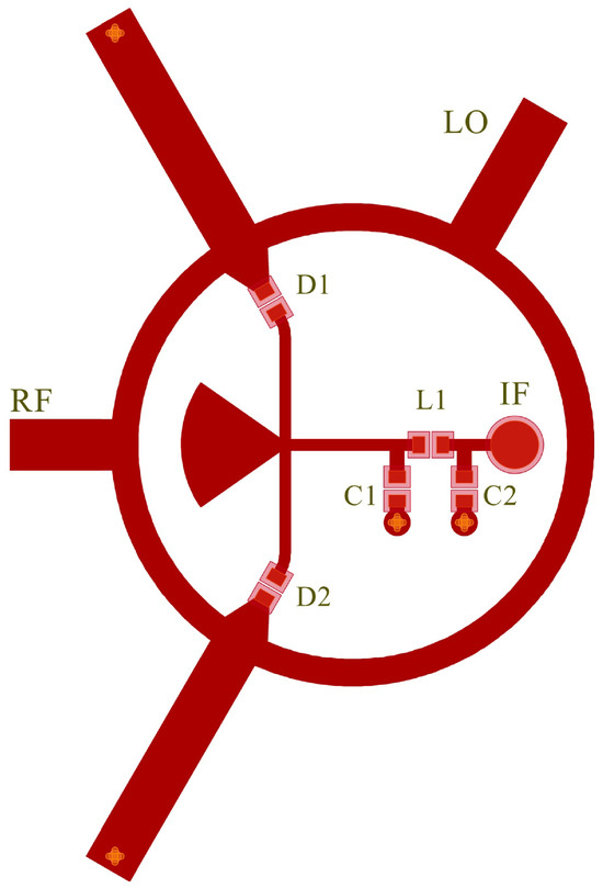
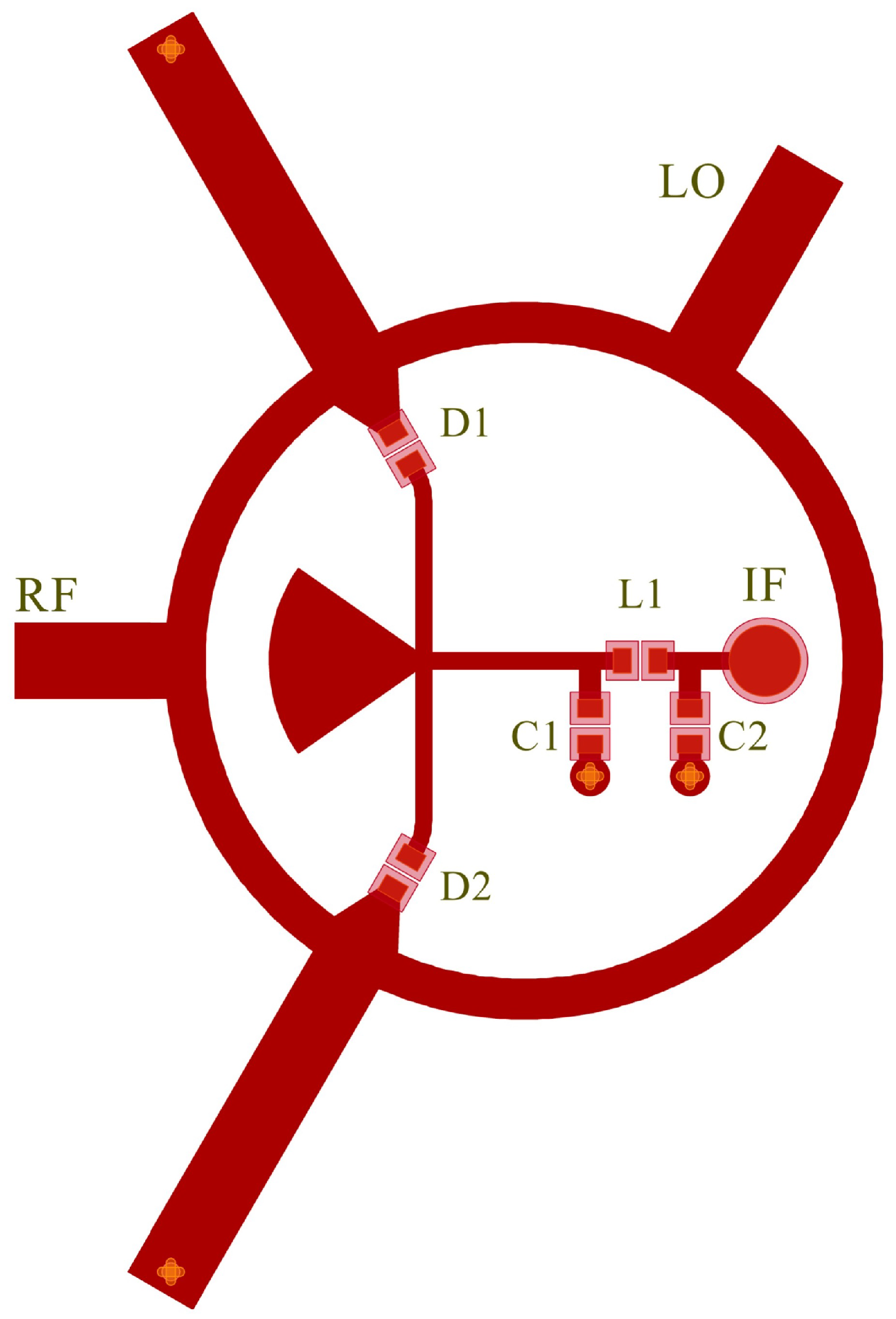
At high LO drive levels, the Schottky diodes tend to self-bias, generating an undesired DC component that increases the conversion loss and degrades port-to-port isolation. To prevent this phenomenon, a DC grounding path is required without disturbing the RF characteristics of the circuit. This requirement is satisfied by incorporating two short-circuited stubs (RFCs), tuned at the RF and LO center frequencies. These stubs offer a low-impedance path to ground for the DC component and low-frequency IF components, while presenting a high impedance at the RF and LO frequencies. As a result, the diodes operate under stable biasing conditions, and the mixer operation remains stable. Figure 12 presents the layout of the implemented single-balanced passive mixer (the orange circular symbols denote grounding vias).
Figure 12.
The layout of the implemented single-balanced passive mixer.
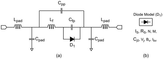
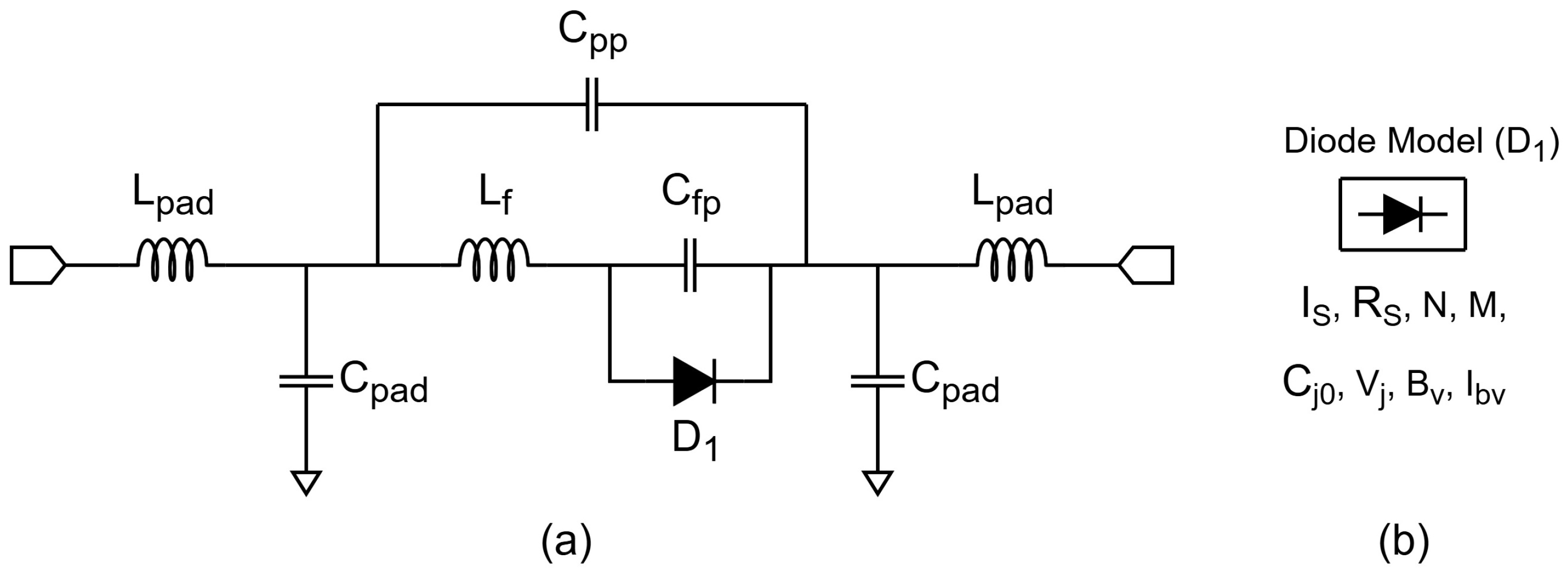
For the implementation of the proposed single-balanced mixer, the commercially available GaAs Schottky diode MA4E1317 (MACOM; Lowell, MA, USA) was selected owing to its low junction resistance and junction capacitance. The large-signal equivalent-circuit model parameters, comprising both parasitic components (Figure 13a) and nonlinear (SPICE) elements (Figure 13b), were obtained using the extraction procedure described in [53] and incorporated into the simulation environment. The complete set of extracted parameters is summarized in Table 1 and Table 2 [53].
Figure 13.
Parasitic component parameters (a) and nonlinear SPICE parameters (b) of the large-signal equivalent model of the MA4E1317 Schottky diode.
Table 1.
Parasitic parameters of the MA4E1317 Schottky diode.
Table 2.
Nonlinear SPICE model parameters of the MA4E1317 Schottky diode.
Based on the preceding analysis and the extracted large-signal diode model, the proposed single-balanced mixer was designed to meet several critical and often competing performance requirements. Specifically, the mixer must achieve low conversion loss (target ), high linearity (input-referred ), and high port-to-port isolation (>30 dB). Achieving these specifications simultaneously in a compact, fully passive architecture is particularly challenging, especially for X-band maritime applications.
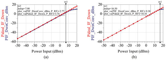
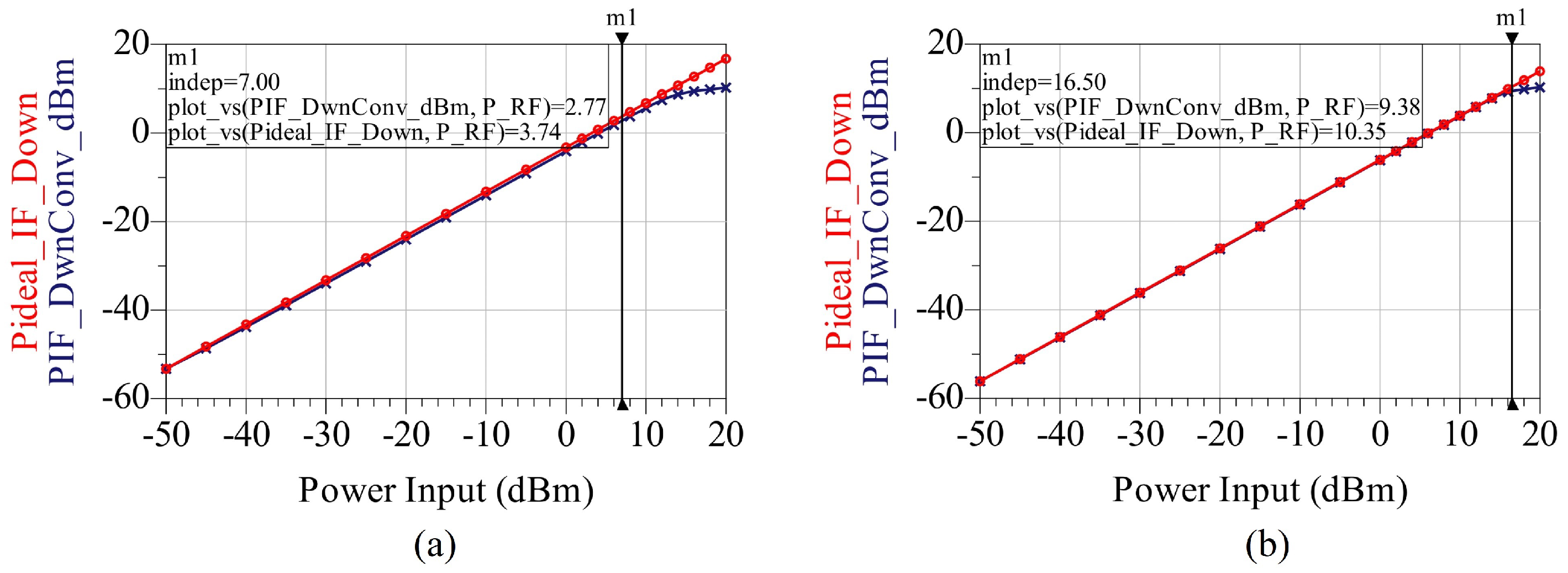
To evaluate the proposed structure, Figure 14 compares the EM simulation results for two IF-node topologies: (a) a conventional bypass capacitor and (b) a radial stub tuned at . The simulations, performed at with , show that replacing the capacitor with the radial stub results in improved linearity. A relatively high LO drive level is used to ensure proper switching of the Schottky diodes. As a result, the input-referred 1-dB compression point increases from to , due to the reduced parasitic capacitance and the higher out-of-band impedance of the radial stub, which provides improved RF/LO termination at the IF node and reduces leakage toward the output.
Figure 14.
Comparison of the input-referred 1-dB compression point () of the mixer at and for the two IF-node implementations: (a) bypass capacitor and (b) radial stub tuned at .
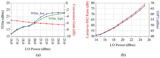
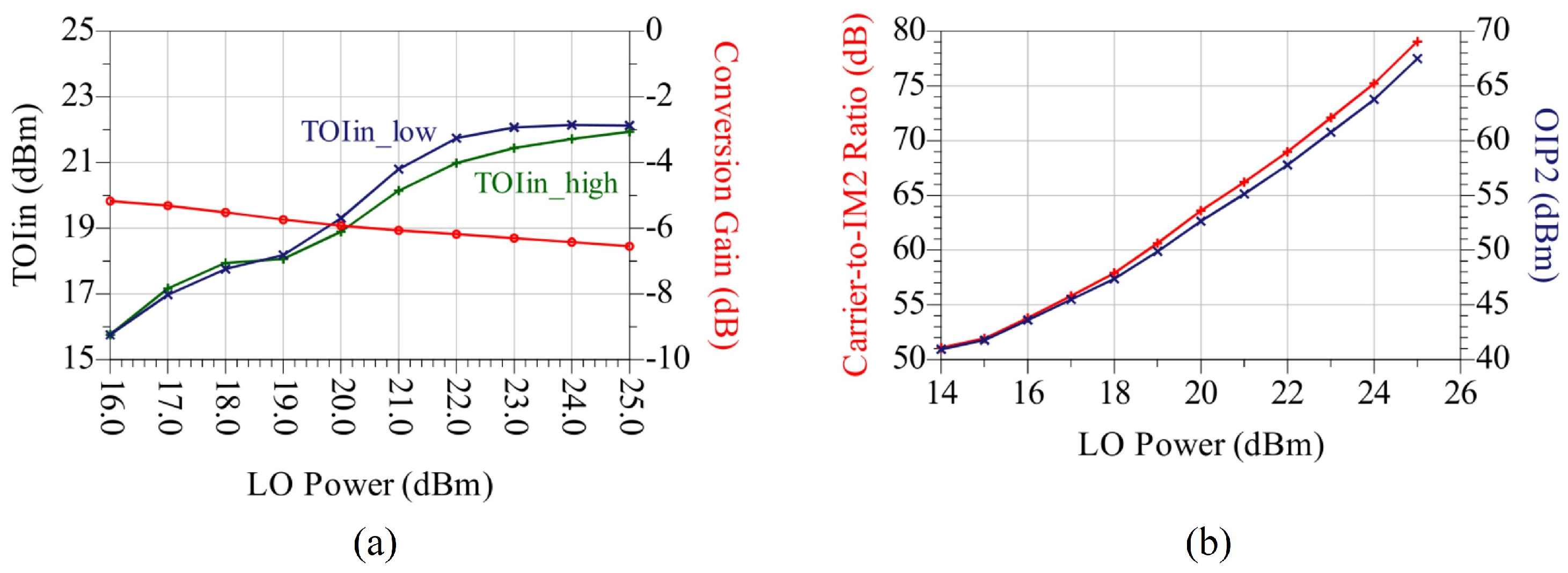
In addition to the 1-dB compression point, the linearity of the mixer was assessed through second- and third-order intercept points, which are key metrics for evaluating mixer linearity in direct-conversion architectures. Figure 15a illustrates the input third-order intercept point () as a function of LO drive power, together with the corresponding conversion loss. As the LO power increases, the improves from at to at . This trend is consistent with the improved switching behavior of the Schottky diodes under higher LO drive levels.
Figure 15.
Mixer linearity versus LO drive power : (a) input third-order intercept point (TOIin) and conversion loss; (b) output second-order intercept point (OIP2) and carrier-to-IM2 ratio.
Moreover, Figure 15b presents the output second-order intercept point () together with the carrier-to-IM2 ratio as functions of LO drive power. Both metrics increase monotonically with , reaching values up to for at the highest excitation level. This behavior indicates effective suppression of second-order distortion products and high signal purity at the IF output. Overall, the linearity results demonstrate that the proposed mixer achieves stable performance and is well suited for high-dynamic-range X-band receiver applications.
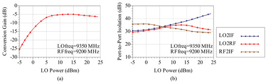
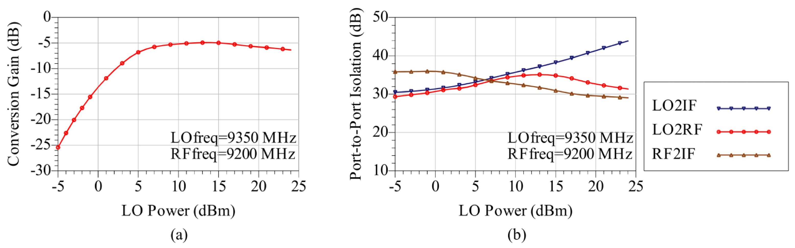
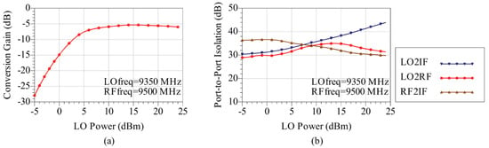
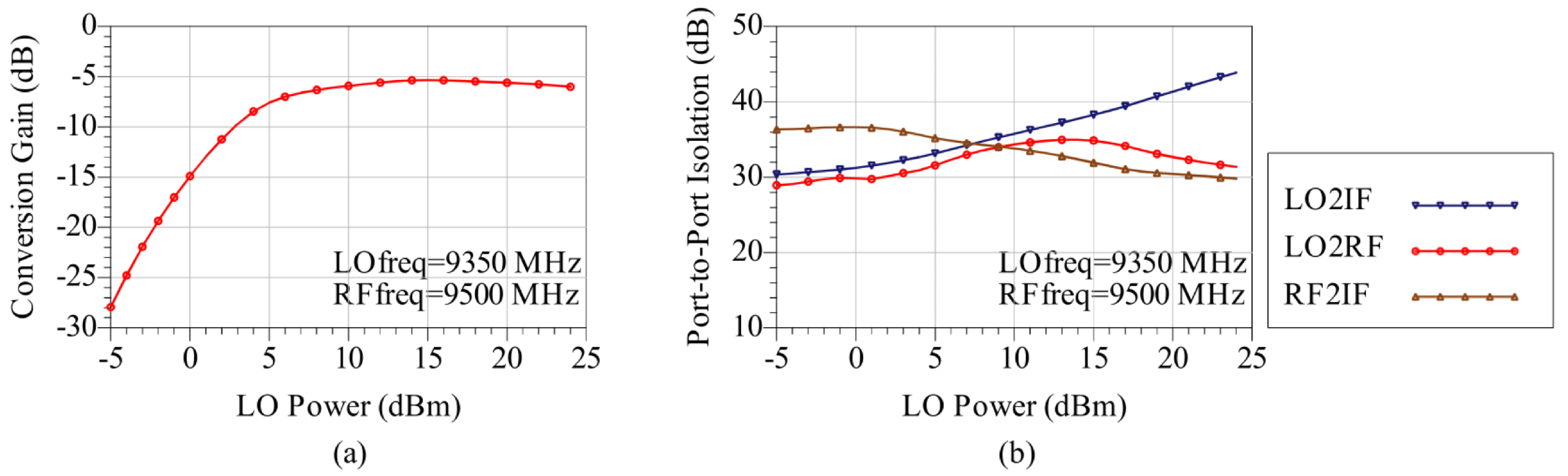
In addition to the linearity analysis, the mixer performance was further evaluated in terms of conversion loss and port-to-port isolation as functions of the LO drive level. Figure 16 and Figure 17 present the EM simulation results obtained at a fixed LO frequency of for two representative RF frequencies, and , corresponding to the lower and upper edges of the X-band maritime allocation.
Figure 16.
Conversion loss (a) and port-to-port isolation (b) of the mixer versus LO drive power , for and .
Figure 17.
Conversion loss (a) and port-to-port isolation (b) of the mixer versus LO drive power , for and .
As shown in Figure 16a and Figure 17a, the conversion loss decreases rapidly with increasing LO power and stabilizes for in the range of 5–5.5 dB, which is considered highly satisfactory for a single-balanced mixer architecture. The corresponding port-to-port isolation results, depicted in Figure 16b and Figure 17b, exceed across the entire LO power range. This behavior confirms the effectiveness of the hybrid-ring topology in combination with the matching networks in suppressing signal leakage between ports.
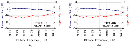
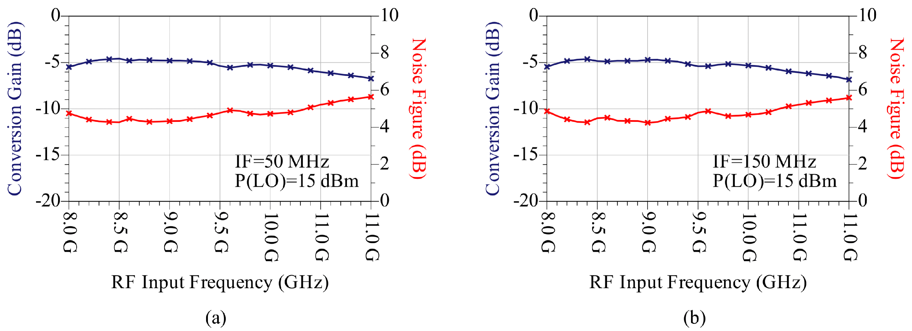
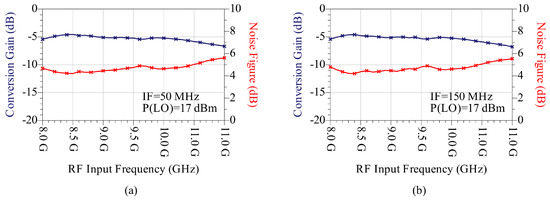
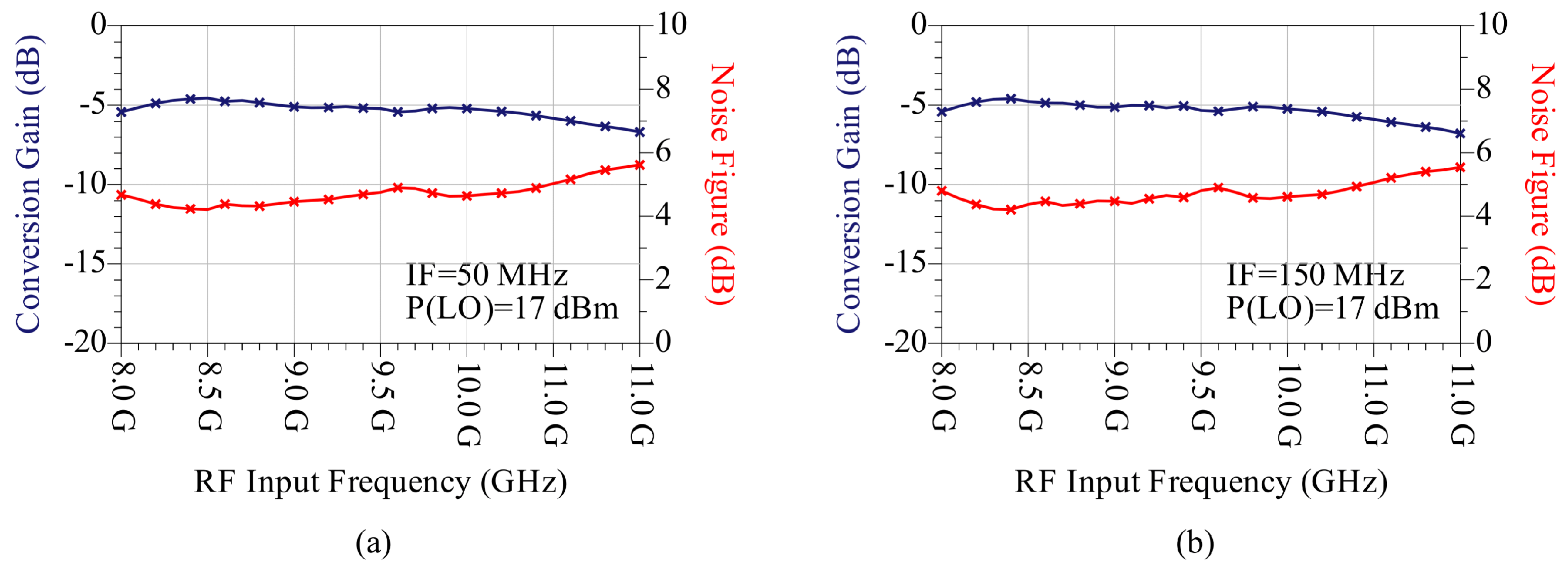
To further assess the broadband response of the proposed mixer, EM simulations were performed for RF frequencies ranging from to and for two IF frequency values, and , consistent with practical baseband frequency offsets in direct-conversion receivers. Figure 18 and Figure 19 present the simulated conversion loss and noise figure for two representative LO drive levels of and , respectively. The results indicate that the mixer response remains stable across the entire examined RF range, with the conversion loss maintained at approximately and the noise figure closely following the conversion loss, remaining near . This behavior demonstrates the broadband performance of the proposed mixer, further confirming its suitability for broadband direct-conversion X-band receiver applications.
Figure 18.
Conversion loss and noise figure of the mixer versus RF input frequency for at two IF frequencies: (a) and (b) .
Figure 19.
Conversion loss and noise figure of the mixer versus RF input frequency for at two IF frequencies: (a) and (b) .
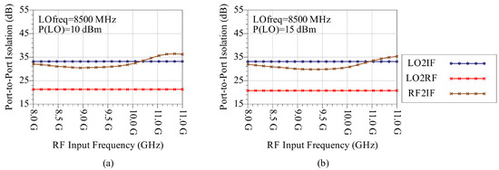
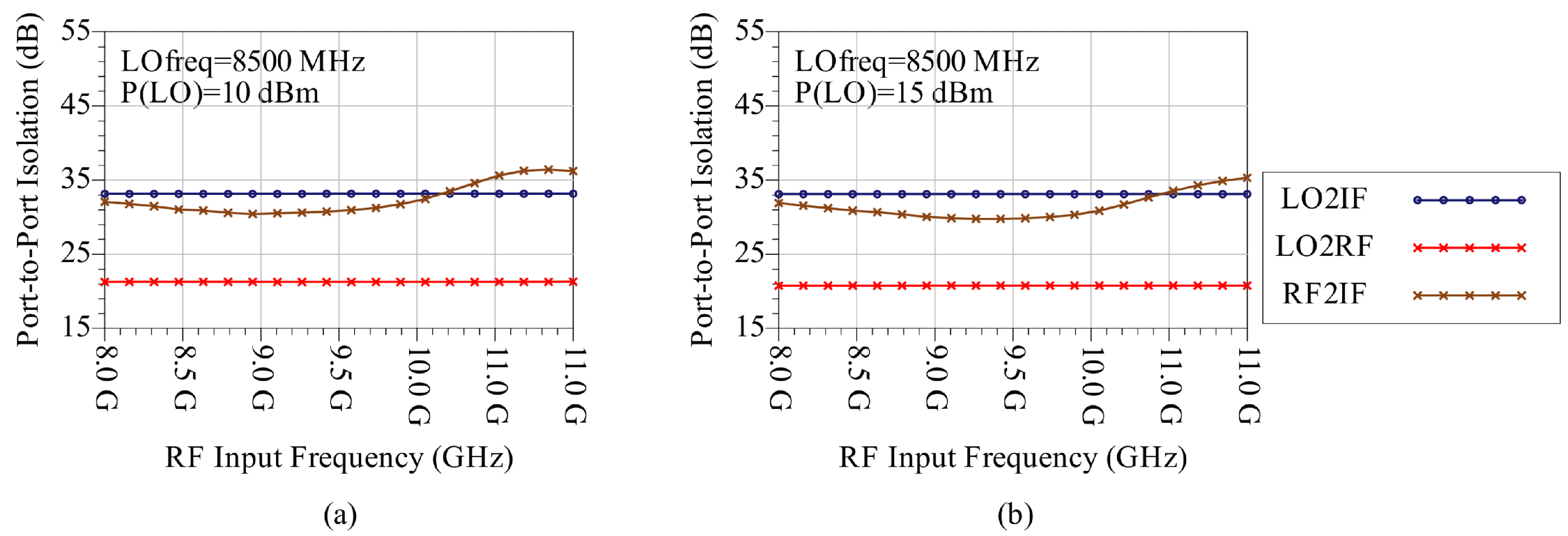
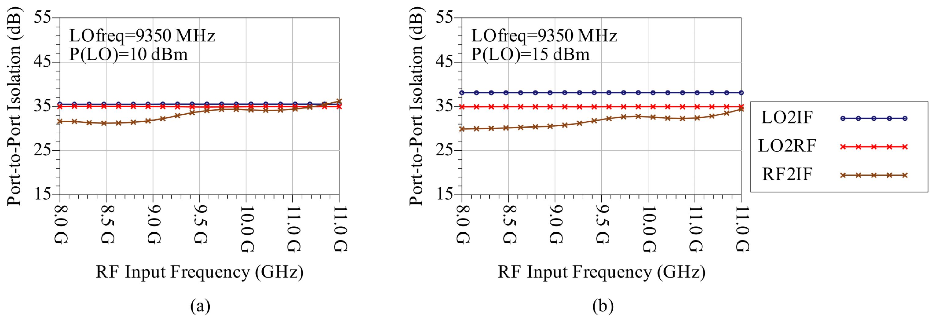
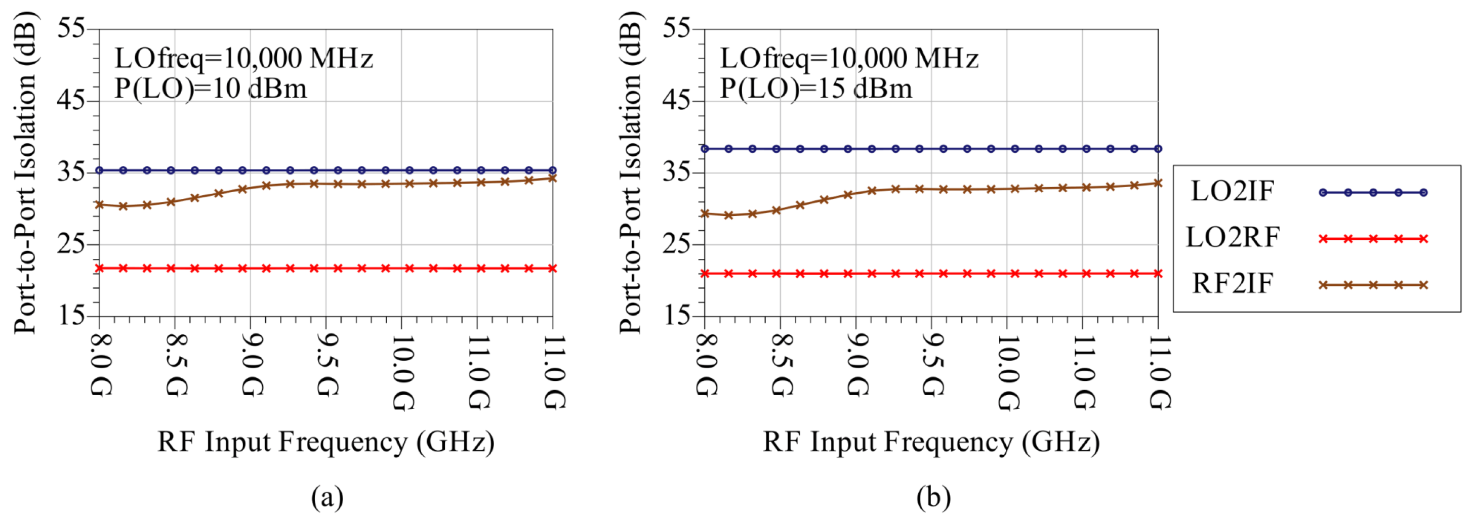
Finally, Figure 20, Figure 21 and Figure 22 present the port-to-port isolation performance of the mixer in the 8– RF band for different LO frequencies and drive levels. Specifically, LO frequencies of , , and are examined for LO drive levels of and . The results show that the LO-IF and RF-IF isolations remain consistently throughout the examined range, ensuring effective suppression of undesired coupling and stable mixer operation.
Figure 20.
Port-to-port isolation of the mixer versus RF input frequency for at different LO drive power levels : (a) and (b) .
Figure 21.
Port-to-port isolation of the mixer versus RF input frequency for at different LO drive power levels : (a) and (b) .
Figure 22.
Port-to-port isolation of the mixer versus RF input frequency for at different LO drive power levels : (a) and (b) .
Particular emphasis is placed on LO-RF isolation, which is a critical parameter in direct-conversion receivers. At the nominal LO frequency of , the isolation exceeds , providing sufficient mitigation of LO leakage toward the RF port. However, at and , the isolation decreases to approximately , reflecting the bandwidth limitations and frequency-dependent imbalance of the hybrid and matching networks toward the edges of the operating band, while remaining within acceptable limits for practical operation.
4. Experimental Results
4.1. Measurement Setup and Calibration
For the experimental evaluation of both the power divider and the hybrid coupler, a Hewlett Packard (HP) HP8719D vector network analyzer (VNA) (Santa Rosa, CA, USA) was employed. Since the VNA is equipped with only two ports, the measurements were performed in successive configurations. In each configuration, two ports of the device under test were connected to the VNA, while the remaining port was terminated with a matched load to ensure proper termination conditions. Although high-quality 50 terminations were employed, practical matched loads exhibit a finite reflection coefficient, which may introduce a minor uncertainty in the measured isolation levels due to residual reflections from the terminated port. By repeating this procedure for all port combinations, the complete set of scattering parameters (S-parameters) was obtained.
The measurement frequency range was set from 8 to 12 GHz, covering the entire X-band region of interest. Prior to the measurements, a two-port calibration procedure was performed, with the calibration plane defined at the SMA connectors at the ends of the measurement cables, in order to minimize systematic errors due to cable and adapter losses.
For the interconnection between the circuits and the VNA, SMP-to-SMA coaxial adapters (Mini-Circuits 047-3SMPSM+; Brooklyn, NY, USA) were used. The total insertion loss of the measurement chain, including adapters and cables, was estimated to be approximately 2.5 dB over the frequency range of interest. This loss was taken into account during data post-processing, so that the reported results accurately reflect the intrinsic performance of the proposed circuits.
For the experimental evaluation of the single-balanced mixer, two identical signal generators (HP 83711B; Santa Rosa, CA, USA) were used: one for driving the local oscillator (LO) port and one for exciting the radio-frequency (RF) port. The intermediate-frequency (IF) output was monitored using a spectrum analyzer (HP 8592B; Santa Rosa, CA, USA), enabling the observation of the generated mixing products.
Following the calibration procedure, the actual RF input power delivered to the mixer was experimentally verified. A deviation of approximately 5 dB was observed with respect to the nominal output level indicated by the RF signal generator, and was independently confirmed using the VNA. Consequently, a correction factor of dB was applied to the reported RF input power levels to accurately reflect the effective excitation conditions at the RF port of the mixer.
The same SMP-to-SMA adapters were used for the mixer measurements, with their insertion losses also taken into account during data post-processing.
4.2. Experimental Characterization of the Power Divider
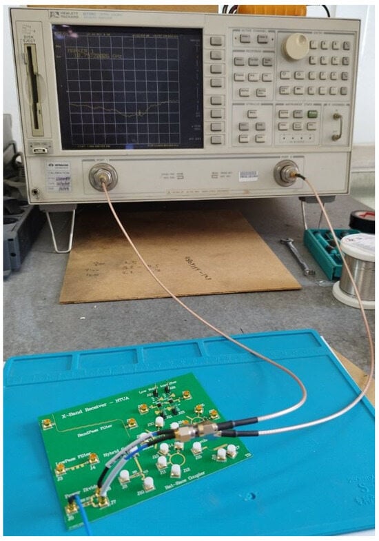
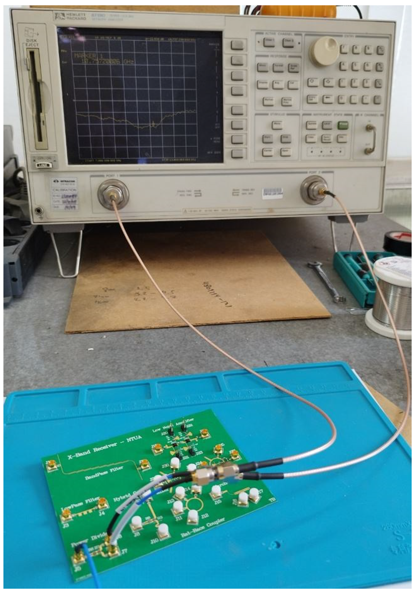
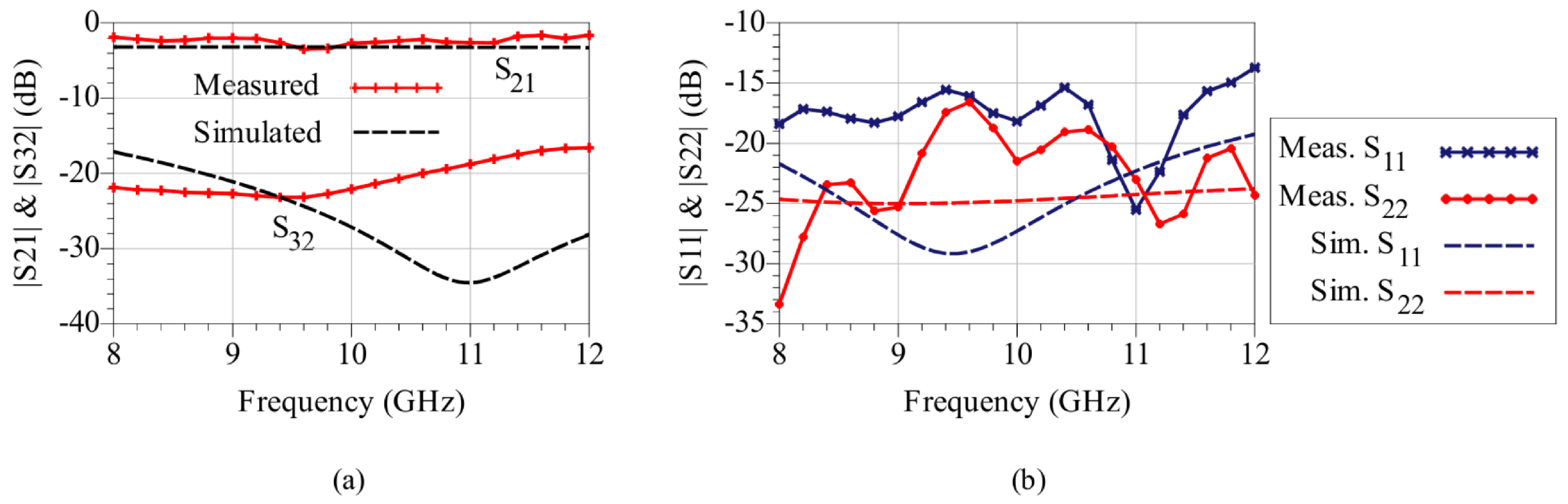
This subsection presents the measured S-parameter performance of the proposed power divider. Figure 23 shows the fabricated PCB together with the experimental measurement setup, which was also used for the characterization of the 90° hybrid coupler. Figure 24 and Figure 25 compare the simulated and measured responses over the 8–12 GHz frequency range.
Figure 23.
Measurement setup and fabricated PCB used for S-parameter characterization of the Wilkinson power divider and the 90° hybrid coupler using the HP 8719D vector network analyzer.
Figure 24.
Simulated and measured imbalance characteristics of the proposed power divider between the output ports: (a) phase imbalance and (b) amplitude imbalance, over the frequency range from 8 to 12 GHz.
Figure 25.
Simulated and measured S-parameter performance of the proposed power divider: (a) insertion loss () and output-port isolation (); (b) input and output return loss ( and ), with due to circuit symmetry.
Figure 24a and Figure 24b present the simulated and measured phase and amplitude imbalance between the two output ports, respectively. The phase imbalance remains within across the full frequency range and is further reduced to within in the 9.2–9.5 GHz band. The amplitude imbalance remains within dB, demonstrating an almost ideal equal power split between the output ports.
The transmission characteristics of the power divider are presented in Figure 25. Specifically, Figure 25a shows the simulated and measured insertion loss () and output-port isolation (). The response remains flat across the measured frequency range, with a value close to the ideal 3 dB power split. Due to the circuit symmetry, is nearly identical to , with a measured deviation within dB, and is therefore omitted for clarity. Good agreement between simulations and measurements is observed, with isolation levels better than 15 dB across the full band and exceeding 20 dB in the 9.2–9.5 GHz range.
Figure 25b presents the corresponding input and output return loss, represented by and , respectively, with being identical to due to circuit symmetry. All return-loss values remain better than 15 dB over the entire frequency range. The measured data have been post-processed to account for the insertion loss of the measurement setup, including cables and adapters, as well as residual phase offsets introduced by the measurement environment. Overall, the results verify the proper operation of the power divider and confirm its suitability as a building block for the proposed receiver architecture.
4.3. Experimental Characterization of the Hybrid Coupler
The measured performance of the proposed hybrid coupler is presented in this subsection. The characterization was performed under the same measurement conditions, using the experimental setup shown in Figure 23.
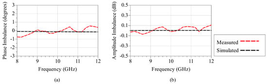
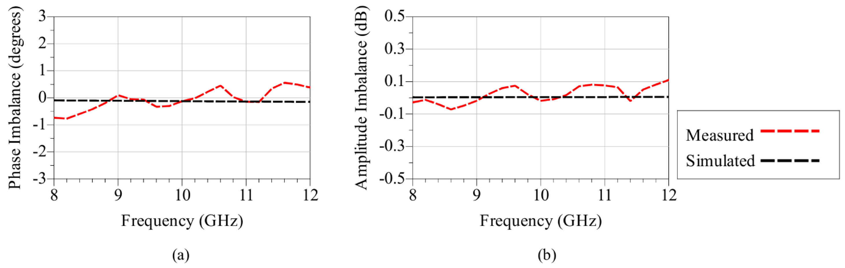
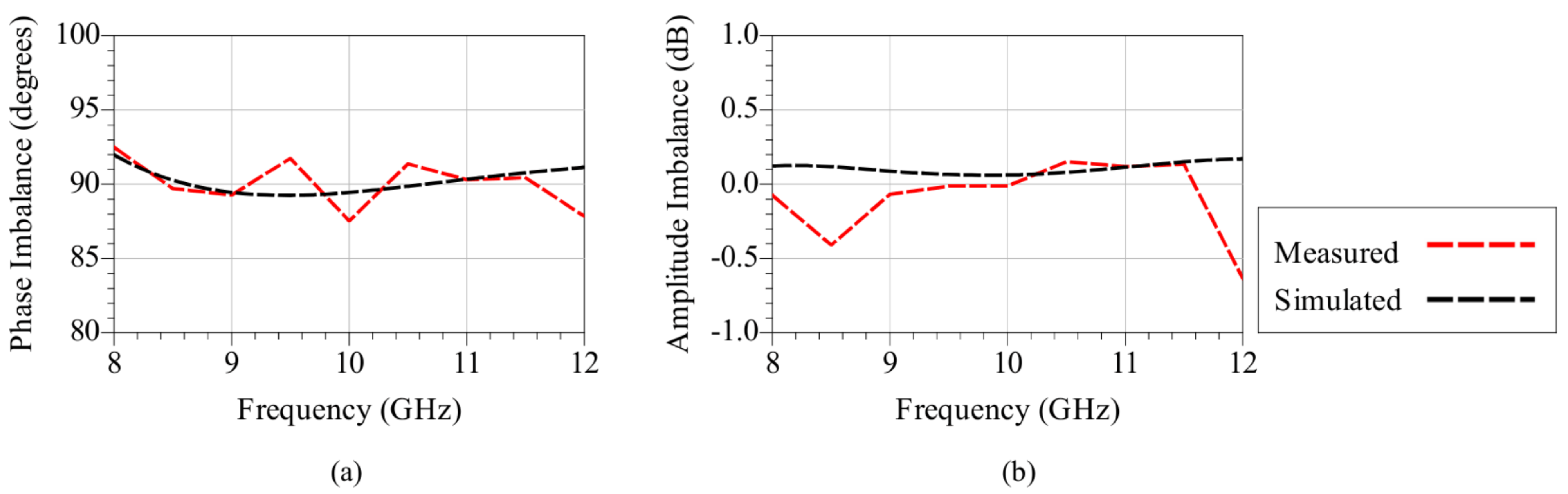
Figure 26a and Figure 26b present the simulated and measured phase and amplitude imbalance between the two output ports, respectively, over the 8 to 12 GHz frequency range. The phase imbalance remains within approximately across the full frequency range and is further reduced to within in the 9.2–9.5 GHz range, indicating stable quadrature operation. Similarly, the amplitude imbalance remains close to dB, demonstrating well-balanced power division between the output ports.
Figure 26.
Simulated and measured imbalance characteristics of the proposed hybrid coupler between the output ports: (a) phase imbalance and (b) amplitude imbalance, over the frequency range from 8 to 12 GHz.
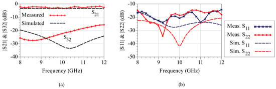
The transmission characteristics of the hybrid coupler are shown in Figure 27. Specifically, Figure 27a shows the simulated and measured insertion loss () and output-port isolation (). Due to circuit symmetry, closely follows the response of and is therefore omitted for clarity. The isolation between the output ports remains close to or better than 20 dB across the frequency range, confirming effective port decoupling.
Figure 27.
Simulated and measured S-parameter performance of the proposed hybrid coupler: (a) insertion loss () and output-port isolation (); (b) input and output return loss ( and ), with due to circuit symmetry.
Figure 27b presents the corresponding input and output return loss, represented by and , respectively, with being identical to due to symmetry. All return-loss values remain better than 15 dB over the entire frequency range. Overall, the measured results confirm the proper quadrature operation of the proposed hybrid coupler and validate its suitability for broadband X-band receiver architectures.
4.4. Experimental Characterization of the Single-Balanced Mixer
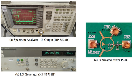
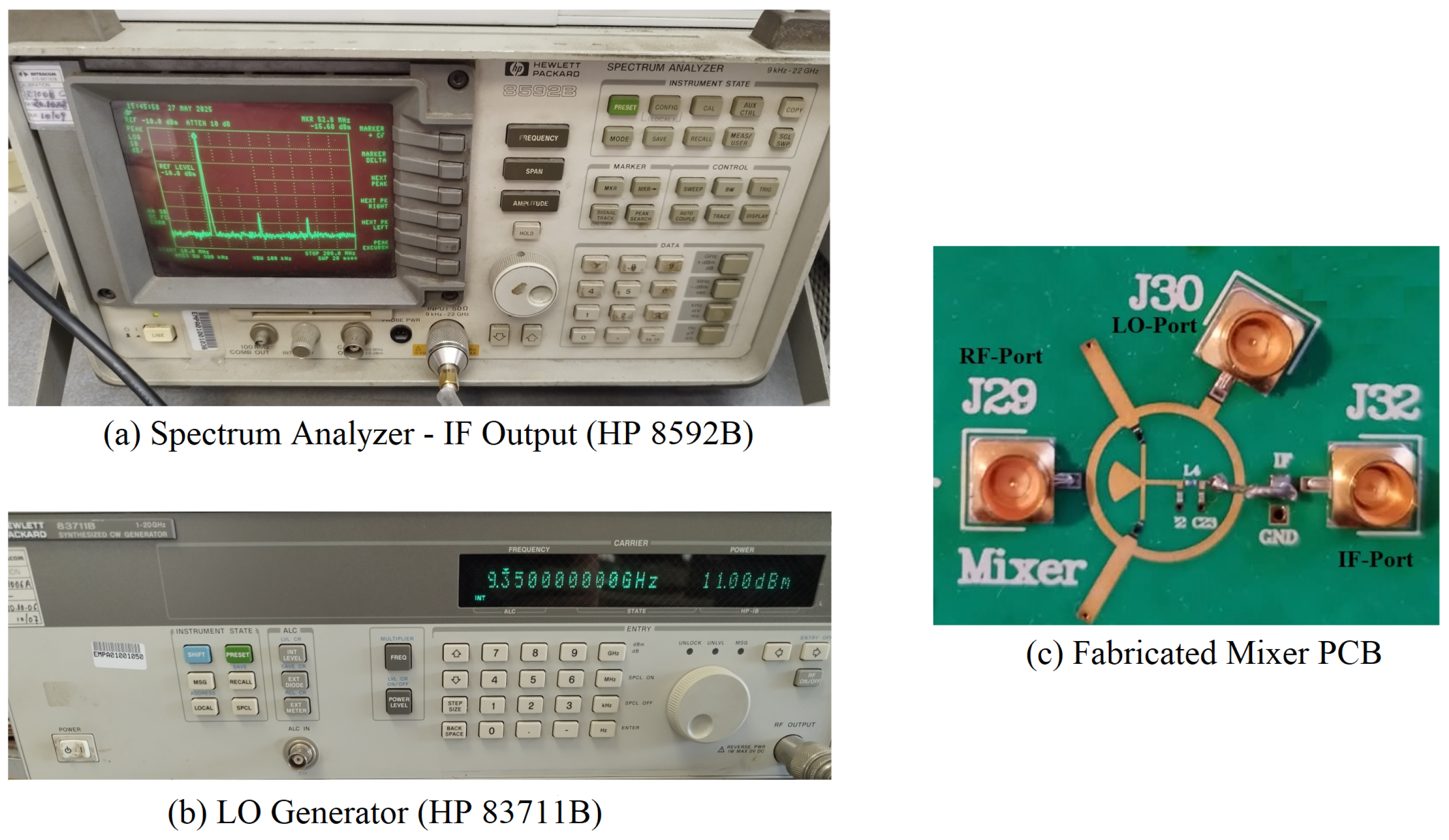
The experimental measurement procedure of the mixer is illustrated in Figure 28. The local oscillator (LO) frequency was set to 9.35 GHz, corresponding to the center of the X-band maritime radar allocation, while the RF excitation frequency was set to 9.4 and 10 GHz to evaluate the mixer performance under nominal and edge-of-band operating conditions. For selected RF frequencies and LO drive levels (11 and 20 dBm), the key performance metrics of the mixer, including conversion loss and the 1-dB compression point (), were extracted. In addition, second- and third-order mixing products (2IF and 3IF) were recorded to assess the spectral purity of the IF output.
Figure 28.
Measurement setup and fabricated PCB employed for the experimental characterization of the proposed passive mixer: (a) Spectrum analyzer monitoring the IF output (HP 8592B); (b) LO generator (HP 83711B); (c) fabricated PCB of the mixer indicating the RF, LO, and IF ports under measurement conditions.
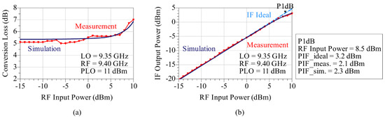
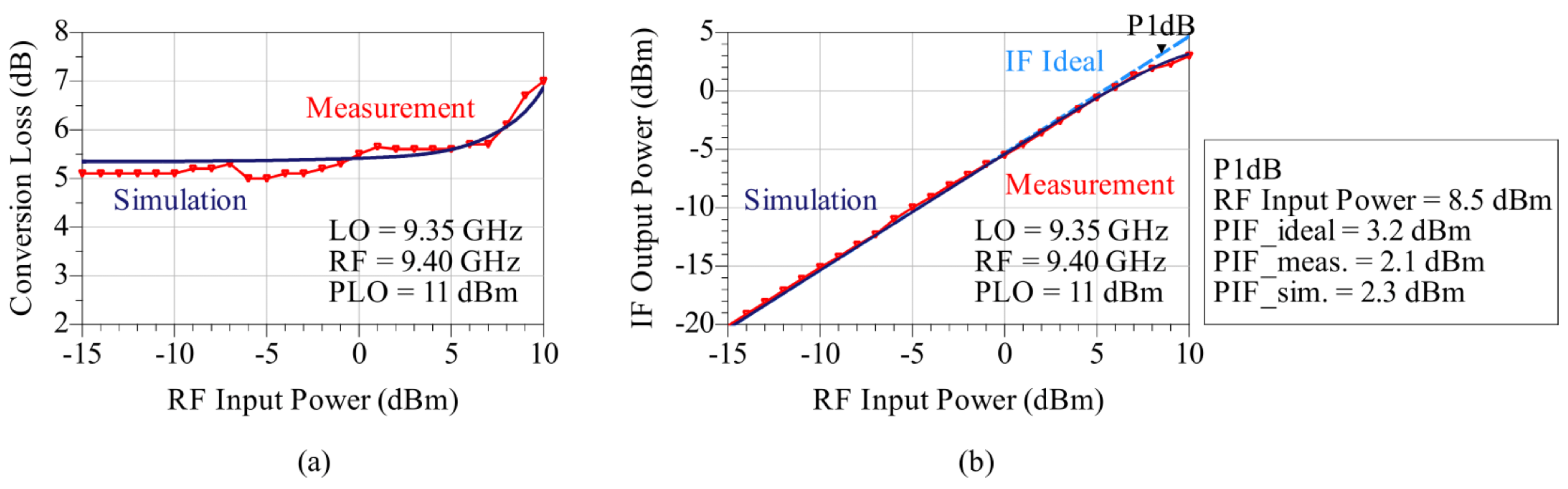
Figure 29 compares the simulated and measured conversion loss and 1-dB compression point () for an LO excitation at 9.35 GHz with a power level of 11 dBm and an RF input signal at 9.40 GHz. The conversion loss remains nearly constant in the linear operating region, with an average value below 5.5 dB, and increases as the RF input power rises and the mixer enters the nonlinear operating regime. The input-referred 1-dB compression point () is identified at approximately 8.5 dBm, in agreement with theoretical predictions.
Figure 29.
Comparison of simulated and measured results for the implemented mixer: (a) conversion loss and (b) input-referred 1-dB compression point (), for GHz, dBm, and GHz.
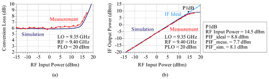
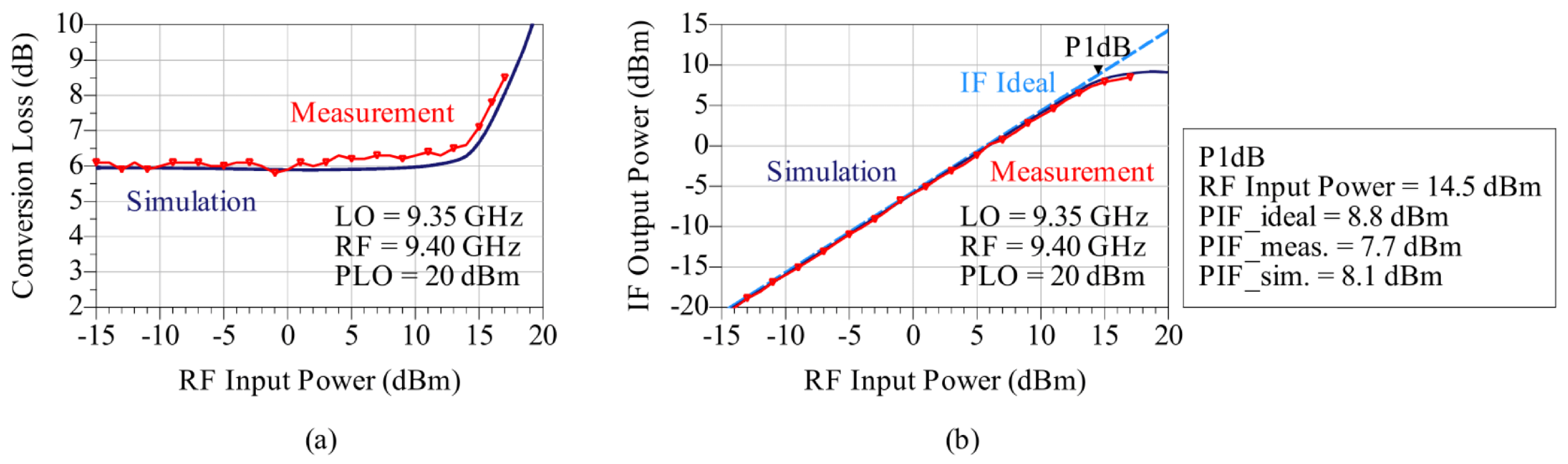
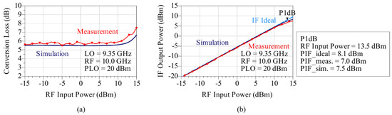
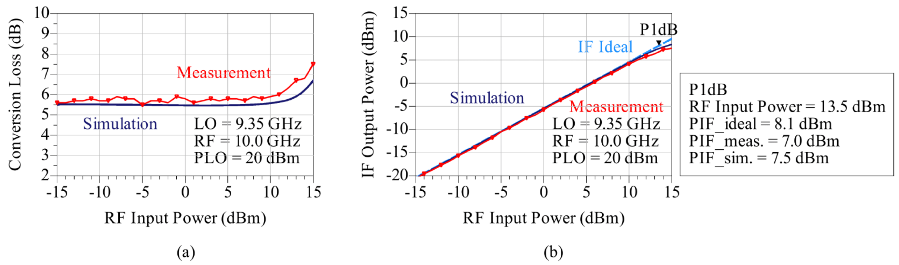
The LO excitation power was then increased to 20 dBm while maintaining the LO frequency at 9.35 GHz. The corresponding results for RF input frequencies of 9.4 and 10 GHz are shown in Figure 30 and Figure 31, respectively. The conversion loss remains approximately constant, at about 6 dB in the linear operating region, while the input-referred 1-dB compression point () shifts to approximately 14.5 dBm for GHz. This behavior indicates improved linearity with increasing LO drive level, consistent with the expected switching operation of the Schottky diodes.
Figure 30.
Comparison of simulated and measured results for the implemented mixer: (a) conversion loss and (b) input-referred 1-dB compression point (), for GHz, dBm, and GHz.
Figure 31.
Comparison of simulated and measured results for the implemented mixer: (a) conversion loss and (b) input-referred 1-dB compression point (), for GHz, dBm, and GHz.
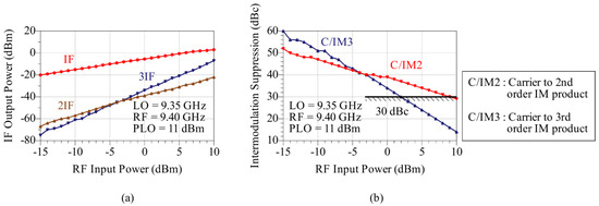
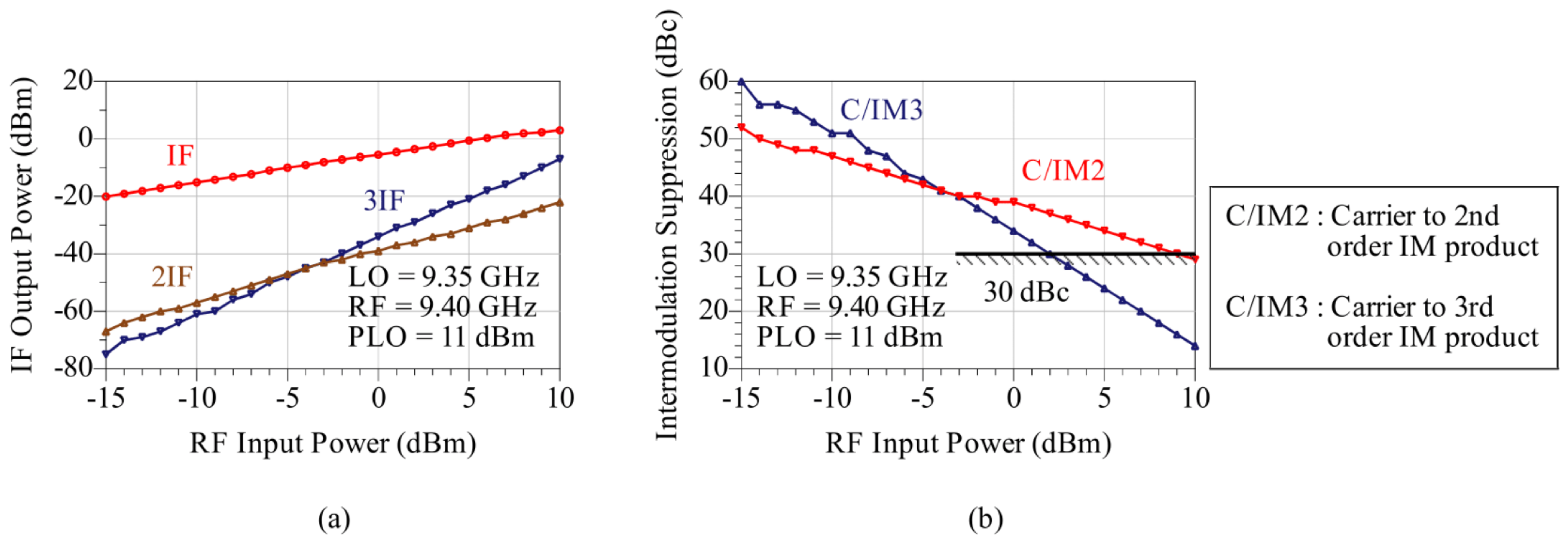
Figure 32 presents the spectral behavior of the IF output for an LO frequency of 9.35 GHz and a power level of 11 dBm, with an RF input at 9.40 GHz. Figure 32a shows the output power of the fundamental IF component together with the second- and third-order harmonics (2IF and 3IF), as a function of the RF input power. The fundamental component increases approximately linearly, while the harmonic components remain at significantly lower levels, indicating satisfactory spectral purity. As expected, the third-order component exhibits a steeper increase with RF input power, reflecting the nonlinear behavior of the mixing process.
Figure 32.
Spectral response of the mixer IF output for GHz, dBm, and GHz: (a) output power of the fundamental IF component and the second- and third-order harmonics (2IF and 3IF); (b) harmonic levels relative to the fundamental IF component, expressed in dBc.
Figure 32b presents the harmonic levels relative to the fundamental IF component, expressed in dBc. Across a wide portion of the examined RF input power range, the harmonic components remain more than 30 dBc below the fundamental IF tone, indicating satisfactory spectral purity at the mixer output. Although this analysis is conducted at an LO power level of 11 dBm, higher LO drive levels further improve linearity and harmonic suppression.
Overall, the experimental results confirm the proper operation of the implemented single-balanced passive mixer and validate the adopted design methodology. Good agreement between simulated and measured results is observed, verifying the predicted performance in terms of conversion loss, input-referred 1-dB compression point, and spectral purity at the IF output.
4.5. Overall Measured Performance Summary
Table 3 summarizes the measured and simulated performance of the proposed passive I/Q downconversion subsystem, encompassing both the individual building blocks and the resulting subsystem-level characteristics. The RF power divider and the hybrid coupler exhibit low insertion loss and well-controlled amplitude and phase imbalance, enabling accurate quadrature signal generation, while the single-balanced passive mixer demonstrates stable conversion behavior and adequate linearity. In addition to conventional RF metrics, the table consolidates key subsystem-level performance indicators, including I/Q imbalance, image rejection ratio, conversion loss, compression point, and spectral purity. Measured results are reported where available, particularly for mixer-related metrics, whereas circuit-level simulations are employed for port-to-port isolation.
Table 3.
Overall performance summary of the passive I/Q downconversion subsystem and the maritime radar allocation.
Regarding the subsystem-level I/Q metrics, the I/Q amplitude imbalance and phase error were obtained by combining the measured amplitude and phase imbalances of the RF power divider and the LO hybrid coupler. Based on these measured values, the corresponding image rejection ratios were computed for the complete I/Q subsystem. The proposed implementation achieves image rejection ratios exceeding 30 dB, reaching up to 33 dB, while maintaining I/Q amplitude imbalance within dB and phase error within . These results confirm effective image suppression and accurate quadrature signal generation across the X-band frequency range. The reported conversion loss corresponds to the mixer stage and remains approximately 6 dB, while the measured input-referred 1-dB compression point of approximately 14 dBm confirms sufficient linearity for the intended application. Performance further improves within the maritime radar allocation, where enhanced balance and increased image rejection are observed, confirming the suitability of the proposed architecture for broadband passive I/Q receiver operation.
5. Discussion in the Context of the State-of-the-Art
The objective of this work is the design and experimental validation of a passive I/Q downconversion subsystem, comprising an RF power divider, a hybrid coupler, and a passive mixer, rather than the realization of a complete receiver chain. Within this scope, emphasis is placed on achieving a well-balanced and low-complexity subsystem with minimal calibration requirements over the targeted X-band and maritime radar allocation. Direct comparison with prior work is not straightforward, since most reported designs either focus on individual building blocks or consider substantially different bandwidths and system configurations.
Table 4 compares the performance of the proposed coupled-line Wilkinson power divider in comparison with representative state-of-the-art implementations reported in the literature. The comparison indicates that the proposed divider achieves competitive performance in terms of phase and amplitude balance while maintaining high output-port isolation across the operating band. In particular, the obtained results demonstrate that the adopted coupled-line Wilkinson topology provides a favorable trade-off between electrical performance and implementation complexity. Moreover, while competitive performance is maintained across the entire X-band, improved balance characteristics are achieved within the targeted maritime radar sub-band. These results confirm the suitability of the proposed architecture for broadband X-band direct-conversion receiver applications, where accurate signal balance and low implementation complexity are important design requirements.
Table 4.
Performance comparison of the proposed coupled-line Wilkinson power divider with representative power divider implementations reported in the literature.
Broadband quadrature-generation networks are key components of direct-conversion receiver architectures, since their phase and amplitude characteristics directly influence I/Q matching and image-rejection performance. Table 5 compares the performance of the proposed broadband 90° hybrid coupler with representative implementations reported in the literature. The comparison indicates that the proposed architecture achieves competitive quadrature-generation performance across the operating band while maintaining a relatively simple implementation. These characteristics highlight the effectiveness of the proposed hybrid coupler for broadband I/Q signal generation and demonstrate its suitability for practical X-band direct-conversion receiver architectures.
Table 5.
Performance comparison of the proposed broadband 90° hybrid coupler with representative hybrid coupler implementations reported in the literature.
The mixer stage constitutes the most critical component in terms of linearity and overall subsystem performance. Table 6 compares the performance of the proposed passive mixer with representative passive mixer implementations reported in the literature. It should be noted that the referenced designs employ diverse semiconductor technologies, operating frequencies, and LO excitation levels; therefore, the comparison should be regarded as indicative rather than strictly equivalent. Within this context, the proposed design achieves competitive performance with respect to representative passive mixer implementations. In particular, the proposed architecture provides a favorable trade-off between conversion loss and linearity while maintaining a simple PCB-based implementation. These characteristics validate the adopted design approach and demonstrate the suitability of the proposed mixer for broadband X-band direct-conversion receiver applications.
Table 6.
Performance comparison of the proposed mixer with representative passive mixer implementations reported in the literature.
From a system-level perspective, the presented results demonstrate that a fully passive I/Q subsystem can achieve robust performance without active correction mechanisms. By combining carefully designed RF and LO distribution networks with a passive mixing stage, the implementation maintains controlled amplitude and phase balance across the operating band, directly supporting effective image suppression.
The measured performance of the individual building blocks, together with the corresponding state-of-the-art comparisons, validates the proposed design methodology and confirms the suitability of the proposed architecture for practical broadband X-band direct-conversion receiver implementations.
6. Conclusions
This paper presented the design, implementation, and experimental validation of a passive X-band I/Q downconversion subsystem intended for maritime radar applications. The proposed architecture combines an RF power divider, an LO 90° hybrid coupler, and a single-balanced passive mixer to realize quadrature signal generation for a direct-conversion receiver using a fully passive microstrip implementation on a two-layer Rogers RO4350B substrate.
The experimental results demonstrated accurate I/Q signal generation across the X-band frequency range. By combining the measured amplitude and phase imbalances of the RF power divider and the LO 90° hybrid coupler, the complete subsystem achieved an amplitude imbalance within dB and a phase error within , resulting in image rejection ratios exceeding 30 dB across the X-band frequency range. These results confirm effective image suppression and accurate quadrature signal generation without the need for active calibration techniques.
The proposed single-balanced passive mixer exhibited a conversion loss of approximately 6 dB while maintaining an input-referred 1-dB compression point of up to 14.5 dBm. Furthermore, the use of a radial stub at the IF node was shown to improve the RF/LO termination conditions and provide a more favorable impedance environment at the diode output node compared to a conventional bypass-capacitor implementation.
The best performance was obtained within the maritime radar allocation (9.2–9.5 GHz), where the subsystem exhibited improved amplitude and phase balance, enhanced image rejection reaching approximately 33 dB, and an increased input-referred 1-dB compression point. These results further validate the suitability of the proposed architecture for X-band maritime radar receiver applications. Overall, the obtained results demonstrate that high-quality passive I/Q signal generation can be achieved using a low-complexity architecture, providing a practical balance between image rejection, input-referred 1-dB compression point, insertion loss, and implementation cost.
Future work will focus on the integration of the proposed subsystem into a complete direct-conversion receiver, including front-end amplification, bandpass filtering, and baseband signal processing.
Author Contributions
T.B.: Conceptualization; methodology; formal analysis; investigation; data curation; visualization; writing—original draft preparation. Y.E.S.: investigation; resources; methodology; writing—review and editing. D.K.: supervision; writing—review and editing. I.P.: supervision; writing—review and editing. All authors have read and agreed to the published version of the manuscript.
Funding
This research received no external funding.
Institutional Review Board Statement
Not applicable.
Informed Consent Statement
Not applicable.
Data Availability Statement
Data are contained within the article.
Acknowledgments
The authors would like to thank Y. Stratakos for providing access to specialized measurement facilities and for their valuable technical support during the experimental validation. The authors also acknowledge the late Evangelia Karagianni for her guidance and support during the first author’s PhD studies.
Conflicts of Interest
The author Dr. Yorgos E. Stratakos is employed by the RMDS PC company. The remaining authors declare that the research is conducted in the absence of any commercial or financial relationships that could be construed as a potential conflict of interest.
References
- Griffiths, H.D.; Cohen, L.; Watts, S.; Mokole, E.L.; Baker, C.J.; Wicks, M.C.; Blunt, S.D. Radar Spectrum Engineering and Management: Technical and Regulatory Issues. Proc. IEEE 2015, 103, 85–102. [Google Scholar] [CrossRef] [Scilit]
- Cadence. Using the X-Band and Ka-Band Frequencies for Radar Applications. Cadence PCB Design Blog, 2023. Available online: https://resources.pcb.cadence.com/blog/2023-using-the-x-band-and-ka-band-frequencies-for-radar-applications (accessed on 17 November 2025).
- Bazzi, A.; Gast, F.; Liu, F.; Jin, S.; Fettweis, G.; Chafii, M. From Coverage to Sensing: ISAC Meets FR3. arXiv 2026, arXiv:2605.18120. [Google Scholar]
- Lund, B.; Graber, H.C.; Romeiser, R. Wind Retrieval from Shipborne Nautical X-Band Radar Data. IEEE Trans. Geosci. Remote Sens. 2012, 50, 3800–3811. [Google Scholar] [CrossRef] [Scilit]
- Dankert, H.; Horstmann, J.; Rosenthal, W. Ocean wind fields retrieved from radar-image sequences. J. Geophys. Res. Ocean. 2003, 108, 3352. [Google Scholar] [CrossRef] [Scilit]
- Young, I.R.; Rosenthal, W.; Ziemer, F. A three-dimensional analysis of marine radar images for the determination of ocean wave directionality and surface currents. J. Geophys. Res. Ocean. 1985, 90, 1049–1059. [Google Scholar] [CrossRef] [Scilit]
- Lund, B.; Graber, H.C.; Xue, J.; Romeiser, R. Analysis of internal wave signatures in marine radar data. IEEE Trans. Geosci. Remote Sens. 2013, 51, 4840–4852. [Google Scholar] [CrossRef] [Scilit]
- Nieto-Borge, J.C.; Hessner, K.; Jarabo-Amores, P.; de la Mata-Moya, D. Signal-to-noise ratio analysis to estimate ocean wave heights from X-band marine radar image time series. IET Radar Sonar Navig. 2008, 2, 35–41. [Google Scholar] [CrossRef] [Scilit]
- Nieto-Borge, J.C.; Guedes-Soares, C. Analysis of directional wave fields using X-band navigation radar. Coast. Eng. 2000, 40, 375–391. [Google Scholar] [CrossRef] [Scilit]
- Gangeskar, R. Ocean current estimated from X-band radar sea surface, images. IEEE Trans. Geosci. Remote Sens. 2002, 40, 783–792. [Google Scholar] [CrossRef]
- Senet, C.M.; Seemann, J.; Ziemer, F. The near-surface current velocity determined from image sequences of the sea surface. IEEE Trans. Geosci. Remote Sens. 2001, 39, 492–505. [Google Scholar] [CrossRef] [Scilit]
- Shen, C.; Huang, W.; Gill, E.W.; Carrasco, R.; Horstmann, J. An algorithm for surface current retrieval from X-band marine radar images. Remote Sens. 2015, 7, 7753–7767. [Google Scholar] [CrossRef] [Scilit]
- Horstmann, J.; Nieto-Borge, J.C.; Seemann, J.; Carrasco, R.; Lund, B. Wind, wave, and current retrieval utilizing X-band marine radars. In Coastal Ocean Observing Systems; Liu, Y., Kerkering, H., Weisberg, R.H., Eds.; Academic Press: Cambridge, MA, USA, 2015; Chapter 16; pp. 281–304. [Google Scholar] [CrossRef] [Scilit]
- Huang, W.; Liu, X.; Gill, E.W. Ocean wind and wave measurements using X-band marine radar: A comprehensive review. Remote Sens. 2017, 9, 1261. [Google Scholar] [CrossRef] [Scilit]
- Vivone, G.; Braca, P. Joint probabilistic data association tracker for extended target tracking applied to X-band marine radar data. IEEE J. Ocean. Eng. 2016, 41, 1007–1019. [Google Scholar] [CrossRef] [Scilit]
- Zhu, X.; Li, Y.; Feng, H.; Liu, B.; Xu, J. Oil spill detection method using X-band marine radar imagery. J. Appl. Remote Sens. 2015, 9, 095985. [Google Scholar] [CrossRef] [Scilit]
- Dankert, H.; Horstmann, J.; Lehner, S.; Rosenthal, W. Detection of Wave Groups in SAR Images and Radar Image Sequences. IEEE Trans. Geosci. Remote Sens. 2003, 41, 1437–1446. [Google Scholar] [CrossRef]
- Chen, Z.; Pan, J.; He, Y.; Devlin, A.T. Estimate of Tidal Constituents in Nearshore Waters Using X-Band Marine Radar Image Sequences. IEEE Trans. Geosci. Remote Sens. 2016, 54, 6700–6711. [Google Scholar] [CrossRef] [Scilit]
- Bell, P.S.; Osler, J.C. Mapping Bathymetry Using X-Band Marine Radar Data Recorded from a Moving Vessel. Ocean Dyn. 2011, 61, 2141–2156. [Google Scholar] [CrossRef] [Scilit]
- Wu, L.C.; Doong, D.J.; Wang, J.H. Bathymetry Determination from Marine Radar Image Sequences Using the Hilbert Transform. IEEE Geosci. Remote Sens. Lett. 2017, 14, 644–648. [Google Scholar] [CrossRef] [Scilit]
- Punzo, M.; Lanciano, C.; Tarallo, D.; Bianco, F.; Cavuoto, G.; De Rosa, R.; Di Fiore, V.; Cianflone, G.; Dominici, R.; Iavarone, M. Application of X-Band Wave Radar for Coastal Dynamic Analysis: Case Test of Bagnara Calabra (South Tyrrhenian Sea, Italy). J. Sens. 2016, 2016, 6236925. [Google Scholar] [CrossRef] [Scilit]
- Zheng, H. Designing a High Performance 4–12 GHz Direct Conversion Receiver with LMX8410L IQ Demodulator; Application Report SNAA329; Texas Instruments: Dallas, TX, USA, 2019. [Google Scholar]
- Wu, Y.; Liu, Y.; Xue, Q. An Analytical Approach for a Novel Coupled-Line Dual-Band Wilkinson Power Divider. IEEE Trans. Microw. Theory Tech. 2011, 59, 286–294. [Google Scholar] [CrossRef] [Scilit]
- Sun, R.; Chen, Q.; Han, R.; Lu, Z. Analysis and Design of Wideband 90° Microstrip Hybrid Coupler. IEEE Access 2019, 7, 186409–186416. [Google Scholar] [CrossRef] [Scilit]
- Lin, Y.S.; Lan, K.S. Spiral-Coupled-Line-Based Wilkinson Power Divider. IEEE Microw. Wirel. Compon. Lett. 2021, 31, 241–244. [Google Scholar] [CrossRef] [Scilit]
- Eom, D.S.; Byun, J.; Lee, H.Y. Multilayer Substrate Integrated Waveguide Four-Way Out-of-Phase Power Divider. IEEE Trans. Microw. Theory Tech. 2009, 57, 3469–3476. [Google Scholar] [CrossRef] [Scilit]
- Djerafi, T.; Hammou, D.; Wu, K.; Tatu, S.O. Ring-Shaped Substrate Integrated Waveguide Wilkinson Power Dividers/Combiners. IEEE Trans. Compon. Packag. Manuf. Technol. 2014, 4, 1461–1469. [Google Scholar] [CrossRef] [Scilit]
- Pasian, M.; Silvestri, L.; Rave, C.; Bozzi, M.; Perregrini, L.; Jacob, A.F.; Samanta, K.K. Substrate-Integrated-Waveguide E-Plane 3-dB Power-Divider/Combiner Based on Resistive Layers. IEEE Trans. Microw. Theory Tech. 2017, 65, 1498–1510. [Google Scholar] [CrossRef] [Scilit]
- Huang, Y.M.; Jiang, W.; Jin, H.; Zhou, Y.; Leng, S.; Wang, G.; Wu, K. Substrate-Integrated Waveguide Power Combiner/Divider Incorporating Absorbing Material. IEEE Microw. Wirel. Compon. Lett. 2017, 27, 885–887. [Google Scholar] [CrossRef] [Scilit]
- Zhou, Y.; Huang, Y.M.; Jin, H.; Ding, S.; Xu, D.; Silvestri, L.; Bozzi, M.; Perregrini, L. Slow-Wave Half-Mode Substrate Integrated Waveguide 3-dB Wilkinson Power Divider/Combiner Incorporating Nonperiodic Patterning. IEEE Microw. Wirel. Compon. Lett. 2018, 28, 765–767. [Google Scholar] [CrossRef] [Scilit]
- Luo, Q.; Zhou, J.; Luo, X. Compact Fully-Packaged Hybrid CPWG/SIDGS for 1-to-4 In-Phase/Out-of-Phase Power Splitter With Low Amplitude/Phase Imbalances, Low Radiation Loss, and Good Isolation. IEEE Access 2025, 13, 57442–57454. [Google Scholar] [CrossRef] [Scilit]
- Pozar, D.M. Microwave Engineering, 4th ed.; John Wiley & Sons: Hoboken, NJ, USA, 2012. [Google Scholar]
- Tang, C.W.; Chen, M.G.; Lin, Y.S.; Wu, J.W. Broadband microstrip branch-line coupler with defected ground structure. Electron. Lett. 2006, 42, 1458–1460. [Google Scholar] [CrossRef] [Scilit]
- Chun, Y.H.; Hong, J.S. Compact wide-band branch-line hybrids. IEEE Trans. Microw. Theory Tech. 2006, 54, 704–709. [Google Scholar] [CrossRef] [Scilit]
- Yoon, H.J.; Min, B.W. Two Section Wideband 90° Hybrid Coupler Using Parallel-Coupled Three-Line. IEEE Microw. Wirel. Compon. Lett. 2017, 27, 548–550. [Google Scholar] [CrossRef] [Scilit]
- Zaidel, D.N.A.; Rahim, S.K.A.; Neman, N.; Chew, C.L.; Khamis, N.H. A Design of Octagon-Shaped 3-dB Ultra Wideband Coupler Using Multilayer Technology. Microw. Opt. Technol. Lett. 2013, 55, 127–130. [Google Scholar] [CrossRef] [Scilit]
- Nedil, M.; Talbi, L.; Denidni, T.A. Design of a New Directional Coupler Using CPW Multilayer Technology. Microw. Opt. Technol. Lett. 2006, 48, 471–474. [Google Scholar] [CrossRef] [Scilit]
- Osmani, R. Synthesis of Lange Couplers. IEEE Trans. Microw. Theory Tech. 1981, 29, 168–170. [Google Scholar] [CrossRef] [Scilit]
- Janisz, K.; Smolarz, R.; Rydosz, A.; Wincza, K.; Gruszczynski, S. Compensated 3-dB lange directional coupler in suspended microstrip technique. In Proceedings of the 2017 7th IEEE International Symposium on Microwave, Antenna, Propagation, and EMC Technologies (MAPE), Xi’an, China, 24–27 October 2017; pp. 288–291. [Google Scholar] [CrossRef] [Scilit]
- Wu, Y.; Liu, Q.; Shen, J.; Liu, Y. A novel wide-band hybrid coupler using coupled-line power divider and improved coupled-line phase shifter. J. Electromagn. Waves Appl. 2013, 27, 374–384. [Google Scholar] [CrossRef] [Scilit]
- Schiffman, B. A New Class of Broad-Band Microwave 90-Degree Phase Shifters. IRE Trans. Microw. Theory Tech. 1958, 6, 232–237. [Google Scholar] [CrossRef] [Scilit]
- Quirarte, J.; Starski, J. Novel Schiffman phase shifters. IEEE Trans. Microw. Theory Tech. 1993, 41, 9–14. [Google Scholar] [CrossRef] [Scilit]
- Guo, Y.X.; Zhang, Z.Y.; Ong, L.C. Improved wide-band Schiffman phase shifter. IEEE Trans. Microw. Theory Tech. 2006, 54, 1196–1200. [Google Scholar] [CrossRef] [Scilit]
- Jafari, E.; Hodjat-Kashani, F.; Rezaiesarlak, R. A Broadband Quadrature Hybrid Using Improved Wideband Schiffman Phase Shifter. Prog. Electromagn. Res. C 2009, 11, 229–236. [Google Scholar] [CrossRef] [Scilit]
- Zhang, T.; Du, J.; Guo, Y.J. An 8–10-GHz Low-Loss Image-Reject HTS Mixer Based on Cascaded Josephson Junctions. IEEE Microw. Wirel. Compon. Lett. 2021, 31, 945–948. [Google Scholar] [CrossRef] [Scilit]
- Ahmed, A.; Rebeiz, G.M. An 8–30 GHz High-Linearity Harmonic-Rejection Mixer in 45 nm CMOS SOI. IEEE Trans. Microw. Theory Tech. 2024, 72, 3361–3372. [Google Scholar] [CrossRef] [Scilit]
- Hassan, O.; Ahmed, A.; Rebeiz, G.M. A 7–20 GHz Ultra-High-Linearity Passive Mixer in 45 nm CMOS SOI. IEEE J. Solid-State Circuits 2025, 60, 1607–1618. [Google Scholar] [CrossRef] [Scilit]
- Gong, T.; Cheng, Z.; Le, C.; Xuan, X.; Zheng, B.; Zhang, Z.; Jia, M. A Broadband Low Conversion Loss Single-Ended Resistive Mixer With an Innovative Topology. IEEE Microw. Wirel. Technol. Lett. 2024, 34, 1103–1106. [Google Scholar] [CrossRef] [Scilit]
- Zhang, Y.; Zhuang, Y.; Zhang, H.; Yang, L.; Wang, J.; Zhang, C.; Guo, Y. An 8–26 GHz Passive Mixer with Excellent Port Matching Utilizing Marchand Balun and Capacitor Compensation. Chin. J. Electron. 2025, 34, 422–428. [Google Scholar] [CrossRef] [Scilit]
- Pal, R.; Mandal, M.K. A Wideband Subharmonic Image-Reject Mixer With a Fixed IF Using Schottky Diodes. IEEE J. Microwaves 2025, 5, 996–1002. [Google Scholar] [CrossRef] [Scilit]
- Razavi, B. RF Microelectronics, 2nd ed.; Prentice Hall: Hoboken, NJ, USA, 2012. [Google Scholar]
- Han, R.C.; Sun, R.Y.; Shi, S.H. A wideband planar hybrid coupler using coupled-line power divider and broadband phase shifter. In Proceedings of the 2017 Sixth Asia-Pacific Conference on Antennas and Propagation (APCAP), Xi’an, China, 16–19 October 2017; pp. 1–3. [Google Scholar] [CrossRef] [Scilit]
- Chen, Q.; Chen, X.; Cai, H.; Chen, F. Schottky Diode Large-Signal Equivalent-Circuit Parameters Extraction for High-Efficiency Microwave Rectifying Circuit Design. IEEE Trans. Circuits Syst. II Express Briefs 2020, 67, 2722–2726. [Google Scholar] [CrossRef] [Scilit]

Disclaimer/Publisher’s Note: The statements, opinions and data contained in all publications are solely those of the individual author(s) and contributor(s) and not of MDPI and/or the editor(s). MDPI and/or the editor(s) disclaim responsibility for any injury to people or property resulting from any ideas, methods, instructions or products referred to in the content. |
© 2026 by the authors. Licensee MDPI, Basel, Switzerland. This article is an open access article distributed under the terms and conditions of the Creative Commons Attribution (CC BY) license.