


Abstract
This article presents the design and analysis of a three-way wideband Wilkinson power divider using a lump-type transmission line circuit instead of quarter-wave transmission lines, and a two-section cascaded lumped transmission line circuit technique instead of a single-section lumped transmission line to improve bandwidth efficiency. The proposed circuit is analyzed using even-mode and odd-mode techniques to find the synthesized parameters. Due to the design challenges in X-band applications, parasitic capacitors play a crucial role in layout design. This work presents a parasitic extraction method using the Y-parameter to analyze the layout of each input/output port. The layout is designed to be compact at (0.03λ0 × 0.03λ0) on 0.12 um GaN on SiC Technology. The resulting measurement yields a −10 dB fractional bandwidth of 80.39%, while the amplitude and phase balance are 0.1 dB and 5.8° (−13 dB fractional bandwidth of 52.4%, while the amplitude and phase balance are 0.04 dB and 4.9°). Overall, the circuit is compact and provides good performance for X-band frequency applications.
1. Introduction
Power dividers are used in parts of many RF circuits, such as power amplifiers and low-noise amplifiers. In current applications, many RF blocks are implemented on-chip. Therefore, the use of on-chip power dividers is more convenient.
In this work, a power divider for the X-band frequency range supporting wideband applications was designed. Although there have been many research reports on 2-way Wilkinson power dividers, L. Wang et al. found that using a cascaded 2-way Wilkinson power divider resulted in power loss, increased reflection, and increased space requirements [1]. Therefore, S. Cheng and M. Pavlick presented an N-way Wilkinson power divider, which allows for the study of Wilkinson power dividers with a larger number of output ports [2]. However, since Wilkinson power dividers generally have a relatively large circuit area, several research papers have focused on reducing the size of the transmission line of the Wilkinson power divider by using the lumped transmission line technique, which uses inductor, capacitor, and resistor devices connected in various networks [3,4,5]. However, using lumped transmission lines instead of quarter-wave transmission lines still does not provide sufficient bandwidth efficiency, leading to the use of multi-section lumped transmission lines to expand bandwidth [6,7,8,9]. Despite extensive research on power dividers, the demand for three-way power dividers continues to grow. Currently, research on on-chip three-way power dividers is relatively limited.
Although several on-chip Wilkinson power dividers (WPDs) have been reported, most architectures focus on 2-way splits [3,7,8] or 4-way splits [9,10]. Cascading standard 2-way dividers to feed odd-numbered array channels leads to asymmetric layouts, larger chip areas, and additional insertion losses. On the other hand, existing 3-way dividers, such as [11], rely on a single-section lumped λ/4 replacement using LTCC technology, which offers limited operating bandwidth and suffers from performance degradation due to parasitic losses when translated to semiconductor substrates.
In this work, we propose a novel compact 3-way power divider monolithically integrated on a GaN process. To overcome the bandwidth limitations of traditional single-section designs [11] and mitigate GaN substrate losses, a two-stage cascaded lumped-element network is implemented. This topology achieves a significantly broader bandwidth while maintaining a compact chip footprint suitable for on-chip integration.
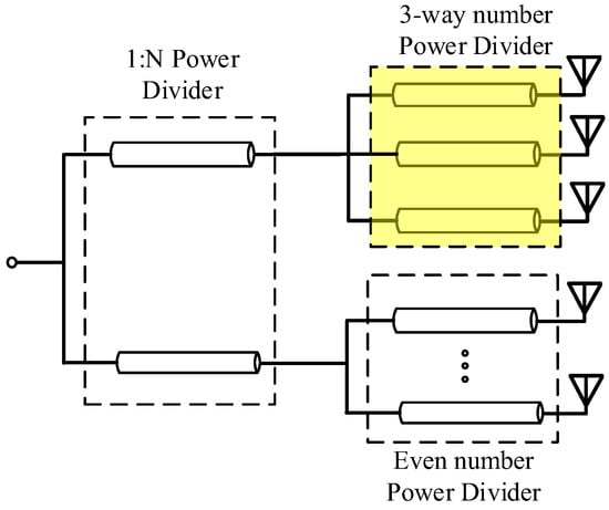
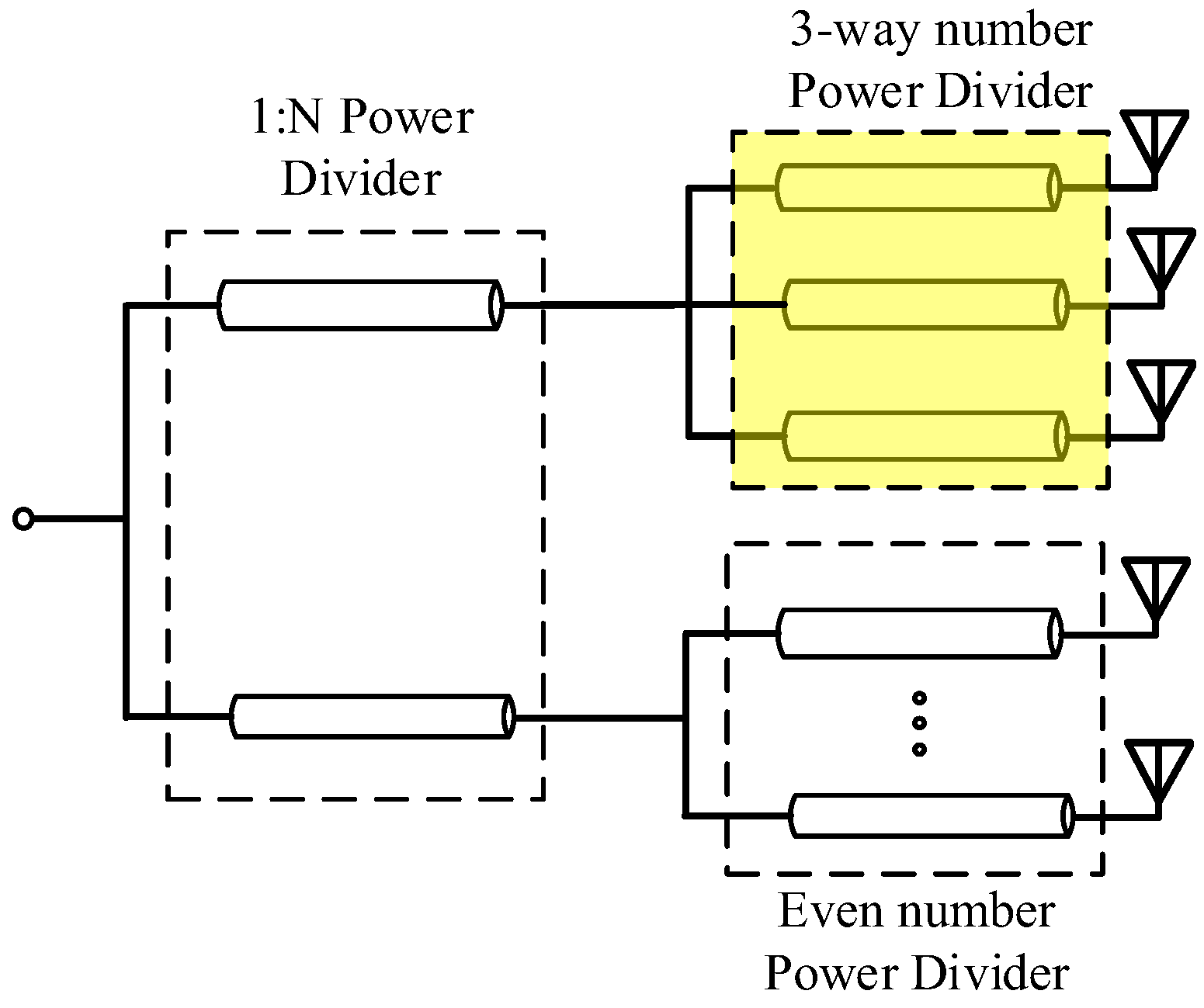
The three-way power divider can be used for applications such as distributing power for an odd number of elements in an antenna array. By using an even number of 1:N power divider with a single 3-way power divider, an odd-way power divider can be formed. Figure 1 shows the system. This paper is aimed at developing a 3-way power divider for the wide X-band.
Figure 1.
An odd-number power divider system.
2. Lumped Transmission Line Circuit
2.1. Design with Lumped Transmission Line
Research designs to increase the bandwidth of Wilkinson Power Divider (WPD) circuits typically rely on quarter-wave transmission lines. However, the relatively large physical size of distributed transmission lines makes them less suitable for integrated circuits (ICs). Therefore, lumped-element transmission lines have been investigated as an alternative for implementing compact on-chip WPDs [12,13,14]. In these approaches, conventional transmission lines are replaced by equivalent lumped-element networks, such as π-type structures consisting of series inductors and shunt capacitors [13]. Lumped-element transmission lines have also been employed to achieve wideband WPDs in CMOS technology [14]. The lumped transmission line structure used in this work is constructed from series inductors and shunt capacitors, as shown in Figure 2.
Figure 2.
A distributed transmission line is represented by an equivalent lumped-element circuit, where a lumped π-network is employed to model the electrical behavior of the distributed transmission line.
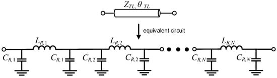
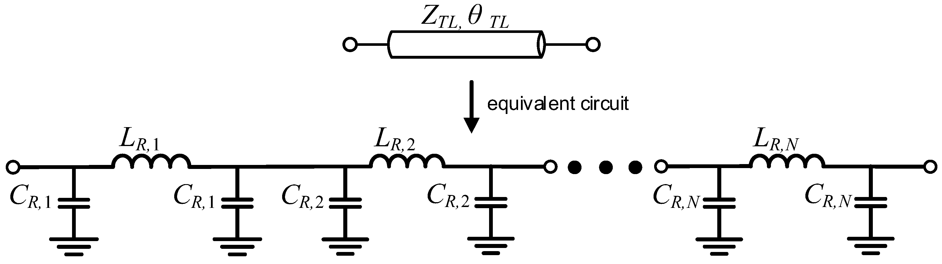
This right-handed lumped transmission line structure can mimic the behavior of a distributed transmission line; however, its continuously varying impedance with frequency results in a relatively narrow bandwidth. The values of the lumped transmission-line components can be calculated using the equations reported in [15]. To improve bandwidth and provide greater design flexibility, two-section Wilkinson power dividers have been investigated [8], while lumped-element and π-type structures have been employed to replace conventional quarter-wavelength transmission lines for circuit miniaturization and wideband operation [16]. Furthermore, multi-section lumped-element structures using cascaded LC π-networks have been demonstrated to approximate a quarter-wavelength transmission line and achieve wideband operation [17,18]. In this work, the transmission line is divided into cascaded sections with shorter electrical lengths to form an equivalent distributed transmission line, as shown in Figure 3.
Figure 3.
Equivalent cascaded lumped-element circuit representation of a distributed transmission line.
2.2. Loss Study of Lumped Transmission Line Circuit
A cascaded lumped transmission line circuit can be used to maintain characteristic impedance over a range of frequencies. This section investigates the impedance and phase deviations from those of an ideal distributed transmission line. In this work, identical transmission line sections are cascaded to form the overall lumped transmission line. The ABCD matrix approach can be used to characterize the electrical behavior of each lumped transmission line section and the cascaded structure [18]. Accordingly, the ABCD matrix of the cascaded transmission line can be obtained from the ABCD matrix of a single lumped transmission-line section, , as follows:
where , , are the electrical length, the characteristic impedance and the ABCD matrix of each transmission line section and is the ABCD matrix of the cascaded line. The characteristic impedance of the cascaded line can be found from the total ABCD matrix as follows:
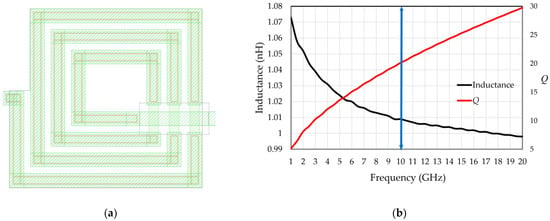
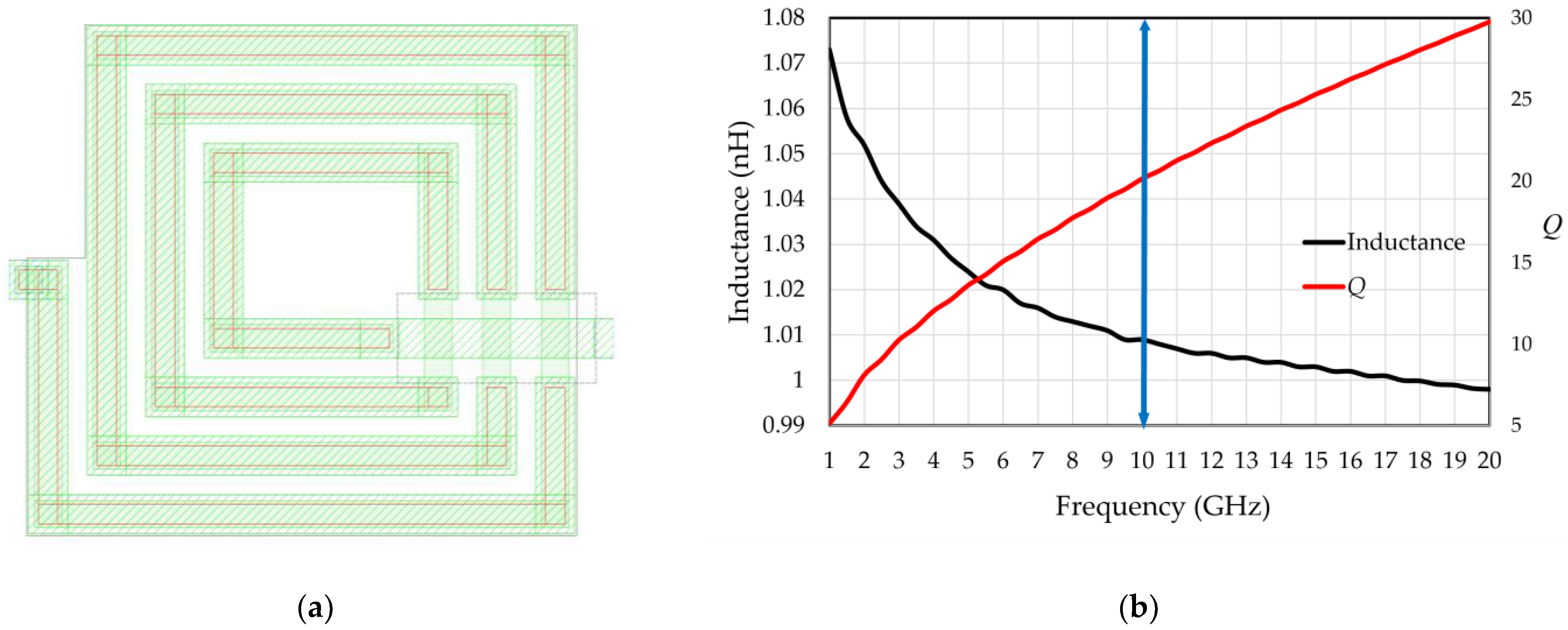
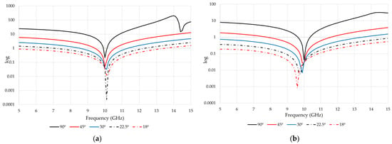
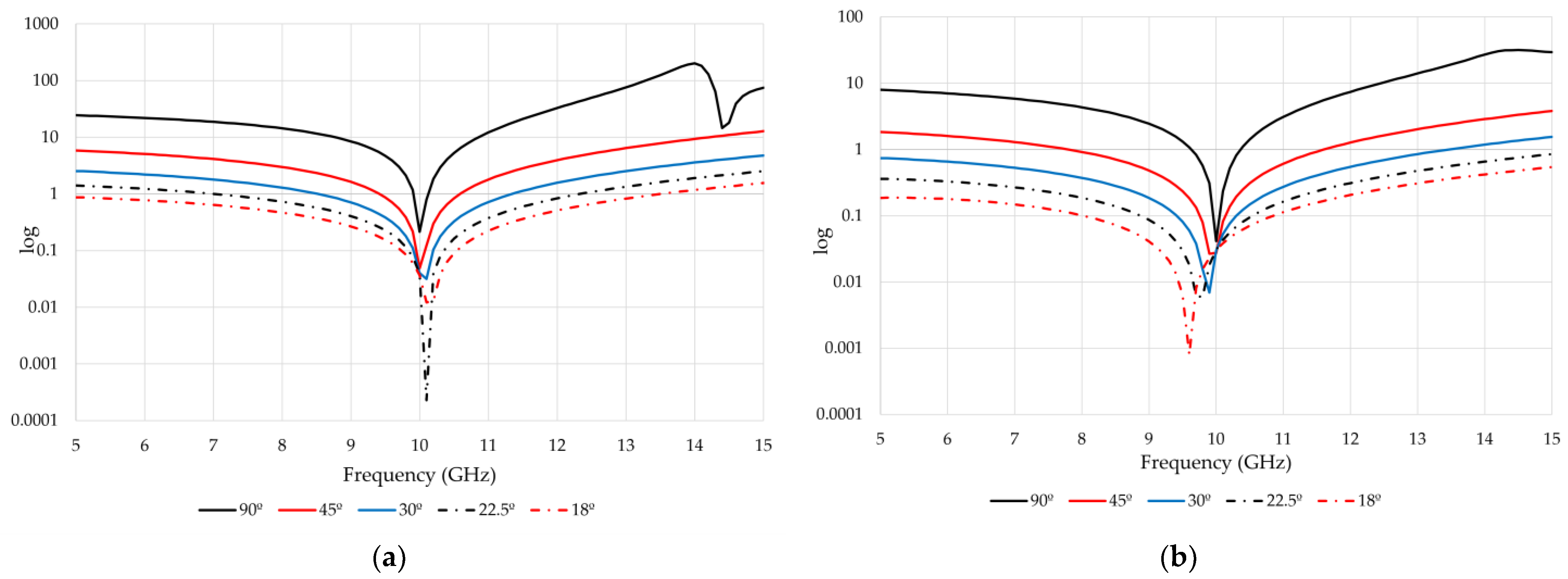
Since lumped element devices in the form of a π-network are lossy in general, their quality factor (Q) must be considered in the design, especially the quality factor of the inductors. The Q-factor of an integrated inductor depends on its layout, conductor and substrate losses, and fabrication process [19,20]. In this work, the chip was implemented on the GaN process. Therefore, the Q-factor was evaluated based on the implemented inductor rather than assuming a general Q-factor range. To evaluate the quality factor (Q) of the inductor, a 1 nH spiral inductor is utilized in the dividercircuit. Figure 4 illustrates its physical layout, inductance, and Q-factor curve. As observed from the figure, the inductor achieves a Q-factor of 19.45 at 10 GHz. Therefore, in the following simulation study, the inductor is set to have a Q value of 20. Multi-section transmission lines using lossy inductors are formed to have an overall electrical length of 90° and a characteristic impedance of at 10 GHz. The lines in the simulation are of different subsections, e.g., electrical lengths of 90°, 45°, 30°, 22.5°, and 18°. Their behaviors are compared with those of a theoretical 90° transmission line over 5–15 GHz. The percentage errors in the characteristic impedance and the electrical length are shown in Figure 5. Note that denotes the port impedance, which is 50 Ω in this work.
Figure 4.
Simulation study of a 1 nH inductor. (a) layout of the inductor (b) inductance and Q-factor curves.
Figure 5.
Theoretical simulation results of comparison of the percentage error of (a) characteristic impedance () and (b) electrical length () for cascaded lumped transmission line circuits with sub-section.
3. Even and Odd Mode Analysis of WPD Circuits
3.1. Conventional Lumped Circuit Transmission Line WPD
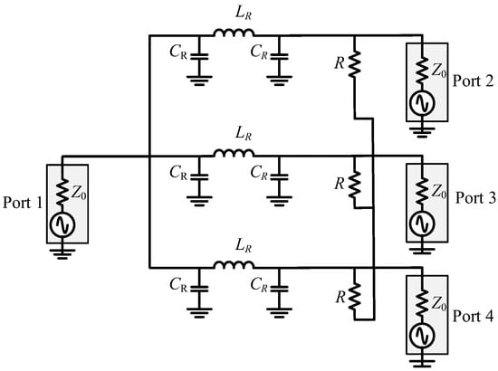
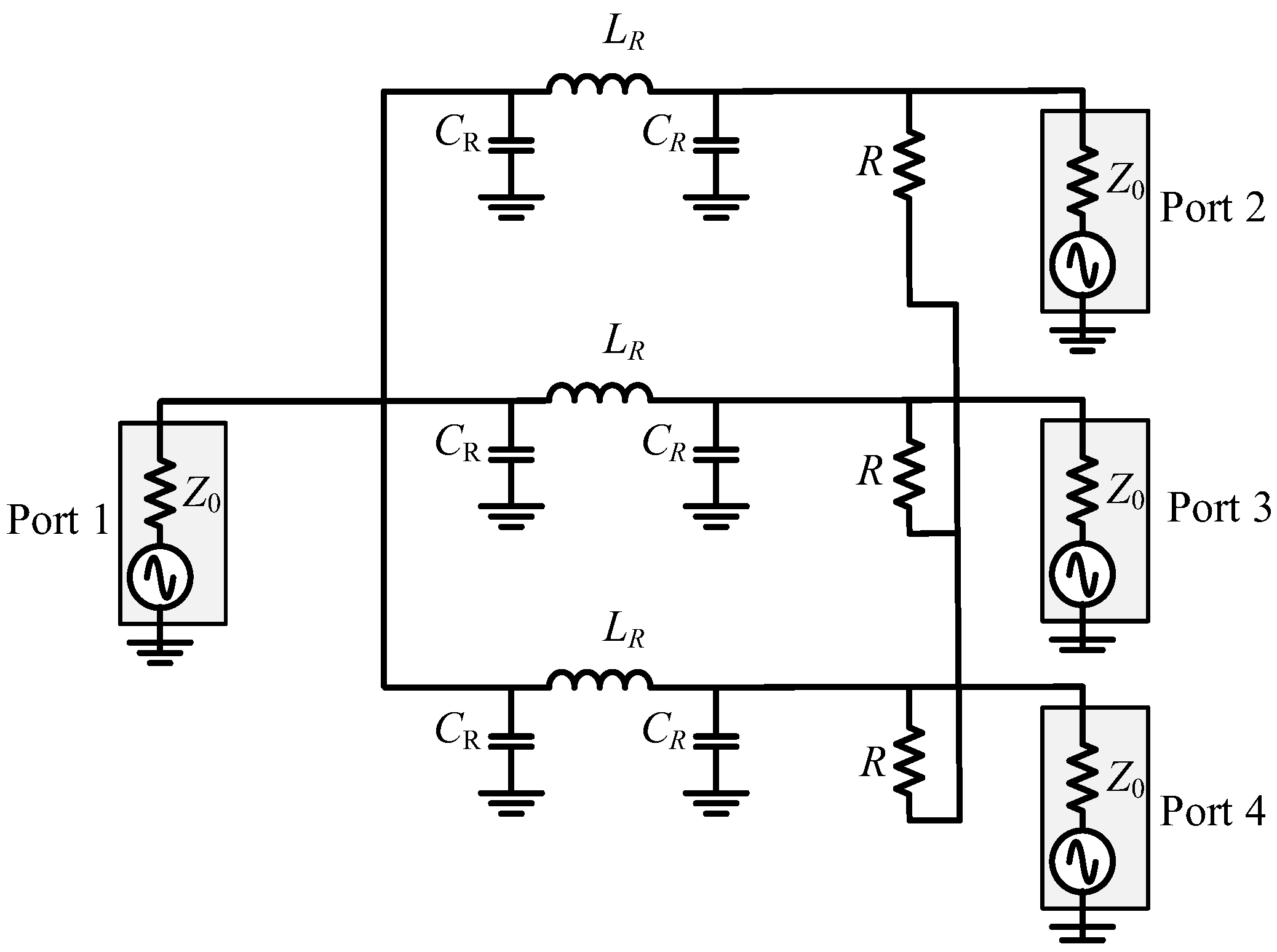
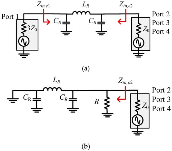
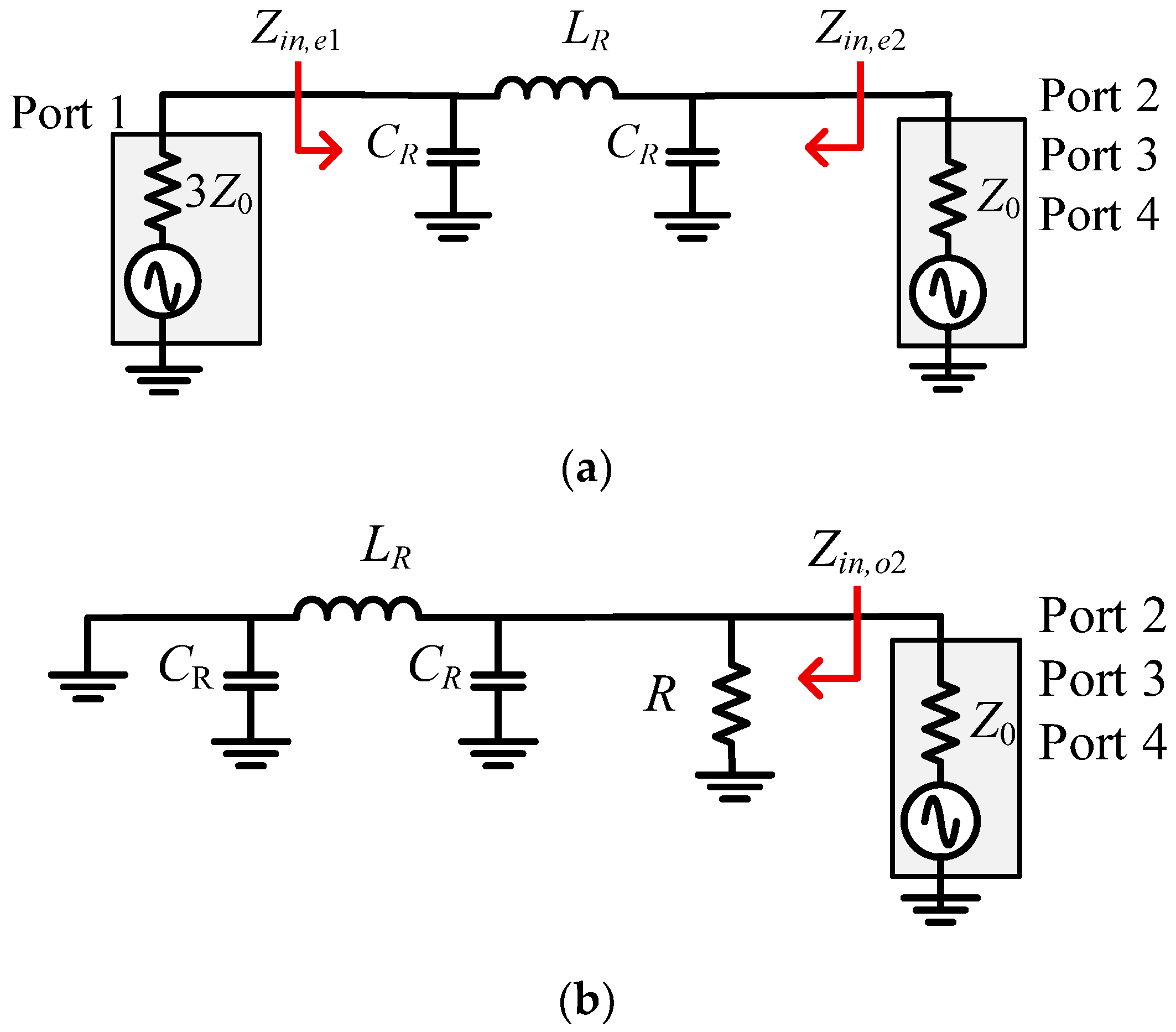
The WPD shown in Figure 6 exhibits a symmetric configuration, which allows the circuit to be divided into three identical parts for even- and odd-mode analysis [21,22]. In the even mode, the plane of symmetry is open when the signals at Ports 2, 3, and 4 have the same magnitude and phase. Therefore, no current flows through the common point containing the resistor , and the corresponding equivalent circuit is shown in Figure 7a. In the odd mode, Port 1 is short-circuited, while the common point between the output ports also becomes a short circuit. The corresponding equivalent circuit is shown in Figure 7b.
Figure 6.
Conventional one-Section 3-way Wilkinson power divider.
Figure 7.
Circuit analysis of the one-section power divider in (a) even mode and (b) odd mode. The input impedance looking into Port 1 and Port 2 for the even and odd modes are indicated by the red arrow.
In the even mode, the impedance and are calculated as follows.
In the odd-mode analysis, the value of can be found as follows.
All ports must be impedance-matched. In this case, the value of must be equal to 150 Ω, and equal to 50 Ω.
3.2. Two-Section Lumped Transmission Line Circuit WPD
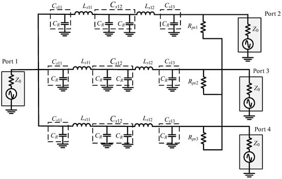
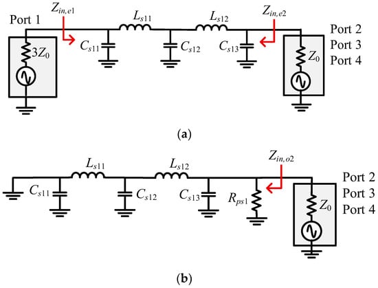
The proposed two-section lumped transmission line circuit WPD is shown in Figure 8. The even and odd mode analysis can be applied similarly to the one-section case. Equivalent circuits for even- and odd-mode analysis are shown in Figure 9.
Figure 8.
Lossless two-section lumped transmission line in a 3-way Wilkinson power divider.
Figure 9.
Circuit analysis of the two-section power divider in (a) even mode and (b) odd mode. The input impedances looking into Ports 1 and 2 for the even and odd modes are indicated by the red arrows.
The input impedance ( of the even mode can be calculated using (7)–(9).
where
and
Also, calculate by (10)–(12).
where
and
The input impedance () of odd mode can be calculated using (13)–(14).
where
Additionally, all port impedances in Figure 7 must be matched. The values of must be equal to 150 ohms, and equal to 50 ohms. Equations (4)–(14) can be used to calculate the lossless lumped transmission line circuit components. In the next section, loss and parasitic effects from the layout are considered.
4. Simulation and Measurement
The circuit in this work was designed for center frequency of 10 GHz. Simulations are performed using the one-section and two-section lumped transmission line in a Wilkinson power divider. The results of interest are the reflection coefficients, transmission coefficients, and isolation coefficients. Three types of results are compared: schematic simulation, layout simulation, and measurement.
4.1. Schematic Simulation
The lossless WPD using one- and two-section, shown in Figure 6 and Figure 8, was simulated for S-parameters, e.g., reflection coefficients, transmission coefficients, and isolation coefficients. The calculated component values are shown in Table 1.
Later, the results are compared with the layout simulation and measurement.
4.2. Layout Simulation
In this section, the layout parasitic extraction is investigated, considering only the TT process corner of the 0.12 um GaN technology. Only a two-section transmission line is used here; however, a one-section can be processed similarly. In this work, electromagnetic (EM) simulations of the layout were performed using the Momentum Microwave solver integrated within Keysight Advanced Design System [23]. The Momentum solver employs a 2.5D Method of Moments (MoM) approach based on multilayer dielectric Green’s functions [24]. The circuit layout was fabricated using the 0.12-μm RF GaN-on-SiC Process Design Kit (PDK) from WIN Semiconductors Corp. Bound/interconnection pads and passive device layouts were modeled using the dedicated foundry PDK components and interconnect layout rules. Open-boundary conditions (infinite horizontal substrate layers surrounded by open half-space) were applied. A non-adaptive planar mesh was used with a discretization density of 500 cells per wavelength at the highest simulation frequency. Mesh convergence was verified prior to final analysis. Increasing the mesh density beyond 500 cells per wavelength yielded a change of less than 0.01% in the calculated S-parameters (S11 and S21). Because a fixed (non-adaptive) meshing scheme is employed, the numerical results are fully deterministic and repeatable.
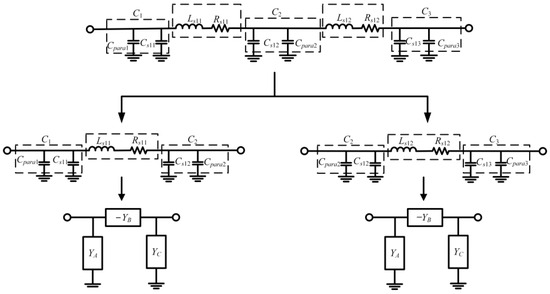
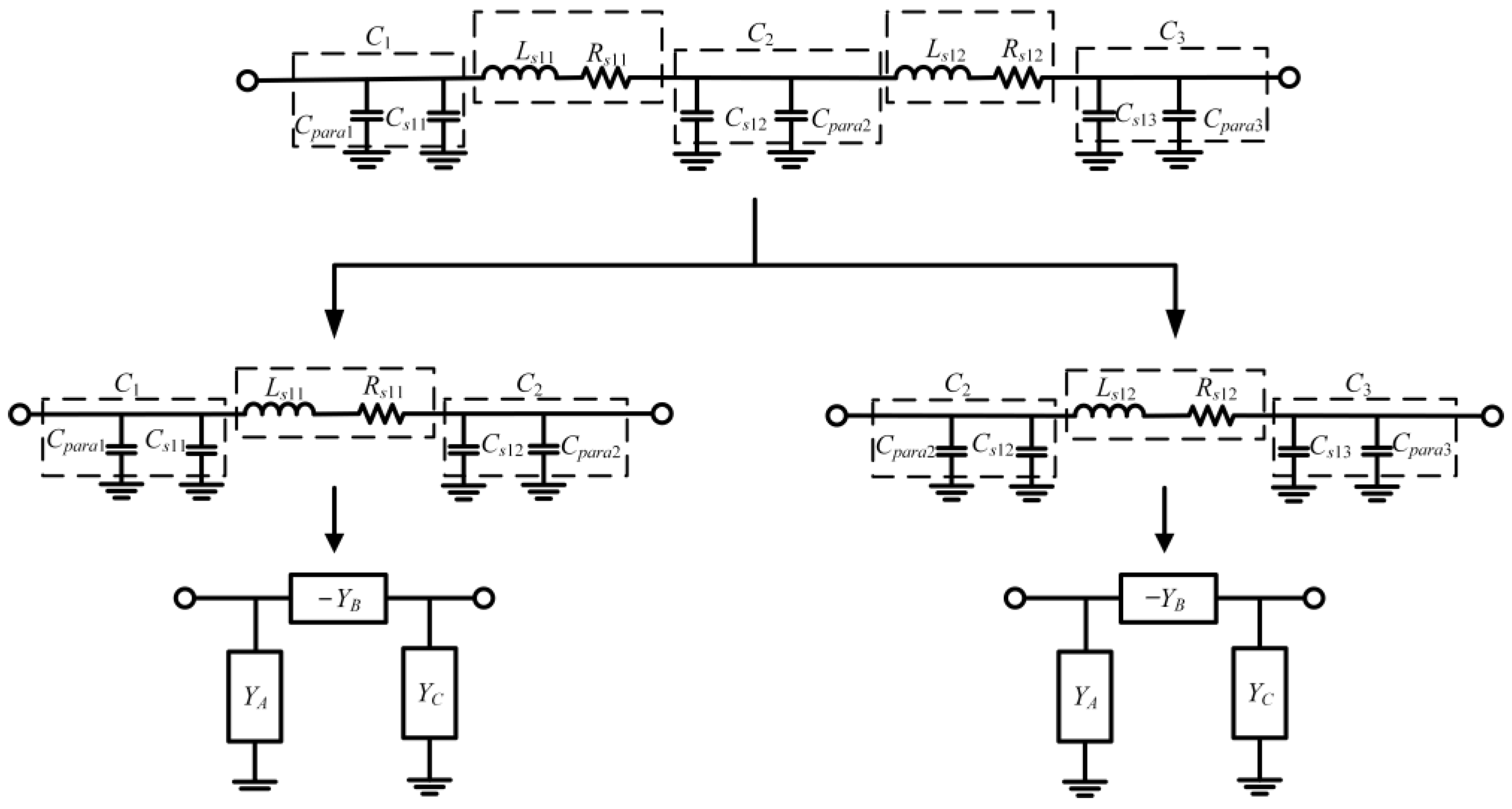
For the layout design, parasitic elements cause the circuit components to vary from the schematic ones. The parasitic capacitors vastly affect the layout performance, especially in X-band applications. To extract the parasitic capacitors from the layout, the two-section lumped transmission lines are divided into two circuits. The two circuits have the middle capacitors, , as the common elements. However, in the layout, the physical capacitors are present, along with parasitic capacitors from the layout. Figure 10 shows the parasitic capacitors and the divided circuits. Each single lumped transmission line simulation is studied using Y-parameters, as shown in the figure.
Figure 10.
Parasitic extraction using Y-parameter of a two-section transmission line. The arrows indicate the circuit division and Y-parameter extraction process.
The total capacitors, inductors, and resistors can be found from (15)–(17)
where and are the physical capacitances added to the parasitic capacitance, or are the inductors with losses modeled with resistors or .
The values of can be found from (7)–(14), allowing us to determine the parasitic capacitor value of the circuit by subtracting them from the total value. The total capacitance value is extracted from (15) and (17). The inductor (including parasitic inductance) and resistor values are found from (16).
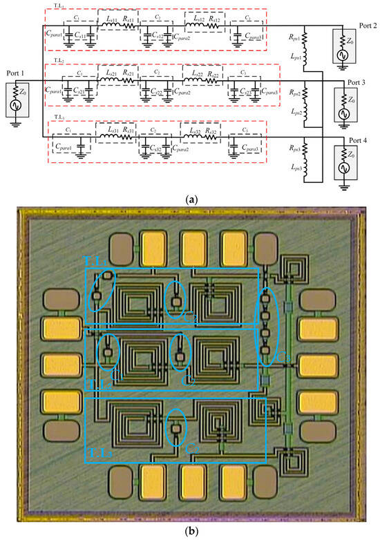
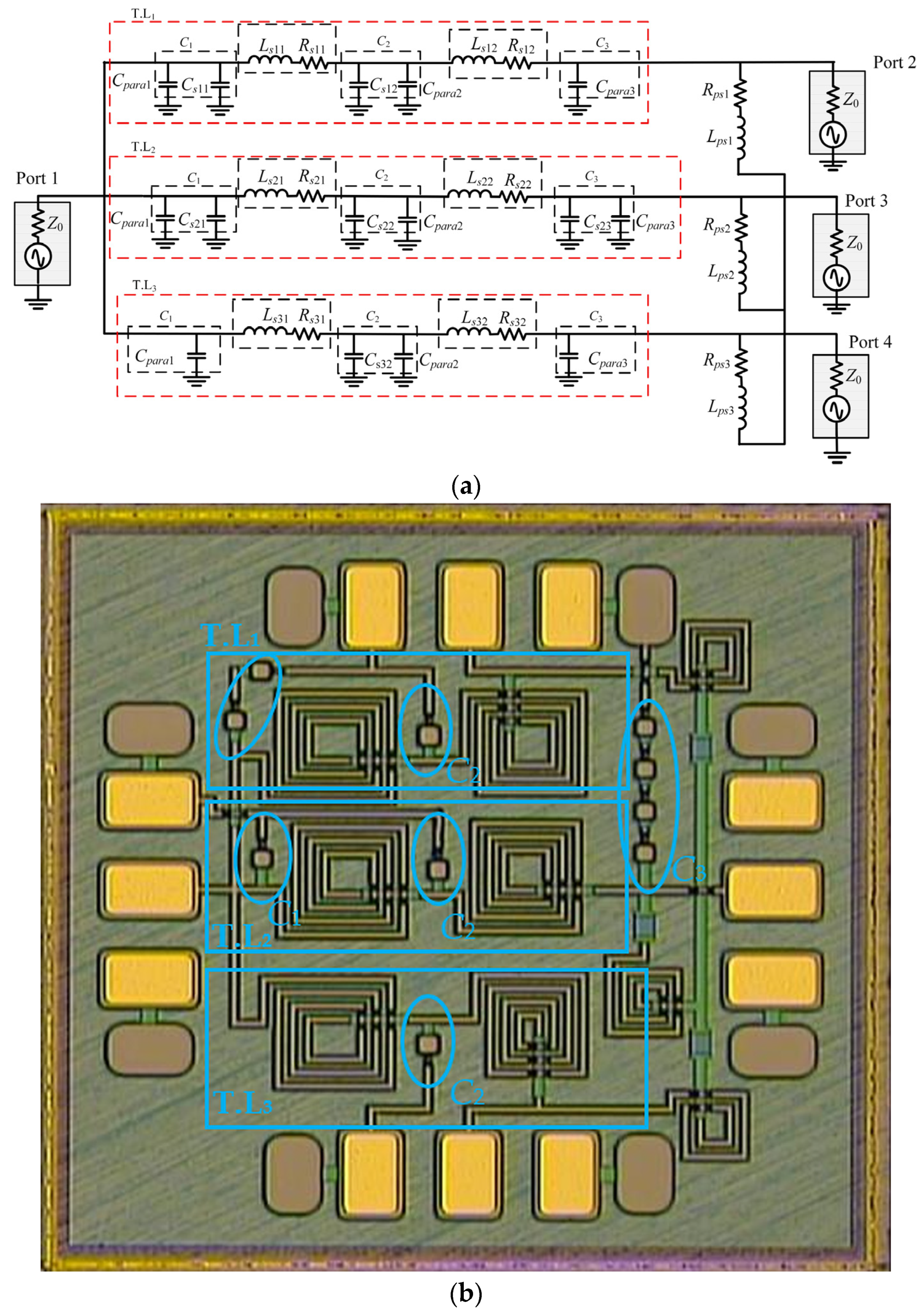
The proposed three-way power divider is illustrated in Figure 11, where Figure 11a depicts its equivalent circuit including parasitic capacitances, and Figure 11b shows its layout. The component values obtained from the schematic design cannot be directly applied to the layout because of the parasitic effects introduced by the physical implementation. Therefore, the component values need to be adjusted to account for these parasitic capacitances.
Figure 11.
Equivalent schematic of three-way power divider layout using two-section lumped transmission circuit. (a) Schematic and (b) layout.
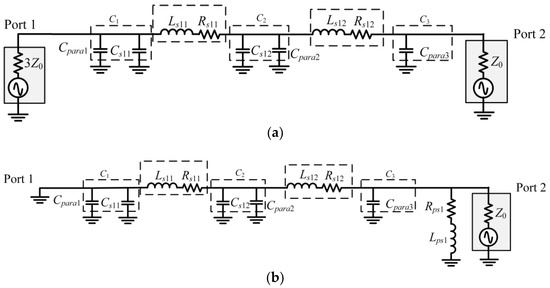
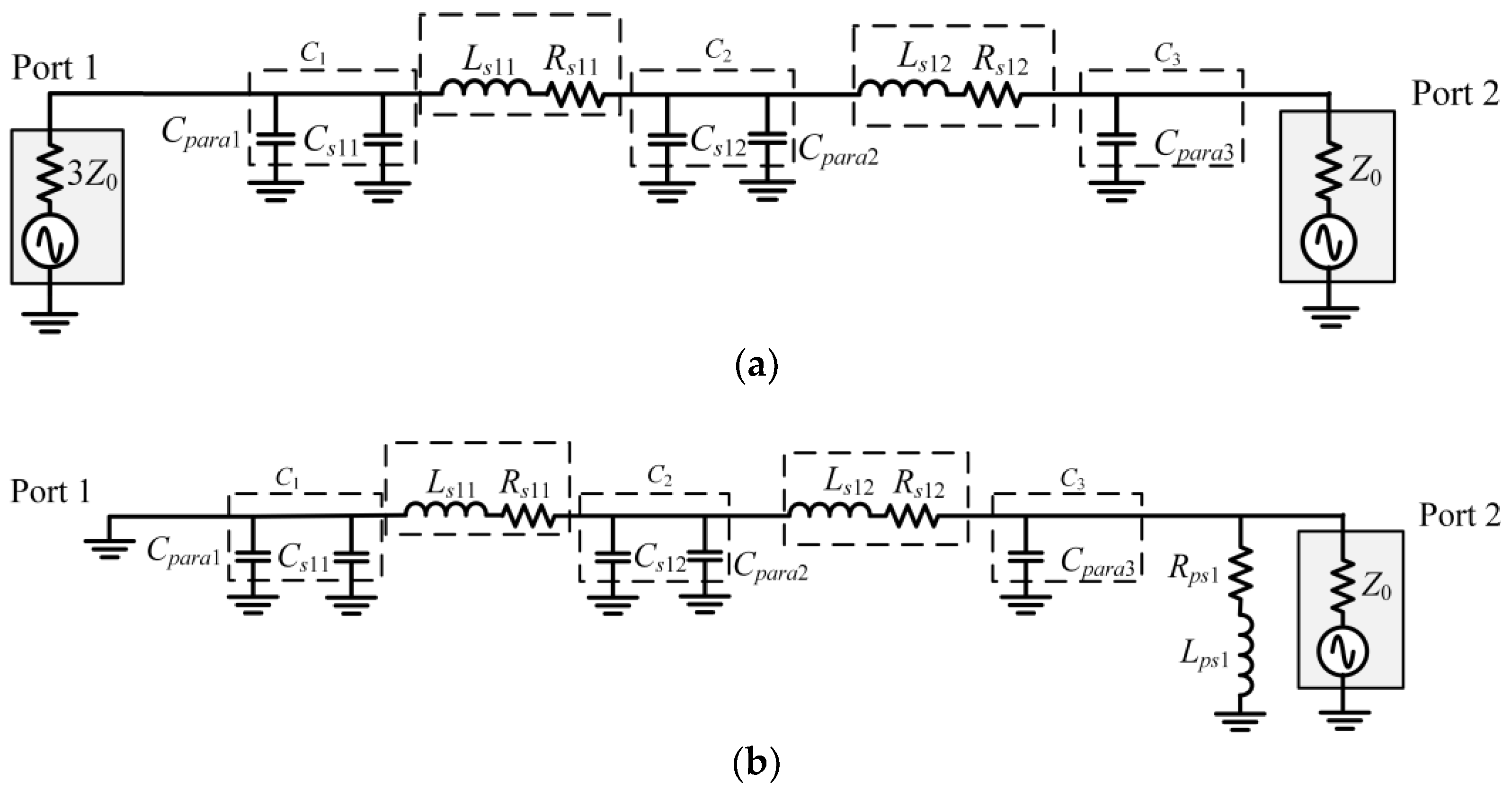
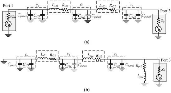
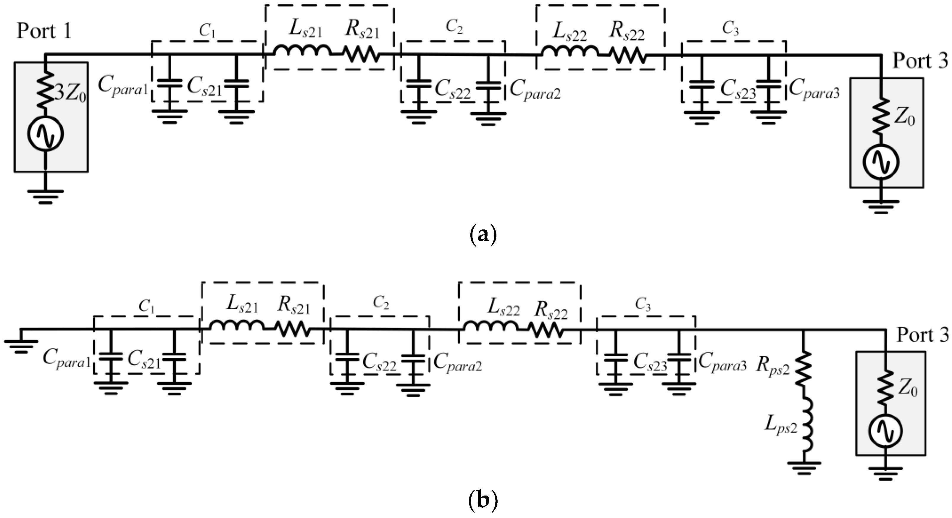
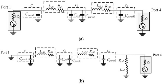
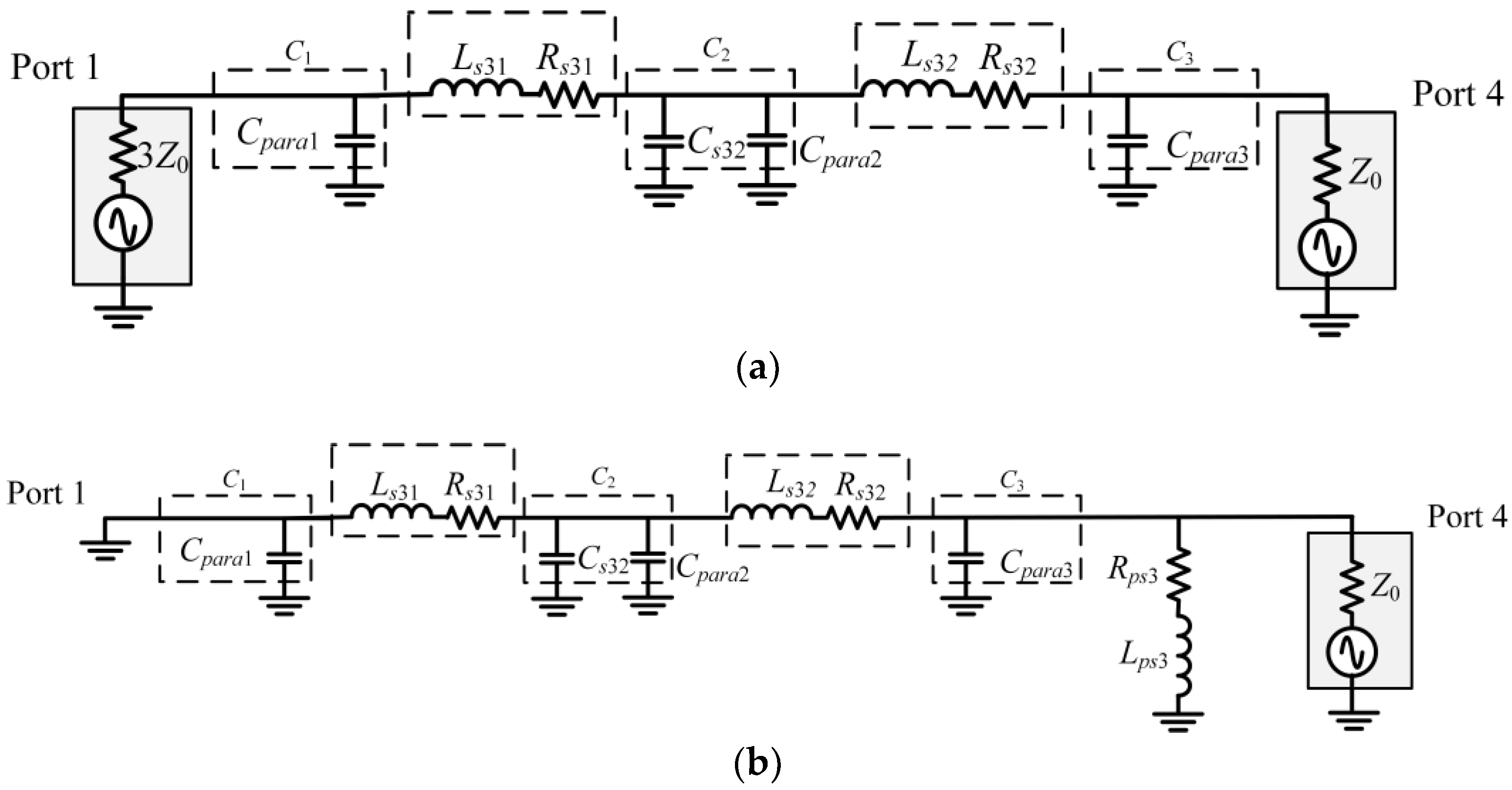
To optimize the component values, each transmission line section was treated individually. The equivalent circuits extracted from the layout for TL1, TL2, and TL3 are shown in Figure 12, Figure 13 and Figure 14, respectively. Each transmission line section was further represented by its corresponding even- and odd-mode equivalent circuits for impedance-matching analysis. In the layout design process, the inductors were first placed according to the floorplan, followed by the capacitors. The values of C1, C2, and C3 for each transmission line section were then optimized to achieve impedance matching for both the even- and odd-mode circuits at their respective ports. Since each transmission line layout has slightly different parasitic characteristics, the optimization was performed separately for each section.
Figure 12.
Analysis of port 1 and port 2 (TL1 in Figure 10) using (a) even mode and (b) odd mode.
Figure 13.
Analysis of port 1 and port 3 (TL2 in Figure 10) using (a) even mode and (b) odd mode.
Figure 14.
Analysis of port 1 and port 4 (TL3 in Figure 10) using (a) even mode and (b) odd mode.
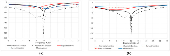
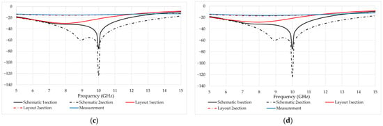
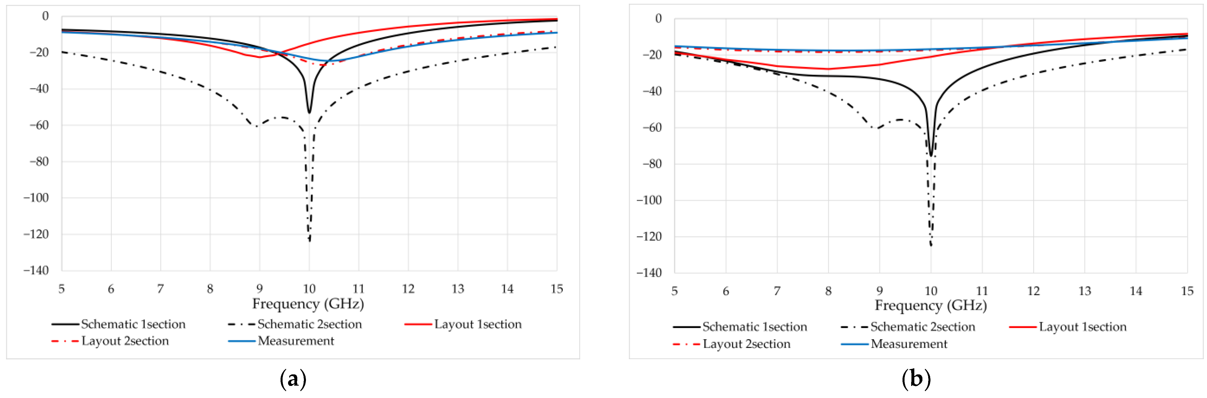
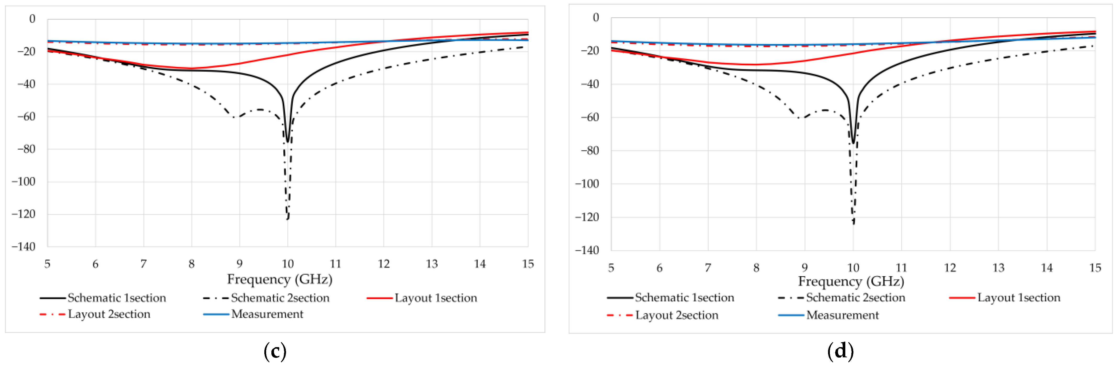
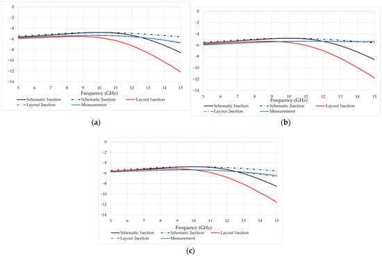
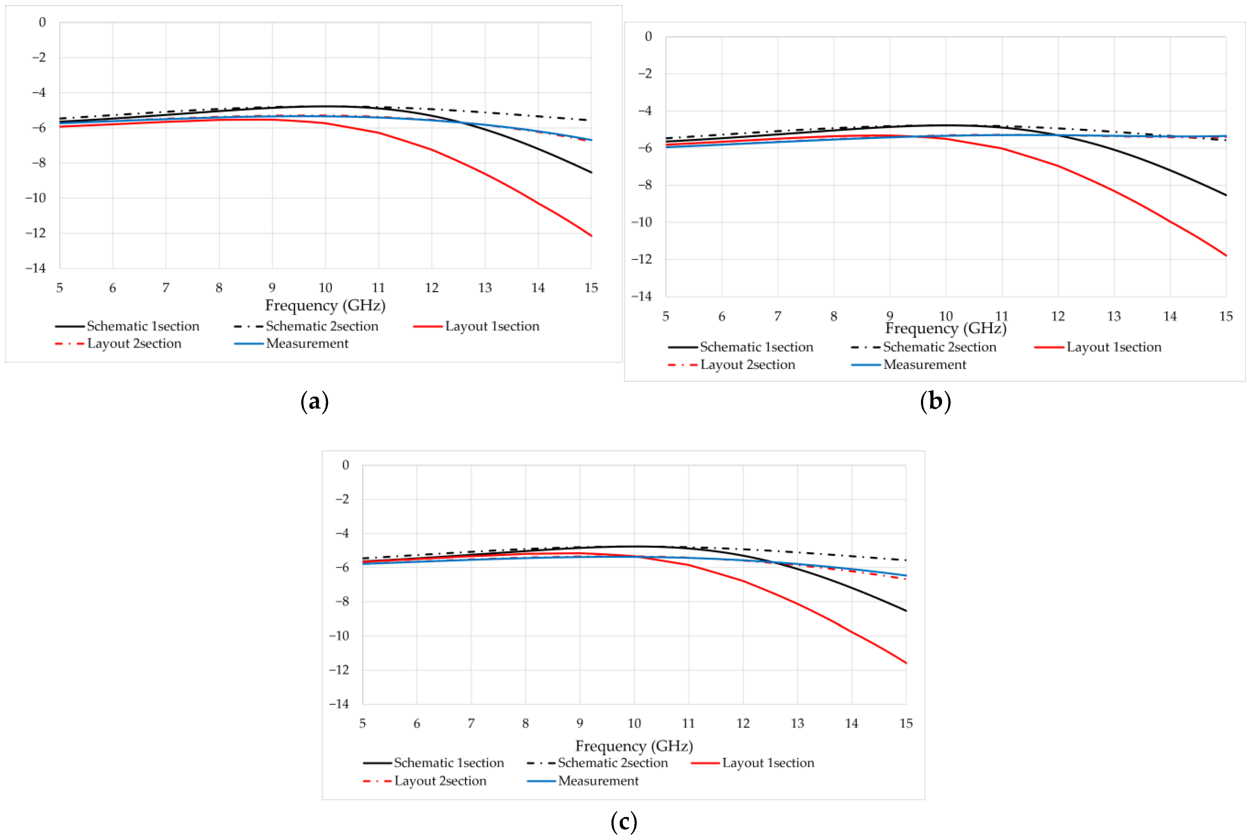
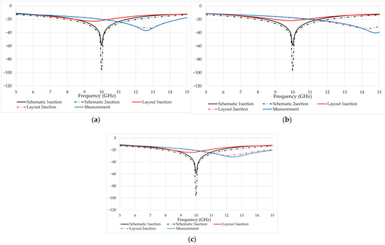
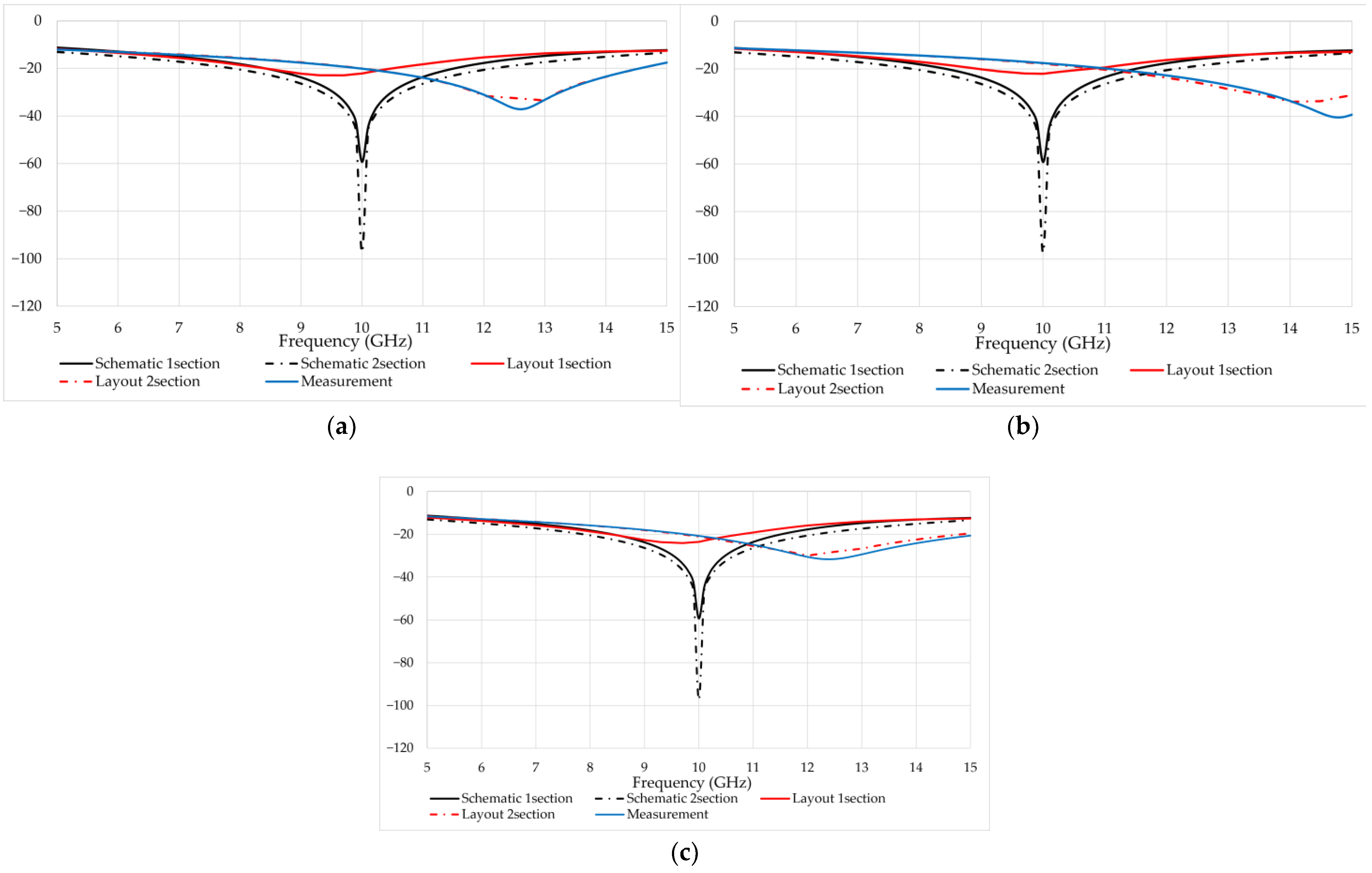
Table 2 shows the physical layout components after the layout optimization at 10 GHz. Note that some of the capacitors are physically omitted since the parasitic capacitance exceeds the required capacitance. Then, the layout circuits are simulated and measured for the reflection coefficients, transmission coefficients, and isolation coefficients, as shown in Figure 15, Figure 16 and Figure 17. In these figures, the schematic traces represent the ideal lumped-component simulation, the layout traces correspond to the layout EM simulation, and the measurement data represent the measured results. Clearly, the two-section lumped transmission lines WPD yield better reflection coefficients than those of the one-section. Therefore, only the two-section lumped transmission line WPD is used in comparison with the layout and measurement results. The reflection coefficients (S11, S22, S33, and S44) exhibit good agreement among all three results. The maximum reflection coefficient is −10 dB in both the ideal lumped-component simulation and the layout EM simulation, while the measured result is −10.09 dB, indicating an excellent matching performance with only 0.09 dB deviation from the simulated value.
Table 2.
Lumped model of TL schematic and layout at 10 GHz.
Figure 15.
Compare layout simulation of one-section, two-section, and measurement of circuit reflection coefficients for parameters (a) S11, (b) S22, (c) S33, (d) S44.
Figure 16.
Compare layout simulation of one-section, two-section, and measurement of circuit transmission coefficients for parameters (a) S12, (b) S13, (c) S14.
Figure 17.
Compare layout simulation of one-section, two-section, and measurement of circuit isolation coefficients for parameters (a) S23, (b) S24, (c) S34.
For the transmission coefficients (S12, S13, and S14), the minimum values are −5.677 dB (ideal lumped-component simulation), −7.632 dB (layout EM simulation), and −6.33 dB (measurement). Compared with the ideal simulation, the measured transmission shows an additional insertion loss of approximately 0.65 dB, whereas it differs from the EM/layout simulation by about 1.30 dB. This indicates that the measured performance lies between the ideal circuit simulation and the EM/layout prediction.
The isolation coefficients (S23, S24, and S34) are −13.9 dB (ideal lumped-component simulation), −15.7 dB (layout EM simulation), and −12.4 dB (measurement). The measured isolation is 1.5 dB higher (worse) than the schematic simulation and 3.3 dB higher than the EM/layout simulation. These discrepancies are mainly attributed to fabrication tolerances, conductor and dielectric losses, connector transitions, and measurement uncertainties, which are not fully captured in the simulations.
Overall, the measured results closely follow the simulated trends, confirming the validity of the proposed design. Although slight degradation in transmission and isolation is observed in the fabricated prototype, the agreement between simulation and measurement demonstrates that the design achieves the intended broadband performance.
For the measured results, a 4-port network analyzer (Keysight N5245B, 10 MHz–50 GHz) was used, with four-port RF GSG probes for contacting the measurement pads. SOLT calibration was performed using three calibration dies. The operating bandwidth of the proposed 3-way power divider is defined based on a −10 dB return loss criterion (|S11| ≤ −10 dB). As shown in Figure 15, the measured return loss satisfies|S11| ≤ −10 dB from GHz to GHz, centered at GHz. This corresponds to a fractional bandwidth (FBW) of 80.39%, calculated via:
Across this entire operational frequency band , the worst-case in-band performance parameters are evaluated as follows: Return Loss (S11): |S11|≤ −10 dB across Insertion Loss (S21): The maximum measured insertion loss within the band is 6.3244 dB (including the theoretical 3-way split loss of 4.77 dB); Isolation (S23): The isolation between output ports remains better than 12.401 dB over the entire window.
Although the measured performance aligns well with the overall predicted trend, slight discrepancies are observed in the insertion loss and input matching (). These deviations are primarily attributed to three physical mechanisms. (1) Substrate and ground loss: The finite conductivity of the GaN-on-SiC substrate, along with parasitic inductance/resistance from ground vias, adds unmodeled ohmic loss in the signal path. (2) Unmodeled interconnect parasitics: Micro-scale layout discontinuities, T-junction step capacitances, and via-hole grounding inductances introduce stray parasitics that cause a slight frequency shift and degradation in impedance matching (). (3) Measurement setup and probing tolerances: Imperfections in SOLT calibration and probe-to-pad contact resistance during on-wafer GSG probing introduce minor measurement uncertainties that affect both loss and return loss limits.
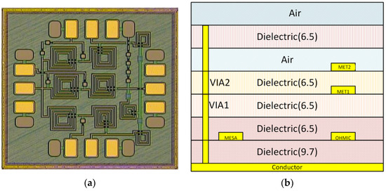
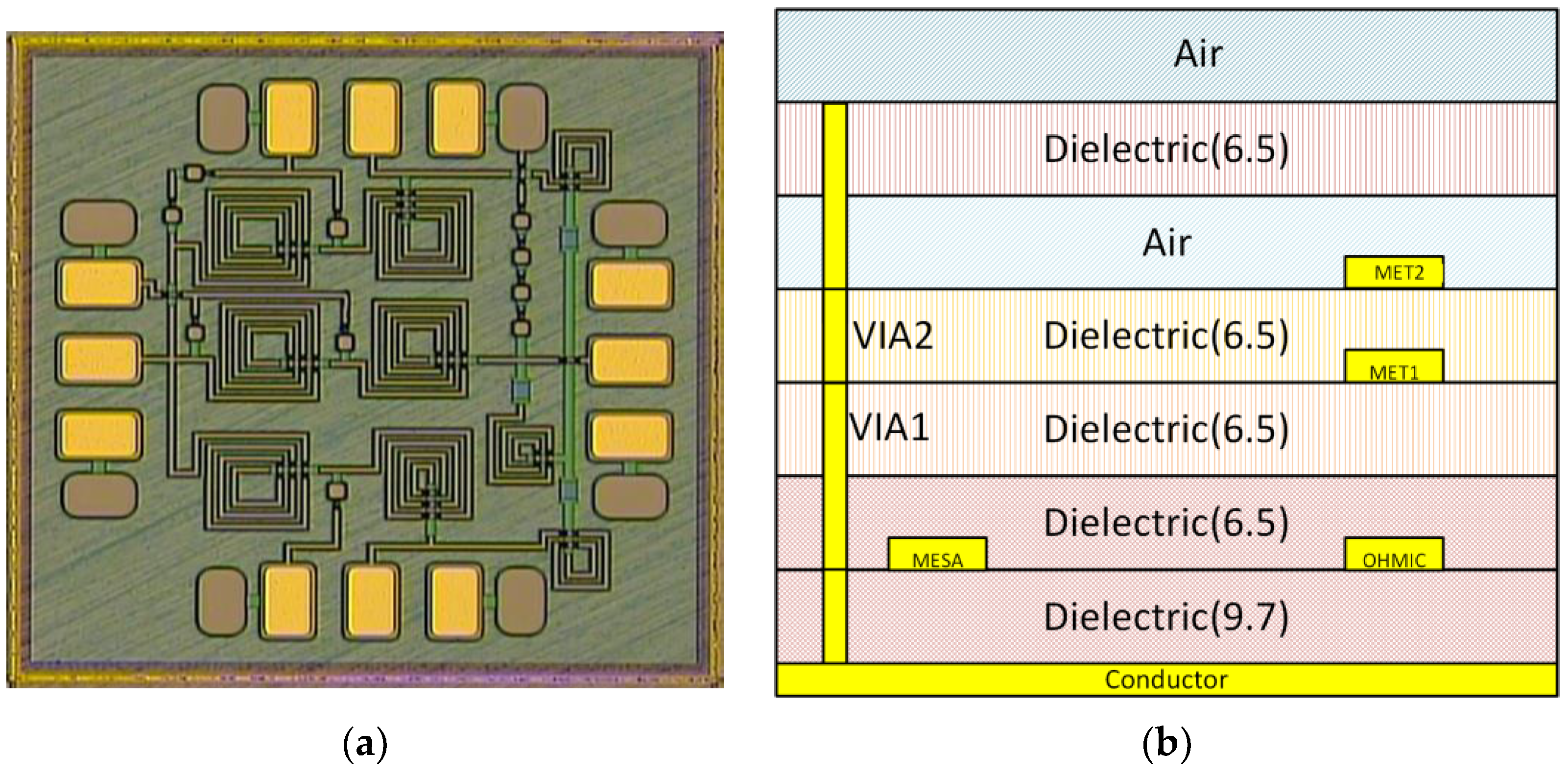
The chip photograph is shown in Figure 18. Table 3 presents a comparison between the three-way and four-way power dividers. The fractional bandwidth (FBW) is calculated using Equation (11). Because different return-loss criteria are adopted in the reported designs, including −10 dB for [25,26,27,28], −12 dB for [29], −12.3 dB for [10], and −13 dB for [30], a −13 dB return-loss criterion is adopted to evaluate the fractional bandwidth (FBW) of the proposed power divider for comparison with the referenced designs.
Figure 18.
(a) Die micrograph and (b) schematic cross-sectional view of the metal-layer structure of the proposed lumped-element Wilkinson power divider fabricated using a GaN MMIC process.
Table 3.
Comparison Table of Three- and Four-Way Power Dividers.
As shown in Table 3, under the specified return-loss criterion, the proposed power divider provides a wide fractional bandwidth while maintaining a compact chip size. The comparison is intended to highlight the bandwidth and chip-area characteristics of the proposed design relative to the selected reported works.
5. Conclusions
The design and analysis of a three-way wideband Wilkinson power divider are presented using a two-section cascaded lumped transmission line circuit. By using a smaller electrical-length section, the lumped transmission line circuits expand their characteristic impedance and electrical-length behavior over a wider bandwidth than the conventional single-section lumped transmission line circuit. In the design for X-band applications, parasitic capacitors play an important role in layout design. A parasitic extraction method is presented in this work for capacitor value selection. The layout is designed to have a compact size at (0.03λo × 0.03λo). The −10 dB fractional bandwidth is 80.39%. The amplitude balance is 0.1 dB. The phase balance is 5.8° (−13 dB fractional bandwidth of 52.4%, while the amplitude and phase balance are 0.04 dB and 4.9°). Overall, the circuit is compact and has good performance for X-band applications.
Author Contributions
Conceptualization, C.P. and S.W.; Methodology, C.P. and P.W.; Software, P.W.; Validation, P.W., C.P. and S.W.; Writing—original draft preparation, P.W.; Writing—review and editing, C.P. and S.W.; Supervision, C.P. and S.W. All authors have read and agreed to the published version of the manuscript.
Funding
This work was financially supported by King Mongkut’s Institute of Technology Ladkrabang [KREF016613]. This work is also supported by the National Taipei University of Technology-King Mongkut’s Institute of Technology Ladkrabang Joint Research Program (NTUT-KMITL No. NTUT-KMITL-113-02) and the National Science and Technology Council under NSTC 113-2218-E-A49-020-.
Data Availability Statement
The data supporting the findings of this study are available within the article, but underlying raw data are restricted due to confidentiality agreements.
Acknowledgments
The authors would like to express their sincere gratitude to Lab 410 at National Taipei University of Technology (NTUT) for providing technical support and assistance.
Conflicts of Interest
The authors declare no conflicts of interest.
References
- Wang, L.; Li, J.; Wang, X.; Zhong, Y.; Tong, J.; Cao, W.; Zhong, Q. An On-Chip Planar Broadband 3-Way Power Divider for Josephson Voltage Circuits. IEEE Trans. Appl. Supercond. 2021, 31, 1500104. [Google Scholar] [CrossRef] [Scilit]
- Cheng, S.; Pavlick, M. Synthesis of an N-Way Arbitrary Power Divider. In Proceedings of the 2017 47th European Microwave Conference, (EuMC), Nuremberg, Germany, 10–12 October 2017; pp. 392–395. [Google Scholar]
- Jin, Z.-F.; Xu, J.; Zhao, M.; Wan, H.; Liu, F.; Hou, Z. A Compact Wideband Lumped-Element Wilkinson Power Divider Using Inverting Coupled Coil. IEEE Microw. Wirel. Technol. Lett. 2024, 34, 599–602. [Google Scholar] [CrossRef] [Scilit]
- Pakasiri, C.; Kongchayasukwat, T. Improvement of Transmission Line Circuit on Lossy Substrate with Application on Phase Shifter Design. In Proceedings of the 2019 7th International Electrical Engineering Congress (iEECON), Hua Hin, Thailand, 6–8 March 2019; pp. 1–4. [Google Scholar]
- Kawai, T.; Mizuno, H.; Ohta, I.; Enokihara, A. Lumped-Element Quadrature Wilkinson Power Divider. In Proceedings of the 2009 Asia Pacific Microwave Conference (APMC 2009), Singapore, 7–10 December 2009; pp. 1012–1015. [Google Scholar]
- Phinney, J.W.; Perreault, D.J.; Lang, J.H. Synthesis of Lumped Transmission-Line Analogs. IEEE Trans. Power Electron. 2007, 22, 1531–1542. [Google Scholar] [CrossRef] [Scilit]
- Wang, F.; Zhang, X.; Wang, X. A Novel Multi-Section Lumped Element Topology for Wilkinson Power Divider Design. In Proceedings of the 16th UK-Europe-China Workshop on Millimetre Waves and Terahertz Technologies (UCMMT), Guangzhou, China, 31 August–3 September 2023; pp. 1–3. [Google Scholar]
- Wang, X.; Ma, Z.; Ohira, M. Theory and Experiment of Two-Section Two-Resistor Wilkinson Power Divider with Two Arbitrary Frequency Bands. IEEE Trans. Microw. Theory Tech. 2018, 66, 1291–1300. [Google Scholar] [CrossRef] [Scilit]
- Xiao, Y.; Ning, J.; Cheng, J.; Xia, B. A Compact 1-to-4 Broadband Planar Multi-Section Wilkinson Power Divider. In Proceedings of the 2022 IEEE MTT-S International Wireless Symposium (IWS), Harbin, China, 12–15 August 2022; pp. 1–3. [Google Scholar]
- Ding, Y.; Wan, J.; Yan, Y.; Liang, X. A Novel Compact, Wideband Four-Way Wilkinson Power Divider with an Improved Isolation Topology. IEEE Microw. Wirel. Technol. Lett. 2023, 33, 1119–1122. [Google Scholar] [CrossRef] [Scilit]
- Fu, J.; Wang, Z.; Lv, B.; Yang, Z.; Wu, Q. A New Compact Three-Way Wilkinson Power Divider Based on LTCC Technology. In Proceedings of the 2015 Asia-Pacific Microwave Conference (APMC), Nanjing, China, 6–9 December 2015; pp. 1–4. [Google Scholar]
- Elsbury, M.M.; Dresselhaus, P.D.; Bergren, N.F.; Burroughs, C.J.; Benz, S.P.; Popovic, Z. Broadband Lumped-Element Integrated N-Way Power Dividers for Voltage Standards. IEEE Trans. Microw. Theory Tech. 2009, 57, 2055–2063. [Google Scholar] [CrossRef]
- Doan, N.T.T.; Ngo, T.B.; Yoon, S.W. Compact wideband CMOS lumped-element Wilkinson power divider with asymmetric negative capacitance circuit. Electron. Lett. 2020, 56, 1065–1067. [Google Scholar] [CrossRef] [Scilit]
- Yoon, T.W.; Kim, D.S.; Yook, J.M. Compact and low-loss Wilkinson power divider using a high-Q spiral inductor on a sapphire substrate. Microw. Opt. Technol. Lett. 2018, 60, 1703–1707. [Google Scholar] [CrossRef] [Scilit]
- Cheng, J.-D.; Xia, B.; Xiong, C.; Wu, L.-S.; Mao, J.-F. An Unequal Wilkinson Power Divider Based on Integrated Passive Device Technology and Parametric Model. IEEE Microw. Wirel. Compon. Lett. 2022, 32, 281–284. [Google Scholar] [CrossRef] [Scilit]
- Xie, B.; Wang, C.; Kumar, A.; Wu, Q.; Zhao, M. Ultra-compact wideband dual-mode Wilkinson power divider based on thin film integrated passive device fabrication technology. J. Electromagn. Waves Appl. 2020, 35, 163–175. [Google Scholar] [CrossRef] [Scilit]
- Ju, I.; Cho, M.-K.; Song, I.; Cressler, J.D. A Compact, Wideband Lumped-Element Wilkinson Power Divider/Combiner Using Symmetric Inductors with Embedded Capacitors. IEEE Microw. Wirel. Compon. Lett. 2016, 26, 595–597. [Google Scholar] [CrossRef] [Scilit]
- Barakat, A.; Pokharel, R.K. High Quality Factor Miniaturized CMOS Transmission Lines Using Cascaded T-Networks for 60 GHz Millimeter Wave Applications. Electronics 2024, 13, 3748. [Google Scholar] [CrossRef] [Scilit]
- Lopez-Villegas, J.M.; Samitier, J.; Cane, C.; Losantos, P.; Bausells, J. Improvement of the quality factor of RF integrated inductors by layout optimization. IEEE Trans. Microw. Theory Tech. 2000, 48, 76–83. [Google Scholar] [CrossRef] [Scilit]
- Büyüktas, K.; Koller, K.; Müller, K.-H.; Geiselbrechtinger, A. A New Process for On-Chip Inductors with High Q-Factor Performance. Int. J. Microw. Sci. Technol. 2010, 2010, 517187. [Google Scholar] [CrossRef] [Scilit]
- Wilkinson, E.J. An N-Way Hybrid Power Divider. IRE Trans. Microw. Theory Tech. 1960, 8, 116–118. [Google Scholar] [CrossRef] [Scilit]
- Dib, N.; Khodier, M. Design and optimization of multi-band Wilkinson power divider. Int. J. RF Microw. Comput.-Aided Eng. 2008, 18, 14–20. [Google Scholar] [CrossRef] [Scilit]
- Keysight Technologies, Advanced Design System (ADS), version 2014; Keysight Technologies: Santa Rosa, CA, USA, 2014.
- Keysight Technologies. Momentum Theory of Operation, PathWave Design Engineering Documentation, 2010. Available online: https://docs.keysight.com/display/genesys2010/Momentum+Theory+of+Operation (accessed on 4 September 2026).
- Wang, F.; Wang, H. An N-Way Transformer Based Wilkinson Power Divider in CMOS. In Proceedings of the 2016 IEEE MTT-S International Microwave Symposium (IMS), San Francisco, CA, USA, 22–27 May 2016. [Google Scholar]
- Lai, Y.-A.; Lin, C.-M.; Chiu, J.-C.; Lin, C.-H.; Wang, Y.-H. A Compact Ka-Band Planar Three-Way Power Divider. IEEE Microw. Wirel. Compon. Lett. 2007, 17, 840–842. [Google Scholar] [CrossRef] [Scilit]
- Tsitsos, S.P.; Giannenas, I.C. Compact Three-Way Planar Power Divider with a Simple Structure. Int. J. Microw. Wirel. Technol. 2024, 16, 69–74. [Google Scholar] [CrossRef] [Scilit]
- Franzese, A.; Negra, R.; Malignaggi, A. An N-Way Single-Inductor High-Pass Power Divider for 5G Applications. IEEE Solid-State Circuits Lett. 2022, 5, 5–8. [Google Scholar] [CrossRef] [Scilit]
- Zhang, Q.; Ye, Z.; Li, G.; Wang, X. Comparisons of Two Types 4-Way Power Divider Based on the T-Coil Model. In Proceedings of the 2025 International Conference on Microwave and Millimeter Wave Technology (ICMMT), Xi’an, China, 19–22 May 2025; pp. 1–3. [Google Scholar]
- Hsiao, C.-Y.; Wu, C.-T.M.; Kuo, C.-N. A W-Band 1-dB Insertion Loss Wilkinson Power Divider Using Silicon-Based Integrated Passive Device. IEEE Microw. Wirel. Compon. Lett. 2021, 31, 654–657. [Google Scholar] [CrossRef] [Scilit]



Disclaimer/Publisher’s Note: The statements, opinions and data contained in all publications are solely those of the individual author(s) and contributor(s) and not of MDPI and/or the editor(s). MDPI and/or the editor(s) disclaim responsibility for any injury to people or property resulting from any ideas, methods, instructions or products referred to in the content. |
© 2026 by the authors. Licensee MDPI, Basel, Switzerland. This article is an open access article distributed under the terms and conditions of the Creative Commons Attribution (CC BY) license.